US7030436B2 - Embedded DRAM gain memory cell having MOS transistor body provided with a bi-polar transistor charge injecting means - Google Patents
Embedded DRAM gain memory cell having MOS transistor body provided with a bi-polar transistor charge injecting means Download PDFInfo
- Publication number
- US7030436B2 US7030436B2 US10/309,873 US30987302A US7030436B2 US 7030436 B2 US7030436 B2 US 7030436B2 US 30987302 A US30987302 A US 30987302A US 7030436 B2 US7030436 B2 US 7030436B2
- Authority
- US
- United States
- Prior art keywords
- horizontal
- region
- transistor
- mos transistor
- floating body
- Prior art date
- Legal status (The legal status is an assumption and is not a legal conclusion. Google has not performed a legal analysis and makes no representation as to the accuracy of the status listed.)
- Expired - Fee Related, expires
Links
- 230000015654 memory Effects 0.000 title claims abstract description 107
- 238000007667 floating Methods 0.000 claims abstract description 80
- 210000000746 body region Anatomy 0.000 claims abstract description 39
- 238000000034 method Methods 0.000 claims description 35
- 239000000758 substrate Substances 0.000 claims description 26
- 238000012545 processing Methods 0.000 claims description 5
- 230000008859 change Effects 0.000 claims description 4
- 230000008878 coupling Effects 0.000 claims description 4
- 238000010168 coupling process Methods 0.000 claims description 4
- 238000005859 coupling reaction Methods 0.000 claims description 4
- 230000002441 reversible effect Effects 0.000 claims description 2
- 239000003990 capacitor Substances 0.000 description 25
- 238000005516 engineering process Methods 0.000 description 13
- 239000004065 semiconductor Substances 0.000 description 9
- 238000004519 manufacturing process Methods 0.000 description 5
- 230000008569 process Effects 0.000 description 5
- 238000012546 transfer Methods 0.000 description 5
- 230000003321 amplification Effects 0.000 description 4
- 230000008901 benefit Effects 0.000 description 4
- 238000010586 diagram Methods 0.000 description 4
- 238000003199 nucleic acid amplification method Methods 0.000 description 4
- 230000000295 complement effect Effects 0.000 description 3
- 238000002955 isolation Methods 0.000 description 3
- 230000009467 reduction Effects 0.000 description 3
- 238000013459 approach Methods 0.000 description 2
- 230000015556 catabolic process Effects 0.000 description 2
- 238000004891 communication Methods 0.000 description 2
- 238000013461 design Methods 0.000 description 2
- 230000005669 field effect Effects 0.000 description 2
- 239000012212 insulator Substances 0.000 description 2
- 230000010354 integration Effects 0.000 description 2
- 230000000873 masking effect Effects 0.000 description 2
- 238000012986 modification Methods 0.000 description 2
- 230000004048 modification Effects 0.000 description 2
- 239000007787 solid Substances 0.000 description 2
- 230000003213 activating effect Effects 0.000 description 1
- 230000001010 compromised effect Effects 0.000 description 1
- 230000007423 decrease Effects 0.000 description 1
- 230000003247 decreasing effect Effects 0.000 description 1
- 238000006731 degradation reaction Methods 0.000 description 1
- 238000001514 detection method Methods 0.000 description 1
- 238000011161 development Methods 0.000 description 1
- 230000006870 function Effects 0.000 description 1
- 230000036039 immunity Effects 0.000 description 1
- 239000011810 insulating material Substances 0.000 description 1
- 230000000670 limiting effect Effects 0.000 description 1
- 239000000463 material Substances 0.000 description 1
- 238000004806 packaging method and process Methods 0.000 description 1
- 239000002245 particle Substances 0.000 description 1
- 230000002093 peripheral effect Effects 0.000 description 1
- 238000004886 process control Methods 0.000 description 1
- 238000012827 research and development Methods 0.000 description 1
- 229910052710 silicon Inorganic materials 0.000 description 1
- 239000010703 silicon Substances 0.000 description 1
- 230000003068 static effect Effects 0.000 description 1
Images


Classifications
-
- H—ELECTRICITY
- H10—SEMICONDUCTOR DEVICES; ELECTRIC SOLID-STATE DEVICES NOT OTHERWISE PROVIDED FOR
- H10B—ELECTRONIC MEMORY DEVICES
- H10B12/00—Dynamic random access memory [DRAM] devices
-
- H—ELECTRICITY
- H01—ELECTRIC ELEMENTS
- H01L—SEMICONDUCTOR DEVICES NOT COVERED BY CLASS H10
- H01L27/00—Devices consisting of a plurality of semiconductor or other solid-state components formed in or on a common substrate
- H01L27/02—Devices consisting of a plurality of semiconductor or other solid-state components formed in or on a common substrate including semiconductor components specially adapted for rectifying, oscillating, amplifying or switching and having at least one potential-jump barrier or surface barrier; including integrated passive circuit elements with at least one potential-jump barrier or surface barrier
- H01L27/04—Devices consisting of a plurality of semiconductor or other solid-state components formed in or on a common substrate including semiconductor components specially adapted for rectifying, oscillating, amplifying or switching and having at least one potential-jump barrier or surface barrier; including integrated passive circuit elements with at least one potential-jump barrier or surface barrier the substrate being a semiconductor body
- H01L27/06—Devices consisting of a plurality of semiconductor or other solid-state components formed in or on a common substrate including semiconductor components specially adapted for rectifying, oscillating, amplifying or switching and having at least one potential-jump barrier or surface barrier; including integrated passive circuit elements with at least one potential-jump barrier or surface barrier the substrate being a semiconductor body including a plurality of individual components in a non-repetitive configuration
- H01L27/07—Devices consisting of a plurality of semiconductor or other solid-state components formed in or on a common substrate including semiconductor components specially adapted for rectifying, oscillating, amplifying or switching and having at least one potential-jump barrier or surface barrier; including integrated passive circuit elements with at least one potential-jump barrier or surface barrier the substrate being a semiconductor body including a plurality of individual components in a non-repetitive configuration the components having an active region in common
- H01L27/0705—Devices consisting of a plurality of semiconductor or other solid-state components formed in or on a common substrate including semiconductor components specially adapted for rectifying, oscillating, amplifying or switching and having at least one potential-jump barrier or surface barrier; including integrated passive circuit elements with at least one potential-jump barrier or surface barrier the substrate being a semiconductor body including a plurality of individual components in a non-repetitive configuration the components having an active region in common comprising components of the field effect type
-
- H—ELECTRICITY
- H01—ELECTRIC ELEMENTS
- H01L—SEMICONDUCTOR DEVICES NOT COVERED BY CLASS H10
- H01L29/00—Semiconductor devices adapted for rectifying, amplifying, oscillating or switching, or capacitors or resistors with at least one potential-jump barrier or surface barrier, e.g. PN junction depletion layer or carrier concentration layer; Details of semiconductor bodies or of electrodes thereof ; Multistep manufacturing processes therefor
- H01L29/66—Types of semiconductor device ; Multistep manufacturing processes therefor
- H01L29/68—Types of semiconductor device ; Multistep manufacturing processes therefor controllable by only the electric current supplied, or only the electric potential applied, to an electrode which does not carry the current to be rectified, amplified or switched
- H01L29/76—Unipolar devices, e.g. field effect transistors
- H01L29/772—Field effect transistors
- H01L29/78—Field effect transistors with field effect produced by an insulated gate
- H01L29/7841—Field effect transistors with field effect produced by an insulated gate with floating body, e.g. programmable transistors
Definitions
- the present invention relates generally to integrated circuits, and in particular to an embedded DRAM gain memory cell.
- An essential semiconductor device is semiconductor memory, such as a random access memory (RAM) device.
- RAM random access memory
- a RAM device allows the user to execute both read and write operations on its memory cells.
- Typical examples of RAM devices include dynamic random access memory (DRAM) and static random access memory (SRAM).
- DRAM is a specific category of RAM containing an array of individual memory cells, where each cell includes a capacitor for holding a charge and a transistor for accessing the charge held in the capacitor.
- the transistor is often referred to as the access transistor or the transfer device of the DRAM cell.
- FIG. 1 illustrates a portion of a DRAM memory circuit containing two neighboring DRAM cells 100 .
- Each cell 100 contains a storage capacitor 140 and an access field effect transistor or transfer device 120 .
- one side of the storage capacitor 140 is connected to a reference voltage (illustrated as a ground potential for convenience purposes).
- the other side of the storage capacitor 140 is connected to the drain of the transfer device 120 .
- the gate of the transfer device 120 is connected to a signal known in the art as a word line 180 .
- the source of the transfer device 120 is connected to a signal known in the art as a bit line 160 (also known in the art as a digit line).
- each cell 100 contains one bit of data (i.e., a logic “0” or logic “1”).
- the DRAM 240 contains a memory array 242 , row and column decoders 244 , 248 and a sense amplifier circuit 246 .
- the memory array 242 consists of a plurality of memory cells 200 (constructed as illustrated in FIG. 1 ) whose word lines 280 and bit lines 260 are commonly arranged into rows and columns, respectively.
- the bit lines 260 of the memory array 242 are connected to the sense amplifier circuit 246 , while its word lines 280 are connected to the row decoder 244 .
- Address and control signals are input on address/control lines 261 into the DRAM 240 and connected to the column decoder 248 , sense amplifier circuit 246 and row decoder 244 and are used to gain read and write access, among other things, to the memory array 242 .
- the column decoder 248 is connected to the sense amplifier circuit 246 via control and column select signals on column select lines 262 .
- the sense amplifier circuit 246 receives input data destined for the memory array 242 and outputs data read from the memory array 242 over input/output (I/O) data lines 263 .
- Data is read from the cells of the memory array 242 by activating a word line 280 (via the row decoder 244 ), which couples all of the memory cells corresponding to that word line to respective bit lines 260 , which define the columns of the array.
- One or more bit lines 260 are also activated.
- the sense amplifier circuit 246 connected to a bit line column detects and amplifies the data bit transferred from the storage capacitor of the memory cell to its bit line 260 by measuring the potential difference between the activated bit line 260 and a reference line which may be an inactive bit line.
- a reference line which may be an inactive bit line.
- the memory cells of dynamic random access memories are comprised of two main components, a field-effect transistor (FET) and a capacitor which functions as a storage element.
- FET field-effect transistor
- VLSI very large scale integrated
- One approach to embedded memory technology is based on the one transistor DRAM cell structure that utilizes the trench process employed in IBM's and Toshiba's DRAMs. (See generally, W. P. Noble et al., “The evolution of IBM CMOS DRAM Technology,” IBM J. Research and Development, 39-1/2, 167-188 (1995)). With trench technology, logic performance is not compromised. Trench technology provides a planar surface topology that enhances interconnect reliability while providing a DRAM storage capacitor with a large and conventional storage capacitance. However, additional masking levels are required in the logic technology to fabricate the trench capacitors.
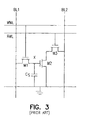
- FIG. 3 Another approach to embedded memory is based on a three transistor DRAM cell structure, shown in FIG. 3 .
- the three transistor DRAM cell structure was developed prior to the use of the trench capacitors or stacked capacitors now used in DRAMs. (See generally, J. Rabaey, Digital Integrated Circuits, Prentice Hall, 585-587 (1996)). A much smaller storage capacitor was utilized and compensated for by the gain of one of the transistors, in other words the first DRAMs developed used gain cells.
- These type of DRAM cells require only a minor modification of the conventional logic technology processes but occupy a large area due to the use of three transistors.
- the inventors have previously disclosed a DRAM gain cell using two transistors. (See generally, L. Forbes, “Merged Transistor Structure for Gain Memory Cell,” U.S. Pat. No. 5,732,014, issued 24 Mar. 1998, continuation granted as U.S. Pat. No. 5,897,351, issued 27 Apr. 1999). A number of other gain cells have also been disclosed. (See generally, Sunouchi et al., “A self-Amplifying (SEA) Cell for Future High Density DRAMs,” Ext. Abstracts of IEEE Int. Electron Device Meeting, pp. 465-468 (1991); M. Terauchi et al., “A Surrounding Gate Transistor (SGT) Gain Cell for Ultra High Density DRAMS,” VLSI Tech.
- SEA self-Amplifying
- FIG. 4 illustrates a portion of a DRAM memory circuit containing two neighboring gain cells, 401 and 403 .
- Each gain cell, 401 and 403 is separated from a substrate 405 by a buried oxide layer 407 .
- the gain cells, 401 and 403 are formed on the buried oxide 407 and thus have a floating body, 409 - 1 and 409 - 2 respectively, separating a source region 411 (shared for the two cells) and a drain region 413 - 1 and 413 - 2 .
- a bit/data line 415 is coupled to the drain regions 413 - 1 and 413 - 2 via bit contacts, 417 - 1 and 417 - 2 .
- a ground source 419 is coupled to the source region 411 .
- Wordlines or gates, 421 - 1 and 421 - 2 oppose the floating body regions 409 - 1 and 409 - 2 and are separated therefrom by a gate oxide, 423 - 1 and 423 - 2 .
- back gate bias is used to modulate the threshold voltage and consequently the conductivity of the NMOS transistor in each gain cell.
- the potential of the back gate body, 409 - 1 and 409 - 2 is made more positive by avalanche breakdown in the drain regions, 413 - 1 and 413 - 2 , and collection of the holes generated by the body, 409 - 1 and 409 - 2 .
- a more positive potential or forward bias applied to the body, 409 - 1 and 409 - 2 decreases the threshold voltage and makes the transistor more conductive when addressed. Charge storage is accomplished by this additional charge stored on the floating body, 409 - 1 and 409 - 2 .
- Reset is accomplished by forward biasing the drain-body n-p junction diode to remove charge from the body.
- a high density horizontally merged MOS-bipolar gain memory cell is realized for DRAM operation.
- the gain cell includes a horizontal MOS transistor having a source region, a drain region, and a floating body region therebetween.
- the gain cell includes a horizontal bi-polar transistor having an emitter region, a base region and a collector region.
- the collector region for the horizontal bi-polar transistor serves as the floating body region for the horizontal MOS transistor.
- a gate opposes the floating body region and is separated therefrom by a gate dielectric.
- the emitter region for the horizontal bi-polar transistor is coupled to a write data line.
- the gate is coupled to a read data word line.
- the source region is coupled to a read data bit line.
- FIG. 1 is a circuit diagram illustrating conventional dynamic random access memory (DRAM) cells.
- DRAM dynamic random access memory
- FIG. 2 is a block diagram illustrating a DRAM device.
- FIG. 3 is a schematic for an embedded memory based on a three transistor DRAM cell structure.
- FIG. 4 illustrates two neighboring one transistor gain cells as a portion of a memory array.
- FIG. 5A is a cross-sectional, perspective view illustrating an embodiment of a horizontally merged MOS-bipolar transistor gain memory cell according to the teachings of the present invention.
- FIG. 5B illustrates a top view of FIG. 5A in planar, CMOS technology with shallow trench oxide isolation.
- FIG. 5C illustrates an electrical equivalent circuit embodiment of the horizontally merged MOS-bipolar transistor gain memory cell indicating that the floating body well of the horizontal MOS transistor and the well to substrate capacitance acts as a storage capacitor.
- FIG. 6 is a block diagram illustrating an embodiment of an electronic system utilizing the embedded gain memory cells of the present invention.
- wafer and substrate are interchangeably used to refer generally to any structure on which integrated circuits are formed, and also to such structures during various stages of integrated circuit fabrication. Both terms include doped and undoped semiconductors, epitaxial layers of a semiconductor on a supporting semiconductor or insulating material, combinations of such layers, as well as other such structures that are known in the art.
- horizontal as used in this application is defined as a plane parallel to the conventional plane or surface of a wafer or substrate, regardless of the orientation of the wafer or substrate.
- vertical refers to a direction perpendicular to the horizontal as defined above. Prepositions, such as “on”, “side” (as in “sidewall”), “higher”, “lower”, “over” and “under” are defined with respect to the conventional plane or surface being on the top surface of the wafer or substrate, regardless of the orientation of the wafer or substrate.
- FIG. 5A is a cross-sectional, perspective view illustrating an embodiment of an embedded, horizontally merged MOS-bipolar transistor gain memory cell 501 according to the teachings of the present invention.
- the embedded, horizontally merged MOS-bipolar transistor gain memory cell 501 is formed in a p-type conductivity substrate 502 .
- An n-type conductivity well 505 is formed in the p-type conductivity substrate 502 .
- a more heavily doped p-type conductivity region (p+) 507 is formed in a portion of the p-type conductivity substrate 502 and in a portion of the n-type conductivity well 505 .
- the more heavily doped p-type conductivity region (p+) 507 serves as a source region 507 for a horizontal MOS transistor 509 portion of the horizontally merged MOS-bipolar transistor gain memory cell 501 .
- Another more heavily doped p-type conductivity region (p+) 511 is formed in another portion of the n-type conductivity well 505 .
- This more heavily doped p-type conductivity region (p+) 511 serves as the drain region 511 for the horizontal MOS transistor 509 portion of the horizontally merged MOS-bipolar transistor gain memory cell 501 .
- a gate 513 opposes the n-type conductivity well 505 between the source and the drain regions, 507 and 511 respectively.
- the n-type conductivity well 505 serves as a body region 505 and, more particularly, as a floating body region 505 for the horizontal MOS transistor 509 portion of the horizontally merged MOS-bipolar transistor gain memory cell 501 .
- the n-type conductivity well 505 can also be referred to as a floating body n-well 505 .
- the gate 513 is separated from the floating body region 505 by a gate dielectric 515 .
- a read data word line 517 is coupled to the gate 513 along rows of an array.
- any number of the horizontally merged MOS-bipolar transistor gain memory cell 501 shown in FIG. 5A can be arranged in an array on a semiconductor wafer.
- a read data bit line 519 is coupled to the drain region 511 along columns of such an array.
- a horizontal bi-polar transistor 521 completes the horizontally merged MOS-bipolar transistor gain memory cell 501 .
- the horizontal bi-polar transistor 521 includes an emitter region 523 , a base region 525 , and a collector region 527 .
- the emitter region 523 includes a heavily doped n-type conductivity region 523 (n+) formed in the p-type conductivity substrate 502 .
- the emitter region can also be referred to as an injector 523 .
- the base region 525 for the horizontal bi-polar transistor 521 portion of the is formed by the p-type conductivity substrate material.
- the base region 525 and the p-type conductivity substrate 502 are coupled to a ground potential.
- the collector region 527 for the horizontal bi-polar transistor 521 is formed from a portion of the floating body n-well 505 .
- the p+ drain region 511 is formed in the floating body n-well 505 and a portion of the floating body n-well 505 extends and/or wraps around the p+ drain region 511 to a side of the drain region 511 horizontally opposite from the side of the drain region 511 where the gate 513 is located.
- the floating body n-well 505 serves both as a floating body region 505 for the horizontal MOS transistor 509 and a portion of the floating body n-well also serves as the collector region 527 of the horizontal bi-polar transistor 521 .
- a write data bit line 529 is coupled to the emitter region 523 for the horizontal bi-polar transistor 521 portion of the horizontally merged MOS-bipolar transistor gain memory cell 501 .
- the write data bit line 529 can also be referred to as an emitter line 529 and/or an injector line 529 .
- the horizontal bi-polar transistor 521 is operable to inject a charge on to the floating body 505 of the horizontal MOS transistor 509 .
- the floating body 505 is operable to store charge by capacitive coupling to the gate 513 and a small stored charge from the same produces a change in the threshold voltage of the horizontal MOS transistor 509 .
- the horizontally merged MOS-bipolar transistor gain memory cell 501 can be formed or fabricated using planar CMOS processing techniques. As such, the present invention yields a horizontally merged MOS-bipolar transistor gain memory cell 501 which has an area equal to or less than 10 square photolithographic features (10F 2 ).
- FIG. 5B illustrates a top view of FIG. 5A in planar, CMOS technology with shallow trench oxide isolation 531 illustrated alongside the horizontally merged MOS-bipolar transistor gain memory cell 501 .
- the top view of FIG. 5A illustrates the heavily doped p-type conductivity source region 507 (p+).
- the gate 513 is shown above the floating body region 505 of the horizontal MOS transistor 509 portion of the horizontally merged MOS-bipolar transistor gain memory cell 501 .
- the portion of the floating body n-well 505 which serves as the collector region 527 for the horizontal bi-polar transistor 521 is seen from the top view on the opposite side of the drain region 511 from the gate's 513 location. From the top view embodiment of FIG. 5A , the p-type conductivity portion of the substrate which serves as the base region 525 for the horizontal bi-polar transistor 521 is viewable adjacent to the collector region 527 .
- the heavily doped n-type conductivity emitter region, or injector, 523 (n+) is viewable adjacent to the base region 525 .
- FIG. 5C illustrates an electrical equivalent circuit embodiment of the horizontally merged MOS-bipolar transistor gain memory cell 501 indicating that the floating body well 505 of the horizontal MOS transistor 509 and the floating body well 505 to substrate 502 capacitance acts as a storage capacitor 533 .
- the embodiment of FIG. 5C illustrates the horizontal MOS transistor 509 including the source region 507 , the gate 513 opposing the floating body region 505 , and the drain region 511 .
- a read data word line 517 is shown coupled to the gate 513 and a read data bit line 519 is coupled to the drain region 511 .
- FIG. 5C further illustrates the bi-polar transistor 521 including the collector region 527 , which is integrally formed with the floating body region 505 , the base region 525 , and the emitter, or injector, region 523 .
- the emitter region 523 is coupled to a write data bit line, emitter line, or injector line 529 .
- the base region 525 of the bi-polar transistor 521 which is integrally formed with the substrate 502 , is coupled to a ground potential.
- the floating body well 505 of the horizontal MOS transistor and the floating body well 505 to substrate 502 capacitance acts as a storage capacitor 533 .
- the sense device used to read the horizontally merged MOS-bipolar transistor gain memory cell 501 is the horizontal MOS transistor 509 which is addressed by the read data word line 517 .
- the horizontal MOS transistor 509 In the embodiment of a horizontal PMOS transistor 509 , if a negative charge or electrons are stored on the floating body 505 , then the n-type floating body 505 will be slightly forward biased and the horizontal MOS transistor 509 will be more conductive than normal.
- the horizontal bi-polar transistor 521 is an npn bi-polar transistor 521 .
- the horizontal bi-polar transistor 521 need not be a high performance device nor have a high current gain. Accordingly, the horizontal bi-polar transistor 521 can be a high yield structure.
- the read data word line 517 is driven positive to drive the floating n-type body 505 to a positive potential by capacitive coupling to the read data word line 517 .
- This positive potential serves to keep the floating body 505 reverse biased and avoid charge leakage.
- the horizontally merged MOS-bipolar transistor gain memory cell 501 can be erased by driving the drain 511 positive and the gate 513 negative to forward bias the drain-body p-n junction ( 511 - 505 junction).
- the drain-body p-n junction 511 - 505 junction.
- T. Ohsawa et al. “Memory Design Using One Transistor Gain Cell on SOI,” IEEE Int. Solid State Circuits Conv ., San Francisco, 152-153 (2002); S. Okhonin, M. Nagoga, J. M. Sallese, P. Fazan, “A SOI Capacitor-less IT-DRAM Cell,” Late News 2001 IEEE Intl. SOI Conference , Durango, Colo., 153-154).
- the horizontally merged MOS-bipolar transistor gain memory cell 501 can provide a very high gain and amplification of the stored charge on the floating body 505 of the horizontal, or lateral, PMOS sense transistor 509 .
- a small change in the threshold voltage caused by charge stored on the floating body 505 will result in a large difference in the number of holes conducted between the drain 511 and source of 507 the horizontal PMOS sense transistor 509 during the read data operation.
- the resulting horizontally merged MOS-bipolar transistor gain memory cell 501 has a very high density with a cell area of approximately 10F 2 , where F is the minimum feature size, and whose vertical extent is far less than the total height of a stacked capacitor or trench capacitor cell and access transistor.
- the cell can be fabricated without any modification of conventional CMOS logic technology.
- the sense transistor 509 would be an NMOS transistor with a p-type floating body.
- FIG. 6 is a block diagram of a processor-based system 600 utilizing embedded, horizontally merged MOS-bipolar transistor gain memory cells according to the various embodiments of the present invention. That is, the system 600 utilizes various embodiments of the horizontally merged MOS-bipolar transistor gain memory cell 501 illustrated in FIGS. 5A-5C .
- the processor-based system 600 may be a computer system, a process control system or any other system employing a processor and associated memory.
- the system 600 includes a central processing unit (CPU) 602 , e.g., a microprocessor, that communicates with the RAM 612 and an I/O device 608 over a bus 620 .
- CPU central processing unit
- bus 620 may be a series of buses and bridges commonly used in a processor-based system, but for convenience purposes only, the bus 620 has been illustrated as a single bus.
- a second I/O device 610 is illustrated, but is not necessary to practice the invention.
- the processor-based system 600 can further include read-only memory (ROM) 614 and can include peripheral devices such as a floppy disk drive 604 and a compact disk (CD) ROM drive 606 that also communicates with the CPU 602 over the bus 620 as is well known in the art.
- ROM read-only memory
- CD compact disk
- FIG. 6 illustrates an embodiment for electronic system circuitry in which the novel embedded, horizontally merged MOS-bipolar transistor gain memory cell 501 of the present invention are used.
- the illustration of system 600 is intended to provide a general understanding of one application for the structure and circuitry of the present invention, and is not intended to serve as a complete description of all the elements and features of an electronic system using the novel horizontally merged MOS-bipolar transistor gain memory cell 501 structures.
- the invention is equally applicable to any size and type of system 600 using the novel horizontally merged MOS-bipolar transistor gain memory cells of the present invention and is not intended to be limited to that described above.
- such an electronic system can be fabricated in single-package processing units, or even on a single semiconductor chip, in order to reduce the communication time between the processor and the memory device.
- Applications containing the embedded, horizontally merged MOS-bipolar transistor gain memory cells of the present invention as described in this disclosure include electronic systems for use in memory modules, device drivers, power modules, communication modems, processor modules, and application-specific modules, and may include multilayer, multichip modules.
- Such circuitry can further be a subcomponent of a variety of electronic systems, such as a clock, a television, a cell phone, a personal computer, an automobile, an industrial control system, an aircraft, and others.
- the embedded, horizontally merged MOS-bipolar transistor gain memory cell of the present invention can provide a very high gain and amplification of a stored charge on the floating body of the horizontal MOS sense transistor.
- a small change in the threshold voltage caused by charge stored on the floating body will result in a large difference in the number of holes conducted between the drain and source of the horizontal MOS sense transistor during the read data operation.
- This amplification allows the small storage capacitance of the sense amplifier floating body to be used instead of a large stacked capacitor storage capacitance.
- the resulting cell has a very high density with a cell area of 10F 2 , where F is the minimum feature size, and whose horizontal extent is far less than the total height of a stacked capacitor or trench capacitor cell and access transistor.
Abstract
Description
Claims (50)
Priority Applications (2)
| Application Number | Priority Date | Filing Date | Title |
|---|---|---|---|
| US10/309,873 US7030436B2 (en) | 2002-12-04 | 2002-12-04 | Embedded DRAM gain memory cell having MOS transistor body provided with a bi-polar transistor charge injecting means |
| US11/402,574 US20060181919A1 (en) | 2002-12-04 | 2006-04-12 | Embedded DRAM gain memory cell |
Applications Claiming Priority (1)
| Application Number | Priority Date | Filing Date | Title |
|---|---|---|---|
| US10/309,873 US7030436B2 (en) | 2002-12-04 | 2002-12-04 | Embedded DRAM gain memory cell having MOS transistor body provided with a bi-polar transistor charge injecting means |
Related Child Applications (1)
| Application Number | Title | Priority Date | Filing Date |
|---|---|---|---|
| US11/402,574 Continuation US20060181919A1 (en) | 2002-12-04 | 2006-04-12 | Embedded DRAM gain memory cell |
Publications (2)
| Publication Number | Publication Date |
|---|---|
| US20040108532A1 US20040108532A1 (en) | 2004-06-10 |
| US7030436B2 true US7030436B2 (en) | 2006-04-18 |
Family
ID=32467936
Family Applications (2)
| Application Number | Title | Priority Date | Filing Date |
|---|---|---|---|
| US10/309,873 Expired - Fee Related US7030436B2 (en) | 2002-12-04 | 2002-12-04 | Embedded DRAM gain memory cell having MOS transistor body provided with a bi-polar transistor charge injecting means |
| US11/402,574 Abandoned US20060181919A1 (en) | 2002-12-04 | 2006-04-12 | Embedded DRAM gain memory cell |
Family Applications After (1)
| Application Number | Title | Priority Date | Filing Date |
|---|---|---|---|
| US11/402,574 Abandoned US20060181919A1 (en) | 2002-12-04 | 2006-04-12 | Embedded DRAM gain memory cell |
Country Status (1)
| Country | Link |
|---|---|
| US (2) | US7030436B2 (en) |
Cited By (61)
| Publication number | Priority date | Publication date | Assignee | Title |
|---|---|---|---|---|
| US20040042256A1 (en) * | 2002-08-29 | 2004-03-04 | Micron Technology, Inc. | Single transistor vertical memory gain cell |
| US20050024936A1 (en) * | 2003-03-04 | 2005-02-03 | Micron Technology, Inc. | Vertical gain cell |
| US20060028859A1 (en) * | 2002-11-12 | 2006-02-09 | Micron Technology, Inc. | 6F2 3-Transistor DRAM gain cell |
| US20060131650A1 (en) * | 2004-12-22 | 2006-06-22 | Serguei Okhonin | Bipolar reading technique for a memory cell having an electrically floating body transistor |
| US20060181919A1 (en) * | 2002-12-04 | 2006-08-17 | Micron Technology, Inc. | Embedded DRAM gain memory cell |
| US20060231879A1 (en) * | 2002-08-29 | 2006-10-19 | Micron Technology, Inc. | Merged MOS-bipolar capacitor memory cell |
| US20060278926A1 (en) * | 2005-06-08 | 2006-12-14 | Suraj Mathew | Capacitorless DRAM on bulk silicon |
| US20070257291A1 (en) * | 2006-05-02 | 2007-11-08 | Serguei Okhonin | Semiconductor memory cell and array using punch-through to program and read same |
| US20070285982A1 (en) * | 2006-04-07 | 2007-12-13 | Eric Carman | Memory array having a programmable word length, and method of operating same |
| US20070297252A1 (en) * | 2006-06-26 | 2007-12-27 | Anant Pratap Singh | Integrated circuit having memory array including ECC and/or column redundancy, and method of programming, controlling and/or operating same |
| US20080013359A1 (en) * | 2006-07-11 | 2008-01-17 | David Fisch | Integrated circuit including memory array having a segmented bit line architecture and method of controlling and/or operating same |
| US20080012070A1 (en) * | 2005-07-08 | 2008-01-17 | Werner Juengling | Apparatus for a self-aligned recessed access device (rad) transistor gate |
| US20080012051A1 (en) * | 2006-07-13 | 2008-01-17 | Cho Hyun-Jin | Dynamic Random Access Memory with an Amplified Capacitor |
| US20080012056A1 (en) * | 2006-07-17 | 2008-01-17 | Micron Technology, Inc. | Capacitorless one transistor dram cell, integrated circuitry comprising an array of capacitorless one transistor dram cells, and method of forming lines of capacitorless one transistor dram cells |
| US20080031036A1 (en) * | 2006-08-02 | 2008-02-07 | Cho Hyun-Jin | Semiconductor Switching Device |
| US20080042179A1 (en) * | 2006-08-21 | 2008-02-21 | Micron Technology, Inc. | Memory arrays and methods of fabricating memory arrays |
| US20080061346A1 (en) * | 2006-09-07 | 2008-03-13 | Micron Technology, Inc. | One-transistor memory cell with bias gate |
| US20080142882A1 (en) * | 2004-09-01 | 2008-06-19 | Tang Sanh D | Transistors |
| US20080180995A1 (en) * | 2007-01-26 | 2008-07-31 | Serguei Okhonin | Semiconductor Device With Electrically Floating Body |
| US20080237714A1 (en) * | 2007-03-29 | 2008-10-02 | Pierre Fazan | Manufacturing Process for Zero-Capacitor Random Access Memory Circuits |
| US20080298139A1 (en) * | 2007-05-30 | 2008-12-04 | David Fisch | Integrated circuit having voltage generation circuitry for memory cell array, and method of operating and /or controlling same |
| US20090016101A1 (en) * | 2007-06-01 | 2009-01-15 | Serguei Okhonin | Reading Technique for Memory Cell With Electrically Floating Body Transistor |
| US20090140323A1 (en) * | 2007-11-29 | 2009-06-04 | Pierre Fazan | Integrated Circuit having Memory Cell Array including Barriers, and Method of Manufacturing Same |
| US20090146219A1 (en) * | 2007-12-11 | 2009-06-11 | Danngis Liu | Integrated circuit having memory cell array, and method of manufacturing same |
| US20090152613A1 (en) * | 2007-12-12 | 2009-06-18 | Hynix Semiconductor, Inc. | Semiconductor memory device having a floating body capacitor and method of manufacturing the same |
| US20090201723A1 (en) * | 2008-02-06 | 2009-08-13 | Serguei Okhonin | Single Transistor Memory Cell |
| US20090200612A1 (en) * | 2008-02-08 | 2009-08-13 | Viktor Koldiaev | Integrated Circuit Having Memory Cells Including Gate Material Having High Work Function, and Method of Manufacturing Same |
| US20090251958A1 (en) * | 2008-04-04 | 2009-10-08 | Philippe Bauser | Read circuitry for an integrated circuit having memory cells and/or a memory cell array, and method of operating same |
| US20100075471A1 (en) * | 2008-09-25 | 2010-03-25 | Innovative Silicon Isi Sa | Recessed Gate Silicon-On-Insulator Floating Body Device With Self-Aligned Lateral Isolation |
| US20100091586A1 (en) * | 2008-10-15 | 2010-04-15 | Innovative Silicon Isi Sa | Techniques for simultaneously driving a plurality of source lines |
| US7700441B2 (en) | 2006-02-02 | 2010-04-20 | Micron Technology, Inc. | Methods of forming field effect transistors, methods of forming field effect transistor gates, methods of forming integrated circuitry comprising a transistor gate array and circuitry peripheral to the gate array, and methods of forming integrated circuitry comprising a transistor gate array including first gates and second grounded isolation gates |
| US20100110816A1 (en) * | 2008-11-05 | 2010-05-06 | Innovative Silicon Isi Sa | Techniques for block refreshing a semiconductor memory device |
| US20100142294A1 (en) * | 2008-12-05 | 2010-06-10 | Eric Carman | Vertical Transistor Memory Cell and Array |
| US20100210075A1 (en) * | 2009-02-18 | 2010-08-19 | Innovative Silicon Isi Sa | Techniques for providing a source line plane |
| US20100259964A1 (en) * | 2009-03-31 | 2010-10-14 | Innovative Silicon Isi Sa | Techniques for providing a semiconductor memory device |
| US20100271858A1 (en) * | 2009-04-27 | 2010-10-28 | Innovative Silicon Isi Sa | Techniques for providing a direct injection semiconductor memory device having ganged carrier injection lines |
| US20100277982A1 (en) * | 2009-04-30 | 2010-11-04 | Innovative Silicon Isi Sa | Semiconductor device with floating gate and electrically floating body |
| US20100296327A1 (en) * | 2009-05-22 | 2010-11-25 | Innovative Silicon Isi Sa | Techniques for providing a direct injection semiconductor memory device |
| US7867851B2 (en) | 2005-08-30 | 2011-01-11 | Micron Technology, Inc. | Methods of forming field effect transistors on substrates |
| US20110007578A1 (en) * | 2009-07-10 | 2011-01-13 | Innovative Silicon Isi Sa | Techniques for providing a semiconductor memory device |
| US20110019481A1 (en) * | 2009-07-27 | 2011-01-27 | Innovative Silicon Isi Sa | Techniques for providing a direct injection semiconductor memory device |
| US7897460B2 (en) | 2005-03-25 | 2011-03-01 | Micron Technology, Inc. | Methods of forming recessed access devices associated with semiconductor constructions |
| US20110058436A1 (en) * | 2009-09-04 | 2011-03-10 | Innovative Silicon Isi Sa | Techniques for sensing a semiconductor memory device |
| US7933140B2 (en) | 2008-10-02 | 2011-04-26 | Micron Technology, Inc. | Techniques for reducing a voltage swing |
| US20110122687A1 (en) * | 2009-11-24 | 2011-05-26 | Innovative Silicon Isi Sa | Techniques for reducing disturbance in a semiconductor device |
| US20110141836A1 (en) * | 2009-12-16 | 2011-06-16 | Innovative Silicon Isi Sa | Techniques for reducing impact of array disturbs in a semiconductor memory device |
| US20110180862A1 (en) * | 2010-01-25 | 2011-07-28 | International Business Machines Corporation | Embedded dynamic random access memory device and method |
| US20110199848A1 (en) * | 2010-02-12 | 2011-08-18 | Innovative Silicon Isi Sa | Techniques for controlling a semiconductor memory device |
| US20110216608A1 (en) * | 2010-03-05 | 2011-09-08 | Innovative Silicon Isi Sa | Techniques for reading from and/or writing to a semiconductor memory device |
| US20110216605A1 (en) * | 2010-03-04 | 2011-09-08 | Innovative Silicon Isi Sa | Techniques for providing a semiconductor memory device having hierarchical bit lines |
| US20110216617A1 (en) * | 2010-03-04 | 2011-09-08 | Innovative Silicon Isi Sa | Techniques for sensing a semiconductor memory device |
| US8194487B2 (en) | 2007-09-17 | 2012-06-05 | Micron Technology, Inc. | Refreshing data of memory cells with electrically floating body transistors |
| US8411524B2 (en) | 2010-05-06 | 2013-04-02 | Micron Technology, Inc. | Techniques for refreshing a semiconductor memory device |
| US8531878B2 (en) | 2011-05-17 | 2013-09-10 | Micron Technology, Inc. | Techniques for providing a semiconductor memory device |
| US8547738B2 (en) | 2010-03-15 | 2013-10-01 | Micron Technology, Inc. | Techniques for providing a semiconductor memory device |
| US8588000B2 (en) | 2010-05-20 | 2013-11-19 | Semiconductor Energy Laboratory Co., Ltd. | Semiconductor memory device having a reading transistor with a back-gate electrode |
| US8710566B2 (en) | 2009-03-04 | 2014-04-29 | Micron Technology, Inc. | Techniques for forming a contact to a buried diffusion layer in a semiconductor memory device |
| US8773933B2 (en) | 2012-03-16 | 2014-07-08 | Micron Technology, Inc. | Techniques for accessing memory cells |
| US8873283B2 (en) | 2005-09-07 | 2014-10-28 | Micron Technology, Inc. | Memory cell and memory cell array having an electrically floating body transistor, and methods of operating same |
| US9559216B2 (en) | 2011-06-06 | 2017-01-31 | Micron Technology, Inc. | Semiconductor memory device and method for biasing same |
| US10515801B2 (en) | 2007-06-04 | 2019-12-24 | Micron Technology, Inc. | Pitch multiplication using self-assembling materials |
Families Citing this family (38)
| Publication number | Priority date | Publication date | Assignee | Title |
|---|---|---|---|---|
| US6759257B2 (en) * | 2001-11-13 | 2004-07-06 | Fujitsu Limited | Structure and method for embedding capacitors in z-connected multi-chip modules |
| EP1355316B1 (en) * | 2002-04-18 | 2007-02-21 | Innovative Silicon SA | Data storage device and refreshing method for use with such device |
| EP1357603A3 (en) * | 2002-04-18 | 2004-01-14 | Innovative Silicon SA | Semiconductor device |
| US6912150B2 (en) * | 2003-05-13 | 2005-06-28 | Lionel Portman | Reference current generator, and method of programming, adjusting and/or operating same |
| US7085153B2 (en) * | 2003-05-13 | 2006-08-01 | Innovative Silicon S.A. | Semiconductor memory cell, array, architecture and device, and method of operating same |
| US20040228168A1 (en) * | 2003-05-13 | 2004-11-18 | Richard Ferrant | Semiconductor memory device and method of operating same |
| US7184298B2 (en) * | 2003-09-24 | 2007-02-27 | Innovative Silicon S.A. | Low power programming technique for a floating body memory transistor, memory cell, and memory array |
| US7271052B1 (en) | 2004-09-02 | 2007-09-18 | Micron Technology, Inc. | Long retention time single transistor vertical memory gain cell |
| US7259415B1 (en) | 2004-09-02 | 2007-08-21 | Micron Technology, Inc. | Long retention time single transistor vertical memory gain cell |
| US7271433B1 (en) | 2004-09-02 | 2007-09-18 | Micron Technology, Inc. | High-density single transistor vertical memory gain cell |
| US7326611B2 (en) * | 2005-02-03 | 2008-02-05 | Micron Technology, Inc. | DRAM arrays, vertical transistor structures and methods of forming transistor structures and DRAM arrays |
| US8314024B2 (en) | 2008-12-19 | 2012-11-20 | Unity Semiconductor Corporation | Device fabrication |
| US20070023833A1 (en) * | 2005-07-28 | 2007-02-01 | Serguei Okhonin | Method for reading a memory cell having an electrically floating body transistor, and memory cell and array implementing same |
| US7355916B2 (en) * | 2005-09-19 | 2008-04-08 | Innovative Silicon S.A. | Method and circuitry to generate a reference current for reading a memory cell, and device implementing same |
| US20070085140A1 (en) * | 2005-10-19 | 2007-04-19 | Cedric Bassin | One transistor memory cell having strained electrically floating body region, and method of operating same |
| US7683430B2 (en) * | 2005-12-19 | 2010-03-23 | Innovative Silicon Isi Sa | Electrically floating body memory cell and array, and method of operating or controlling same |
| EP2118268B1 (en) * | 2007-01-10 | 2015-07-08 | Hemoshear, LLC | Use of an in vitro hemodynamic endothelial/smooth muscle cell co-culture model to identify new therapeutic targets for vascular disease |
| JP2008263133A (en) * | 2007-04-13 | 2008-10-30 | Toshiba Microelectronics Corp | Semiconductor storage device and its driving method |
| US8188786B2 (en) | 2009-09-24 | 2012-05-29 | International Business Machines Corporation | Modularized three-dimensional capacitor array |
| EP2320454A1 (en) * | 2009-11-05 | 2011-05-11 | S.O.I.Tec Silicon on Insulator Technologies | Substrate holder and clipping device |
| FR2953636B1 (en) * | 2009-12-08 | 2012-02-10 | Soitec Silicon On Insulator | METHOD FOR CONTROLLING A DRAM MEMORY CELL ON SEOI HAVING A SECOND BURST CONTROL GRID UNDER THE INSULATING LAYER |
| FR2953643B1 (en) * | 2009-12-08 | 2012-07-27 | Soitec Silicon On Insulator | MEMORY CELL FLASH ON SEOI HAVING A SECOND CHECK GRID ENTERREE UNDER THE INSULATING LAYER |
| US8508289B2 (en) * | 2009-12-08 | 2013-08-13 | Soitec | Data-path cell on an SeOI substrate with a back control gate beneath the insulating layer |
| FR2957193B1 (en) | 2010-03-03 | 2012-04-20 | Soitec Silicon On Insulator | SEOI SUBSTRATE DATA PATH CELL WITH REAR CONTROL GRID BURED UNDER THE INSULATING LAYER |
| FR2953641B1 (en) * | 2009-12-08 | 2012-02-10 | S O I Tec Silicon On Insulator Tech | HOMOGENEOUS TRANSISTOR CIRCUIT ON SEOI WITH REAR CONTROL CHANNEL BURED UNDER THE INSULATING LAYER |
| FR2955200B1 (en) | 2010-01-14 | 2012-07-20 | Soitec Silicon On Insulator | DEVICE AND MANUFACTURING METHOD HAVING CONTACT BETWEEN SEMICONDUCTOR REGIONS THROUGH AN INSULATED INSULATED LAYER |
| FR2955203B1 (en) * | 2010-01-14 | 2012-03-23 | Soitec Silicon On Insulator | MEMORY CELL WITH THE CHANNEL CROSSING A DIELECTRIC LAYER ENTERREE |
| FR2955195B1 (en) * | 2010-01-14 | 2012-03-09 | Soitec Silicon On Insulator | DEVICE FOR COMPARING DATA IN A MEMORY ADDRESSABLE BY CONTENT ON SEOI |
| FR2955204B1 (en) | 2010-01-14 | 2012-07-20 | Soitec Silicon On Insulator | DRAM MEMORY CELL HAVING A VERTICAL BIPOLAR INJECTOR |
| FR2957186B1 (en) * | 2010-03-08 | 2012-09-28 | Soitec Silicon On Insulator | MEMORY CELL OF SRAM TYPE |
| FR2957449B1 (en) * | 2010-03-11 | 2022-07-15 | S O I Tec Silicon On Insulator Tech | READOUT MICRO-AMPLIFIER FOR MEMORY |
| FR2958441B1 (en) | 2010-04-02 | 2012-07-13 | Soitec Silicon On Insulator | PSEUDO-INVERTER CIRCUIT ON SEOI |
| EP2378549A1 (en) | 2010-04-06 | 2011-10-19 | S.O.I.Tec Silicon on Insulator Technologies | Method for manufacturing a semiconductor substrate |
| EP2381470B1 (en) | 2010-04-22 | 2012-08-22 | Soitec | Semiconductor device comprising a field-effect transistor in a silicon-on-insulator structure |
| US10491667B1 (en) * | 2015-03-16 | 2019-11-26 | Amazon Technologies, Inc. | Customized memory modules in multi-tenant service provider systems |
| CN105185723B (en) * | 2015-10-14 | 2018-05-25 | 上海华力微电子有限公司 | A kind of semiconductor device electrical property test method |
| CN108346659B (en) * | 2017-01-23 | 2021-02-23 | 中芯国际集成电路制造(上海)有限公司 | Programmable storage unit and electronic device |
| EP3602559A4 (en) * | 2017-03-22 | 2021-02-17 | INTEL Corporation | Embedded memory employing self-aligned top-gated thin film transistors |
Citations (52)
| Publication number | Priority date | Publication date | Assignee | Title |
|---|---|---|---|---|
| US4130892A (en) | 1977-01-03 | 1978-12-19 | Rockwell International Corporation | Radiation hard memory cell and array thereof |
| US4826780A (en) * | 1982-04-19 | 1989-05-02 | Matsushita Electric Industrial Co., Ltd. | Method of making bipolar transistors |
| US4970689A (en) | 1988-03-07 | 1990-11-13 | International Business Machines Corporation | Charge amplifying trench memory cell |
| US4999811A (en) | 1987-11-30 | 1991-03-12 | Texas Instruments Incorporated | Trench DRAM cell with dynamic gain |
| US5006909A (en) | 1989-10-30 | 1991-04-09 | Motorola, Inc. | Dram with a vertical capacitor and transistor |
| US5042011A (en) | 1989-05-22 | 1991-08-20 | Micron Technology, Inc. | Sense amplifier pulldown device with tailored edge input |
| US5066607A (en) | 1987-11-30 | 1991-11-19 | Texas Instruments Incorporated | Method of making a trench DRAM cell with dynamic gain |
| US5078798A (en) | 1989-12-28 | 1992-01-07 | Ciba-Geigy Corporation | Buoyancy mediated control of catalytic reaction |
| US5122986A (en) | 1990-11-21 | 1992-06-16 | Micron Technology, Inc. | Two transistor dram cell |
| US5220530A (en) | 1990-08-07 | 1993-06-15 | Oki Electric Industry Co., Ltd. | Semiconductor memory element and method of fabricating the same |
| US5280205A (en) | 1992-04-16 | 1994-01-18 | Micron Technology, Inc. | Fast sense amplifier |
| US5291438A (en) | 1992-03-23 | 1994-03-01 | Motorola, Inc. | Transistor and a capacitor used for forming a vertically stacked dynamic random access memory cell |
| US5308783A (en) | 1992-12-16 | 1994-05-03 | Siemens Aktiengesellschaft | Process for the manufacture of a high density cell array of gain memory cells |
| US5329481A (en) | 1991-12-16 | 1994-07-12 | U.S. Philips Corporation | Semiconductor device having a memory cell |
| US5448513A (en) | 1993-12-02 | 1995-09-05 | Regents Of The University Of California | Capacitorless DRAM device on silicon-on-insulator substrate |
| US5627785A (en) | 1996-03-15 | 1997-05-06 | Micron Technology, Inc. | Memory device with a sense amplifier |
| US5732014A (en) | 1997-02-20 | 1998-03-24 | Micron Technology, Inc. | Merged transistor structure for gain memory cell |
| US5793686A (en) | 1995-11-28 | 1998-08-11 | Mitsubishi Denki Kabushiki Kaisha | Semiconductor memory device having data input/output circuit of small occupied area capable of high-speed data input/output |
| US5815432A (en) | 1997-07-10 | 1998-09-29 | Hewlett-Packard Company | Single-ended read, dual-ended write SCRAM cell |
| US5937296A (en) | 1996-12-20 | 1999-08-10 | Siemens Aktiengesellschaft | Memory cell that includes a vertical transistor and a trench capacitor |
| US5936274A (en) | 1997-07-08 | 1999-08-10 | Micron Technology, Inc. | High density flash memory |
| US5966319A (en) | 1997-07-15 | 1999-10-12 | Mitsubishi Denki Kabushiki Kaisha | Static memory device allowing correct data reading |
| US5973356A (en) | 1997-07-08 | 1999-10-26 | Micron Technology, Inc. | Ultra high density flash memory |
| US5991225A (en) | 1998-02-27 | 1999-11-23 | Micron Technology, Inc. | Programmable memory address decode array with vertical transistors |
| US5995419A (en) | 1998-06-25 | 1999-11-30 | Xilinx, Inc. | Repairable memory cell for a memory cell array |
| US5999455A (en) * | 1998-06-12 | 1999-12-07 | Macronix International Co., Ltd. | Channel FN program/erase recovery scheme |
| US5999442A (en) | 1998-03-18 | 1999-12-07 | U.S. Philips Corporation | Semi-conductor device with a memory cell |
| US6072209A (en) | 1997-07-08 | 2000-06-06 | Micro Technology, Inc. | Four F2 folded bit line DRAM cell structure having buried bit and word lines |
| US6077745A (en) | 1997-01-22 | 2000-06-20 | International Business Machines Corporation | Self-aligned diffused source vertical transistors with stack capacitors in a 4F-square memory cell array |
| US6097065A (en) | 1998-03-30 | 2000-08-01 | Micron Technology, Inc. | Circuits and methods for dual-gated transistors |
| US6111286A (en) | 1998-10-22 | 2000-08-29 | Worldwide Semiconductor Manufacturing Corporation | Low voltage low power n-channel flash memory cell using gate induced drain leakage current |
| US6124729A (en) | 1998-02-27 | 2000-09-26 | Micron Technology, Inc. | Field programmable logic arrays with vertical transistors |
| US6150687A (en) | 1997-07-08 | 2000-11-21 | Micron Technology, Inc. | Memory cell having a vertical transistor with buried source/drain and dual gates |
| US6172390B1 (en) | 1998-03-25 | 2001-01-09 | Siemens Aktiengesellschaft | Semiconductor device with vertical transistor and buried word line |
| US6172901B1 (en) | 1999-12-30 | 2001-01-09 | Stmicroelectronics, S.R.L. | Low power static random access memory and method for writing to same |
| US6204115B1 (en) | 1999-06-03 | 2001-03-20 | Stanford University | Manufacture of high-density pillar memory cell arrangement |
| US6246083B1 (en) | 1998-02-24 | 2001-06-12 | Micron Technology, Inc. | Vertical gain cell and array for a dynamic random access memory |
| US6282115B1 (en) | 1999-12-22 | 2001-08-28 | International Business Machines Corporation | Multi-level DRAM trench store utilizing two capacitors and two plates |
| US6316309B1 (en) | 1998-06-09 | 2001-11-13 | Steven John Holmes | Method of forming self-isolated and self-aligned 4F-square vertical FET-trench DRAM cells |
| US6440801B1 (en) | 1997-01-22 | 2002-08-27 | International Business Machines Corporation | Structure for folded architecture pillar memory cell |
| US6549453B2 (en) | 2001-06-29 | 2003-04-15 | International Business Machines Corporation | Method and apparatus for writing operation in SRAM cells employing PFETS pass gates |
| US6556471B2 (en) | 2001-06-27 | 2003-04-29 | Intel Corporation | VDD modulated SRAM for highly scaled, high performance cache |
| US6560139B2 (en) | 2001-03-05 | 2003-05-06 | Intel Corporation | Low leakage current SRAM array |
| US6566682B2 (en) | 2001-02-09 | 2003-05-20 | Micron Technology, Inc. | Programmable memory address and decode circuits with ultra thin vertical body transistors |
| US6611451B1 (en) | 2002-06-28 | 2003-08-26 | Texas Instruments Incorporated | Memory array and wordline driver supply voltage differential in standby |
| US6624033B2 (en) | 1998-12-03 | 2003-09-23 | Micron Technology, Inc. | Trench DRAM cell with vertical device and buried word lines |
| US20040041236A1 (en) | 2002-08-29 | 2004-03-04 | Micron Technology, Inc. | Merged mos-bipolar capacitor memory cell |
| US6710465B2 (en) | 2001-06-21 | 2004-03-23 | Samsung Electronics Co., Ltd. | Scalable two transistor memory device |
| US6727141B1 (en) | 2003-01-14 | 2004-04-27 | International Business Machines Corporation | DRAM having offset vertical transistors and method |
| US20050012130A1 (en) | 2002-11-12 | 2005-01-20 | Micron Technology, Inc. | 6F2 3-Transistor DRAM gain cell |
| US20050024936A1 (en) | 2003-03-04 | 2005-02-03 | Micron Technology, Inc. | Vertical gain cell |
| US20050041457A1 (en) | 2002-08-29 | 2005-02-24 | Micron Technology, Inc. | Single transistor vertical memory gain cell |
Family Cites Families (12)
| Publication number | Priority date | Publication date | Assignee | Title |
|---|---|---|---|---|
| US5028977A (en) * | 1989-06-16 | 1991-07-02 | Massachusetts Institute Of Technology | Merged bipolar and insulated gate transistors |
| DE19548060A1 (en) * | 1995-12-21 | 1997-06-26 | Siemens Ag | Power semiconductor device with temperature sensor that can be controlled by field effect |
| US5872032A (en) * | 1997-11-03 | 1999-02-16 | Vanguard International Semiconductor Corporation | Fabrication method for a DRAM cell with bipolar charge amplification |
| US6213869B1 (en) * | 1999-05-10 | 2001-04-10 | Advanced Micro Devices, Inc. | MOSFET-type device with higher driver current and lower steady state power dissipation |
| US6141238A (en) * | 1999-08-30 | 2000-10-31 | Micron Technology, Inc. | Dynamic random access memory (DRAM) cells with repressed ferroelectric memory methods of reading same, and apparatuses including same |
| TW469635B (en) * | 2000-05-16 | 2001-12-21 | Nanya Technology Corp | Fabrication method of semiconductor memory cell transistor |
| US6625057B2 (en) * | 2000-11-17 | 2003-09-23 | Kabushiki Kaisha Toshiba | Magnetoresistive memory device |
| JP4797265B2 (en) * | 2001-03-21 | 2011-10-19 | 富士電機株式会社 | Semiconductor device and manufacturing method of semiconductor device |
| US6461900B1 (en) * | 2001-10-18 | 2002-10-08 | Chartered Semiconductor Manufacturing Ltd. | Method to form a self-aligned CMOS inverter using vertical device integration |
| US6686624B2 (en) * | 2002-03-11 | 2004-02-03 | Monolithic System Technology, Inc. | Vertical one-transistor floating-body DRAM cell in bulk CMOS process with electrically isolated charge storage region |
| US6661042B2 (en) * | 2002-03-11 | 2003-12-09 | Monolithic System Technology, Inc. | One-transistor floating-body DRAM cell in bulk CMOS process with electrically isolated charge storage region |
| US7030436B2 (en) * | 2002-12-04 | 2006-04-18 | Micron Technology, Inc. | Embedded DRAM gain memory cell having MOS transistor body provided with a bi-polar transistor charge injecting means |
-
2002
- 2002-12-04 US US10/309,873 patent/US7030436B2/en not_active Expired - Fee Related
-
2006
- 2006-04-12 US US11/402,574 patent/US20060181919A1/en not_active Abandoned
Patent Citations (63)
| Publication number | Priority date | Publication date | Assignee | Title |
|---|---|---|---|---|
| US4130892A (en) | 1977-01-03 | 1978-12-19 | Rockwell International Corporation | Radiation hard memory cell and array thereof |
| US4826780A (en) * | 1982-04-19 | 1989-05-02 | Matsushita Electric Industrial Co., Ltd. | Method of making bipolar transistors |
| US5066607A (en) | 1987-11-30 | 1991-11-19 | Texas Instruments Incorporated | Method of making a trench DRAM cell with dynamic gain |
| US4999811A (en) | 1987-11-30 | 1991-03-12 | Texas Instruments Incorporated | Trench DRAM cell with dynamic gain |
| US4970689A (en) | 1988-03-07 | 1990-11-13 | International Business Machines Corporation | Charge amplifying trench memory cell |
| US5042011A (en) | 1989-05-22 | 1991-08-20 | Micron Technology, Inc. | Sense amplifier pulldown device with tailored edge input |
| US5006909A (en) | 1989-10-30 | 1991-04-09 | Motorola, Inc. | Dram with a vertical capacitor and transistor |
| US5078798A (en) | 1989-12-28 | 1992-01-07 | Ciba-Geigy Corporation | Buoyancy mediated control of catalytic reaction |
| US5220530A (en) | 1990-08-07 | 1993-06-15 | Oki Electric Industry Co., Ltd. | Semiconductor memory element and method of fabricating the same |
| US5122986A (en) | 1990-11-21 | 1992-06-16 | Micron Technology, Inc. | Two transistor dram cell |
| US5329481A (en) | 1991-12-16 | 1994-07-12 | U.S. Philips Corporation | Semiconductor device having a memory cell |
| US5291438A (en) | 1992-03-23 | 1994-03-01 | Motorola, Inc. | Transistor and a capacitor used for forming a vertically stacked dynamic random access memory cell |
| US5280205A (en) | 1992-04-16 | 1994-01-18 | Micron Technology, Inc. | Fast sense amplifier |
| US5308783A (en) | 1992-12-16 | 1994-05-03 | Siemens Aktiengesellschaft | Process for the manufacture of a high density cell array of gain memory cells |
| US5448513A (en) | 1993-12-02 | 1995-09-05 | Regents Of The University Of California | Capacitorless DRAM device on silicon-on-insulator substrate |
| US5793686A (en) | 1995-11-28 | 1998-08-11 | Mitsubishi Denki Kabushiki Kaisha | Semiconductor memory device having data input/output circuit of small occupied area capable of high-speed data input/output |
| US5627785A (en) | 1996-03-15 | 1997-05-06 | Micron Technology, Inc. | Memory device with a sense amplifier |
| US5937296A (en) | 1996-12-20 | 1999-08-10 | Siemens Aktiengesellschaft | Memory cell that includes a vertical transistor and a trench capacitor |
| US6440801B1 (en) | 1997-01-22 | 2002-08-27 | International Business Machines Corporation | Structure for folded architecture pillar memory cell |
| US6077745A (en) | 1997-01-22 | 2000-06-20 | International Business Machines Corporation | Self-aligned diffused source vertical transistors with stack capacitors in a 4F-square memory cell array |
| US5732014A (en) | 1997-02-20 | 1998-03-24 | Micron Technology, Inc. | Merged transistor structure for gain memory cell |
| US5897351A (en) | 1997-02-20 | 1999-04-27 | Micron Technology, Inc. | Method for forming merged transistor structure for gain memory cell |
| US5936274A (en) | 1997-07-08 | 1999-08-10 | Micron Technology, Inc. | High density flash memory |
| US5973356A (en) | 1997-07-08 | 1999-10-26 | Micron Technology, Inc. | Ultra high density flash memory |
| US6143636A (en) | 1997-07-08 | 2000-11-07 | Micron Technology, Inc. | High density flash memory |
| US6072209A (en) | 1997-07-08 | 2000-06-06 | Micro Technology, Inc. | Four F2 folded bit line DRAM cell structure having buried bit and word lines |
| US6150687A (en) | 1997-07-08 | 2000-11-21 | Micron Technology, Inc. | Memory cell having a vertical transistor with buried source/drain and dual gates |
| US6238976B1 (en) | 1997-07-08 | 2001-05-29 | Micron Technology, Inc. | Method for forming high density flash memory |
| US5815432A (en) | 1997-07-10 | 1998-09-29 | Hewlett-Packard Company | Single-ended read, dual-ended write SCRAM cell |
| US5966319A (en) | 1997-07-15 | 1999-10-12 | Mitsubishi Denki Kabushiki Kaisha | Static memory device allowing correct data reading |
| US6680864B2 (en) | 1998-02-24 | 2004-01-20 | Micron Technology, Inc. | Method for reading a vertical gain cell and array for a dynamic random access memory |
| US20010030338A1 (en) | 1998-02-24 | 2001-10-18 | Micron Technology, Inc. | Vertical gain cell and array for a dynamic random access memory and method for forming the same |
| US20010028078A1 (en) | 1998-02-24 | 2001-10-11 | Micron Technology, Inc. | Vertical gain cell and array for a dynamic random access memory and method for forming the same |
| US6246083B1 (en) | 1998-02-24 | 2001-06-12 | Micron Technology, Inc. | Vertical gain cell and array for a dynamic random access memory |
| US6124729A (en) | 1998-02-27 | 2000-09-26 | Micron Technology, Inc. | Field programmable logic arrays with vertical transistors |
| US5991225A (en) | 1998-02-27 | 1999-11-23 | Micron Technology, Inc. | Programmable memory address decode array with vertical transistors |
| US6153468A (en) | 1998-02-27 | 2000-11-28 | Micron Technololgy, Inc. | Method of forming a logic array for a decoder |
| US5999442A (en) | 1998-03-18 | 1999-12-07 | U.S. Philips Corporation | Semi-conductor device with a memory cell |
| US6172390B1 (en) | 1998-03-25 | 2001-01-09 | Siemens Aktiengesellschaft | Semiconductor device with vertical transistor and buried word line |
| US6097065A (en) | 1998-03-30 | 2000-08-01 | Micron Technology, Inc. | Circuits and methods for dual-gated transistors |
| US6316309B1 (en) | 1998-06-09 | 2001-11-13 | Steven John Holmes | Method of forming self-isolated and self-aligned 4F-square vertical FET-trench DRAM cells |
| US5999455A (en) * | 1998-06-12 | 1999-12-07 | Macronix International Co., Ltd. | Channel FN program/erase recovery scheme |
| US5995419A (en) | 1998-06-25 | 1999-11-30 | Xilinx, Inc. | Repairable memory cell for a memory cell array |
| US6111286A (en) | 1998-10-22 | 2000-08-29 | Worldwide Semiconductor Manufacturing Corporation | Low voltage low power n-channel flash memory cell using gate induced drain leakage current |
| US6624033B2 (en) | 1998-12-03 | 2003-09-23 | Micron Technology, Inc. | Trench DRAM cell with vertical device and buried word lines |
| US6204115B1 (en) | 1999-06-03 | 2001-03-20 | Stanford University | Manufacture of high-density pillar memory cell arrangement |
| US6282115B1 (en) | 1999-12-22 | 2001-08-28 | International Business Machines Corporation | Multi-level DRAM trench store utilizing two capacitors and two plates |
| US6172901B1 (en) | 1999-12-30 | 2001-01-09 | Stmicroelectronics, S.R.L. | Low power static random access memory and method for writing to same |
| US6566682B2 (en) | 2001-02-09 | 2003-05-20 | Micron Technology, Inc. | Programmable memory address and decode circuits with ultra thin vertical body transistors |
| US6560139B2 (en) | 2001-03-05 | 2003-05-06 | Intel Corporation | Low leakage current SRAM array |
| US6710465B2 (en) | 2001-06-21 | 2004-03-23 | Samsung Electronics Co., Ltd. | Scalable two transistor memory device |
| US6556471B2 (en) | 2001-06-27 | 2003-04-29 | Intel Corporation | VDD modulated SRAM for highly scaled, high performance cache |
| US6549453B2 (en) | 2001-06-29 | 2003-04-15 | International Business Machines Corporation | Method and apparatus for writing operation in SRAM cells employing PFETS pass gates |
| US6611451B1 (en) | 2002-06-28 | 2003-08-26 | Texas Instruments Incorporated | Memory array and wordline driver supply voltage differential in standby |
| US20040041236A1 (en) | 2002-08-29 | 2004-03-04 | Micron Technology, Inc. | Merged mos-bipolar capacitor memory cell |
| US6838723B2 (en) | 2002-08-29 | 2005-01-04 | Micron Technology, Inc. | Merged MOS-bipolar capacitor memory cell |
| US20050041457A1 (en) | 2002-08-29 | 2005-02-24 | Micron Technology, Inc. | Single transistor vertical memory gain cell |
| US20050068828A1 (en) | 2002-08-29 | 2005-03-31 | Micron Technology, Inc. | Merged MOS-bipolar capacitor memory cell |
| US20050094453A1 (en) | 2002-08-29 | 2005-05-05 | Micron Technology, Inc. | Merged MOS-bipolar capacitor memory cell |
| US20050012130A1 (en) | 2002-11-12 | 2005-01-20 | Micron Technology, Inc. | 6F2 3-Transistor DRAM gain cell |
| US6727141B1 (en) | 2003-01-14 | 2004-04-27 | International Business Machines Corporation | DRAM having offset vertical transistors and method |
| US20050024936A1 (en) | 2003-03-04 | 2005-02-03 | Micron Technology, Inc. | Vertical gain cell |
| US20050032313A1 (en) | 2003-03-04 | 2005-02-10 | Micron Technology, Inc. | Vertical gain cell |
Non-Patent Citations (35)
| Title |
|---|
| Adler, E. , et al., "The Evolution of IBM CMOS DRAM Technology", IBM Journal of Research & Development, vol. 39, (1995), 167-188. |
| Adler, E., et al., "The Evolution of IBM CMOS DRAM Technology", IBM Journal of Research & Development,39(1-2), (Jan.-Mar. 1995), 167-188. |
| Blalock, T. N., et al., "An Experimental 2T Cell RAM with 7 NS Access Time at Low Temperature", 1990 Symposium on VLSI Circuits. Digest of Technical Papers,(1990),13-14. |
| Blalock, T. N., et al., "An Experimental 2T Cell RAM with 7 NS Access Time at Low Temperature", IEEE, 1990 Symposium on VLSi Circuits, Alabama Microelectronics Science and Technology Center, Electrical Engineering Department,(1990),pp. 13-14. |
| Kim, W. , "An Experimental High-Density DRAM Cell with a Build-in Gain Stage", IEEE Journal of Solid-State Circuits, vol. 29, no. 8, (1994), 978-981. |
| Kim, W., "An Experimental High-Density DRAM Cell with a Built-in Gain Stage", IEEE Journal of Solid-State Circuits,29(8), (Aug. 1994),978-981. |
| Kim, Wonchan , et al., "A low-voltage multi-bit DRAM cell with a built-in gain stage", Esscirc 93, Nineteenth European Solid-State Circuits Conference, (1995), 1 page. |
| Kim, Wonchan, "A low-voltage multi-bit DRAM cell with a built-in gain stage", ESSCIRC 93. Nineteenth European Solid-State Circuits Conference. Proceedings,(1993),37-40. |
| Krautschneider, F. , "Planar Gain Cell for Low Voltage Operation and Gigabit Memories", Symposium on VLSI Technology Digest of Technical Papers, (1995), 139-140. |
| Krautschneider, F., "Planar Gain Cell for Low Voltage Operation and Gigabit Memories", Symposium on VLSI Technology Digest of Technical Papers,(1995),139-140. |
| Krautschneider, W H., et al., "Fully scalable gain memory cell for future DRAMs", Microelectronic Engineering,15(1-4), (Oct. 1991),367-70. |
| Krautschneider, W.H. , et al., "Fully scalable gain memory cell for future DRAMs", Microelectron Eng. (Netherlands)., Microlelctronic Engineering, vol. 15, No. 1-4,(1991), 1 page. |
| Mukai, M , et al., "Proposal of a Logic Compatible Merged-Typed Gain Cell for High Density Embedded . . . ", IEEE Trans. on Electron Devices, (1999),2 pages. |
| Mukai, M, et al., "Proposal of a logic Compatible Merged-Type Gain Cell for High Density Embedded. . . ", IEEE Transactions on Electron Devices,(Jun. 1999),1201-1206. |
| Mukai, M., et al., "Novel merged gain cell for logic compatible high density DRAMs", 1997 Symposium on VLSI Technology. Digest of Technical Papers,(Jun. 10-12, 1997),155-156. |
| Ohsawa, T , "Memory design using one-transistor gain cell on SOI", IEEE International Solid-State Circuits Conference. Digest of Technical Papers, vol. 1, (2002), 152-455. |
| Ohsawa, T, "Memory design using one-transistor gain cell on SOI", IEEE International Solid-State Circuits Conference. Digest of Technical Papers, vol. 1,(2002),152-455. |
| Okhonin, S , "A SOI capacitor-less 1T-DRAM concept", 2001 IEEE International SOI Conference. Proceedings, IEEE. 2001, (2000), 153-4. |
| Okhonin, S, "A SOI capacitor-less 1T-DRAM concept", 2001 IEEE International SOI Conference. Proceedings, IEEE. 2001,(2000),153-4. |
| Rabaey, Jan M., "Digital Integrated circuits : a design perspective", Book, Published Upper Saddle River, N.J. : Prentice Hall, c1996,(1996),585-590. |
| Rabaey, Jan M., "Digital Integrated circuits: a design perspective", Upper Saddle River, N.J.: Prentice Hall,(1996),585-590. |
| Shukuri, S , "A complementary gain cell technology for sub-1 V supply DRAMs", Electron Devices Meeting 1992. Technical Digest, (1992), 1006-1009. |
| Shukuri, S, "A complementary gain cell technology for sub-1 V supply DRAMs", Electron Devices Meeting 1992. Technical Digest,(1992),1006-1009. |
| Shukuri, S. , "A Semi-Static Complementary Gain Cell Technology for Sub-1 V Supply DRAMs", IEEE Transactions on Electron Devices, vol. 41, no. 6, (Jun. 1994),926-931. |
| Shukuri, S. , "Super-Low Voltage Operation of a Semi-Static Complementary Gain DRAM Memory Cell", Symposium on VLSI Technology. Digest of Technical Papers, (1993),23-24. |
| Shukuri, S., "A Semi-Static Complementary Gain Cell Technology for Sub-1 V Supply DRAMs", IEEE Transactions on Electron Devices, 41(6),(Jun. 1994),926-931. |
| Shukuri, S., "Super-Low Voltage Operation of a Semi-Static Complementary Gain DRAM Memory Cell", Symposium on VLSI Technology. Digest of Technical Papers,(1993),23-24. |
| Sunouchi, K , et al., "A self-amplifying (SEA) cell for future high density DRAMs", International Electron Devices Meeting 1991. Technical Digest, (1991),465-8. |
| Sunouchi, K, et al., "A Self-amplifying (SEA) cell for future high density DRAMs", International Electron Devices Meeting 1991. Technical Digest,(1991), 465-8. |
| Takato, H. , et al., "Process Integration Trends for Embedded DRAM", Proceedings of UISI Process Integration, Electrochemical Society Proceedings, 99-18,(1999),2 pages. |
| Takato, H., et al., "Process Integration Trends for Embedded DRAM", ULSI Process Integration. Proceedings of the First International Symposium (Electrochemical Society Proceedings vol. 99-18,(1999),107-19. |
| Terauchi, M. , "A Surrounding Gate Transistor (SGT) Gain Cell for Ultra High Density DRAMs", 1993 Symposium on VLSI Technology, Digest of Technical Papers, Kyoto, Japan,(1993),21-22. |
| Terauchi, M., "A Surrounding Gate Transistor (SGT) Gain Cell for Ultra High Density DRAMs", 1993 Symposium on VLSI Technology, Digest of Technical Papers,Kyoto, Japan,(1993),21-22. |
| Wann, H. , et al., "A Capacitorless DRAM Cell on SOI Substrate", International Electron Devices Meeting 1993. Technical Digest, (1993),635-638. |
| Wann, Hsing-Jen, "A Capacitorless DRAM Cell on SOI Substrate", International Electron Devices Meeting 1993. Technical Digest,(Dec. 5-8, 1993),635-638. |
Cited By (204)
| Publication number | Priority date | Publication date | Assignee | Title |
|---|---|---|---|---|
| US20060231879A1 (en) * | 2002-08-29 | 2006-10-19 | Micron Technology, Inc. | Merged MOS-bipolar capacitor memory cell |
| US7564087B2 (en) | 2002-08-29 | 2009-07-21 | Micron Technology, Inc. | Merged MOS-bipolar capacitor memory cell |
| US20040042256A1 (en) * | 2002-08-29 | 2004-03-04 | Micron Technology, Inc. | Single transistor vertical memory gain cell |
| US20050041457A1 (en) * | 2002-08-29 | 2005-02-24 | Micron Technology, Inc. | Single transistor vertical memory gain cell |
| US7224024B2 (en) | 2002-08-29 | 2007-05-29 | Micron Technology, Inc. | Single transistor vertical memory gain cell |
| US7323380B2 (en) | 2002-08-29 | 2008-01-29 | Micron Technology, Inc. | Single transistor vertical memory gain cell |
| US7149109B2 (en) | 2002-08-29 | 2006-12-12 | Micron Technology, Inc. | Single transistor vertical memory gain cell |
| US7151690B2 (en) | 2002-11-12 | 2006-12-19 | Micron Technology, Inc. | 6F2 3-Transistor DRAM gain cell |
| US20060028859A1 (en) * | 2002-11-12 | 2006-02-09 | Micron Technology, Inc. | 6F2 3-Transistor DRAM gain cell |
| US20060181919A1 (en) * | 2002-12-04 | 2006-08-17 | Micron Technology, Inc. | Embedded DRAM gain memory cell |
| US7298638B2 (en) | 2003-03-04 | 2007-11-20 | Micron Technology, Inc. | Operating an electronic device having a vertical gain cell that includes vertical MOS transistors |
| US7528440B2 (en) | 2003-03-04 | 2009-05-05 | Micron Technology, Inc. | Vertical gain cell |
| US20050024936A1 (en) * | 2003-03-04 | 2005-02-03 | Micron Technology, Inc. | Vertical gain cell |
| US7241658B2 (en) | 2003-03-04 | 2007-07-10 | Micron Technology, Inc. | Vertical gain cell |
| US20070158722A1 (en) * | 2003-03-04 | 2007-07-12 | Micron Technology, Inc. | Vertical gain cell |
| US20050032313A1 (en) * | 2003-03-04 | 2005-02-10 | Micron Technology, Inc. | Vertical gain cell |
| US20110012182A1 (en) * | 2004-09-01 | 2011-01-20 | Micron Technology Inc. | Semiconductor Constructions and Transistors, and Methods of Forming Semiconductor Constructions and Transistors |
| US8120101B2 (en) | 2004-09-01 | 2012-02-21 | Micron Technology, Inc. | Semiconductor constructions and transistors, and methods of forming semiconductor constructions and transistors |
| US7825462B2 (en) | 2004-09-01 | 2010-11-02 | Micron Technology, Inc. | Transistors |
| US20080142882A1 (en) * | 2004-09-01 | 2008-06-19 | Tang Sanh D | Transistors |
| US7301803B2 (en) * | 2004-12-22 | 2007-11-27 | Innovative Silicon S.A. | Bipolar reading technique for a memory cell having an electrically floating body transistor |
| US20060131650A1 (en) * | 2004-12-22 | 2006-06-22 | Serguei Okhonin | Bipolar reading technique for a memory cell having an electrically floating body transistor |
| US20080025083A1 (en) * | 2004-12-22 | 2008-01-31 | Serguei Okhonin | Bipolar reading technique for a memory cell having an electrically floating body transistor |
| US7897460B2 (en) | 2005-03-25 | 2011-03-01 | Micron Technology, Inc. | Methods of forming recessed access devices associated with semiconductor constructions |
| US20110117725A1 (en) * | 2005-03-25 | 2011-05-19 | Micron Technology, Inc. | Methods of Forming Recessed Access Devices Associated with Semiconductor Constructions |
| US8067286B2 (en) | 2005-03-25 | 2011-11-29 | Micron Technology, Inc. | Methods of forming recessed access devices associated with semiconductor constructions |
| US7538389B2 (en) | 2005-06-08 | 2009-05-26 | Micron Technology, Inc. | Capacitorless DRAM on bulk silicon |
| US20060278926A1 (en) * | 2005-06-08 | 2006-12-14 | Suraj Mathew | Capacitorless DRAM on bulk silicon |
| US8466517B2 (en) | 2005-06-08 | 2013-06-18 | Micron Technology, Inc. | Capacitorless DRAM on bulk silicon |
| US20090190394A1 (en) * | 2005-06-08 | 2009-07-30 | Micron Technology, Inc. | Capacitorless dram on bulk silicon |
| US7829399B2 (en) | 2005-06-08 | 2010-11-09 | Micron Technology, Inc. | Capacitorless DRAM on bulk silicon |
| US8158471B2 (en) | 2005-06-08 | 2012-04-17 | Micron Technology, Inc. | Capacitorless DRAM on bulk silicon |
| US8971086B2 (en) | 2005-06-08 | 2015-03-03 | Micron Technology, Inc. | Capacitorless DRAM on bulk silicon |
| US20060284210A1 (en) * | 2005-06-08 | 2006-12-21 | Suraj Mathew | Capacitorless dram on bulk silicon |
| US7517744B2 (en) | 2005-06-08 | 2009-04-14 | Micron Technology, Inc. | Capacitorless DRAM on bulk silicon |
| US20110020988A1 (en) * | 2005-06-08 | 2011-01-27 | Micron Technology, Inc. | Capacitorless dram on bulk silicon |
| US20080012070A1 (en) * | 2005-07-08 | 2008-01-17 | Werner Juengling | Apparatus for a self-aligned recessed access device (rad) transistor gate |
| US8916912B2 (en) | 2005-07-08 | 2014-12-23 | Micron Technology, Inc. | Semiconductor device comprising a transistor gate having multiple vertically oriented sidewalls |
| US8399920B2 (en) | 2005-07-08 | 2013-03-19 | Werner Juengling | Semiconductor device comprising a transistor gate having multiple vertically oriented sidewalls |
| US9536971B2 (en) | 2005-07-08 | 2017-01-03 | Micron Technology, Inc. | Semiconductor device comprising a transistor gate having multiple vertically oriented sidewalls |
| US20110086476A1 (en) * | 2005-08-30 | 2011-04-14 | Micron Technology, Inc. | Methods of Forming Field Effect Transistors on Substrates |
| US8426273B2 (en) | 2005-08-30 | 2013-04-23 | Micron Technology, Inc. | Methods of forming field effect transistors on substrates |
| US7867851B2 (en) | 2005-08-30 | 2011-01-11 | Micron Technology, Inc. | Methods of forming field effect transistors on substrates |
| US8877589B2 (en) | 2005-08-30 | 2014-11-04 | Micron Technology, Inc. | Methods of forming field effect transistors on substrates |
| US11031069B2 (en) | 2005-09-07 | 2021-06-08 | Ovonyx Memory Technology, Llc | Memory cell and memory cell array having an electrically floating body transistor, and methods of operating same |
| US8873283B2 (en) | 2005-09-07 | 2014-10-28 | Micron Technology, Inc. | Memory cell and memory cell array having an electrically floating body transistor, and methods of operating same |
| US10418091B2 (en) | 2005-09-07 | 2019-09-17 | Ovonyx Memory Technology, Llc | Memory cell and memory cell array having an electrically floating body transistor, and methods of operating same |
| US20110124168A1 (en) * | 2006-02-02 | 2011-05-26 | Micron Technology, Inc. | Methods of Forming Field Effect Transistors, Methods of Forming Field Effect Transistor Gates, Methods of Forming Integrated Circuitry Comprising a Transistor Gate Array and Circuitry Peripheral to the Gate Array, and Methods of Forming Integrated Circuitry Comprising a Transistor Gate Array Including First Gates and Second Grounded Isolation Gates |
| US7902028B2 (en) | 2006-02-02 | 2011-03-08 | Micron Technology, Inc. | Methods of forming field effect transistors, methods of forming field effect transistor gates, methods of forming integrated circuitry comprising a transistor gate array and circuitry peripheral to the gate array, and methods of forming integrated circuitry comprising a transistor gate array including first gates and second grounded isolation gates |
| US8389363B2 (en) | 2006-02-02 | 2013-03-05 | Micron Technology, Inc. | Methods of forming field effect transistors, methods of forming field effect transistor gates, methods of forming integrated circuitry comprising a transistor gate array and circuitry peripheral to the gate array, and methods of forming integrated circuitry comprising a transistor gate array including first gates and second grounded isolation gates |
| US7700441B2 (en) | 2006-02-02 | 2010-04-20 | Micron Technology, Inc. | Methods of forming field effect transistors, methods of forming field effect transistor gates, methods of forming integrated circuitry comprising a transistor gate array and circuitry peripheral to the gate array, and methods of forming integrated circuitry comprising a transistor gate array including first gates and second grounded isolation gates |
| US20100173456A1 (en) * | 2006-02-02 | 2010-07-08 | Micron Technology, Inc. | Methods of Forming Field Effect Transistors, Methods of Forming Field Effect Transistor Gates, Methods of Forming Integrated Circuitry Comprising a Transistor Gate Array and Circuitry Peripheral to the Gate Array, and Methods of Forming Integrated Circuitry Comprising a Transistor Gate Array Including First Gates and Second Grounded Isolation Gates |
| US20090141550A1 (en) * | 2006-04-07 | 2009-06-04 | Eric Carman | Memory Array Having a Programmable Word Length, and Method of Operating Same |
| US20070285982A1 (en) * | 2006-04-07 | 2007-12-13 | Eric Carman | Memory array having a programmable word length, and method of operating same |
| US8134867B2 (en) | 2006-04-07 | 2012-03-13 | Micron Technology, Inc. | Memory array having a programmable word length, and method of operating same |
| US7940559B2 (en) | 2006-04-07 | 2011-05-10 | Micron Technology, Inc. | Memory array having a programmable word length, and method of operating same |
| US20070257291A1 (en) * | 2006-05-02 | 2007-11-08 | Serguei Okhonin | Semiconductor memory cell and array using punch-through to program and read same |
| US20110194363A1 (en) * | 2006-05-02 | 2011-08-11 | Micron Technology, Inc. | Semiconductor memory cell and array using punch-through to program and read same |
| US8295078B2 (en) | 2006-05-02 | 2012-10-23 | Micron Technology, Inc. | Semiconductor memory cell and array using punch-through to program and read same |
| US7933142B2 (en) | 2006-05-02 | 2011-04-26 | Micron Technology, Inc. | Semiconductor memory cell and array using punch-through to program and read same |
| US8402326B2 (en) | 2006-06-26 | 2013-03-19 | Micron Technology, Inc. | Integrated circuit having memory array including ECC and column redundancy and method of operating same |
| US20070297252A1 (en) * | 2006-06-26 | 2007-12-27 | Anant Pratap Singh | Integrated circuit having memory array including ECC and/or column redundancy, and method of programming, controlling and/or operating same |
| US8069377B2 (en) | 2006-06-26 | 2011-11-29 | Micron Technology, Inc. | Integrated circuit having memory array including ECC and column redundancy and method of operating the same |
| US8395937B2 (en) | 2006-07-11 | 2013-03-12 | Micron Technology, Inc. | Integrated circuit including memory array having a segmented bit line architecture and method of controlling and/or operating same |
| US20080013359A1 (en) * | 2006-07-11 | 2008-01-17 | David Fisch | Integrated circuit including memory array having a segmented bit line architecture and method of controlling and/or operating same |
| US7969779B2 (en) | 2006-07-11 | 2011-06-28 | Micron Technology, Inc. | Integrated circuit including memory array having a segmented bit line architecture and method of controlling and/or operating same |
| US20090231898A1 (en) * | 2006-07-11 | 2009-09-17 | David Fisch | Integrated Circuit Including Memory Array Having a Segmented Bit Line Architecture and Method of Controlling and/or Operating Same |
| US20080012051A1 (en) * | 2006-07-13 | 2008-01-17 | Cho Hyun-Jin | Dynamic Random Access Memory with an Amplified Capacitor |
| US7800143B2 (en) | 2006-07-13 | 2010-09-21 | Globalfoundries Inc. | Dynamic random access memory with an amplified capacitor |
| US8551823B2 (en) | 2006-07-17 | 2013-10-08 | Micron Technology, Inc. | Methods of forming lines of capacitorless one transistor DRAM cells, methods of patterning substrates, and methods of forming two conductive lines |
| US20080012056A1 (en) * | 2006-07-17 | 2008-01-17 | Micron Technology, Inc. | Capacitorless one transistor dram cell, integrated circuitry comprising an array of capacitorless one transistor dram cells, and method of forming lines of capacitorless one transistor dram cells |
| US9129847B2 (en) | 2006-07-17 | 2015-09-08 | Micron Technology, Inc. | Transistor structures and integrated circuitry comprising an array of transistor structures |
| US7602001B2 (en) | 2006-07-17 | 2009-10-13 | Micron Technology, Inc. | Capacitorless one transistor DRAM cell, integrated circuitry comprising an array of capacitorless one transistor DRAM cells, and method of forming lines of capacitorless one transistor DRAM cells |
| US8184477B2 (en) | 2006-08-02 | 2012-05-22 | Advanced Micro Devices, Inc. | Semiconductor switching device |
| US8048724B2 (en) | 2006-08-02 | 2011-11-01 | Advanced Micro Devices, Inc. | Semiconductor switching device |
| US20080031036A1 (en) * | 2006-08-02 | 2008-02-07 | Cho Hyun-Jin | Semiconductor Switching Device |
| US20100142263A1 (en) * | 2006-08-02 | 2010-06-10 | Cho Hyun-Jin | Semiconductor Switching Device |
| US7679955B2 (en) * | 2006-08-02 | 2010-03-16 | Advanced Micro Devices, Inc. | Semiconductor switching device |
| US20080042179A1 (en) * | 2006-08-21 | 2008-02-21 | Micron Technology, Inc. | Memory arrays and methods of fabricating memory arrays |
| US8394699B2 (en) | 2006-08-21 | 2013-03-12 | Micron Technology, Inc. | Memory arrays and methods of fabricating memory arrays |
| US7772632B2 (en) | 2006-08-21 | 2010-08-10 | Micron Technology, Inc. | Memory arrays and methods of fabricating memory arrays |
| US20100273303A1 (en) * | 2006-08-21 | 2010-10-28 | Micron Technology, Inc. | Memory Arrays and Methods of Fabricating Memory Arrays |
| US7589995B2 (en) | 2006-09-07 | 2009-09-15 | Micron Technology, Inc. | One-transistor memory cell with bias gate |
| US20110171802A1 (en) * | 2006-09-07 | 2011-07-14 | Micron Technology, Inc. | Methods of Making a Semiconductor Memory Device |
| US20080061346A1 (en) * | 2006-09-07 | 2008-03-13 | Micron Technology, Inc. | One-transistor memory cell with bias gate |
| US20090311845A1 (en) * | 2006-09-07 | 2009-12-17 | Micron Technology, Inc. | One Transistor Memory Cell with Bias Gate |
| US7944743B2 (en) | 2006-09-07 | 2011-05-17 | Micron Technology, Inc. | Methods of making a semiconductor memory device |
| US8446762B2 (en) | 2006-09-07 | 2013-05-21 | Micron Technology, Inc. | Methods of making a semiconductor memory device |
| US20080180995A1 (en) * | 2007-01-26 | 2008-07-31 | Serguei Okhonin | Semiconductor Device With Electrically Floating Body |
| US8264041B2 (en) | 2007-01-26 | 2012-09-11 | Micron Technology, Inc. | Semiconductor device with electrically floating body |
| US8492209B2 (en) | 2007-01-26 | 2013-07-23 | Micron Technology, Inc. | Semiconductor device with electrically floating body |
| US8796770B2 (en) | 2007-01-26 | 2014-08-05 | Micron Technology, Inc. | Semiconductor device with electrically floating body |
| US8518774B2 (en) | 2007-03-29 | 2013-08-27 | Micron Technology, Inc. | Manufacturing process for zero-capacitor random access memory circuits |
| US20080237714A1 (en) * | 2007-03-29 | 2008-10-02 | Pierre Fazan | Manufacturing Process for Zero-Capacitor Random Access Memory Circuits |
| US9276000B2 (en) | 2007-03-29 | 2016-03-01 | Micron Technology, Inc. | Manufacturing process for zero-capacitor random access memory circuits |
| US8064274B2 (en) | 2007-05-30 | 2011-11-22 | Micron Technology, Inc. | Integrated circuit having voltage generation circuitry for memory cell array, and method of operating and/or controlling same |
| US20080298139A1 (en) * | 2007-05-30 | 2008-12-04 | David Fisch | Integrated circuit having voltage generation circuitry for memory cell array, and method of operating and /or controlling same |
| US8659956B2 (en) | 2007-05-30 | 2014-02-25 | Micron Technology, Inc. | Integrated circuit having voltage generation circuitry for memory cell array, and method of operating and/or controlling same |
| US9257155B2 (en) | 2007-05-30 | 2016-02-09 | Micron Technology, Inc. | Integrated circuit having voltage generation circuitry for memory cell array, and method of operating and/or controlling same |
| US20090016101A1 (en) * | 2007-06-01 | 2009-01-15 | Serguei Okhonin | Reading Technique for Memory Cell With Electrically Floating Body Transistor |
| US8659948B2 (en) | 2007-06-01 | 2014-02-25 | Micron Technology, Inc. | Techniques for reading a memory cell with electrically floating body transistor |
| US8085594B2 (en) | 2007-06-01 | 2011-12-27 | Micron Technology, Inc. | Reading technique for memory cell with electrically floating body transistor |
| US10515801B2 (en) | 2007-06-04 | 2019-12-24 | Micron Technology, Inc. | Pitch multiplication using self-assembling materials |
| US8194487B2 (en) | 2007-09-17 | 2012-06-05 | Micron Technology, Inc. | Refreshing data of memory cells with electrically floating body transistors |
| US8446794B2 (en) | 2007-09-17 | 2013-05-21 | Micron Technology, Inc. | Refreshing data of memory cells with electrically floating body transistors |
| US8797819B2 (en) | 2007-09-17 | 2014-08-05 | Micron Technology, Inc. | Refreshing data of memory cells with electrically floating body transistors |
| US10304837B2 (en) | 2007-11-29 | 2019-05-28 | Ovonyx Memory Technology, Llc | Integrated circuit having memory cell array including barriers, and method of manufacturing same |
| US11081486B2 (en) | 2007-11-29 | 2021-08-03 | Ovonyx Memory Technology, Llc | Integrated circuit having memory cell array including barriers, and method of manufacturing same |
| US8536628B2 (en) | 2007-11-29 | 2013-09-17 | Micron Technology, Inc. | Integrated circuit having memory cell array including barriers, and method of manufacturing same |
| US20090140323A1 (en) * | 2007-11-29 | 2009-06-04 | Pierre Fazan | Integrated Circuit having Memory Cell Array including Barriers, and Method of Manufacturing Same |
| US8349662B2 (en) | 2007-12-11 | 2013-01-08 | Micron Technology, Inc. | Integrated circuit having memory cell array, and method of manufacturing same |
| US20090146219A1 (en) * | 2007-12-11 | 2009-06-11 | Danngis Liu | Integrated circuit having memory cell array, and method of manufacturing same |
| US20090152613A1 (en) * | 2007-12-12 | 2009-06-18 | Hynix Semiconductor, Inc. | Semiconductor memory device having a floating body capacitor and method of manufacturing the same |
| US9019788B2 (en) | 2008-01-24 | 2015-04-28 | Micron Technology, Inc. | Techniques for accessing memory cells |
| US8014195B2 (en) | 2008-02-06 | 2011-09-06 | Micron Technology, Inc. | Single transistor memory cell |
| US20090201723A1 (en) * | 2008-02-06 | 2009-08-13 | Serguei Okhonin | Single Transistor Memory Cell |
| US8325515B2 (en) | 2008-02-06 | 2012-12-04 | Micron Technology, Inc. | Integrated circuit device |
| US8189376B2 (en) | 2008-02-08 | 2012-05-29 | Micron Technology, Inc. | Integrated circuit having memory cells including gate material having high work function, and method of manufacturing same |
| US20090200612A1 (en) * | 2008-02-08 | 2009-08-13 | Viktor Koldiaev | Integrated Circuit Having Memory Cells Including Gate Material Having High Work Function, and Method of Manufacturing Same |
| US20090251958A1 (en) * | 2008-04-04 | 2009-10-08 | Philippe Bauser | Read circuitry for an integrated circuit having memory cells and/or a memory cell array, and method of operating same |
| US8274849B2 (en) | 2008-04-04 | 2012-09-25 | Micron Technology, Inc. | Read circuitry for an integrated circuit having memory cells and/or a memory cell array, and method of operating same |
| US7957206B2 (en) | 2008-04-04 | 2011-06-07 | Micron Technology, Inc. | Read circuitry for an integrated circuit having memory cells and/or a memory cell array, and method of operating same |
| US20100075471A1 (en) * | 2008-09-25 | 2010-03-25 | Innovative Silicon Isi Sa | Recessed Gate Silicon-On-Insulator Floating Body Device With Self-Aligned Lateral Isolation |
| US9553186B2 (en) | 2008-09-25 | 2017-01-24 | Micron Technology, Inc. | Recessed gate silicon-on-insulator floating body device with self-aligned lateral isolation |
| US8790968B2 (en) | 2008-09-25 | 2014-07-29 | Micron Technology, Inc. | Recessed gate silicon-on-insulator floating body device with self-aligned lateral isolation |
| US20110223726A1 (en) * | 2008-09-25 | 2011-09-15 | Micron Technology, Inc. | Recessed gate silicon-on-insulator floating body device with self-aligned lateral isolation |
| US7947543B2 (en) | 2008-09-25 | 2011-05-24 | Micron Technology, Inc. | Recessed gate silicon-on-insulator floating body device with self-aligned lateral isolation |
| US8315083B2 (en) | 2008-10-02 | 2012-11-20 | Micron Technology Inc. | Techniques for reducing a voltage swing |
| US7933140B2 (en) | 2008-10-02 | 2011-04-26 | Micron Technology, Inc. | Techniques for reducing a voltage swing |
| US7924630B2 (en) | 2008-10-15 | 2011-04-12 | Micron Technology, Inc. | Techniques for simultaneously driving a plurality of source lines |
| US20100091586A1 (en) * | 2008-10-15 | 2010-04-15 | Innovative Silicon Isi Sa | Techniques for simultaneously driving a plurality of source lines |
| US20100110816A1 (en) * | 2008-11-05 | 2010-05-06 | Innovative Silicon Isi Sa | Techniques for block refreshing a semiconductor memory device |
| US8223574B2 (en) | 2008-11-05 | 2012-07-17 | Micron Technology, Inc. | Techniques for block refreshing a semiconductor memory device |
| US20100142294A1 (en) * | 2008-12-05 | 2010-06-10 | Eric Carman | Vertical Transistor Memory Cell and Array |
| US8213226B2 (en) | 2008-12-05 | 2012-07-03 | Micron Technology, Inc. | Vertical transistor memory cell and array |
| US20100210075A1 (en) * | 2009-02-18 | 2010-08-19 | Innovative Silicon Isi Sa | Techniques for providing a source line plane |
| US8319294B2 (en) | 2009-02-18 | 2012-11-27 | Micron Technology, Inc. | Techniques for providing a source line plane |
| US8710566B2 (en) | 2009-03-04 | 2014-04-29 | Micron Technology, Inc. | Techniques for forming a contact to a buried diffusion layer in a semiconductor memory device |
| US9064730B2 (en) | 2009-03-04 | 2015-06-23 | Micron Technology, Inc. | Techniques for forming a contact to a buried diffusion layer in a semiconductor memory device |
| US8748959B2 (en) | 2009-03-31 | 2014-06-10 | Micron Technology, Inc. | Semiconductor memory device |
| US20100259964A1 (en) * | 2009-03-31 | 2010-10-14 | Innovative Silicon Isi Sa | Techniques for providing a semiconductor memory device |
| US9093311B2 (en) | 2009-03-31 | 2015-07-28 | Micron Technology, Inc. | Techniques for providing a semiconductor memory device |
| US20100271858A1 (en) * | 2009-04-27 | 2010-10-28 | Innovative Silicon Isi Sa | Techniques for providing a direct injection semiconductor memory device having ganged carrier injection lines |
| US20100271857A1 (en) * | 2009-04-27 | 2010-10-28 | Innovative Silicon Isi Sa | Techniques for providing a direct injection semiconductor memory device |
| US8861247B2 (en) | 2009-04-27 | 2014-10-14 | Micron Technology, Inc. | Techniques for providing a direct injection semiconductor memory device |
| US8508970B2 (en) | 2009-04-27 | 2013-08-13 | Micron Technology, Inc. | Techniques for providing a direct injection semiconductor memory device |
| US20100271880A1 (en) * | 2009-04-27 | 2010-10-28 | Innovative Silicon Isi Sa | Techniques for controlling a direct injection semiconductor memory device |
| US9425190B2 (en) | 2009-04-27 | 2016-08-23 | Micron Technology, Inc. | Techniques for providing a direct injection semiconductor memory device |
| US8400811B2 (en) | 2009-04-27 | 2013-03-19 | Micron Technology, Inc. | Techniques for providing a direct injection semiconductor memory device having ganged carrier injection lines |
| US8139418B2 (en) | 2009-04-27 | 2012-03-20 | Micron Technology, Inc. | Techniques for controlling a direct injection semiconductor memory device |
| US8351266B2 (en) | 2009-04-27 | 2013-01-08 | Micron Technology, Inc. | Techniques for controlling a direct injection semiconductor memory device |
| US20100277982A1 (en) * | 2009-04-30 | 2010-11-04 | Innovative Silicon Isi Sa | Semiconductor device with floating gate and electrically floating body |
| US8792276B2 (en) | 2009-04-30 | 2014-07-29 | Micron Technology, Inc. | Semiconductor device with floating gate and electrically floating body |
| US9240496B2 (en) | 2009-04-30 | 2016-01-19 | Micron Technology, Inc. | Semiconductor device with floating gate and electrically floating body |
| US8508994B2 (en) | 2009-04-30 | 2013-08-13 | Micron Technology, Inc. | Semiconductor device with floating gate and electrically floating body |
| US20100296327A1 (en) * | 2009-05-22 | 2010-11-25 | Innovative Silicon Isi Sa | Techniques for providing a direct injection semiconductor memory device |
| US8982633B2 (en) | 2009-05-22 | 2015-03-17 | Micron Technology, Inc. | Techniques for providing a direct injection semiconductor memory device |
| US8498157B2 (en) | 2009-05-22 | 2013-07-30 | Micron Technology, Inc. | Techniques for providing a direct injection semiconductor memory device |
| US20110007578A1 (en) * | 2009-07-10 | 2011-01-13 | Innovative Silicon Isi Sa | Techniques for providing a semiconductor memory device |
| US8537610B2 (en) * | 2009-07-10 | 2013-09-17 | Micron Technology, Inc. | Techniques for providing a semiconductor memory device |
| US8817534B2 (en) | 2009-07-10 | 2014-08-26 | Micron Technology, Inc. | Techniques for providing a semiconductor memory device |
| US9331083B2 (en) | 2009-07-10 | 2016-05-03 | Micron Technology, Inc. | Techniques for providing a semiconductor memory device |
| US8964461B2 (en) | 2009-07-27 | 2015-02-24 | Micron Technology, Inc. | Techniques for providing a direct injection semiconductor memory device |
| US20110019481A1 (en) * | 2009-07-27 | 2011-01-27 | Innovative Silicon Isi Sa | Techniques for providing a direct injection semiconductor memory device |
| US9679612B2 (en) | 2009-07-27 | 2017-06-13 | Micron Technology, Inc. | Techniques for providing a direct injection semiconductor memory device |
| US9076543B2 (en) | 2009-07-27 | 2015-07-07 | Micron Technology, Inc. | Techniques for providing a direct injection semiconductor memory device |
| US8315099B2 (en) | 2009-07-27 | 2012-11-20 | Micron Technology, Inc. | Techniques for providing a direct injection semiconductor memory device |
| US8587996B2 (en) | 2009-07-27 | 2013-11-19 | Micron Technology, Inc. | Techniques for providing a direct injection semiconductor memory device |
| US8947965B2 (en) | 2009-07-27 | 2015-02-03 | Micron Technology Inc. | Techniques for providing a direct injection semiconductor memory device |
| US20110019479A1 (en) * | 2009-07-27 | 2011-01-27 | Innovative Silicon Isi Sa | Techniques for providing a direct injection semiconductor memory device |
| US20110019482A1 (en) * | 2009-07-27 | 2011-01-27 | Innovative Silicon Isi Sa | Techniques for providing a direct injection semiconductor memory device |
| US8199595B2 (en) | 2009-09-04 | 2012-06-12 | Micron Technology, Inc. | Techniques for sensing a semiconductor memory device |
| US20110058436A1 (en) * | 2009-09-04 | 2011-03-10 | Innovative Silicon Isi Sa | Techniques for sensing a semiconductor memory device |
| US8699289B2 (en) | 2009-11-24 | 2014-04-15 | Micron Technology, Inc. | Techniques for reducing disturbance in a semiconductor memory device |
| US8174881B2 (en) | 2009-11-24 | 2012-05-08 | Micron Technology, Inc. | Techniques for reducing disturbance in a semiconductor device |
| US20110122687A1 (en) * | 2009-11-24 | 2011-05-26 | Innovative Silicon Isi Sa | Techniques for reducing disturbance in a semiconductor device |
| US9812179B2 (en) | 2009-11-24 | 2017-11-07 | Ovonyx Memory Technology, Llc | Techniques for reducing disturbance in a semiconductor memory device |
| US8760906B2 (en) | 2009-11-24 | 2014-06-24 | Micron Technology, Inc. | Techniques for reducing disturbance in a semiconductor memory device |
| US20110141836A1 (en) * | 2009-12-16 | 2011-06-16 | Innovative Silicon Isi Sa | Techniques for reducing impact of array disturbs in a semiconductor memory device |
| US8310893B2 (en) | 2009-12-16 | 2012-11-13 | Micron Technology, Inc. | Techniques for reducing impact of array disturbs in a semiconductor memory device |
| US9059319B2 (en) | 2010-01-25 | 2015-06-16 | International Business Machines Corporation | Embedded dynamic random access memory device and method |
| US20110180862A1 (en) * | 2010-01-25 | 2011-07-28 | International Business Machines Corporation | Embedded dynamic random access memory device and method |
| US20110199848A1 (en) * | 2010-02-12 | 2011-08-18 | Innovative Silicon Isi Sa | Techniques for controlling a semiconductor memory device |
| US8416636B2 (en) | 2010-02-12 | 2013-04-09 | Micron Technology, Inc. | Techniques for controlling a semiconductor memory device |
| US8576631B2 (en) | 2010-03-04 | 2013-11-05 | Micron Technology, Inc. | Techniques for sensing a semiconductor memory device |
| US8411513B2 (en) | 2010-03-04 | 2013-04-02 | Micron Technology, Inc. | Techniques for providing a semiconductor memory device having hierarchical bit lines |
| US8964479B2 (en) | 2010-03-04 | 2015-02-24 | Micron Technology, Inc. | Techniques for sensing a semiconductor memory device |
| US20110216605A1 (en) * | 2010-03-04 | 2011-09-08 | Innovative Silicon Isi Sa | Techniques for providing a semiconductor memory device having hierarchical bit lines |
| US20110216617A1 (en) * | 2010-03-04 | 2011-09-08 | Innovative Silicon Isi Sa | Techniques for sensing a semiconductor memory device |
| US8369177B2 (en) | 2010-03-05 | 2013-02-05 | Micron Technology, Inc. | Techniques for reading from and/or writing to a semiconductor memory device |
| US20110216608A1 (en) * | 2010-03-05 | 2011-09-08 | Innovative Silicon Isi Sa | Techniques for reading from and/or writing to a semiconductor memory device |
| US9524971B2 (en) | 2010-03-15 | 2016-12-20 | Micron Technology, Inc. | Techniques for providing a semiconductor memory device |
| US8547738B2 (en) | 2010-03-15 | 2013-10-01 | Micron Technology, Inc. | Techniques for providing a semiconductor memory device |
| US9019759B2 (en) | 2010-03-15 | 2015-04-28 | Micron Technology, Inc. | Techniques for providing a semiconductor memory device |
| US9142264B2 (en) | 2010-05-06 | 2015-09-22 | Micron Technology, Inc. | Techniques for refreshing a semiconductor memory device |
| US8411524B2 (en) | 2010-05-06 | 2013-04-02 | Micron Technology, Inc. | Techniques for refreshing a semiconductor memory device |
| US8630126B2 (en) | 2010-05-06 | 2014-01-14 | Micron Technology, Inc. | Techniques for refreshing a semiconductor memory device |
| US9734914B2 (en) | 2010-05-20 | 2017-08-15 | Semiconductor Energy Laboratory Co., Ltd. | Method for driving a semiconductor device having a reading transistor coupled to an oxide semiconductor writing transistor |
| US10037808B2 (en) | 2010-05-20 | 2018-07-31 | Semiconductor Energy Laboratory Co., Ltd. | Semiconductor device and method for driving semiconductor device |
| US8588000B2 (en) | 2010-05-20 | 2013-11-19 | Semiconductor Energy Laboratory Co., Ltd. | Semiconductor memory device having a reading transistor with a back-gate electrode |
| US9263133B2 (en) | 2011-05-17 | 2016-02-16 | Micron Technology, Inc. | Techniques for providing a semiconductor memory device |
| US8531878B2 (en) | 2011-05-17 | 2013-09-10 | Micron Technology, Inc. | Techniques for providing a semiconductor memory device |
| US9559216B2 (en) | 2011-06-06 | 2017-01-31 | Micron Technology, Inc. | Semiconductor memory device and method for biasing same |
| US8773933B2 (en) | 2012-03-16 | 2014-07-08 | Micron Technology, Inc. | Techniques for accessing memory cells |
Also Published As
| Publication number | Publication date |
|---|---|
| US20040108532A1 (en) | 2004-06-10 |
| US20060181919A1 (en) | 2006-08-17 |
Similar Documents
| Publication | Publication Date | Title |
|---|---|---|
| US7030436B2 (en) | Embedded DRAM gain memory cell having MOS transistor body provided with a bi-polar transistor charge injecting means | |
| US6838723B2 (en) | Merged MOS-bipolar capacitor memory cell | |
| US7224024B2 (en) | Single transistor vertical memory gain cell | |
| US6956256B2 (en) | Vertical gain cell | |
| US6804142B2 (en) | 6F2 3-transistor DRAM gain cell | |
| US6043527A (en) | Circuits and methods for a memory cell with a trench plate trench capacitor and a vertical bipolar read device | |
| US6111778A (en) | Body contacted dynamic memory | |
| KR950009815B1 (en) | Vlsi semiconductor memory device having a tripole well structure | |
| US6009023A (en) | High performance DRAM structure employing multiple thickness gate oxide | |
| KR100299344B1 (en) | Three device bicmos gain cell | |
| US7075820B2 (en) | Semiconductor memory device for dynamically storing data with channel body of transistor used as storage node | |
| US5998820A (en) | Fabrication method and structure for a DRAM cell with bipolar charge amplification | |
| US6549451B2 (en) | Memory cell having reduced leakage current |
Legal Events
| Date | Code | Title | Description |
|---|---|---|---|
| CC | Certificate of correction | ||
| AS | Assignment |
Owner name: MICRON TECHNOLOGY, INC., IDAHO Free format text: ASSIGNMENT OF ASSIGNORS INTEREST;ASSIGNOR:FORBES, LEONARD;REEL/FRAME:013550/0018 Effective date: 20021101 |
|
| FEPP | Fee payment procedure |
Free format text: PAYOR NUMBER ASSIGNED (ORIGINAL EVENT CODE: ASPN); ENTITY STATUS OF PATENT OWNER: LARGE ENTITY |
|
| CC | Certificate of correction | ||
| FPAY | Fee payment |
Year of fee payment: 4 |
|
| FPAY | Fee payment |
Year of fee payment: 8 |
|
| AS | Assignment |
Owner name: U.S. BANK NATIONAL ASSOCIATION, AS COLLATERAL AGENT, CALIFORNIA Free format text: SECURITY INTEREST;ASSIGNOR:MICRON TECHNOLOGY, INC.;REEL/FRAME:038669/0001 Effective date: 20160426 Owner name: U.S. BANK NATIONAL ASSOCIATION, AS COLLATERAL AGEN Free format text: SECURITY INTEREST;ASSIGNOR:MICRON TECHNOLOGY, INC.;REEL/FRAME:038669/0001 Effective date: 20160426 |
|
| AS | Assignment |
Owner name: MORGAN STANLEY SENIOR FUNDING, INC., AS COLLATERAL AGENT, MARYLAND Free format text: PATENT SECURITY AGREEMENT;ASSIGNOR:MICRON TECHNOLOGY, INC.;REEL/FRAME:038954/0001 Effective date: 20160426 Owner name: MORGAN STANLEY SENIOR FUNDING, INC., AS COLLATERAL Free format text: PATENT SECURITY AGREEMENT;ASSIGNOR:MICRON TECHNOLOGY, INC.;REEL/FRAME:038954/0001 Effective date: 20160426 |
|
| AS | Assignment |
Owner name: U.S. BANK NATIONAL ASSOCIATION, AS COLLATERAL AGENT, CALIFORNIA Free format text: CORRECTIVE ASSIGNMENT TO CORRECT THE REPLACE ERRONEOUSLY FILED PATENT #7358718 WITH THE CORRECT PATENT #7358178 PREVIOUSLY RECORDED ON REEL 038669 FRAME 0001. ASSIGNOR(S) HEREBY CONFIRMS THE SECURITY INTEREST;ASSIGNOR:MICRON TECHNOLOGY, INC.;REEL/FRAME:043079/0001 Effective date: 20160426 Owner name: U.S. BANK NATIONAL ASSOCIATION, AS COLLATERAL AGEN Free format text: CORRECTIVE ASSIGNMENT TO CORRECT THE REPLACE ERRONEOUSLY FILED PATENT #7358718 WITH THE CORRECT PATENT #7358178 PREVIOUSLY RECORDED ON REEL 038669 FRAME 0001. ASSIGNOR(S) HEREBY CONFIRMS THE SECURITY INTEREST;ASSIGNOR:MICRON TECHNOLOGY, INC.;REEL/FRAME:043079/0001 Effective date: 20160426 |
|
| FEPP | Fee payment procedure |
Free format text: MAINTENANCE FEE REMINDER MAILED (ORIGINAL EVENT CODE: REM.) |
|
| LAPS | Lapse for failure to pay maintenance fees |
Free format text: PATENT EXPIRED FOR FAILURE TO PAY MAINTENANCE FEES (ORIGINAL EVENT CODE: EXP.) |
|
| STCH | Information on status: patent discontinuation |
Free format text: PATENT EXPIRED DUE TO NONPAYMENT OF MAINTENANCE FEES UNDER 37 CFR 1.362 |
|
| FP | Lapsed due to failure to pay maintenance fee |
Effective date: 20180418 |
|
| AS | Assignment |
Owner name: MICRON TECHNOLOGY, INC., IDAHO Free format text: RELEASE BY SECURED PARTY;ASSIGNOR:U.S. BANK NATIONAL ASSOCIATION, AS COLLATERAL AGENT;REEL/FRAME:047243/0001 Effective date: 20180629 |
|
| AS | Assignment |
Owner name: MICRON TECHNOLOGY, INC., IDAHO Free format text: RELEASE BY SECURED PARTY;ASSIGNOR:MORGAN STANLEY SENIOR FUNDING, INC., AS COLLATERAL AGENT;REEL/FRAME:050937/0001 Effective date: 20190731 |