US7023620B1 - Beam array pitch controller - Google Patents
Beam array pitch controller Download PDFInfo
- Publication number
- US7023620B1 US7023620B1 US10/885,297 US88529704A US7023620B1 US 7023620 B1 US7023620 B1 US 7023620B1 US 88529704 A US88529704 A US 88529704A US 7023620 B1 US7023620 B1 US 7023620B1
- Authority
- US
- United States
- Prior art keywords
- beams
- optical device
- optical
- pitch
- beam array
- Prior art date
- Legal status (The legal status is an assumption and is not a legal conclusion. Google has not performed a legal analysis and makes no representation as to the accuracy of the status listed.)
- Active
Links
Images


Classifications
-
- G—PHYSICS
- G02—OPTICS
- G02B—OPTICAL ELEMENTS, SYSTEMS OR APPARATUS
- G02B27/00—Optical systems or apparatus not provided for by any of the groups G02B1/00 - G02B26/00, G02B30/00
- G02B27/10—Beam splitting or combining systems
- G02B27/12—Beam splitting or combining systems operating by refraction only
- G02B27/126—The splitting element being a prism or prismatic array, including systems based on total internal reflection
-
- G—PHYSICS
- G02—OPTICS
- G02B—OPTICAL ELEMENTS, SYSTEMS OR APPARATUS
- G02B27/00—Optical systems or apparatus not provided for by any of the groups G02B1/00 - G02B26/00, G02B30/00
- G02B27/10—Beam splitting or combining systems
- G02B27/14—Beam splitting or combining systems operating by reflection only
- G02B27/143—Beam splitting or combining systems operating by reflection only using macroscopically faceted or segmented reflective surfaces
Definitions
- Beam arrays are device components in a wide variety of optical devices and optical systems.
- laser beam arrays comprise light sources useful for a range of important applications including optical signal generation, optical sensing and laser pumping.
- Beam arrays used in these applications include linear beam arrays wherein a plurality of light beams propagate along axes which are substantially confined to a single plane or two dimensional beam arrays wherein light beams have propagation axes which occupy a plurality of planes.
- the versatility and utility of beam array light sources largely arises from their spatial characteristics and optical properties. Particularly, the order of individual beams in a beam array provides a convenient means of discriminating between light beams corresponding to different optical signals.
- the spatial arrangement of light beams in a beam array allows individual light beams to be efficiently optically coupled to a wide variety of selected receiving elements.
- beam arrays comprise optical sources capable of providing a wide range of radiant powers.
- a diode laser bar array is formed by combining multiple semiconductor diode laser emitters to generate a plurality of diode laser beams.
- a diode laser consists of a modified p-n junction within a multi-layer semiconductor structure. Lasing action is provided by applying a potential difference across the modified p-n junction. The modified p-n junction is doped and contained within a laser cavity, thus, providing a gain medium for the laser.
- Diode laser bar arrays have a number of advantages over conventional optical sources. First, diode laser bar arrays are capable of providing very high radiant powers for a wide variety of lasing wavelengths, routinely providing radiant powers up to about hundreds of Watts. Second, diode laser bar arrays exhibit low power consumption, minimal heat load and long lifetimes. Finally, diode laser bar array light sources are compact, rugged and inexpensive.
- diode laser bar arrays Despite the clear benefits of diode laser bar arrays, the full potential of this technology to many optical applications is not currently realized due to several limitations of this technology.
- individual diode laser elements in a laser bar array typically exhibit large beam divergence, which can substantially limit the photon density and brightness of these optical sources. Beam divergence of diode laser elements in a bar array also degrades the efficiency in which these sources can be optically coupled to one or more receiving elements.
- the pitch of commercially available diode laser bar arrays is substantially limited by the packaging, electronic requirements and cooling schemes of these devices. Limitations on bar array pitch significantly limits the photon densities and brightnesses achievable using laser diode bar array optical sources.
- beam array light sources having a selectively adjustable pitch and brightness are needed. Accordingly, it is an object of the present invention to provide methods, devices and device components capable of efficiently controlling the propagation axes of light beams in a beam array.
- the present invention provides pitch controllers providing selective control over the spacing between adjacent beams in a beam array.
- the present invention provides beam array controllers capable of efficiently coupling light beams in a beam array to one or more receiving devices or photosensitive materials.
- the present invention provides methods and devices for selectively adjusting the brightness and brightness spatial distribution of a beam array, particularly well suited for parallel beam arrays.
- This invention provides methods, devices, and device components for controlling a plurality of light beams, such as a beam array or parallel beam array. More particularly, the present invention relates to methods and devices for selectively adjusting the optical and spatial characteristics of light beams in a beam array.
- the present invention includes beam array controllers capable of selectively adjusting the positions of individual light beams in a beam array and reordering light beams in a beam array.
- the present invention provides beam array pitch controllers capable of selectively adjusting the photon density and power distributions of a beam array.
- Beam array controllers and beam array pitch controllers of the present invention are versatile devices capable of efficiently controlling the spatial and optical characteristics of beam arrays comprising a variety of light beam types, such as continuous wave laser beams, pulsed laser beams, and collimated non-laser light beams, having a broad range of wavelengths. Beam array controllers and beam array pitch controllers of the present invention also provide a means of adjusting the optical and spatial characteristics of high intensity light beams beam with minimized loss of light.
- the present invention provides methods, devices and device components for controlling the spatial orientations of light beams in a beam array.
- Beam array controllers of the present invention provide a means of controlling the spacing and relative position of propagation axes corresponding to a plurality of light beams in a beam array, such as a parallel beam array.
- Beam array controllers of the present invention provide a means of directing light beams in a beam array to one or more receiving optical devices or device components, such as fiber optic elements, a fiber bundle, an optical coupler, fiber optic device or an array of photodetectors.
- beam array controllers of the present invention provide a means of controlling and selectively adjusting the sequence of a plurality of light beams in a beam array, particularly useful for reordering and directing selected light beams onto selected photodetectors, fiber optic elements, and/or fiber optic devices.
- a beam array controller of the present invention is capable of selectively adjusting the spacing between light beams in a beam array, such as a one-dimensional beam array or two-dimensional beam array.
- Beam pitch controllers of the present invention are especially useful for increasing or decreasing the spacing between light beams in a parallel beam array.
- the present invention provides methods, devices and device components for controlling the brightness, brightness spatial distribution, photon density and radiant energy distributions of a beam array, such as a diode laser bar array.
- the present invention provides a means for adjusting the distribution of radiant energy along an axis orthogonal to the propagation axes of a plurality of parallel light beams.
- Methods and devices of the present invention can provide a power distribution that is symmetrical or asymmetrical with respect to one or more defining axes, such as axes orthogonal to the propagation axes of one or more beams in a beam array.
- the present invention includes a beam array pitch controller useful for manipulating the brightness of a beam array comprising a plurality of optical beams, such as a diode laser linear bar array.
- Beam pitch controllers of the present invention are optically efficient and exhibit very low losses of light, preferably for some applications exhibiting losses less than 5%.
- the present invention provides a means for selectively adjusting the pitch of a set of input beams propagating along optical axes parallel to a input axis and having a first pitch, P 1 .
- An exemplary beam array controller comprises a first surface and a second surface positioned parallel to the first surface and spaced apart from the first surface by a selected distance, W.
- the first surface has a reflective region for receiving at least a portion of the set of input beams and for generating a first reflected set of output beams propagating along optical axes parallel to an output axis which is different than the input axis.
- the second surface has a plurality of alternating reflective regions and transmissive regions for receiving at least a portion of the set of input beams and for generating a second reflected set of output beams propagating along optical axes parallel to the output axis.
- a beam array pitch controller of the present invention comprises a beam array pitch compressor, wherein P 2 ⁇ P 1 .
- a beam array pitch controller of the present invention comprises a beam array pitch expander, wherein P 2 >P 1 .
- first and second surfaces useful in the present invention comprise sides of separate prism elements. Positioning of separate prism elements having first and second surfaces can be provided by any method or device capable of ensuring that first and second surfaces are parallel and separated by a selected distance, W. In an exemplary embodiment, positioning of separate prism elements having first and second surfaces is provided by an alignment spacer or an optical mounting system. In a preferred embodiment, first and second surfaces are operationally coupled to an alignment spacer or mounting system by optical contact, by optical adhesive or optical cement.
- first and second surfaces comprise opposing parallel, sides of a unitary alignment prism.
- An advantage to an optical geometry employing first and second surfaces of a unitary alignment prism is that the parallel sides of the alignment prism can be fabricated to a very high extent of parallelism by conventional optical fabrication methods such as double sided lapping techniques.
- Reflective regions of first and second surfaces of the present invention comprise any means of generating reflectivity, preferably for some applications high reflectively.
- reflective regions of the present invention comprise a plurality of thin dielectric film layers and/or thin semiconductor film layers comprising alternating high index of refraction and low index of refraction layers.
- reflective regions of the present invention comprise total internal reflection (TIR) surfaces, preferably for some applications enclosed TIR surfaces.
- reflective regions of the present invention comprise one or more thin metallic layers.
- Thin dielectric film layers, thin semiconductor film layers, TIR surfaces or any combination of these are preferred for applications of the present invention requiring high optical efficiency because they provide highly reflective regions exhibiting very little absorption, preferably less than 1% absorption and more preferably less than 0.1% absorption.
- TIR surfaces are preferred for applications wherein the polarization scheme of the inlet beams or the polarization state of one or more selected inlet beams is preferably preserved because these surfaces provide high reflectivity without a significant wavelength dependent phase change between s and p polarization components.
- Enclosed TIR surfaces are preferred for some applications because these reflective surfaces are protected and, thus, less susceptible to degradation caused by unwanted deposition of materials or deformation of the TIR surface.
- use of enclosed TIR surfaces is beneficial because the optical geometry of these surfaces places fewer limitations on the overall optical geometry of the optical components than conventional exposed TIR surfaces. Therefore, enclosed TIR surfaces are more conveniently integrated into complex optical devices than conventional exposed TIR surfaces.
- the present invention includes beam array pitch controllers providing a selected, fixed change in beam array pitch.
- beam array controllers of the present invention provide a ratio of the pitch of the inlet beam set to the pitch of the outlet beam set (P 1 /P 2 ) which is constant for long operation periods and, thus, provides very stable pitch control.
- Exemplary pitch controllers of this aspect of the present invention further comprise one or more alignment spacers positioned between first and second surfaces for maintaining a constant, selected distance, W, between the first and second surfaces.
- first and second surfaces are parallel first and external second sides of a unitary alignment spacer.
- an alignment spacer is disposed between first and second parallel surfaces in any manner maintaining a selected spacing between them.
- first and second prism elements are operationally coupled to first and second sides of an alignment spacer via optical contact, optical adhesive or optical cement.
- the present invention provides beam array pitch controllers wherein the distance between first and second surfaces is selectively adjustable.
- Methods and devices of the present invention provide embodiments wherein the distance between first and second surface are capable of being selectively adjusted or selectively modulated.
- This aspect of the present invention is beneficial for some applications because it allows the angle of incidence of the set of input beams to be selectively varied while maintaining efficient beam array compression or expansion. The ability to vary the angle of incidence is desirable because it allows beam sets to be more efficiently steered and/or positioned onto a series of detectors, fiber optical couplers or a plurality of photosensitive materials.
- a preferred beam array pitch controller having a selectively adjustable spacing between first and second surfaces comprises a dynamic alignment spacer which provides a means of selectively adjusting the distance, W, between said first and second surfaces.
- exemplary dynamic alignment spacers include, but are not limited to, piezoelectric elements, electrooptic modulators, electrostrictive materials and tunable optical positioning mounts.
- beam array controllers of the present invention comprise one or more additional surfaces having alternating reflective regions and transmissive regions.
- a third surface having alternating reflective regions and transmissive regions is positioned parallel to the first surface and spaced apart from the first surface by a selected distance, Y.
- the third surface receives at least a portion of the set of input beams and generates a third reflected set of output beams propagating along optical axes parallel to the output axis.
- first, second and third reflected sets of output beams are combined to form a set of output beams propagating along optical axes parallel to the output axis and having a second pitch, P 2 , wherein P 2 ⁇ P 1 .
- Use of optical geometries with additional surfaces having alternating reflective regions and transmissive regions is beneficial because in some instances these geometries are capable of providing a greater extent of pitch compression or expansion than geometries limited to first and second surfaces.
- the present invention also includes optical arrangements comprising a plurality of beam array controllers and/or pitch compressors arranged in series or in parallel to achieve a selected spatial orientation of light beams in a beam array or selected photon density and/or brightness distributions.
- a set of output beams of a first beam array pitch controller is directed through one or more additional pitch controllers to provide additional beam compression or expansion.
- Beam array controllers and beam array pitch controllers of the present invention are particularly useful for operation in series because they exhibit very low losses of light and can be configured to preserve the polarization scheme of a set of input beams.
- Beam array controllers of the present invention are capable of generating a plurality of output beams wherein adjacent output beams are separated by the same distances.
- Embodiments of the present invention capable of generating equidistant output beams are beneficial for directing a beam array to a plurality of detectors or receiving devices positioned at equally spaced intervals along a defining axis.
- beam array controllers of the present invention are capable generating a plurality of output beams wherein adjacent output beams are not separated by the same distances.
- beam array controllers of the present invention are capable of generating spatially segregated beam subgroups wherein the beam spacing within a given beam subgroup is closer than the spacing between different subgroups.
- Embodiments of the present invention capable of generating non-equidistant output beams are capable of generating output beams which are symmetrically or asymmetrically disposed along one or more defining axis positioned orthogonal to the axis of propagation.
- the present invention includes beam array controllers having first and second surfaces which are not parallel.
- Beam array controllers having a non-parallel optical geometry provide a means for converting a set of input beam propagating along parallel optical axes into a plurality of output beam sets, wherein each output beam set is characterized by one or more output beams propagating along a distinct output beam axis.
- Beam array controllers of this aspect of the present invention are useful for physically separating optical signals in an optical telecommunications system, for example in spatial filtering applications.
- beam array controllers of this aspect of the present invention are useful for providing a plurality output beam sets for illuminating a plurality of materials or optical devices disposed on different optical axes.
- the present invention provides optical sources providing a beam array, preferably a parallel beam array, having selected photon density and/or power distributions.
- the present invention provides optical sources and methods for optically pumping materials, such as the gain material in a laser cavity or a photosensitive material in a photochemical reactor or process, wherein the brightness or brightness spatial distribution is capable of selectively adjustment.
- the ability to selectively adjust the brightness or brightness spatial distribution of illumination sources of the present invention is beneficial for controlling the rates of optical pumping and/or the rates of photochemical processes.
- the present invention includes illumination sources having selectively adjustable illumination intensities and power distributions for illuminating photosensitive materials.
- Optical light sources of the present invention are also capable of generating light beams having selectively adjustable positions.
- An exemplary optical source of the present invention comprises: a light source for generating a set of input beams propagating along optical axes parallel to a input axis and having a first pitch, P 1 , (2) a first surface in optical communication with the light source, the first surface having a reflective region for receiving at least a portion of the set of input beams and for generating a first reflected set of output beams propagating along optical axes parallel to an output axis which is different than the input axis; and a second surface positioned parallel to the first surface and spaced apart from the first surface by a selected distance, W, the second surface having a plurality of alternating reflective regions and transmissive regions for receiving at least a portion of the set of input beams and for generating a second reflected set of output beams propagating along optical axes parallel to the output axis.
- the first and second reflected sets of output beams combine to form a set of output beams propagating along optical axes parallel to the output axis and having a second pitch, P 2 , wherein P 2 does not equal P 1 .
- Exemplary optical sources of this aspect of the present invention provide a set of output beams propagating along optical axes parallel to the output axis having a selectively adjustable brightness, brightness spatial distribution and/or pitch.
- the present invention comprises a method of changing the pitch and/or the brightness of a set of input beams propagating along optical axes parallel to a input axis and having a first pitch, P 1 .
- An exemplary method of changing the pitch and/or the brightness comprises the steps: (1) directing at least a portion of a set of input beams onto a first surface having a reflective region, thereby generating a first reflected set of output beams propagating along optical axes parallel to an output axis which is different than an input axis; (2) directing at least a portion of the set of input beams onto a second surface positioned parallel to the first surface and spaced apart from the first surface by a selected distance, W, wherein the second surface has a plurality of alternating reflective regions and transmissive regions positioned parallel to said first surface, thereby generating a second reflected set of output beams propagating along optical axes parallel to the output axis; and (3) positioning the alternating reflective regions and said transmissive regions of the second surface such
- FIG. 1 is a schematic drawing showing a top plan view of a beam array pitch controller having a parallel, dual reflective surface optical geometry. Also shown in FIG. 1 are a set of input beams having angles of incidence equal to 45° from surface normal.
- FIG. 2 is a schematic drawing showing a top plan view of a beam array pitch controller having a parallel, dual reflective surface optical geometry. Also shown in FIG. 2 is a set of input beams having angles of incidence equal to 55° from surface normal.
- FIG. 3 is a schematic drawing showing a top plan view of an exemplary optical geometry for a beam array pitch controller capable of providing a fixed extent of beam array compression or expansion.
- FIG. 4 is a schematic drawing showing an exemplary beam array pitch controller further comprising a third surface having a plurality of alternating reflective regions and transmissive regions, particularly useful for achieving beam compression or expansion by a factor of 3.
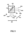
- FIG. 5 is a schematic drawing showing a top plan view of an exemplary reflective region useful in the present invention comprising an enclosed TIR surface.
- FIG. 6 is a schematic drawing showing a top plan view of an exemplary beam array controller of the present invention capable of providing non-equidistant beam array compression.
- FIG. 7 is a schematic drawing showing a top plan view of an exemplary optical configuration of the present invention comprising two beam array controllers optically arranged in series.
- FIG. 8 is a schematic drawing showing a perspective view of an exemplary beam array pitch compressor cartridge of the present invention.
- Beam array refers to a plurality of light beams. Beam arrays comprise pulsed laser beams, continuous wave laser beams, non-laser light beams and all equivalents known in the art. “Parallel beam array” refers to a plurality of light beams propagating along axes that are parallel to a defining axis, such as an input axis or an output axis. “One-dimensional beam array” and “linear beam array” are used synonymously and refer to a series of light beams wherein the propagation axes of the beams are substantially confined to a single plane. Two-dimensional beam arrays are a series of light beams wherein the propagation axes of the beams occupy a plurality of planes. Beam array controllers and pitch compressors of the present invention are capable of selectively adjusting the spacing between beams in one-dimensional or two dimensional beam arrays.
- Beam array controller refers to a device or device component for adjusting the spatial characteristics, optical characteristics or both of a beam array.
- Exemplary beam array controllers of the present invention are capable of, for example, adjusting the propagation axis of individual beams in a beam array, adjusting the brightness and brightness spatial distribution of a beam array, adjusting the pitch of a set of a parallel light beams, and adjusting the photon density of a beam array.
- Beam array controllers of the present invention comprise a means of directing one or more light beams of a beam array to one or more detectors, fiber optic elements, optical couplers, fiber optic devices or photosensitive materials.
- Set of input beams refers to a plurality of light beams.
- Sets of input beams useable in the present invention include one-dimensional beam arrays and two-dimensional beam arrays.
- Sets of input beams useable in the present invention include parallel beam sets or nonparallel beam sets.
- Beam array pitch controller refers to a device or device component for adjusting the pitch of a beam array. Beam array pitch controllers provide a means of increasing or decreasing the spacing between propagation axes of adjacent beams in beam array. Beam array pitch controllers of the present invention are particularly useful for changing the pitch of a parallel beam array.
- Light beam refers to light propagating along a set of propagation axes.
- the set of propagation axes of a light beam includes propagation axes that are preferably proximate to each other.
- the set of propagation axes of a light beam includes axes that are substantially parallel, preferably exhibiting deviations from absolutely parallelisms which are less than 10 degrees.
- the distribution of propagation axes of light in a light beam can be symmetric or asymmetric with respect to one or more defining axes.
- the term light beam is intended to be interpreted consistently with the meaning of this term held by persons skilled in the art of optics and optical devices.
- Light beams useable in an embodiment of the present invention can be collimated, non-collimated, focused or divergent.
- Light beams useable in an embodiment of the present invention can have any shape including, but not limited to, substantially cylindrical shape, substantially conical shape and substantially cuboid shape.
- Light beams useable in the present invention can be generated by a range of optical sources including, but not limited to, laser sources, non-laser sources, lamps, radiating bodies, pulsed light sources, continuous light sources, wide area light sources or any combination of these.
- Planar refers to a spatial characteristic of a surface wherein all points of the surface reside in the same plane. As used herein, the term planar is intended to encompass some deviation from absolutely planar characteristics. Deviations from absolute planar characteristics can be quantified with respect to the angle of a vector extending form the center point of a planar surface to the point deviating from the plane containing the planar surface. Preferred planar surfaces exhibit deviations from absolutely planar characteristics which are less than 50 arcminutes. More preferred planar surfaces exhibit deviations from absolutely planar characteristics which are less than 6 arcminutes.
- Parallel refers to a geometry in which two surfaces are equidistant from each other at all points and have the same direction or curvature.
- the term parallel is intended to encompass some deviation from absolute parallelism.
- Preferred parallel surfaces exhibit deviations from absolute parallelism which are less than 100 arcminutes. More preferred parallel surfaces exhibit deviations from absolute parallelism which are less than 50 arcminutes. Most preferred parallel surfaces exhibit deviations from absolutely absolute parallelism which are less than 5 arcminutes.
- Ultra flat refers to an extent of surface irregularity of a given optical surface with a deviation from average surface position approximately on the order of the light impinging on the surface.
- the spatial frequency of an ultra flat optical surface is smaller than the frequency of light impinging on the surface.
- ultra flat surfaces of the present invention have deviations from average surface position of less than 50 nm.
- Ultra smooth refers to an extent of surface irregularity of a given optical surface wherein the lateral distance between prominent surface features is substantially smaller than the wavelength of light impinging on the surface.
- the spatial frequency of an ultra smooth optical surface is greater than the frequency of light impinging on the surface.
- ultra smooth surfaces of the present invention have deviations from average surface position of less than 1 Angstrom.
- Optical contact refers to a method of bonding two optical elements.
- a preferred method of optical contact coupling comprises the steps of: (1) cleaning and polishing the interface surfaces of the optical elements to be bonded, (2) laying the surfaces together at an optical interface and (3) applying a force to both surfaces such that the air between the interface surfaces is displaced and optical contact is achieved.
- Optical contact is preferred for fabricating beam array controllers and beam array pitch controllers of the present invention because this method does not significantly affect the transmission of light through bonded elements and because this method provides a robust and durable bond between two optical elements.
- optical contact is preferred for some applications because it does not degrade the extent of parallelism achieved between first and second surfaces.
- TIR surface refers to a surface wherein an incident light beam is substantially reflected by total internal reflection. TIR occurs when an incident light beam passes from one material to a second material having an index of refraction less than that of the first material and occurs at incident angles greater than a critical angle defined by the expression:
- ⁇ c the critical angle
- n 1 the refractive index of the first material
- n 2 the refractive index of the second material.
- the first material is SiO 2 and the second material is air at standard temperature and pressure.
- Use of TIR in beam array controllers and pitch controllers of the present invention is preferred in some embodiments because it provides very high reflectivity over a very broad range of wavelengths.
- use of TIR is preferred in some embodiments because it reduces wavelength dependent changes in the phases of s- and p-polarization beam components.
- “Enclosed TIR surface” refers to a TIR surface that is substantially or completely surrounded by one or more enclosing elements.
- Exemplary enclosed TIR surfaces are not exposed to the ambient surroundings.
- An exemplary enclosed TIR surface comprises a TIR cavity disposed on the surface of a substrate which is opposite one or more incident beams.
- the TIR cavity has a lower refractive index than the substrate and is surrounded on the side opposing the substrate by one or more enclosing elements capable of preventing damage to the TIR surface.
- Materials useful for enclosing TIR surfaces include but are not limited to SiO 2 , polymeric materials, plastics, thermoplastics, thermosets, glass, and fused silica.
- the TIR cavity has a thickness that is greater than about three wavelengths corresponding to the wavelength of the incident beam, more preferably greater than about six wavelengths corresponding to the wavelength of the incident beam.
- the substrate is SiO 2 and the TIR cavity is filled with air at standard temperature and pressure.
- Enclosed TIR surfaces are preferred for some applications because the surface providing TIR is protected, and unwanted deposition of material or surface deformation can be effectively minimized or complete avoided.
- the extent of beam array pitch compression can be expressed in terms the ratio of the first pitch of a set of input beams to the second pitch of a set of output beams (P 1 /P 2 ) and “the extent of beam array pitch expansion” can be expressed in terms of the ratio of the second pitch of a set of output beams to the first pitch of a set of input beams (P 2 /P 1 ).
- Optical efficiency refers to the ability of an optical device or device component to transmit a light beam or plurality of light beams with low light losses. Beam array controllers and beam array pitch controllers for some applications have high optical efficiency and transmit at least 95% of incident light. More preferred beam array controllers and beam array pitch controllers for some applications transmit 99.5% of incident light.
- Brightness refers to a property quantifying the intensity of light of an optical source, such as a plurality of light beams. Brightness can be characterized in terms of the energy flux per solid angle per unit of frequency. “Brightness spatial distribution” refers to the distribution of brightness over one or more defining axes, such as a defining axis oriented perpendicular to the propagation axes of a parallel beam array. Beam array controllers and beam array pitch controllers of the present invention provide a means of adjusting the brightness and brightness spatial distribution of a set of input beams.
- Thin film layer refers to a thin film comprising a coating of atoms, molecules or ions or mixtures thereof.
- thin film layers useable in the present invention comprise a single-layer or a plurality of thin film layers.
- Thin film layers useable in the present invention can have either a homogeneous composition or a heterogeneous composition and can comprise a single phase or a plurality of phases.
- Thin film layers of the present invention include but are not limited dielectrics, semiconductors, metals and any combinations of these materials.
- reference to thin dielectric layers in the present invention includes but is not limited to metal oxide, metalloid oxide and salt thin films.
- Metal oxides, metalloid oxides and salts useable in the present invention include but are not limited to Ta 2 O 5 , SiO 2 , HfO 2 , TiO 2 , MgF 2 , CaF 2 , Nb 2 O 5 , glass or mixtures of these materials.
- Thin metalloid and metal layers of the present invention include but are not limited to Si and Al.
- Thin film layers of the present invention can be any size, shape, thickness or optical thickness.
- Thin film layers of the present invention include but are not limited antireflection coatings, partially reflective optical coatings, polarization selective optical coatings, highly reflective coatings, and phase correcting coatings.
- Prism element refers to an optical element or device component having a geometric shape of a prism.
- Prism elements of the present invention can have any prism shape including, but not limited to, cubes, triangular prisms, hexagonal prisms, right prisms, cuboids, pentagonal prisms, octagonal prisms, augmented triangular prisms and augmented cuboids.
- This invention provides beam array controllers for changing the spatial and optical characteristics of a beam array.
- the present invention provides beam array pitch controllers for changing the spacing between adjacent beams in a beam array and for adjusting the brightness and brightness spatial distribution of a beam array.
- FIG. 1 illustrates an exemplary beam array pitch controller having a parallel, dual reflective surface optical geometry, particularly useful for achieving beam compression or expansion by a factor of 2.
- the illustrated pitch controller 100 comprises a first surface 110 in optical communication with second surface 120 .
- Second surface 120 is positioned parallel to the first surface 110 and spaced apart from the first surface by a selected distance, W 130 .
- First surface 110 has a reflective region 140 which extends a selected distance 145 along first surface 110 .
- Second surface 120 has a plurality of reflective regions 150 a , 150 b and 150 c which extend selected lengths 155 a , 155 b and 155 c along second surface 120 , respectively.
- Second surface 120 also has a plurality of transmissive regions 160 a , 160 b and 160 c which extend selected lengths 165 a , 165 b and 165 c along second surface 120 , respectively.
- transmissive surfaces comprise anti-reflection thin film coatings, preferably for some applications having a reflectivity less than 0.5% and more preferably 0.2%
- transmissive surfaces comprise index matched optical cement or optical contact.
- reflective regions 150 a , 150 b and 150 c and transmissive regions 160 a , 160 b and 160 c together comprise an alternating pattern of reflective regions and transmissive regions on second surface 120 .
- FIG. 1 The optical paths of a set of input beams 170 and a set of output beams 172 are also shown in FIG. 1 .
- Input beams 175 a , 175 b , 175 c , 175 d , 175 e and 175 f propagate along optical axes parallel to an input axis 190 and adjacent input beams are separated by a constant, first beam pitch, P 1 195 .
- input beams 175 a , 175 b , 175 c , 175 d , 175 e and 175 f are oriented at angles of incidence 176 equal to 45° from surface normal 177 , with respect to first surface 110 and second surface 120 .
- Input beams 175 a , 175 b and 175 c are reflected by reflective region 140 of first surface 110 and form a first reflected set of output beams 185 a , 185 b , 185 c propagating along optical axes parallel to an output axis 205 .
- Input beams 175 d , 175 e and 175 f are reflected by reflective regions 150 c , 150 b and 150 a , respectively, of second surface 120 and form a second reflected set of output beams 185 d , 185 e , 185 f propagating along optical axes parallel to an output axis 205 .
- First reflected set of output beams 185 a , 185 b , 185 c are transmitted through transmissive regions 160 c , 160 b and 160 a , respectively, of second surface 120 and combine with second reflected set of output beams 185 d , 185 e , 185 f to form a set of output beams 172 propagating along optical axes parallel to an output axis 205 .
- Adjacent output beams 172 are separated by a constant, second beam pitch, P 2 220 , which is different than first pitch, P 1 195 .
- P 2 220 is equal to one half of P 1 195 .
- reflective regions 150 a , 150 b and 150 c extend distances 155 a , 155 b and 155 c along second surface 120 selected to provide substantially complete reflection of all portions of input beams 175 d , 175 e and 175 f . In this embodiment, therefore, distances 155 a , 155 b and 155 c are principally determined by the beam diameters of input beams 175 d , 175 e and 175 f .
- transmissive regions 160 a , 160 b and 160 c extend lengths 165 a and 165 b selected to provide substantially complete transmission of all portions of input beams 175 a , 175 b and 175 c and, therefore, are principally governed by the beam diameters of the input beams 175 a , 175 b and 175 c .
- Reflective region 140 extends a distance 145 along first surface 110 selected to provide substantially complete reflection of all portions of input beams 175 a , 175 b and 175 c .
- first surface 110 has a plurality of reflective regions for providing substantially complete reflection of input beams 175 a , 175 b and 175 c .
- first surface has one or more transmissive regions, non-transmissive regions, absorbing regions, scattering regions or any combination of these.
- second surface can comprise one or more non-transmissive regions, absorbing regions, scattering regions or any combination of these.
- Reflective regions useable in the present invention include planar reflective surfaces, curved reflective surfaces or combinations of these. Use of curved reflective surfaces in the present invention is beneficial for applications requiring focusing or collimation of input beams and/or output beams.
- alternating reflective regions and transmissive regions of the present invention comprise a symmetric pattern on second surface 120 or an asymmetric pattern on second surface 120 .
- FIG. 2 shows the exemplary beam array pitch controller 100 upon changing the angles of incidence 176 of set of input beams 170 to equal to 55° from surface normal 177 with respect to first surface 110 and second surface 120 .
- Similar beam array compression is also achieved for this angle of incidence.
- Variation of the angles of incidence substantially affects the spatial orientation of the output axis 205 relative to input axis 190 .
- increasing the angles of incidence increases the corresponding angles of reflection for beams 175 a , 175 b , 175 c , 175 d , 175 e and 175 f resulting in a larger angle between input axis 190 and output optical axis 205 .
- variation of the angle of incidence in this embodiment comprises a means of selectively adjusting the orientation of the propagation axes of output beams.
- the ability to control orientation of the propagation axes of the output beams is beneficial because it provides a means of directing the output beams onto photosensitive materials, optical coupling devices and/or detectors.
- Preferred embodiments of the present invention are capable of efficiently compressing or expanding input beams having angles of incidence selected over the range of about 25° to about 65° from surface normal with respect to first surface 110 and second surface 120 .
- the methods of the present invention include the use of focusing and collimating elements to control input beam diameters and facilitate transmission of input beams and reflected input beams through transmissive regions 160 a , 160 b and 160 c.
- beam array controller 100 of the present invention also provides for beam array expansion. Specifically, beam expansion is provided by reversing the input and output axes shown in FIGS. 1 and 2 . For example, directing a set of input beams along output axis 205 will yield first and second sets of reflected output beams which combine in a manner providing beam array expansion. Accordingly, beam pitch controllers of the present invention are capable of providing either pitch compression or pitch expansion functionality dependent upon a selection of the appropriate orientation of the propagation axes of the set of input beams.
- the distance 130 separating first and second surfaces is selected to provide optimal beam transmission for a selected angle of incidence and extent of beam array compression or expansion.
- the distance separating first and second surfaces is governed by the equation:
- W P 1 ⁇ ⁇ ( N - 1 ) ⁇ Cos ⁇ ⁇ ( ⁇ I ) Sin ⁇ ⁇ ( 2 ⁇ ⁇ I ) M ( II )
- W is the distance between first and second parallel surfaces
- ⁇ 1 is the angle of incidence relative to surface normal
- N is the number of beams in the set of input beams
- P 1 is the spacing between the propagation axes of adjacent beams in the input beam set (i.e. the pitch of the input beam set)
- the distance separating first and second parallel surfaces is governed by the equation:
- W P 1 ⁇ ⁇ ( N ) ⁇ Cos ⁇ ⁇ ( ⁇ I ) Sin ⁇ ⁇ ( 2 ⁇ ⁇ I ) M ( III ) wherein W, ⁇ 1 , N, P 1 and M are as defined above with respect to equation II.
- an exemplary beam pitch controller having a dual reflective surface geometry is configured to provide an extent of compression or expansion equal to 2.
- first and second surfaces are separated by a distance of 0.84 inch to provide beam array compression by a factor of two for a set of 6 parallel input beams having a 0.5 inch equidistant beam spacing and oriented at angles of incidence of 45° from surface normal with respect to first and second surfaces.
- the present invention includes beam array pitch controllers providing a fixed extent of beam array compression or expansion for a selected angle of incidence.
- FIG. 3 illustrates an exemplary optical geometry for a beam array pitch controller capable of providing a fixed extent of beam array compression or expansion.
- the illustrated beam array pitch controller further comprises an alignment spacer 250 which is capable of maintaining a selected distance between first surface 110 and second surface 120 .
- first surface 110 is an internal side 251 of a first prism element 256 and second surface 120 is an internal side 253 of second prism element 258 .
- beam input surfaces 262 and beam output surface 264 of alignment spacer 250 and second prism element 258 have anti-reflection coatings to minimize unwanted reflections at these surfaces and to provide optically efficient beam pitch control.
- Alignment spacer 250 has a thickness 260 selected to provide a desired extent of compression or expansion for a selected angle of incidence and number of input beams. Alignment spacer 250 is in operational contact with first prism element 256 and second prism element 258 . Preferred alignment spacers of the present invention do not significantly absorb ( ⁇ 1% absorption) the input or reflected beams and do not substantially affect the polarization states of input or reflected beams.
- Operational contact of alignment spacer 250 , first prism element 256 and second prism element 258 can be provided by any means known in the art including, but not limited to, the use of optical contact bonding, optical adhesive or optical cement.
- Optical contact bonding is preferred for some applications because it is capable of providing a durable bond between alignment spacer 250 , first prism element 256 and second prism element 258 without substantially degrading the transmission properties of the beam array pitch controller.
- An advantage of the illustrated design is that it allows for piece-by-piece assembly wherein reflective surfaces and transmissive surfaces on first and second prism elements are separately fabricated and subsequently operationally coupled to the alignment spacer.
- first surface 110 and second surface 120 are parallel first side 252 and second side 254 , respectively, of alignment spacer 250 .
- first prism element 256 and second prism element 258 are operationally coupled to alignment spacer 250 to form protective layers shielding first and second surfaces from the ambient surroundings.
- the pitch controllers of the present invention also provide a means of reordering of light beams comprising a set of input beams.
- the output beams 185 a , 185 b , 185 c , 185 d , 185 e , 185 f generated by this embodiment reflect a reordering of input beams 175 a , 175 b , 175 c , 175 d , 175 e and 175 f to a new sequence corresponding to 175 a , 175 d , 175 b , 175 e , 175 c and 175 f .
- Beam array reordering provided by the present invention is useful for directing selected light beams in a beam array onto selected directors, beam coupling devices, fiber optic elements, or fiber optic devices.
- beam array pitch controllers of the present invention further comprise one or more additional surfaces having a plurality of alternating reflective regions and transmissive regions.
- FIG. 4 illustrates an exemplary beam array pitch controller having an additional surface having a plurality of alternating reflective regions and transmissive regions, particularly useful for realizing beam compression or expansion by a factor of 3.
- the illustrated pitch controller 300 further comprises a third surface 310 which is positioned parallel to the first surface 110 and spaced apart from the first surface by a selected distance, X 320 .
- the distance separating first surface 110 and second surface 120 is equal to the distance separating second surface 120 and third surface 310 .
- Third surface 310 has a plurality of reflective regions 350 a and 350 b which extend selected lengths 355 a and 355 b , respectively, along third surface 310 .
- Third surface also has a plurality of transmissive regions 357 a and 357 b which extend selected lengths 358 a and 358 b , respectively, along third surface 310 .
- a set of input beams 170 are directed at first, second and third surfaces and generate first, second and third reflected sets of output beams. Combination of first, second and third reflected sets of output beams generates a set of output beams 372 propagating along optical axes parallel to an output axis 205 .
- Output beams 372 are separated by a constant, second beam pitch, P 2 380 , which is different than first pitch, P 1 195 .
- P 2 380 is equal to one third of P 1 195 .
- an input beam comprising 6 beams having a pitch equal to 1 inch is compressed by a factor of 3.
- the present invention includes embodiments have a plurality of additional surfaces having alternating reflective regions and transmissive regions.
- Use of additional surfaces having alternating reflective regions and transmissive regions in the present invention is particularly beneficial for providing a larger extent of beam array pitch compression or expansion than embodiments having a dual parallel, reflective surface optical geometry.
- the present invention includes beam array pitch compressors for adjusting the pitch of a two-dimensional beam array.
- the input beams comprise an array of input light beams, preferably parallel input beams, positioned along multiple defining axes which are orthogonal to input axis 190 .
- Beam sets interact with first and second surfaces to provide beam array compression or expansion in at least one of the one dimensions defining the two-dimensional array.
- Reflective regions in the present invention can comprise any surface, optical coating, plurality of optical coatings or optical element which provides high reflectivity, preferably for some applications reflectivity greater than 90% reflectivity and more preferably for some applications greater than 99% reflectivity.
- Exemplary reflective regions of the present invention comprise one or more thin film layers including but not limited, to dielectric film layers, semiconductor layers, metal layers or any combination of these.
- Exemplary thin film reflective regions of the present invention have a number of thin film layers selected from the range of about 1 to about 50 thin film layers. Use of thin film layers comprising a plurality of thin dielectric films having alternating high and low indices of refraction is preferred for applications requiring high optical efficiency because they reflect light very efficiently with minimal absorption, preferably less than 1% absorption.
- Thin film layer reflective regions of the present invention can be fabricated by deposition methods, particularly sputtering deposition methods, and lithography techniques well known in the art of the fabrication of optical devices.
- reflective regions of the present invention comprise total internal reflection (TIR) surfaces.
- TIR surfaces are particularly advantageous for certain applications.
- embodiments of the present invention including TIR surfaces provide highly versatile beam array controllers and pitch controllers, which are capable of efficiently controlling beam arrays corresponding to wide range of light sources and a wide range of wavelengths because TIR surfaces exhibit high reflectivity over a broad range of wavelengths of light, preferably for some applications reflectivities greater than 99% over a wave length range of at least 300 nm.
- use of TIR surfaces in the present invention is beneficial for applications requiring the polarization scheme of input beams to be maintained because the phase change between s- and p-polarization components is minimized in TIR.
- TIR surfaces can be coated with one or more thin film coatings to further minimize or control the phase difference between s- and p-polarization components upon reflection.
- TIR surface are compatible with high intensity light beams, such as diode laser light beams, and thus, can provide high optical efficiency for applications involving high intensity light beams.
- FIG. 5 shows a top plan view of exemplary reflective region useful in the present invention comprising an enclosed TIR surface.
- the enclosed TIR surface 400 comprises substrate 405 operationally coupled to an enclosing element 410 .
- TIR cavity 415 is formed between enclosed TIR surface 420 of substrate 405 and enclosing element 410 .
- TIR cavity 415 can be any shape which provides substantial total internal reflection, including cuboid shaped.
- Enclosed TIR cavity extends a selected length 425 along substrate 405 and has a selected thickness 430 . Thickness 430 is preferably great enough to avoid the occurrence of frustrated total internal reflection.
- thickness 430 is greater than about 3 wavelengths corresponding to the wavelength of light of an incident beam, more preferably greater than about 6 wavelengths of light of an incident beam.
- Length 425 is preferably large enough to reflect substantially all of an incident beam or plurality of incident beams.
- TIR surface 420 is ultra flat, ultra smooth and completely enclosed by enclosing element 410 .
- Use of ultra flat and ultra smooth surfaces for total internal reflection is beneficial for providing high reflectivity and avoiding diffuse reflection.
- TIR cavity 415 is filled with air at standard temperature and pressure and substrate 405 is SiO 2 .
- the TIR cavity can comprise any material or plurality of materials having a lower index of refraction than that of substrate 405 .
- TIR cavity is filled with a gas or plurality of gases, is a vacuum or comprises a dielectric material having an index of refraction less than that of substrate 405 .
- Substrate 405 can have any shape which includes a flat and smooth TIR surface 420 and can comprise any material having a larger index of refraction than that of TIR cavity 415 .
- Enclosing element 410 can comprise any material capable of surrounding and protecting enclosed TIR surface 420 including, but not limited to, dielectric materials, polymeric materials, plastics, thermoplastics, thermosets, glass, semiconductor materials and metals. Preferred enclosing elements 410 include a unitary piece of SiO 2 or polymeric material having a cavity volume removed therein.
- TIR cavities of the present invention can be fabricated by any material removal method including sonic milling, surface grinding or chemical etching. In addition, TIR cavities of the present invention can also be produced by building up the material around the cavity using spacers or thin film coatings. The positioning and dimensions of the cavity can be precisely controlled using either photoresists patterning or CNC machining.
- incident beams 435 a , 435 b and 435 c are directed onto enclosed TIR surface 420 and are substantially reflected by total internal reflection.
- incident beams 435 a , 435 b and 435 c in FIG. 5 are oriented at angles of incidence equal to 45°, the enclosed TIR surfaces of the present invention are capable of use with other incident beam orientations that are greater than the critical angle required to generate TIR.
- the enclosed TIR optical geometry of the present invention is beneficial for several reasons.
- enclosing element 410 protects the TIR surface 420 , thereby, preventing degradation due to deposition of materials on to TIR surface 420 .
- enclosing element 410 also serves to preventing deformation of the surface by physical and chemical processes such as scratching, denting, chipping or etching.
- use of enclosed TIR surfaces is advantageous because the optical geometry of these surfaces places fewer limitations on the overall optical geometry of the optical components than conventional exposed TIR surfaces. Therefore, enclosed TIR surfaces are capable of convenient and easy integrated into complex optical devices, such as the beam array controllers and pitch controllers of the present invention.
- the present invention also comprises beam array controllers which are capable of generating a plurality of output beams wherein adjacent output beams are not evenly spaced.
- FIG. 6 shows an exemplary beam array controller 500 of the present invention capable of providing non-equidistant beam array compression.
- a set of parallel input beams 510 having a constant pitch is directed at first surface 515 and second surface 520 of the illustrate beam array controller.
- Reflective regions 525 a , 525 b and 525 c and transmissive regions 530 a , 530 b and 530 c of second surface 520 are positioned such that output beams 535 comprise three discrete beam pairs 540 a , 540 b and 540 c , which are separated by distance 550 .
- Beam array controllers of the present invention capable of providing non-equidistant beam array compression are useful for separating a set of input beams into spatially segregated beam sub-groups.
- beam array controllers of the present invention capable of providing non-equidistant beam array compression are useful transforming a symmetrically spaced input beam set into an asymmetrically spaced output beam set.
- a plurality of beam array controllers and pitch compressors of the present invention are operationally coupled in series to precisely manipulate the spatial and/or optical characteristics of a beam array.
- FIG. 7 shows an exemplary optical geometry of the present invention comprising two beam array controllers optically arranged in series, particularly useful for realizing beam array pitch compression or expansion by a factor of 4.
- the exemplary optical geometry 600 comprises first beam array controller 610 in optical communication with second beam array controller 620 .
- Set of 6 input beams 625 having a first pitch, P 1 is directed on first beam array controller 610 and undergoes non-equidistant beam array compression generating a set of output beams comprising three discrete beam pairs 630 a , 630 b and 630 c .
- Discrete beam pairs 630 a , 630 b and 630 c are subsequently directed onto second beam array controller 620 wherein beam pairs undergo pitch compression to generate a set of 6 output beams 640 having a second pitch, P 2 , wherein P 2 P 1 .
- the optical geometry shown in FIG. 7 is capable of generating a second pitch which is equal to one fourth of the first pitch, P 1 .
- first and second surfaces of the first beam array controller 610 are separated by a distance of 0.972 inch and first and second surfaces of the second beam array controller 620 are separated by a distance of 0.530 inch.
- beam array controllers and beam array pitch controllers of the present invention are arranged in parallel.
- the exemplary embodiment shown in FIG. 7 is but one means of combining one or more beam array controllers of the present invention. All possible other combinations and methods of coupling beam controllers and pitch compressors in series are within the scope of the present invention.
- Beam array controllers and beam array pitch controllers of the present invention can be used a stand alone optical component or can be a device component in an integrated optical device.
- a beam array pitch compressor of the present invention comprises a cartridge which can be easily integrated into an optical system, such as a diode laser bar array light sources or plurality of wide area emitter sources.
- FIGS. 8A and 8B are schematic drawings showing an exemplary beam array pitch compressor cartridge 800 , particularly well suited for efficient optical coupling to a plurality of linear bar array optical sources. As shown in FIG. 8A , mounting system 810 is provided for incorporating the beam array pitch compressor cartridge 800 into an integrated optical device.
- Mounting system 810 can comprise any system capable of effectively engaging and securing beam array pitch compressor cartridge 800 including, but not limited to, the use of set screws, braces, clamps, selectively adjustable optical positioners, nuts, bolts, latches, rivets and other equivalents well-known in the art.
- FIG. 8B shows a set of input beams 820 (individually 825 a , 825 b , 825 c , 825 d , 825 e , 825 f and 825 g ) which can be a two-dimensional beam array comprising seven separate linear (one-dimensional) beam arrays or can be light beams generated by a plurality of wide area emitters.
- beam array pitch compressor cartridge 800 changes the spacing along pitch adjustment axes 830 between individual linear beam arrays or individual light beams generated by a plurality of wide area emitters.
- Beam array controllers and pitch compressors of the present invention are compatible with input beams having wide variety of optical and spatial characteristics.
- the present invention includes methods and devices for controlling a set of parallel or non-parallel input beams.
- Input beams controllable by the present invention can be symmetrically disposed along an axis perpendicular to their propagation axes or can be asymmetrically arranged.
- the present invention includes methods and devices for controlling input beams having very high intensities.
- the beam array controllers and pitch compressor of the present invention can control light beams from a wide range of sources including but not limited to, pulse lasers, continuous wave lasers, diode laser bar arrays, Nd:YAG lasers, HeNe lasers, excimer lasers, gas lasers, solid state lasers, wide area emitter optical sources and non-laser light sources.
- the methods and devices of the present invention can accommodate a set of input beams comprising any number of individual beams.
- the beam array controllers and pitch compressors of the present invention are configured to receive a number of input beams selected over the range of about 5 to about 30 input beams.
- the present invention includes methods of manipulating the brightness spatial distribution of a beam array, preferably a parallel beam array.
- a beam array By decreasing the spacing between adjacent beams in a beam array the brightness of a beam array is capable of being selectively increased, and by increasing the spacing between adjacent beams in a beam array the brightness of a beam array is capable of being selectively decreased.
- Beam array controllers and pitch compressors of the present invention are capable of selectively manipulating the brightness spatial distribution of a plurality of beams.
- beam array controllers and pitch compressors of the present invention are capable of adjusting the brightness spatial distribution of a beam array along a defining axis oriented orthogonal to the propagation axes of the light beams in the array.
- Beam array controllers and beam array pitch controllers of the present invention can comprise device components in a variety of optical devices including but not limited to light sources, lasers, optical signal generators, light filters, detectors, fiber optic routing devices, optical alignment systems, add/drop filters and interferometers. Beam array controllers and beam array pitch controllers of the present invention can be directly or indirectly operationally coupled to a variety of devices including but not limited to focusing elements, collimating elements, lasers, detectors, reflectors, polarizers, interference filters, fiber optic couplers, light sources, temperature controllers, temperature sensors and optical sources. Beam array controllers and beam array pitch controllers of the present invention can be used separately to provide beam array control or a series of the beam array controllers and beam array pitch controllers of the present invention can be used to provide beam array control.
Abstract
Description
wherein θc is the critical angle, n1 is the refractive index of the first material and n2 is the refractive index of the second material. In one embodiment, the first material is SiO2 and the second material is air at standard temperature and pressure. Use of TIR in beam array controllers and pitch controllers of the present invention is preferred in some embodiments because it provides very high reflectivity over a very broad range of wavelengths. In addition, use of TIR is preferred in some embodiments because it reduces wavelength dependent changes in the phases of s- and p-polarization beam components. “Enclosed TIR surface” refers to a TIR surface that is substantially or completely surrounded by one or more enclosing elements. Exemplary enclosed TIR surfaces are not exposed to the ambient surroundings. An exemplary enclosed TIR surface comprises a TIR cavity disposed on the surface of a substrate which is opposite one or more incident beams. The TIR cavity has a lower refractive index than the substrate and is surrounded on the side opposing the substrate by one or more enclosing elements capable of preventing damage to the TIR surface. Materials useful for enclosing TIR surfaces include but are not limited to SiO2, polymeric materials, plastics, thermoplastics, thermosets, glass, and fused silica. In a preferred embodiment, the TIR cavity has a thickness that is greater than about three wavelengths corresponding to the wavelength of the incident beam, more preferably greater than about six wavelengths corresponding to the wavelength of the incident beam. In a preferred embodiment, the substrate is SiO2 and the TIR cavity is filled with air at standard temperature and pressure. Enclosed TIR surfaces are preferred for some applications because the surface providing TIR is protected, and unwanted deposition of material or surface deformation can be effectively minimized or complete avoided.
wherein W is the distance between first and second parallel surfaces, θ1 is the angle of incidence relative to surface normal, N is the number of beams in the set of input beams, P1 is the spacing between the propagation axes of adjacent beams in the input beam set (i.e. the pitch of the input beam set), and M is the extent of compression or expansion (M=P1/P2, where P2 is the pitch of the set of output beams). For an input beam set comprising an odd number of parallel beams, the distance separating first and second parallel surfaces is governed by the equation:
wherein W, θ1, N, P1 and M are as defined above with respect to equation II.
Claims (30)
Priority Applications (1)
| Application Number | Priority Date | Filing Date | Title |
|---|---|---|---|
| US10/885,297 US7023620B1 (en) | 2003-07-03 | 2004-07-01 | Beam array pitch controller |
Applications Claiming Priority (2)
| Application Number | Priority Date | Filing Date | Title |
|---|---|---|---|
| US48552903P | 2003-07-03 | 2003-07-03 | |
| US10/885,297 US7023620B1 (en) | 2003-07-03 | 2004-07-01 | Beam array pitch controller |
Publications (1)
| Publication Number | Publication Date |
|---|---|
| US7023620B1 true US7023620B1 (en) | 2006-04-04 |
Family
ID=36102009
Family Applications (1)
| Application Number | Title | Priority Date | Filing Date |
|---|---|---|---|
| US10/885,297 Active US7023620B1 (en) | 2003-07-03 | 2004-07-01 | Beam array pitch controller |
Country Status (1)
| Country | Link |
|---|---|
| US (1) | US7023620B1 (en) |
Cited By (8)
| Publication number | Priority date | Publication date | Assignee | Title |
|---|---|---|---|---|
| US20050115938A1 (en) * | 2003-11-13 | 2005-06-02 | Kazushige Sawaki | Laser processing apparatus and laser processing method |
| US20150136755A1 (en) * | 2011-11-04 | 2015-05-21 | Applied Materials, Inc. | Optical design for line generation using microlens array |
| US9485046B1 (en) | 2013-04-12 | 2016-11-01 | Alliance Fiber Optic Products, Inc. | Optical spot array pitch compressor |
| US20180292070A1 (en) * | 2015-04-29 | 2018-10-11 | Appotronics Corporation Limited | Light guide component and light source device |
| CN111538114A (en) * | 2019-02-06 | 2020-08-14 | 浜松光子学株式会社 | Optical element |
| CN111708174A (en) * | 2020-06-18 | 2020-09-25 | 武汉光迅科技股份有限公司 | Spectroscopic lens group and spectroscopic probe |
| CN113132576A (en) * | 2019-12-31 | 2021-07-16 | 华为技术有限公司 | Camera shooting method, camera shooting module and electronic equipment |
| WO2024015554A1 (en) * | 2022-07-15 | 2024-01-18 | Quantinuum Llc | Spatial period converter with monolithic zoom |
Citations (66)
| Publication number | Priority date | Publication date | Assignee | Title |
|---|---|---|---|---|
| US4204771A (en) | 1978-05-08 | 1980-05-27 | Arthur Shull | Tuning of etalons |
| US4566765A (en) * | 1982-10-15 | 1986-01-28 | Hitachi, Ltd. | Apparatus for summing several ring-shape laser beams |
| US4636075A (en) | 1984-08-22 | 1987-01-13 | Particle Measuring Systems, Inc. | Particle measurement utilizing orthogonally polarized components of a laser beam |
| US4756602A (en) | 1987-06-05 | 1988-07-12 | Rockwell International Corporation | Narrowband optical filter with partitioned cavity |
| US4798465A (en) | 1986-04-14 | 1989-01-17 | Particle Measuring Systems, Inc. | Particle size detection device having high sensitivity in high molecular scattering environment |
| US4813756A (en) | 1988-01-25 | 1989-03-21 | Bell Communications Research, Inc. | Etalon filters for optical channel selection in wavelength division multiplexed fiber systems |
| US5037180A (en) | 1990-07-19 | 1991-08-06 | At&T Bell Laboratories | Optical filter on optical fiber end face |
| US5085500A (en) | 1989-11-28 | 1992-02-04 | Tsi Incorporated | Non-imaging laser particle counter |
| US5121988A (en) | 1989-10-04 | 1992-06-16 | Tsi Incorporated | Single particle detector method and apparatus utilizing light extinction within a sheet of light |
| US5155623A (en) | 1988-09-23 | 1992-10-13 | At&T Bell Laboratories | Arrangement for imaging multiple arrays of light beams |
| US5212584A (en) | 1992-04-29 | 1993-05-18 | At&T Bell Laboratories | Tunable etalon filter |
| US5291332A (en) | 1992-03-25 | 1994-03-01 | Hughes Aircraft Company | Etalons with dispersive coatings |
| US5331404A (en) | 1992-11-30 | 1994-07-19 | The United States Of America As Represented By The Secretary Of The Navy | Low noise fiber gyroscope system which includes excess noise subtraction |
| US5400179A (en) | 1992-02-18 | 1995-03-21 | Asahi Kogaku Kogyo Kabushiki Kaisha | Optical multilayer thin film and beam splitter |
| WO1995009354A1 (en) | 1993-09-27 | 1995-04-06 | Venturedyne Limited | Improved particle sensor and method for assaying a particle |
| US5410431A (en) | 1993-06-01 | 1995-04-25 | Rockwell International Corporation | Multi-line narrowband-pass filters |
| US5467189A (en) | 1993-01-22 | 1995-11-14 | Venturedyne, Ltd. | Improved particle sensor and method for assaying a particle |
| US5633724A (en) * | 1995-08-29 | 1997-05-27 | Hewlett-Packard Company | Evanescent scanning of biochemical array |
| US5646786A (en) | 1995-03-24 | 1997-07-08 | Eastman Kodak Company | Beamsplitter for laser multi-beam printers and recorders |
| US5719989A (en) | 1995-06-28 | 1998-02-17 | Jds Fitel Inc. | Multilayer thin film bandpass filter |
| US5751422A (en) | 1996-02-26 | 1998-05-12 | Particle Measuring Systems, Inc. | In-situ particle detection utilizing optical coupling |
| US5781268A (en) | 1996-04-09 | 1998-07-14 | Board Of Regents Of The University Of Colorado | Polarization-insensitive fabry-perot tunable filter |
| US5798859A (en) | 1995-07-27 | 1998-08-25 | Jds Fitel Inc. | Method and device for wavelength locking |
| US5805781A (en) | 1994-12-07 | 1998-09-08 | Hewlett-Packard Company | Printer method and apparatus for combining sub-images to eliminate image artifacts |
| US5825552A (en) | 1995-03-24 | 1998-10-20 | Eastman Kodak Company | Beamsplitter/staggerer for multi-beam laser printers |
| US5828689A (en) | 1996-07-20 | 1998-10-27 | Northern Telecom Limited | Etalon arrangement |
| US5872624A (en) | 1997-06-05 | 1999-02-16 | Gn Nettest (New York) | Method and apparatus for retroreflectively reducing coherence/polarization noise in reflectometers |
| US5926317A (en) | 1996-11-06 | 1999-07-20 | Jds Fitel Inc. | Multilayer thin film dielectric bandpass filter |
| US5999320A (en) | 1995-07-26 | 1999-12-07 | Fujitsu Limited | Virtually imaged phased array as a wavelength demultiplexer |
| US6005995A (en) | 1997-08-01 | 1999-12-21 | Dicon Fiberoptics, Inc. | Frequency sorter, and frequency locker for monitoring frequency shift of radiation source |
| WO2000025154A1 (en) | 1998-10-28 | 2000-05-04 | Coherent, Inc. | Multilayer mirrors dispersion control |
| US6061132A (en) | 1998-07-20 | 2000-05-09 | Pacific Scientific Instruments Company | Dual detector array with noise cancellation for a particle size detection device |
| US6122043A (en) | 1996-06-06 | 2000-09-19 | Gn Nettest (New York) Inc. | Method and apparatus for electrically reducing coherence/polarization noise in reflectometers |
| US6154318A (en) | 1998-08-18 | 2000-11-28 | Coherent, Inc. | Group-delay-dispersive multilayer-mirror structures and method for designing same |
| US6169604B1 (en) | 1999-02-10 | 2001-01-02 | Avanex Corporation | Nonlinear interferometer for fiber optic dense wavelength division multiplexer utilizing a phase bias element to separate wavelengths in an optical signal |
| US6169626B1 (en) | 1999-06-29 | 2001-01-02 | E-Tek Dynamics | Optical signal interleaver |
| US6185168B1 (en) | 1995-03-27 | 2001-02-06 | Matsushita Electric Industrial Co., Ltd. | Super-resolution optical head apparatus |
| US6186937B1 (en) | 1999-07-30 | 2001-02-13 | Lucent Technologies, Inc. | Method and device for obtaining a desired phase of optical characteristic of a fabry-perot etalon |
| US6201907B1 (en) | 1998-06-26 | 2001-03-13 | Jds Fitel Inc. | Optical drop circuit having group delay compensation |
| US6208444B1 (en) | 1996-10-29 | 2001-03-27 | Chorum Technologies Inc. | Apparatus for wavelength demultiplexing using a multi-cavity etalon |
| EP1098212A1 (en) | 1999-11-05 | 2001-05-09 | JDS Uniphase Inc. | Tunable dispersion compensator |
| US6241397B1 (en) | 1998-04-17 | 2001-06-05 | Micron Optics, Inc. | Cascaded fixed and tunable multiple-fiber Fabry Perot filters and fixed and tunable ferrule alignment fixtures for fiber Fabry Perot filters |
| US6249350B1 (en) | 1996-08-05 | 2001-06-19 | Deutsche Telekom Ag | Interferometer and methods for compensation of dispersion or increase in spectral resolution of such an interferometer |
| US6252716B1 (en) | 1999-07-22 | 2001-06-26 | Jds Uniphase Photonics C.V. | Bulk optic interleaver |
| US6263128B1 (en) | 1999-06-02 | 2001-07-17 | Wavesplitter Technologies, Inc. | Fiber unbalanced Mach-Zehnder interferometers with flat-top spectral response for application in wavelength division multiplexers |
| US6275322B1 (en) | 1999-06-08 | 2001-08-14 | Jds Uniphase Corporation | Michelson phase shifter interleaver/deinterleavers |
| US6304689B1 (en) | 1998-01-09 | 2001-10-16 | Communications Research Laboratory Ministry Of Posts And Telecommunications | General multi-function optical filter |
| US6317251B1 (en) | 1996-02-05 | 2001-11-13 | Corning Applied Technologies Corporation | Thin film electro-optic beam steering device |
| US6320663B1 (en) | 1999-01-22 | 2001-11-20 | Cymer, Inc. | Method and device for spectral measurements of laser beam |
| US6373620B1 (en) | 1996-02-05 | 2002-04-16 | Corning Applied Technologies Corporation | Thin film electro-optic beam steering device |
| US6379984B1 (en) | 1999-12-17 | 2002-04-30 | Research Electro-Optics, Inc. | High-precision etalon device and method of construction |
| US6386718B1 (en) | 2001-03-02 | 2002-05-14 | Charles X. W. Qian | Phase and free spectra range adjustable optical reflectors for dense wavelength division multiplexing applications |
| US6414754B1 (en) | 2000-03-08 | 2002-07-02 | Pacific Scientific Instruments Company | Method and apparatus for suppressing stray light in particle detectors |
| US20020126354A1 (en) | 2001-01-19 | 2002-09-12 | Gazillion Bits, Inc. | Optical interleaving with enhanced spectral response and reduced polarization sensitivity |
| US20020154314A1 (en) | 2001-02-27 | 2002-10-24 | Nigel Copner | Athermal interferometer |
| US20020180981A1 (en) | 2001-05-30 | 2002-12-05 | Jds Uniphase Corporation | Multi-cavity resonator interferometer |
| US6570711B2 (en) | 2000-08-01 | 2003-05-27 | Jds Uniphase Inc. | Virtual waveplate and optical channel interleaver formed therewith |
| US6631033B1 (en) | 1999-01-29 | 2003-10-07 | Qinetiq Limited | Multilayer optical filters |
| WO2004006754A2 (en) | 2002-07-16 | 2004-01-22 | Research Electro-Optics, Inc. | Method for noise cancellation by spectral flattening of laser output in a multi-line-laser instrument |
| WO2004007017A2 (en) | 2002-07-16 | 2004-01-22 | Research Electro-Optics, Inc. | Method of noise cancellation in an unpolarized-laser instrument |
| US6683721B2 (en) | 2001-02-27 | 2004-01-27 | Jds Uniphase Corporation | Low dispersion interleaver |
| US20040042083A1 (en) | 2002-08-30 | 2004-03-04 | Turner Nelson C. | Fabry-perot etalon with independently selectable resonance frequency and free spectral range |
| US6725322B1 (en) | 1999-02-22 | 2004-04-20 | Renesas Technology Corp. | Memory card, method for allotting logical address, and method for writing data |
| US6724789B2 (en) | 2000-12-14 | 2004-04-20 | Sri International | Dense wavelength division multiplexing (DWDM) fiberoptic source |
| US20040080834A1 (en) | 2002-10-25 | 2004-04-29 | Thompson James Tristan | Optical interference filter having parallel phase control elements |
| US6913706B2 (en) * | 2002-12-28 | 2005-07-05 | Intel Corporation | Double-metal EUV mask absorber |
-
2004
- 2004-07-01 US US10/885,297 patent/US7023620B1/en active Active
Patent Citations (76)
| Publication number | Priority date | Publication date | Assignee | Title |
|---|---|---|---|---|
| US4204771A (en) | 1978-05-08 | 1980-05-27 | Arthur Shull | Tuning of etalons |
| US4566765A (en) * | 1982-10-15 | 1986-01-28 | Hitachi, Ltd. | Apparatus for summing several ring-shape laser beams |
| US4636075A (en) | 1984-08-22 | 1987-01-13 | Particle Measuring Systems, Inc. | Particle measurement utilizing orthogonally polarized components of a laser beam |
| US4798465B1 (en) | 1986-04-14 | 1991-09-17 | Particle Measuring Syst | |
| US4798465A (en) | 1986-04-14 | 1989-01-17 | Particle Measuring Systems, Inc. | Particle size detection device having high sensitivity in high molecular scattering environment |
| US4893928A (en) | 1986-04-14 | 1990-01-16 | Particle Measuring Systems, Inc. | Highly sensitive particle size detection device having noise cancellation |
| US4798465B2 (en) | 1986-04-14 | 1994-08-30 | Particle Measuring Syst | Particle size detection device having high sensitivity in high molecular scattering environment |
| US4756602A (en) | 1987-06-05 | 1988-07-12 | Rockwell International Corporation | Narrowband optical filter with partitioned cavity |
| US4813756A (en) | 1988-01-25 | 1989-03-21 | Bell Communications Research, Inc. | Etalon filters for optical channel selection in wavelength division multiplexed fiber systems |
| US5155623A (en) | 1988-09-23 | 1992-10-13 | At&T Bell Laboratories | Arrangement for imaging multiple arrays of light beams |
| US5121988A (en) | 1989-10-04 | 1992-06-16 | Tsi Incorporated | Single particle detector method and apparatus utilizing light extinction within a sheet of light |
| US5085500A (en) | 1989-11-28 | 1992-02-04 | Tsi Incorporated | Non-imaging laser particle counter |
| US5037180A (en) | 1990-07-19 | 1991-08-06 | At&T Bell Laboratories | Optical filter on optical fiber end face |
| US5400179A (en) | 1992-02-18 | 1995-03-21 | Asahi Kogaku Kogyo Kabushiki Kaisha | Optical multilayer thin film and beam splitter |
| US5291332A (en) | 1992-03-25 | 1994-03-01 | Hughes Aircraft Company | Etalons with dispersive coatings |
| US5212584A (en) | 1992-04-29 | 1993-05-18 | At&T Bell Laboratories | Tunable etalon filter |
| US5331404A (en) | 1992-11-30 | 1994-07-19 | The United States Of America As Represented By The Secretary Of The Navy | Low noise fiber gyroscope system which includes excess noise subtraction |
| US5467189A (en) | 1993-01-22 | 1995-11-14 | Venturedyne, Ltd. | Improved particle sensor and method for assaying a particle |
| US5410431A (en) | 1993-06-01 | 1995-04-25 | Rockwell International Corporation | Multi-line narrowband-pass filters |
| WO1995009354A1 (en) | 1993-09-27 | 1995-04-06 | Venturedyne Limited | Improved particle sensor and method for assaying a particle |
| US5805781A (en) | 1994-12-07 | 1998-09-08 | Hewlett-Packard Company | Printer method and apparatus for combining sub-images to eliminate image artifacts |
| US5825552A (en) | 1995-03-24 | 1998-10-20 | Eastman Kodak Company | Beamsplitter/staggerer for multi-beam laser printers |
| US5646786A (en) | 1995-03-24 | 1997-07-08 | Eastman Kodak Company | Beamsplitter for laser multi-beam printers and recorders |
| US6185168B1 (en) | 1995-03-27 | 2001-02-06 | Matsushita Electric Industrial Co., Ltd. | Super-resolution optical head apparatus |
| US5719989A (en) | 1995-06-28 | 1998-02-17 | Jds Fitel Inc. | Multilayer thin film bandpass filter |
| US5999320A (en) | 1995-07-26 | 1999-12-07 | Fujitsu Limited | Virtually imaged phased array as a wavelength demultiplexer |
| US5798859A (en) | 1995-07-27 | 1998-08-25 | Jds Fitel Inc. | Method and device for wavelength locking |
| US5633724A (en) * | 1995-08-29 | 1997-05-27 | Hewlett-Packard Company | Evanescent scanning of biochemical array |
| US6373620B1 (en) | 1996-02-05 | 2002-04-16 | Corning Applied Technologies Corporation | Thin film electro-optic beam steering device |
| US6317251B1 (en) | 1996-02-05 | 2001-11-13 | Corning Applied Technologies Corporation | Thin film electro-optic beam steering device |
| US5751422A (en) | 1996-02-26 | 1998-05-12 | Particle Measuring Systems, Inc. | In-situ particle detection utilizing optical coupling |
| US5781268A (en) | 1996-04-09 | 1998-07-14 | Board Of Regents Of The University Of Colorado | Polarization-insensitive fabry-perot tunable filter |
| US6122043A (en) | 1996-06-06 | 2000-09-19 | Gn Nettest (New York) Inc. | Method and apparatus for electrically reducing coherence/polarization noise in reflectometers |
| US5828689A (en) | 1996-07-20 | 1998-10-27 | Northern Telecom Limited | Etalon arrangement |
| US6249350B1 (en) | 1996-08-05 | 2001-06-19 | Deutsche Telekom Ag | Interferometer and methods for compensation of dispersion or increase in spectral resolution of such an interferometer |
| US6208444B1 (en) | 1996-10-29 | 2001-03-27 | Chorum Technologies Inc. | Apparatus for wavelength demultiplexing using a multi-cavity etalon |
| US5926317A (en) | 1996-11-06 | 1999-07-20 | Jds Fitel Inc. | Multilayer thin film dielectric bandpass filter |
| US5872624A (en) | 1997-06-05 | 1999-02-16 | Gn Nettest (New York) | Method and apparatus for retroreflectively reducing coherence/polarization noise in reflectometers |
| US6005995A (en) | 1997-08-01 | 1999-12-21 | Dicon Fiberoptics, Inc. | Frequency sorter, and frequency locker for monitoring frequency shift of radiation source |
| US6304689B1 (en) | 1998-01-09 | 2001-10-16 | Communications Research Laboratory Ministry Of Posts And Telecommunications | General multi-function optical filter |
| US6241397B1 (en) | 1998-04-17 | 2001-06-05 | Micron Optics, Inc. | Cascaded fixed and tunable multiple-fiber Fabry Perot filters and fixed and tunable ferrule alignment fixtures for fiber Fabry Perot filters |
| US6201907B1 (en) | 1998-06-26 | 2001-03-13 | Jds Fitel Inc. | Optical drop circuit having group delay compensation |
| US6061132A (en) | 1998-07-20 | 2000-05-09 | Pacific Scientific Instruments Company | Dual detector array with noise cancellation for a particle size detection device |
| US6154318A (en) | 1998-08-18 | 2000-11-28 | Coherent, Inc. | Group-delay-dispersive multilayer-mirror structures and method for designing same |
| US6222673B1 (en) | 1998-08-18 | 2001-04-24 | Coherent, Inc. | Group-delay-dispersive multilayer-mirror structures and method for designing same |
| WO2000025154A1 (en) | 1998-10-28 | 2000-05-04 | Coherent, Inc. | Multilayer mirrors dispersion control |
| US6320663B1 (en) | 1999-01-22 | 2001-11-20 | Cymer, Inc. | Method and device for spectral measurements of laser beam |
| US6631033B1 (en) | 1999-01-29 | 2003-10-07 | Qinetiq Limited | Multilayer optical filters |
| US6169604B1 (en) | 1999-02-10 | 2001-01-02 | Avanex Corporation | Nonlinear interferometer for fiber optic dense wavelength division multiplexer utilizing a phase bias element to separate wavelengths in an optical signal |
| US6725322B1 (en) | 1999-02-22 | 2004-04-20 | Renesas Technology Corp. | Memory card, method for allotting logical address, and method for writing data |
| US6263128B1 (en) | 1999-06-02 | 2001-07-17 | Wavesplitter Technologies, Inc. | Fiber unbalanced Mach-Zehnder interferometers with flat-top spectral response for application in wavelength division multiplexers |
| US6275322B1 (en) | 1999-06-08 | 2001-08-14 | Jds Uniphase Corporation | Michelson phase shifter interleaver/deinterleavers |
| US6268951B1 (en) | 1999-06-29 | 2001-07-31 | Jds Uniphase Corporation | Optical signal interleaver/deinterleavers |
| US6169626B1 (en) | 1999-06-29 | 2001-01-02 | E-Tek Dynamics | Optical signal interleaver |
| US6252716B1 (en) | 1999-07-22 | 2001-06-26 | Jds Uniphase Photonics C.V. | Bulk optic interleaver |
| US6186937B1 (en) | 1999-07-30 | 2001-02-13 | Lucent Technologies, Inc. | Method and device for obtaining a desired phase of optical characteristic of a fabry-perot etalon |
| EP1098212A1 (en) | 1999-11-05 | 2001-05-09 | JDS Uniphase Inc. | Tunable dispersion compensator |
| US6379984B1 (en) | 1999-12-17 | 2002-04-30 | Research Electro-Optics, Inc. | High-precision etalon device and method of construction |
| US6414754B1 (en) | 2000-03-08 | 2002-07-02 | Pacific Scientific Instruments Company | Method and apparatus for suppressing stray light in particle detectors |
| US6570711B2 (en) | 2000-08-01 | 2003-05-27 | Jds Uniphase Inc. | Virtual waveplate and optical channel interleaver formed therewith |
| US6724789B2 (en) | 2000-12-14 | 2004-04-20 | Sri International | Dense wavelength division multiplexing (DWDM) fiberoptic source |
| US20020126354A1 (en) | 2001-01-19 | 2002-09-12 | Gazillion Bits, Inc. | Optical interleaving with enhanced spectral response and reduced polarization sensitivity |
| US20020154314A1 (en) | 2001-02-27 | 2002-10-24 | Nigel Copner | Athermal interferometer |
| US6683721B2 (en) | 2001-02-27 | 2004-01-27 | Jds Uniphase Corporation | Low dispersion interleaver |
| US6386718B1 (en) | 2001-03-02 | 2002-05-14 | Charles X. W. Qian | Phase and free spectra range adjustable optical reflectors for dense wavelength division multiplexing applications |
| US20020180981A1 (en) | 2001-05-30 | 2002-12-05 | Jds Uniphase Corporation | Multi-cavity resonator interferometer |
| US6765679B2 (en) | 2001-05-30 | 2004-07-20 | Jds Uniphase Corporation | Multi-cavity interferometer with dispersion compensating resonators |
| US20040051870A1 (en) | 2002-07-16 | 2004-03-18 | Sandberg Jon C. | Method of noise cancellation in an unpolarized-laser instrument |
| US20040051869A1 (en) | 2002-07-16 | 2004-03-18 | Sandberg Jon C. | Method for noise cancellation by spectral flattening of laser output in a multi-line-laser instrument |
| WO2004007017A2 (en) | 2002-07-16 | 2004-01-22 | Research Electro-Optics, Inc. | Method of noise cancellation in an unpolarized-laser instrument |
| WO2004006754A2 (en) | 2002-07-16 | 2004-01-22 | Research Electro-Optics, Inc. | Method for noise cancellation by spectral flattening of laser output in a multi-line-laser instrument |
| WO2004021527A2 (en) | 2002-08-30 | 2004-03-11 | Research Electro-Optics, Inc. | Fabry-perot etalon with independently selectable resonance frequency and free spectral range |
| US20040042083A1 (en) | 2002-08-30 | 2004-03-04 | Turner Nelson C. | Fabry-perot etalon with independently selectable resonance frequency and free spectral range |
| US20040080834A1 (en) | 2002-10-25 | 2004-04-29 | Thompson James Tristan | Optical interference filter having parallel phase control elements |
| US6804063B2 (en) | 2002-10-25 | 2004-10-12 | Research Electro-Optics, Inc. | Optical interference filter having parallel phase control elements |
| US6913706B2 (en) * | 2002-12-28 | 2005-07-05 | Intel Corporation | Double-metal EUV mask absorber |
Non-Patent Citations (4)
| Title |
|---|
| Dingel, BB et al. (1998) "Multifunction Optical Filter with a Michelson-Gires-Tournois Interferometer for Wavelenght-Division-Multiplexed Network System Applications," Optics Letters 23(14):1099-1101. |
| Hect (1987) "The Fabry-Perot Interferometer" Optics, 2<SUP>nd </SUP>Ed., Addison Wesley Publishing Co., pp. 368-372. |
| Karow, HH (1993), "Fabrication Methods for Percision Optics;" John Wiley & Sons pp. 35-51. 442-462, 560-563, 644-671, and 714-721. |
| Moore et al. (1989) "Building Scientific Apparatus," Optics, Addison-Wesley Publishing Co., pp. 119-256. |
Cited By (12)
| Publication number | Priority date | Publication date | Assignee | Title |
|---|---|---|---|---|
| US20050115938A1 (en) * | 2003-11-13 | 2005-06-02 | Kazushige Sawaki | Laser processing apparatus and laser processing method |
| US7521649B2 (en) * | 2003-11-13 | 2009-04-21 | Seiko Epson Corporation | Laser processing apparatus and laser processing method |
| US20150136755A1 (en) * | 2011-11-04 | 2015-05-21 | Applied Materials, Inc. | Optical design for line generation using microlens array |
| US9636778B2 (en) * | 2011-11-04 | 2017-05-02 | Applied Materials, Inc. | Optical design for line generation using microlens array |
| US9485046B1 (en) | 2013-04-12 | 2016-11-01 | Alliance Fiber Optic Products, Inc. | Optical spot array pitch compressor |
| US20180292070A1 (en) * | 2015-04-29 | 2018-10-11 | Appotronics Corporation Limited | Light guide component and light source device |
| US10830416B2 (en) * | 2015-04-29 | 2020-11-10 | Appotronics Corporation Limited | Light guide component and light source device |
| CN111538114A (en) * | 2019-02-06 | 2020-08-14 | 浜松光子学株式会社 | Optical element |
| CN111538114B (en) * | 2019-02-06 | 2023-08-29 | 浜松光子学株式会社 | Optical element |
| CN113132576A (en) * | 2019-12-31 | 2021-07-16 | 华为技术有限公司 | Camera shooting method, camera shooting module and electronic equipment |
| CN111708174A (en) * | 2020-06-18 | 2020-09-25 | 武汉光迅科技股份有限公司 | Spectroscopic lens group and spectroscopic probe |
| WO2024015554A1 (en) * | 2022-07-15 | 2024-01-18 | Quantinuum Llc | Spatial period converter with monolithic zoom |
Similar Documents
| Publication | Publication Date | Title |
|---|---|---|
| JP5900934B2 (en) | Method and device for high brightness diode output | |
| US7830608B2 (en) | Multiple emitter coupling devices and methods with beam transform system | |
| US5224200A (en) | Coherence delay augmented laser beam homogenizer | |
| US5861991A (en) | Laser beam conditioner using partially reflective mirrors | |
| US20210239888A1 (en) | Transmission grating and laser device using the same, and method of producing transmission grating | |
| JP2011520292A5 (en) | ||
| US5734766A (en) | High efficiency fiber optic coupler that reduces beam divergence | |
| US9391713B2 (en) | High brightness dense wavelength multiplexing laser | |
| US20100135615A1 (en) | Apparatus for coupling light between input and output waveguides | |
| US6522487B2 (en) | Optical apparatus | |
| US5832150A (en) | Side injection fiber optic coupler | |
| US7088883B2 (en) | Beam combination using interleaved optical plates | |
| WO2006045111A2 (en) | Wagon wheel optical cavities | |
| US20140139929A1 (en) | Method and apparatus for combining light sources | |
| US7023620B1 (en) | Beam array pitch controller | |
| CN114265130B (en) | Transreflective light modulation and control device based on all-dielectric super-surface and working method thereof | |
| US20090207480A1 (en) | Wavelength converting apparatus | |
| EP1744187A1 (en) | Folded radial brewster polariser | |
| WO2005013446A1 (en) | Semiconductor laser diode | |
| US20200159122A1 (en) | Method and apparatus for immersion grating lithography | |
| DINH | CROSS-REFERENCE TO RELATED APPLICATIONS | |
| JP2001185792A (en) | Optical element for laser | |
| EP3929652A1 (en) | Optical converter, optical coupler, optical device, and method for generating polarized radiation | |
| KR100783996B1 (en) | Light diffraction method and diffraction device, diffraction grating used for them, and position encoder device | |
| US7095962B2 (en) | Optical transmission system |
Legal Events
| Date | Code | Title | Description |
|---|---|---|---|
| AS | Assignment |
Owner name: RESEARCH ELECTRO-OPTICS, INC., COLORADO Free format text: ASSIGNMENT OF ASSIGNORS INTEREST;ASSIGNORS:SANDBERG, JON C.;THOMPSON, JAMES TRISTAN;REEL/FRAME:016391/0100;SIGNING DATES FROM 20050718 TO 20050801 |
|
| STCF | Information on status: patent grant |
Free format text: PATENTED CASE |
|
| CC | Certificate of correction | ||
| FPAY | Fee payment |
Year of fee payment: 4 |
|
| FPAY | Fee payment |
Year of fee payment: 8 |
|
| FPAY | Fee payment |
Year of fee payment: 12 |
|
| AS | Assignment |
Owner name: EXCELITAS TECHNOLOGIES CORP., MASSACHUSETTS Free format text: ASSIGNMENT OF ASSIGNORS INTEREST;ASSIGNOR:RESEARCH ELECTRO-OPTICS INC.;REEL/FRAME:054612/0659 Effective date: 20201210 |
|
| FEPP | Fee payment procedure |
Free format text: ENTITY STATUS SET TO UNDISCOUNTED (ORIGINAL EVENT CODE: BIG.); ENTITY STATUS OF PATENT OWNER: LARGE ENTITY |
|
| AS | Assignment |
Owner name: GOLUB CAPITAL MARKETS LLC, AS COLLATERAL AGENT, ILLINOIS Free format text: SECURITY INTEREST;ASSIGNOR:EXCELITAS TECHNOLOGIES CORP.;REEL/FRAME:061164/0582 Effective date: 20220812 |