US7023027B2 - Diode package having an anode and a cathode formed on one surface of a diode chip - Google Patents
Diode package having an anode and a cathode formed on one surface of a diode chip Download PDFInfo
- Publication number
- US7023027B2 US7023027B2 US10/294,619 US29461902A US7023027B2 US 7023027 B2 US7023027 B2 US 7023027B2 US 29461902 A US29461902 A US 29461902A US 7023027 B2 US7023027 B2 US 7023027B2
- Authority
- US
- United States
- Prior art keywords
- insulating resin
- diode package
- chip
- grooves
- electrodes
- Prior art date
- Legal status (The legal status is an assumption and is not a legal conclusion. Google has not performed a legal analysis and makes no representation as to the accuracy of the status listed.)
- Expired - Lifetime
Links
- 239000004065 semiconductor Substances 0.000 claims abstract description 133
- 239000011347 resin Substances 0.000 claims abstract description 110
- 229920005989 resin Polymers 0.000 claims abstract description 110
- 239000000758 substrate Substances 0.000 claims abstract description 27
- 230000003647 oxidation Effects 0.000 claims description 7
- 238000007254 oxidation reaction Methods 0.000 claims description 7
- 238000005520 cutting process Methods 0.000 claims description 6
- 238000004519 manufacturing process Methods 0.000 description 14
- PCHJSUWPFVWCPO-UHFFFAOYSA-N gold Chemical compound [Au] PCHJSUWPFVWCPO-UHFFFAOYSA-N 0.000 description 11
- 230000003247 decreasing effect Effects 0.000 description 9
- 238000010586 diagram Methods 0.000 description 9
- PXHVJJICTQNCMI-UHFFFAOYSA-N Nickel Chemical compound [Ni] PXHVJJICTQNCMI-UHFFFAOYSA-N 0.000 description 8
- 239000002184 metal Substances 0.000 description 8
- 229910052751 metal Inorganic materials 0.000 description 8
- 238000000034 method Methods 0.000 description 8
- 229910000679 solder Inorganic materials 0.000 description 8
- 230000007423 decrease Effects 0.000 description 7
- 230000015556 catabolic process Effects 0.000 description 5
- 230000001186 cumulative effect Effects 0.000 description 5
- 229920001721 polyimide Polymers 0.000 description 5
- 238000009792 diffusion process Methods 0.000 description 4
- 229910052759 nickel Inorganic materials 0.000 description 4
- RYGMFSIKBFXOCR-UHFFFAOYSA-N Copper Chemical compound [Cu] RYGMFSIKBFXOCR-UHFFFAOYSA-N 0.000 description 3
- 238000005452 bending Methods 0.000 description 3
- 229910052802 copper Inorganic materials 0.000 description 3
- 239000010949 copper Substances 0.000 description 3
- 230000007547 defect Effects 0.000 description 3
- 229910052737 gold Inorganic materials 0.000 description 3
- 239000010931 gold Substances 0.000 description 3
- 238000007747 plating Methods 0.000 description 3
- 239000009719 polyimide resin Substances 0.000 description 3
- 238000010008 shearing Methods 0.000 description 3
- 239000004642 Polyimide Substances 0.000 description 2
- ATJFFYVFTNAWJD-UHFFFAOYSA-N Tin Chemical compound [Sn] ATJFFYVFTNAWJD-UHFFFAOYSA-N 0.000 description 2
- 238000005516 engineering process Methods 0.000 description 2
- 238000010438 heat treatment Methods 0.000 description 2
- 238000006243 chemical reaction Methods 0.000 description 1
- 238000007598 dipping method Methods 0.000 description 1
- 230000000694 effects Effects 0.000 description 1
- 230000005496 eutectics Effects 0.000 description 1
- 230000001747 exhibiting effect Effects 0.000 description 1
- 238000005304 joining Methods 0.000 description 1
- 230000005012 migration Effects 0.000 description 1
- 238000013508 migration Methods 0.000 description 1
- 238000007789 sealing Methods 0.000 description 1
- 238000005476 soldering Methods 0.000 description 1
- 238000004528 spin coating Methods 0.000 description 1
- 238000004544 sputter deposition Methods 0.000 description 1
Images


Classifications
-
- H—ELECTRICITY
- H01—ELECTRIC ELEMENTS
- H01L—SEMICONDUCTOR DEVICES NOT COVERED BY CLASS H10
- H01L23/00—Details of semiconductor or other solid state devices
- H01L23/28—Encapsulations, e.g. encapsulating layers, coatings, e.g. for protection
- H01L23/31—Encapsulations, e.g. encapsulating layers, coatings, e.g. for protection characterised by the arrangement or shape
- H01L23/3157—Partial encapsulation or coating
- H01L23/3185—Partial encapsulation or coating the coating covering also the sidewalls of the semiconductor body
-
- H—ELECTRICITY
- H01—ELECTRIC ELEMENTS
- H01L—SEMICONDUCTOR DEVICES NOT COVERED BY CLASS H10
- H01L24/00—Arrangements for connecting or disconnecting semiconductor or solid-state bodies; Methods or apparatus related thereto
- H01L24/01—Means for bonding being attached to, or being formed on, the surface to be connected, e.g. chip-to-package, die-attach, "first-level" interconnects; Manufacturing methods related thereto
- H01L24/02—Bonding areas ; Manufacturing methods related thereto
- H01L24/04—Structure, shape, material or disposition of the bonding areas prior to the connecting process
- H01L24/05—Structure, shape, material or disposition of the bonding areas prior to the connecting process of an individual bonding area
-
- H—ELECTRICITY
- H01—ELECTRIC ELEMENTS
- H01L—SEMICONDUCTOR DEVICES NOT COVERED BY CLASS H10
- H01L2224/00—Indexing scheme for arrangements for connecting or disconnecting semiconductor or solid-state bodies and methods related thereto as covered by H01L24/00
- H01L2224/01—Means for bonding being attached to, or being formed on, the surface to be connected, e.g. chip-to-package, die-attach, "first-level" interconnects; Manufacturing methods related thereto
- H01L2224/02—Bonding areas; Manufacturing methods related thereto
- H01L2224/04—Structure, shape, material or disposition of the bonding areas prior to the connecting process
- H01L2224/05—Structure, shape, material or disposition of the bonding areas prior to the connecting process of an individual bonding area
- H01L2224/05001—Internal layers
- H01L2224/05005—Structure
- H01L2224/05008—Bonding area integrally formed with a redistribution layer on the semiconductor or solid-state body, e.g.
-
- H—ELECTRICITY
- H01—ELECTRIC ELEMENTS
- H01L—SEMICONDUCTOR DEVICES NOT COVERED BY CLASS H10
- H01L2224/00—Indexing scheme for arrangements for connecting or disconnecting semiconductor or solid-state bodies and methods related thereto as covered by H01L24/00
- H01L2224/01—Means for bonding being attached to, or being formed on, the surface to be connected, e.g. chip-to-package, die-attach, "first-level" interconnects; Manufacturing methods related thereto
- H01L2224/02—Bonding areas; Manufacturing methods related thereto
- H01L2224/04—Structure, shape, material or disposition of the bonding areas prior to the connecting process
- H01L2224/05—Structure, shape, material or disposition of the bonding areas prior to the connecting process of an individual bonding area
- H01L2224/05001—Internal layers
- H01L2224/0502—Disposition
- H01L2224/05024—Disposition the internal layer being disposed on a redistribution layer on the semiconductor or solid-state body
-
- H—ELECTRICITY
- H01—ELECTRIC ELEMENTS
- H01L—SEMICONDUCTOR DEVICES NOT COVERED BY CLASS H10
- H01L2224/00—Indexing scheme for arrangements for connecting or disconnecting semiconductor or solid-state bodies and methods related thereto as covered by H01L24/00
- H01L2224/01—Means for bonding being attached to, or being formed on, the surface to be connected, e.g. chip-to-package, die-attach, "first-level" interconnects; Manufacturing methods related thereto
- H01L2224/02—Bonding areas; Manufacturing methods related thereto
- H01L2224/04—Structure, shape, material or disposition of the bonding areas prior to the connecting process
- H01L2224/05—Structure, shape, material or disposition of the bonding areas prior to the connecting process of an individual bonding area
- H01L2224/05001—Internal layers
- H01L2224/0502—Disposition
- H01L2224/05026—Disposition the internal layer being disposed in a recess of the surface
- H01L2224/05027—Disposition the internal layer being disposed in a recess of the surface the internal layer extending out of an opening
-
- H—ELECTRICITY
- H01—ELECTRIC ELEMENTS
- H01L—SEMICONDUCTOR DEVICES NOT COVERED BY CLASS H10
- H01L2224/00—Indexing scheme for arrangements for connecting or disconnecting semiconductor or solid-state bodies and methods related thereto as covered by H01L24/00
- H01L2224/01—Means for bonding being attached to, or being formed on, the surface to be connected, e.g. chip-to-package, die-attach, "first-level" interconnects; Manufacturing methods related thereto
- H01L2224/02—Bonding areas; Manufacturing methods related thereto
- H01L2224/04—Structure, shape, material or disposition of the bonding areas prior to the connecting process
- H01L2224/05—Structure, shape, material or disposition of the bonding areas prior to the connecting process of an individual bonding area
- H01L2224/05001—Internal layers
- H01L2224/05075—Plural internal layers
- H01L2224/0508—Plural internal layers being stacked
-
- H—ELECTRICITY
- H01—ELECTRIC ELEMENTS
- H01L—SEMICONDUCTOR DEVICES NOT COVERED BY CLASS H10
- H01L2224/00—Indexing scheme for arrangements for connecting or disconnecting semiconductor or solid-state bodies and methods related thereto as covered by H01L24/00
- H01L2224/01—Means for bonding being attached to, or being formed on, the surface to be connected, e.g. chip-to-package, die-attach, "first-level" interconnects; Manufacturing methods related thereto
- H01L2224/02—Bonding areas; Manufacturing methods related thereto
- H01L2224/04—Structure, shape, material or disposition of the bonding areas prior to the connecting process
- H01L2224/05—Structure, shape, material or disposition of the bonding areas prior to the connecting process of an individual bonding area
- H01L2224/0554—External layer
- H01L2224/05541—Structure
- H01L2224/05548—Bonding area integrally formed with a redistribution layer on the semiconductor or solid-state body
-
- H—ELECTRICITY
- H01—ELECTRIC ELEMENTS
- H01L—SEMICONDUCTOR DEVICES NOT COVERED BY CLASS H10
- H01L2224/00—Indexing scheme for arrangements for connecting or disconnecting semiconductor or solid-state bodies and methods related thereto as covered by H01L24/00
- H01L2224/01—Means for bonding being attached to, or being formed on, the surface to be connected, e.g. chip-to-package, die-attach, "first-level" interconnects; Manufacturing methods related thereto
- H01L2224/02—Bonding areas; Manufacturing methods related thereto
- H01L2224/04—Structure, shape, material or disposition of the bonding areas prior to the connecting process
- H01L2224/05—Structure, shape, material or disposition of the bonding areas prior to the connecting process of an individual bonding area
- H01L2224/0554—External layer
- H01L2224/0556—Disposition
- H01L2224/05569—Disposition the external layer being disposed on a redistribution layer on the semiconductor or solid-state body
-
- H—ELECTRICITY
- H01—ELECTRIC ELEMENTS
- H01L—SEMICONDUCTOR DEVICES NOT COVERED BY CLASS H10
- H01L2224/00—Indexing scheme for arrangements for connecting or disconnecting semiconductor or solid-state bodies and methods related thereto as covered by H01L24/00
- H01L2224/01—Means for bonding being attached to, or being formed on, the surface to be connected, e.g. chip-to-package, die-attach, "first-level" interconnects; Manufacturing methods related thereto
- H01L2224/02—Bonding areas; Manufacturing methods related thereto
- H01L2224/04—Structure, shape, material or disposition of the bonding areas prior to the connecting process
- H01L2224/05—Structure, shape, material or disposition of the bonding areas prior to the connecting process of an individual bonding area
- H01L2224/0554—External layer
- H01L2224/0556—Disposition
- H01L2224/05571—Disposition the external layer being disposed in a recess of the surface
- H01L2224/05572—Disposition the external layer being disposed in a recess of the surface the external layer extending out of an opening
-
- H—ELECTRICITY
- H01—ELECTRIC ELEMENTS
- H01L—SEMICONDUCTOR DEVICES NOT COVERED BY CLASS H10
- H01L2224/00—Indexing scheme for arrangements for connecting or disconnecting semiconductor or solid-state bodies and methods related thereto as covered by H01L24/00
- H01L2224/01—Means for bonding being attached to, or being formed on, the surface to be connected, e.g. chip-to-package, die-attach, "first-level" interconnects; Manufacturing methods related thereto
- H01L2224/10—Bump connectors; Manufacturing methods related thereto
- H01L2224/15—Structure, shape, material or disposition of the bump connectors after the connecting process
- H01L2224/16—Structure, shape, material or disposition of the bump connectors after the connecting process of an individual bump connector
-
- H—ELECTRICITY
- H01—ELECTRIC ELEMENTS
- H01L—SEMICONDUCTOR DEVICES NOT COVERED BY CLASS H10
- H01L2224/00—Indexing scheme for arrangements for connecting or disconnecting semiconductor or solid-state bodies and methods related thereto as covered by H01L24/00
- H01L2224/01—Means for bonding being attached to, or being formed on, the surface to be connected, e.g. chip-to-package, die-attach, "first-level" interconnects; Manufacturing methods related thereto
- H01L2224/42—Wire connectors; Manufacturing methods related thereto
- H01L2224/44—Structure, shape, material or disposition of the wire connectors prior to the connecting process
- H01L2224/45—Structure, shape, material or disposition of the wire connectors prior to the connecting process of an individual wire connector
- H01L2224/45001—Core members of the connector
- H01L2224/45099—Material
- H01L2224/451—Material with a principal constituent of the material being a metal or a metalloid, e.g. boron (B), silicon (Si), germanium (Ge), arsenic (As), antimony (Sb), tellurium (Te) and polonium (Po), and alloys thereof
- H01L2224/45138—Material with a principal constituent of the material being a metal or a metalloid, e.g. boron (B), silicon (Si), germanium (Ge), arsenic (As), antimony (Sb), tellurium (Te) and polonium (Po), and alloys thereof the principal constituent melting at a temperature of greater than or equal to 950°C and less than 1550°C
- H01L2224/45144—Gold (Au) as principal constituent
-
- H—ELECTRICITY
- H01—ELECTRIC ELEMENTS
- H01L—SEMICONDUCTOR DEVICES NOT COVERED BY CLASS H10
- H01L2224/00—Indexing scheme for arrangements for connecting or disconnecting semiconductor or solid-state bodies and methods related thereto as covered by H01L24/00
- H01L2224/01—Means for bonding being attached to, or being formed on, the surface to be connected, e.g. chip-to-package, die-attach, "first-level" interconnects; Manufacturing methods related thereto
- H01L2224/42—Wire connectors; Manufacturing methods related thereto
- H01L2224/47—Structure, shape, material or disposition of the wire connectors after the connecting process
- H01L2224/48—Structure, shape, material or disposition of the wire connectors after the connecting process of an individual wire connector
- H01L2224/4805—Shape
- H01L2224/4809—Loop shape
- H01L2224/48091—Arched
-
- H—ELECTRICITY
- H01—ELECTRIC ELEMENTS
- H01L—SEMICONDUCTOR DEVICES NOT COVERED BY CLASS H10
- H01L23/00—Details of semiconductor or other solid state devices
- H01L23/28—Encapsulations, e.g. encapsulating layers, coatings, e.g. for protection
- H01L23/31—Encapsulations, e.g. encapsulating layers, coatings, e.g. for protection characterised by the arrangement or shape
- H01L23/3107—Encapsulations, e.g. encapsulating layers, coatings, e.g. for protection characterised by the arrangement or shape the device being completely enclosed
- H01L23/3114—Encapsulations, e.g. encapsulating layers, coatings, e.g. for protection characterised by the arrangement or shape the device being completely enclosed the device being a chip scale package, e.g. CSP
-
- H—ELECTRICITY
- H01—ELECTRIC ELEMENTS
- H01L—SEMICONDUCTOR DEVICES NOT COVERED BY CLASS H10
- H01L24/00—Arrangements for connecting or disconnecting semiconductor or solid-state bodies; Methods or apparatus related thereto
- H01L24/01—Means for bonding being attached to, or being formed on, the surface to be connected, e.g. chip-to-package, die-attach, "first-level" interconnects; Manufacturing methods related thereto
- H01L24/10—Bump connectors ; Manufacturing methods related thereto
-
- H—ELECTRICITY
- H01—ELECTRIC ELEMENTS
- H01L—SEMICONDUCTOR DEVICES NOT COVERED BY CLASS H10
- H01L24/00—Arrangements for connecting or disconnecting semiconductor or solid-state bodies; Methods or apparatus related thereto
- H01L24/01—Means for bonding being attached to, or being formed on, the surface to be connected, e.g. chip-to-package, die-attach, "first-level" interconnects; Manufacturing methods related thereto
- H01L24/42—Wire connectors; Manufacturing methods related thereto
- H01L24/47—Structure, shape, material or disposition of the wire connectors after the connecting process
- H01L24/48—Structure, shape, material or disposition of the wire connectors after the connecting process of an individual wire connector
-
- H—ELECTRICITY
- H01—ELECTRIC ELEMENTS
- H01L—SEMICONDUCTOR DEVICES NOT COVERED BY CLASS H10
- H01L29/00—Semiconductor devices adapted for rectifying, amplifying, oscillating or switching, or capacitors or resistors with at least one potential-jump barrier or surface barrier, e.g. PN junction depletion layer or carrier concentration layer; Details of semiconductor bodies or of electrodes thereof ; Multistep manufacturing processes therefor
- H01L29/02—Semiconductor bodies ; Multistep manufacturing processes therefor
- H01L29/06—Semiconductor bodies ; Multistep manufacturing processes therefor characterised by their shape; characterised by the shapes, relative sizes, or dispositions of the semiconductor regions ; characterised by the concentration or distribution of impurities within semiconductor regions
- H01L29/0657—Semiconductor bodies ; Multistep manufacturing processes therefor characterised by their shape; characterised by the shapes, relative sizes, or dispositions of the semiconductor regions ; characterised by the concentration or distribution of impurities within semiconductor regions characterised by the shape of the body
-
- H—ELECTRICITY
- H01—ELECTRIC ELEMENTS
- H01L—SEMICONDUCTOR DEVICES NOT COVERED BY CLASS H10
- H01L2924/00—Indexing scheme for arrangements or methods for connecting or disconnecting semiconductor or solid-state bodies as covered by H01L24/00
- H01L2924/0001—Technical content checked by a classifier
- H01L2924/00014—Technical content checked by a classifier the subject-matter covered by the group, the symbol of which is combined with the symbol of this group, being disclosed without further technical details
-
- H—ELECTRICITY
- H01—ELECTRIC ELEMENTS
- H01L—SEMICONDUCTOR DEVICES NOT COVERED BY CLASS H10
- H01L2924/00—Indexing scheme for arrangements or methods for connecting or disconnecting semiconductor or solid-state bodies as covered by H01L24/00
- H01L2924/01—Chemical elements
- H01L2924/01019—Potassium [K]
-
- H—ELECTRICITY
- H01—ELECTRIC ELEMENTS
- H01L—SEMICONDUCTOR DEVICES NOT COVERED BY CLASS H10
- H01L2924/00—Indexing scheme for arrangements or methods for connecting or disconnecting semiconductor or solid-state bodies as covered by H01L24/00
- H01L2924/01—Chemical elements
- H01L2924/01078—Platinum [Pt]
-
- H—ELECTRICITY
- H01—ELECTRIC ELEMENTS
- H01L—SEMICONDUCTOR DEVICES NOT COVERED BY CLASS H10
- H01L2924/00—Indexing scheme for arrangements or methods for connecting or disconnecting semiconductor or solid-state bodies as covered by H01L24/00
- H01L2924/01—Chemical elements
- H01L2924/01079—Gold [Au]
-
- H—ELECTRICITY
- H01—ELECTRIC ELEMENTS
- H01L—SEMICONDUCTOR DEVICES NOT COVERED BY CLASS H10
- H01L2924/00—Indexing scheme for arrangements or methods for connecting or disconnecting semiconductor or solid-state bodies as covered by H01L24/00
- H01L2924/013—Alloys
- H01L2924/0132—Binary Alloys
- H01L2924/01322—Eutectic Alloys, i.e. obtained by a liquid transforming into two solid phases
-
- H—ELECTRICITY
- H01—ELECTRIC ELEMENTS
- H01L—SEMICONDUCTOR DEVICES NOT COVERED BY CLASS H10
- H01L2924/00—Indexing scheme for arrangements or methods for connecting or disconnecting semiconductor or solid-state bodies as covered by H01L24/00
- H01L2924/10—Details of semiconductor or other solid state devices to be connected
- H01L2924/1015—Shape
- H01L2924/10155—Shape being other than a cuboid
- H01L2924/10157—Shape being other than a cuboid at the active surface
-
- H—ELECTRICITY
- H01—ELECTRIC ELEMENTS
- H01L—SEMICONDUCTOR DEVICES NOT COVERED BY CLASS H10
- H01L2924/00—Indexing scheme for arrangements or methods for connecting or disconnecting semiconductor or solid-state bodies as covered by H01L24/00
- H01L2924/15—Details of package parts other than the semiconductor or other solid state devices to be connected
- H01L2924/181—Encapsulation
-
- H—ELECTRICITY
- H01—ELECTRIC ELEMENTS
- H01L—SEMICONDUCTOR DEVICES NOT COVERED BY CLASS H10
- H01L33/00—Semiconductor devices with at least one potential-jump barrier or surface barrier specially adapted for light emission; Processes or apparatus specially adapted for the manufacture or treatment thereof or of parts thereof; Details thereof
- H01L33/48—Semiconductor devices with at least one potential-jump barrier or surface barrier specially adapted for light emission; Processes or apparatus specially adapted for the manufacture or treatment thereof or of parts thereof; Details thereof characterised by the semiconductor body packages
- H01L33/62—Arrangements for conducting electric current to or from the semiconductor body, e.g. lead-frames, wire-bonds or solder balls
Definitions
- FIGS. 1 and 2 illustrate a conventional diode package 1 in the form of a semiconductor package having two electrodes, i.e., an anode and a cathode.
- FIG. 1 is a diagrammatic perspective view
- FIG. 2 is a partial sectional view thereof.
- two lead frames 2 and 3 are arranged on nearly the same axis; a semiconductor chip 4 is bonded onto the surface of the one lead frame 2 by a eutectic junction or press adhesion; a gold wire 5 is connected at one end to the surface of the semiconductor chip 4 ; and the surface of the semiconductor chip 4 is electrically connected to the other lead frame 3 through the gold wire 5 .
- the semiconductor chip 4 , gold wire 5 and lead frames 2 , 3 are molded with a resin 6 , which has a nearly rectangular parallelopiped outer shape.
- the diode package 1 has a size measuring, as the outer shape of the resin 6 , about 1.0 mm long, about 0.6 mm wide and about 0.55 mm high.
- the semiconductor chip 4 embedded in the resin 6 measures 0.3 mm long, about 0.3 mm wide and about 0.15 mm high.
- JP-A-8-306853 discloses a semiconductor package having a package size that is larger than the diode package and having three or more electrodes, i.e., having a structure in which many electrode pads and many leads are formed on the surface of a semiconductor chip.
- the electrode pads and the leads are connected together through wires; bump electrodes are formed on the portions of the leads; and the surfaces of the leads and the side surfaces of the semiconductor chip are sealed with a resin in such a way that the ends and side surfaces of the bump electrodes and the back surface of the semiconductor chip are exposed.
- modules constituting electronic devices have been fabricated to have a small size.
- electronic parts such as the diode package 1 constituting the modules, also have been designed to have a small size and to have a small height.
- the package size In order to decrease the size and height of the diode package 1 , the package size must be decreased.
- the semiconductor chip 4 is formed on the lead frame 2 in a state where it is raised above the bottom surface of the package and is connected to the other lead frame 3 by bonding the gold wire 5 thereto. Therefore, a limitation is imposed on reducing the height (thickness) of the package.
- This invention provides technology capable of satisfying the above-described object.
- this invention provides a semiconductor package having two electrodes, including anode and a cathode.
- the package has a structure in which the anode and the cathode are arranged on one surface of the chip, each electrode having a bump electrode for connecting the electrode to an external substrate, and an insulating resin is provided on the surfaces of the bump electrodes, except at least at the connection portions to the external substrate and on the surfaces of the semiconductor chip.
- the surfaces of the chip may include side surfaces of the chip formed to surround the flat surface on which the anode and the cathode are arranged.
- a semiconductor wafer is produced comprising a plurality of semiconductor chips having two electrodes in the form of an anode and a cathode arranged on a first surface of the chip and having bump electrodes formed on these two electrodes.
- a groove is formed among the semiconductor chips on the semiconductor wafer; the chip surface and the surfaces of bump electrodes are covered with an insulating resin, while filling the resin in the grooves; and the insulating resin is removed from the portions where the surfaces of the bump electrodes are connected to the external substrate. Then, after the insulating resin is cured, the semiconductor wafer is cut along the grooves and is separated into individual semiconductor chips.
- the semiconductor wafer is produced in the same manner as described above; a second flat surface of the semiconductor wafer on the side opposite to the first surface is secured to a first dicing sheet for securing the wafer; and a groove is formed among the semiconductor chips. Then, the semiconductor chips are separated from each other, and they are secured on the side of the end surfaces of the bump electrodes to a second dicing sheet having a stickiness that is stronger than that of the first dicing sheet. Thereafter, the first dicing sheet is removed from the second surface, the insulating resin is filled in the grooves, and the surfaces of the bump electrodes and the surfaces inclusive of the second surfaces of the semiconductor chips are covered with the insulating resin, which is, then, cured. Thereafter, the semiconductor wafer is cut and separated into individual semiconductor chips in a state where the insulating resin in the grooves is left on the side surfaces thereof, and the second dicing sheet is removed from the side of the ends of the bump electrodes.
- FIG. 1 is a diagrammatic perspective view schematically illustrating a conventional diode package
- FIG. 2 is a partial sectional view of the diode package of FIG. 1 ;
- FIG. 3 is a side view of a diode package of the bare chip type
- FIG. 4 is a graph illustrating the effect of the height of a bump electrode upon the stress in the interface between a semiconductor chip and the bump electrode;
- FIG. 5 is a diagram illustrating, on an enlarged scale, the vicinity of the bump electrode at the time of reflowing of the solder
- FIG. 6 is a side view of a diode package of the type in which an insulating resin is applied;
- FIG. 7 is a side view schematically illustrating the diode package of the bare chip type
- FIG. 8 is a side view schematically illustrating the diode package of the type in which an insulating resin is applied;
- FIG. 9 is a side view showing the diode package, of the type in which an insulating resin is applied, mounted on a substrate;
- FIG. 10 is a side view illustrating, on an enlarged scale, the vicinity of the bump electrode in the device of FIG. 9 ;
- FIGS. 11A , 11 B are graphs illustrating a maximum main stress and a cumulative probability of breakdown in the interface between the semiconductor chip and the bump electrode by using the diode packages of the type in which insulating resin is applied and of the bare chip type;
- FIG. 12 is a side view schematically illustrating the diode package that is mounted on a substrate
- FIG. 13 is a graph illustrating a relationship between a maximum stress in the semiconductor chip and the load on the back surface of the diode package that is mounted on the substrate;
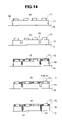
- FIGS. 14( a ) to 14 ( e ) are diagrammatic side views illustrating a method of manufacturing a diode package of the type in which an insulating resin is applied;
- FIG. 15 is a sectional view illustrating a state in which a groove between the semiconductor chips is formed in a V-shape and is filled with an insulating resin
- FIG. 16 is a sectional view illustrating a state in which a groove between the semiconductor chips is formed in a parallel shape and is filled with an insulating resin
- FIG. 17 is a side view schematically illustrating the diode package of the type in which an insulating resin is applied in a groove of the V-shape;
- FIG. 18 is a side view schematically illustrating the diode package of the type in which an insulating resin is applied in a groove which is partially of the V-shape and partially of the parallel shape;
- FIGS. 19( a ) to 19 ( e ) are side views illustrating another method of manufacturing the diode package of the type in which an insulating resin is applied.
- FIG. 20 is a perspective view illustrating the appearance of the diode package of the type in which an insulating resin is applied.
- This embodiment is directed to a diode package, as an example.
- FIG. 3 illustrates the structure of a diode package 50 of the bare chip type.
- This diode package 50 has a so-called lateral structure in which two electrodes, including an anode and a cathode, are formed on the front surface side of the semiconductor chip 10 .
- An electrode 11 is formed on the surface of the semiconductor chip 10 ; an under bump metal member 12 is deposited thereon by, for example, sputtering; and a bump electrode 13 is formed by, for example, plating on the metal member 12 to electrically connect the anode and the cathode to an external substrate.
- a metal layer 14 is plated on the surface of the bump electrode 13 for suppressing such oxidation.
- the bump electrode 13 When the connection to the external substrate is accomplished by soldering (solder junction), the bump electrode 13 is chiefly composed of copper or nickel, and gold is plated as the metal member 14 to suppress the oxidation of the bump electrode 13 .
- the bump electrode 13 has a height of about 20 to 25 ⁇ m. Employment of such a lateral structure makes it possible to lower the height of the package (decrease the height), which, incidentally, enables the thickness of the modules and electronic devices to be decreased.
- FIG. 4 is a graph illustrating a relationship between the height of the bump electrode and the maximum stress occurring in the interface between the semiconductor chip 10 and the bump electrode 13 in the step of reflowing the solder for joining the diode package 50 to the external substrate 16 with the solder.
- FIG. 4 indicates that the maximum stress increases with an increase in the height of the bump electrode 13 , and, with increased stress, cracks tend to occur in the semiconductor chip 10 .
- FIG. 5 is a diagram illustrating, on an enlarged scale, the vicinity of the bump electrode 13 .
- a shearing force F occurs at the end 13 b of the bump electrode 13 due to a difference between the coefficient of expansion ac of the semiconductor chip 10 and the coefficient of expansion ak of the external substrate 16 .
- a bending moment M occurs in the bump electrode 13 due to the shearing force F and the height of the bump electrode 13 , and a stress ⁇ builds up in the interface B between the semiconductor chip 10 and the bump electrode 13 .
- the stress ⁇ increases, cracks tend to develop in the semiconductor chip 10 .
- the bending moment M occurring in the bump electrode 13 must be reduced.
- the height h of the bump electrode 13 must be decreased, and the shearing force F occurring at the end 13 b of the bump electrode must be decreased.
- the external substrate 16 has been plated with solder to a thickness of about 10 ⁇ m.
- the height h of the bump electrode is low, therefore, it becomes difficult to accomplish the connection to the external substrate 16 .
- an increased stress tends to build up in the interface between the semiconductor chip 10 and the bump electrode 13 at the time of mounting the chip 10 on the external substrate. As a result, cracks tend to develop in the semiconductor chip 10 , and this could become the cause of an electrical defect.
- FIG. 6 is a view illustrating a diode package 51 having a structure in which the electrode surface and part of the side surfaces of the semiconductor chip 10 are covered with an insulating resin 15 .
- a polyimide resin is used as the insulating resin 15
- nickel is used as the bump electrode 13
- the polyimide resin has a poor resistance against the migration of copper.
- the polyimide resin must be cured by baking at a high temperature.
- nickel is used as the bump electrode 13
- tin is plated as the metal layer 14 for suppressing the oxidation of the bump electrode 13 .
- the electrode is formed in a region spaced about 5 to 20 ⁇ m away from the surface where the bump electrode 13 is formed. To protect the electrode on the side surface of the semiconductor chip 10 , therefore, a region about 5 to 20 ⁇ m away from the surface of the semiconductor chip may be covered with the insulating resin 15 .
- FIG. 7 is a diagram schematically illustrating the constitution of a diode package 50 of the bare chip type
- FIG. 8 is a diagram schematically illustrating the constitution of a diode package 51 of the type in which an insulating resin has been applied.
- the bump electrode 13 a needs be connected to an external substrate 16 .
- the electrode surface and the side surface of the semiconductor chip 10 are covered with the insulating resin 15 , and, hence, the bump electrode 13 a also is substantially covered with the insulating resin 15 . Accordingly, the portion 14 a for connecting the bump electrode 13 a to the external substrate 16 must be exposed.
- FIG. 9 is a diagram illustrating a state where the diode package 51 , of the type in which an insulating resin is applied, as shown in FIG. 8 , is joined to an external substrate 16 with solder;
- FIG. 10 is a diagram illustrating the constitution of the junction portion on an enlarged scale;
- FIGS. 11( a ) and 11 ( b ) are graphs illustrating a maximum main stress building up in the interface A between the semiconductor chip 10 and the bump electrode 13 at the junction portion, and the cumulative probability of breakdown in the interface A, respectively, in comparison with the results obtained in the case of the diode package 50 of the bare chip type shown in FIG. 7 .
- FIG. 11( a ) illustrates the results of maximum main stress values in comparison
- FIG. 11( b ) illustrates the relationships between the maximum main stress and the cumulative probability of breakdown in comparison.
- the maximum main stress is about 130 MPa and the cumulative probability of breakdown is about 50%.
- the maximum main stress is about 78 MPa and the cumulative probability of breakdown is not larger than 1%.
- FIG. 12 is a diagram schematically illustrating the diode package 50 of the bare chip type or the diode package 51 of the type in which an insulating resin is applied, that is mounted on an external substrate 16 .
- the mounting load P acts on the back surface 10 a of the semiconductor chip 10 , and the bump electrode 13 is pushed onto the external substrate 16 .
- the bump electrode 13 produces a reaction R, as well as being subjected to a compressive stress.
- the semiconductor chip 10 deflects with the bump electrode 13 as a fulcrum, and a tensile stress ⁇ is generated on the electrode surface 10 b of the semiconductor chip 10 .
- FIG. 13 is a graph illustrating, in comparison, the results of tensile stress ⁇ in the case of the diode package 50 of the bare chip type and in the case of the diode package 51 of the type in which an insulating resin is applied.
- the stress ⁇ increases with an increase in the load P that is exerted on the back surface 10 a of the semiconductor chip 10 .
- the result 33 of the diode package 51 of the type in which an insulating resin is applied reveals a stress which is decreased by about 50%. Therefore, it is obvious that a high degree of reliability is maintained if the surfaces of the semiconductor chip 10 are covered with the insulating resin 15 .
- FIGS. 14( a ) to 14 ( e ) are diagrams illustrating the steps of a process for manufacturing the diode package 51 of the type in which an insulating resin is applied.
- a plurality of semiconductor chips 10 are formed on the semiconductor wafer 60 , each having an anode and a cathode on the surface thereof and bump electrodes 13 for electrically connecting the electrodes to the external substrate 16 .
- the surfaces of the semiconductor chips 10 are secured by using a dicing sheet 19 .
- the semiconductor chips 10 are formed in a number of about 40,000 on the 5-inch semiconductor wafer 60 .
- grooves 18 are formed among the semiconductor chips 10 , which grooves are to be filled with an insulating resin 15 .
- the insulating resin 15 to be filled in the grooves 18 serves to insulate and protect the side surfaces of the semiconductor chips 10 and suppresses the peeling of an interface between the insulating resin and the chips during the dicing work.
- the bump electrodes 13 are formed in a region which is deep by about 5 to 20 ⁇ m from the surfaces of the electrodes; and, hence, the range for insulating and protecting the electrodes on the side surfaces of the semiconductor chip 10 may be about 5 to 20 ⁇ m from the chip surface. Therefore, the region of the depth of a minimum of 5 to 20 ⁇ m from the chip surface may be covered with the insulating resin 15 .
- the grooves 18 in the half-dicing have a depth of about 50 ⁇ m and a width of about 40 to 60 ⁇ m. The width varies in relation to the number of semiconductor chips 10 obtained from a piece of semiconductor wafer 60 .
- the surfaces of the bump electrodes 13 and of the semiconductor chips 10 are covered with the insulating resin 15 for protection, causing the grooves 18 formed in the step shown in FIG. 14( b ) to be filled with the insulating resin 15 , and the electrode surfaces of the semiconductor chips 10 are also covered with the insulating resin 15 .
- the insulating resin 15 is dropped on nearly the central portion of the semiconductor wafer 60 .
- the semiconductor wafer 60 is rotated at a relatively low speed so that the grooves 18 formed in the step shown in FIG. 14( b ) are filled with the insulating resin 15 .
- the rotational speed is increased to adjust the thickness of the insulating resin 10 by utilizing centrifugal force.
- a vibration system utilizing vibration of ultrasonic waves or of a low frequency, can be employed, for example.
- the vibration system the insulating resin 15 is dropped on nearly the central portion of the semiconductor wafer 60 , and vibration of ultrasonic waves or of a low frequency is imparted to the semiconductor wafer 60 in order to fill the grooves 18 formed in the step shown in FIG. 14( b ) with the insulating resin 15 and to spread the insulating resin 15 all over the semiconductor wafer 60 .
- the width of the grooves 18 is expanded by imparting a tensile force to the semiconductor wafer 60 in two axial directions intersecting each other; the grooves of the expanded width are then filled with the insulating resin 15 ; and the insulating resin 15 is applied onto the predetermined surface of the semiconductor wafer 60 .
- the semiconductor wafer is pushed onto the curved surface of another member to expand the width of the grooves by bending the wafer surface, and then the grooves of expanded width are filled with the insulating resin 15 , and the insulating resin 15 is applied onto the predetermined surface of the semiconductor wafer 60 .
- the method of expanding the width of the grooves is particularly effective when the grooves 18 formed in the steps shown in FIG. 14( b ) are too small in width and cannot be filled with the insulating resin 15 due the viscosity of the insulating resin 15 .
- the grooves 18 may be formed to have such a shape that the width is broadened at the opening portions of the grooves to facilitate their being favorably filled with the insulating resin 15 .
- FIG. 15 illustrates a state in which the groove is filled with the insulating resin 15 when the opening portions of the grooves are broadened
- FIG. 16 illustrates a state in which the groove is filled with the insulating resin 15 when both side surfaces of the grooves are nearly in parallel and the grooves have nearly an equal width at the opening side and on the bottom side.
- the grooves have a narrow width or when the insulating resin 15 has a high viscosity, in particular, an insufficiently filled state tends to occur, as shown in FIG. 16 .
- this can be improved by forming the grooves in the shape as shown in FIG. 15 .
- the insulating resin 15 is removed from the connection portions 14 a to expose the connection portions 14 a for connecting the bump electrodes 13 to the external substrate 16 .
- the insulating resin 15 which is a photosensitive polyimide, can be removed by the treatment of exposure to light and developing. After the removal, heat treatment is carried out to thermally cure the insulating resin 15 that has been applied to protect the surfaces and the side surfaces of the semiconductor chips 10 .
- the insulating resin 15 which is, for example, a photosensitive polyimide, is left to stand in an environment of about 350° C. for about one hour.
- mutual diffusion may take place depending upon the bump electrodes 13 and the kind of metal plating 14 that is used for preventing oxidation of the bump electrodes 13 .
- the mutual diffusion takes place conspicuously, particularly when the bump electrodes 13 are formed of copper or nickel and when gold is plated, as designated at 14 , for preventing the bump electrodes 13 from being oxidized.
- the mutual diffusion can be prevented by, for example, using tin as the metal plating 14 .
- the diode package 51 is separated into individual pieces by cutting among the semiconductor chips through grooves 20 having a width narrower than that of the grooves 18 that have been filled with the insulating resin 15 in the step shown in FIG. 14( c ), in such a manner that the insulating resin 15 is left on the side surfaces of the semiconductor chips 10 to protect the side surfaces of the semiconductor chips 10 , i.e., in a manner such that the insulating resin 15 in the grooves 18 is left on the side surfaces of the grooves 18 . If the grooves 18 formed in the step shown in FIG.
- the grooves 20 may have a width of about 20 to 30 ⁇ m. If cutting is effected at one time, chipping may occur at portions of the semiconductor chip 10 that are not covered with the insulating resin 15 . It is therefore desired that the cutting is effected through a plurality of notches.
- the insulating resin 15 and the semiconductor chip 10 have different degrees of hardness. Therefore, the insulating resin 15 may be cut at a first step and the semiconductor chip 10 may be cut at a second step.
- FIG. 17 is a side view schematically illustrating the diode package of the type in which an insulating resin is applied, which package is obtained by forming V-shaped grooves, as shown in FIG. 14( b ), applying the insulating resin 15 , as shown in FIG. 14( c ), and cutting the insulating resin in the grooves, as shown in FIG. 14( e ).
- FIG. 18 is a side view schematically illustrating the diode package of the type in which an insulating resin is applied, which package is obtained by forming V-shaped grooves extended by grooves of parallel portions in tha manner shown in FIG. 14( b ), applying the insulating resin 15 in the manner shown in FIG. 14( c ), and cutting the insulating resin in the grooves in the manner shown in FIG. 14( e ).
- FIGS. 19( a ) to 19 ( e ) are diagrams illustrating steps in another manufacturing process according to an embodiment of the present invention.
- This system is a so-called full dicing system.
- This system does not require the step of removing the insulating resin 15 for exposing the connection portions 14 a only for connecting the bump electrodes 13 of FIG. 14( d ) to the external substrate 16 .
- a diode package 55 nearly the whole surfaces of the semiconductor chips 10 (whole surfaces except for the portions connecting the bump electrodes 13 ) are covered with the insulating resin 15 . Therefore, the semiconductor chips 10 exhibit high reliability even when an unexpected load is exerted thereon.
- a plurality of semiconductor chips 10 are formed on the semiconductor wafer 60 , each having an anode and a cathode on the surface thereof and bump electrodes 13 for electrically connecting the electrodes to the external substrate 16 .
- the surfaces (back surfaces) of the semiconductor chips 10 are secured by using a first dicing sheet 21 .
- grooves 23 are formed among the semiconductor chips 10 in order to separate the semiconductor chips 10 .
- the semiconductor chips 10 after being separated, are secured at their back surfaces by the first dicing sheet 21 and are not scattered.
- a second dicing sheet 22 is mounted having an adhering force greater than that of the first dicing sheet 21 which is used for securing the semiconductor wafer 60 , as seen in FIG. 19( b ), and the first dicing sheet 21 is then removed by being peeled off the back surfaces of the semiconductor chips 10 .
- the semiconductor chips 10 are transferred from the surface of the first dicing sheet 21 onto the surface of the second dicing sheet 22 .
- the first dicing sheet 21 needs have an adhering force that does not permit the semiconductor chips 10 to move at the time of forming the grooves 23 .
- the surfaces of the semiconductor chips 10 , the back surfaces thereof (from where the first dicing sheet 21 is peeled off), the side surfaces thereof, and the side surfaces of the bump electrodes 13 are covered with the insulating resin 15 . More specifically, the grooves 23 that are formed as seen in FIG. 19( b ) and the voids 24 , which are formed by the second dicing sheet 22 , by the electrode surfaces of the semiconductor chips 10 and by the bump electrodes 13 , are filled with the insulating resin 15 , and the back surfaces of the semiconductor chips 10 (from where the first dicing sheet 21 is peeled off) are covered with the insulating resin 15 .
- the method of application may be, for example, a vibration system which applies a vibration of ultrasonic waves or of a low frequency to the semiconductor wafer 60 ; or, a dipping system may be employed according to which the insulating resin 15 is introduced into a vessel in advance, and the semiconductor wafer 60 and the second dicing sheet 22 are dipped in the vessel. After the insulating resin 15 is applied, the heat treatment is conducted to thermally cure the insulating resin 15 . At this time, the second dicing sheet 22 is in a state where it secures the semiconductor chips 10 and the bump electrodes 13 , and it must have a resistance against high temperatures.
- the insulating resin 15 after being thermally set is cut in a state where the insulating resin 15 filled in the grooves 23 is partly left on the side surfaces of the grooves 23 to obtain individually divided semiconductor chips 10 .
- the second dicing sheet is removed from the side of the end surfaces of the bump electrodes 13 .
- FIG. 20 is a view illustrating the appearance of the diode package 51 of the type in which an insulating resin is applied.
- the diode package 51 is mounted with its face down on the external substrate 16 .
- the above-described embodiment is capable of providing a small diode package. Since the insulating resin is provided on the electrode surfaces of the semiconductor chips, stress is relaxed in the interface between the semiconductor chips and the bump electrodes, thereby suppressing the occurrence of cracks. It is also possible to decrease the number of manufacturing steps. Since no wire connection is employed, the connection operation is easy and reliability is improved. The insulating resin is applied in the state of the semiconductor wafer, facilitating the application operation and requiring a decreased period of time. The cost can be decreased, as well.
- diode package serving as a semiconductor package having two electrodes, including an anode and a cathode.
- the invention may deal with any semiconductor package in addition to a diode package.
- a small diode package capable of suppressing the occurrence of cracks and exhibiting improved reliability. It is further possible to decrease the number of steps in the manufacturing process, facilitating the operation for connecting the electrodes and for applying the insulating resin. The cost can be decreased as well.
Abstract
Description
Claims (6)
Applications Claiming Priority (2)
| Application Number | Priority Date | Filing Date | Title |
|---|---|---|---|
| JP2001-357775 | 2001-11-22 | ||
| JP2001357775A JP3706573B2 (en) | 2001-11-22 | 2001-11-22 | Semiconductor package and semiconductor package manufacturing method |
Publications (2)
| Publication Number | Publication Date |
|---|---|
| US20030094621A1 US20030094621A1 (en) | 2003-05-22 |
| US7023027B2 true US7023027B2 (en) | 2006-04-04 |
Family
ID=19169067
Family Applications (1)
| Application Number | Title | Priority Date | Filing Date |
|---|---|---|---|
| US10/294,619 Expired - Lifetime US7023027B2 (en) | 2001-11-22 | 2002-11-15 | Diode package having an anode and a cathode formed on one surface of a diode chip |
Country Status (2)
| Country | Link |
|---|---|
| US (1) | US7023027B2 (en) |
| JP (1) | JP3706573B2 (en) |
Cited By (2)
| Publication number | Priority date | Publication date | Assignee | Title |
|---|---|---|---|---|
| US20060154447A1 (en) * | 2005-01-13 | 2006-07-13 | Yoshimasa Kushima | Method for manufacturing semiconductor device |
| US20070096316A1 (en) * | 2005-10-28 | 2007-05-03 | International Rectifier Corporation | Contact pad structure for flip chip semiconductor die |
Families Citing this family (7)
| Publication number | Priority date | Publication date | Assignee | Title |
|---|---|---|---|---|
| JP2004304066A (en) * | 2003-03-31 | 2004-10-28 | Renesas Technology Corp | Method of manufacturing semiconductor device |
| JP2012113919A (en) * | 2010-11-24 | 2012-06-14 | Toshiba Corp | Lighting device |
| JP5517378B1 (en) * | 2013-08-13 | 2014-06-11 | 太陽誘電株式会社 | Circuit module |
| JP6416934B2 (en) * | 2014-12-26 | 2018-10-31 | 株式会社日立製作所 | Semiconductor device, manufacturing method thereof, and semiconductor module |
| CN105489488B (en) * | 2015-11-26 | 2019-04-23 | 泗阳群鑫电子有限公司 | A kind of chip diode is using Jiao Dao as the manufacturing method of ontology |
| JP2019024038A (en) * | 2017-07-24 | 2019-02-14 | 株式会社ディスコ | Wafer processing method |
| US20190206827A1 (en) * | 2017-12-29 | 2019-07-04 | Intel Corporation | Semiconductor package with externally accessible wirebonds |
Citations (11)
| Publication number | Priority date | Publication date | Assignee | Title |
|---|---|---|---|---|
| JPH0562980A (en) | 1991-08-29 | 1993-03-12 | Hitachi Ltd | Semiconductor device and manufacture thereof |
| JPH05326618A (en) | 1992-05-15 | 1993-12-10 | Rohm Co Ltd | Semiconductor device |
| US5393711A (en) * | 1991-10-12 | 1995-02-28 | Robert Bosch Gmbh | Process for manufacturing semiconductor components |
| JPH10162455A (en) | 1996-12-04 | 1998-06-19 | Sony Corp | Magnetic recording and reproducing device and production of drum for magnetic recording and reproducing device |
| JPH11162889A (en) | 1997-11-25 | 1999-06-18 | Sony Corp | Equipment and method for breaking/stretching wafer |
| JPH11214434A (en) | 1998-01-29 | 1999-08-06 | Asahi Kasei Denshi Kk | Semiconductor element and its manufacture |
| US6060768A (en) | 1995-05-09 | 2000-05-09 | Fujitsu Limited | Semiconductor device, method of manufacturing the semiconductor device, and method of manufacturing lead frame |
| JP2001284497A (en) | 2000-04-03 | 2001-10-12 | Fujitsu Ltd | Semiconductor device and manufacturing method therefor, and semiconductor tip and manufacturing method therefor |
| US6607970B1 (en) * | 1999-11-11 | 2003-08-19 | Casio Computer Co., Ltd. | Semiconductor device and method of manufacturing the same |
| US6635962B2 (en) * | 2000-09-12 | 2003-10-21 | Rohm Co. Ltd. | Chip on chip semiconductor device |
| US6780746B2 (en) * | 2000-06-02 | 2004-08-24 | Micron Technology, Inc. | Method for fabricating a chip scale package using wafer level processing and devices resulting therefrom |
-
2001
- 2001-11-22 JP JP2001357775A patent/JP3706573B2/en not_active Expired - Fee Related
-
2002
- 2002-11-15 US US10/294,619 patent/US7023027B2/en not_active Expired - Lifetime
Patent Citations (12)
| Publication number | Priority date | Publication date | Assignee | Title |
|---|---|---|---|---|
| JPH0562980A (en) | 1991-08-29 | 1993-03-12 | Hitachi Ltd | Semiconductor device and manufacture thereof |
| US5393711A (en) * | 1991-10-12 | 1995-02-28 | Robert Bosch Gmbh | Process for manufacturing semiconductor components |
| JPH05326618A (en) | 1992-05-15 | 1993-12-10 | Rohm Co Ltd | Semiconductor device |
| US6060768A (en) | 1995-05-09 | 2000-05-09 | Fujitsu Limited | Semiconductor device, method of manufacturing the semiconductor device, and method of manufacturing lead frame |
| JPH10162455A (en) | 1996-12-04 | 1998-06-19 | Sony Corp | Magnetic recording and reproducing device and production of drum for magnetic recording and reproducing device |
| JPH11162889A (en) | 1997-11-25 | 1999-06-18 | Sony Corp | Equipment and method for breaking/stretching wafer |
| JPH11214434A (en) | 1998-01-29 | 1999-08-06 | Asahi Kasei Denshi Kk | Semiconductor element and its manufacture |
| US6607970B1 (en) * | 1999-11-11 | 2003-08-19 | Casio Computer Co., Ltd. | Semiconductor device and method of manufacturing the same |
| JP2001284497A (en) | 2000-04-03 | 2001-10-12 | Fujitsu Ltd | Semiconductor device and manufacturing method therefor, and semiconductor tip and manufacturing method therefor |
| US6507092B1 (en) | 2000-04-03 | 2003-01-14 | Fujitsu Limited | Semiconductor device having increased reliability and method of producing the same and semiconductor chip suitable for such a semiconductor device and method of producing the same |
| US6780746B2 (en) * | 2000-06-02 | 2004-08-24 | Micron Technology, Inc. | Method for fabricating a chip scale package using wafer level processing and devices resulting therefrom |
| US6635962B2 (en) * | 2000-09-12 | 2003-10-21 | Rohm Co. Ltd. | Chip on chip semiconductor device |
Cited By (4)
| Publication number | Priority date | Publication date | Assignee | Title |
|---|---|---|---|---|
| US20060154447A1 (en) * | 2005-01-13 | 2006-07-13 | Yoshimasa Kushima | Method for manufacturing semiconductor device |
| US7763528B2 (en) * | 2005-01-13 | 2010-07-27 | Oki Semiconductor Co., Ltd. | Method for manufacturing semiconductor device |
| US20070096316A1 (en) * | 2005-10-28 | 2007-05-03 | International Rectifier Corporation | Contact pad structure for flip chip semiconductor die |
| US7821133B2 (en) * | 2005-10-28 | 2010-10-26 | International Rectifier Corporation | Contact pad structure for flip chip semiconductor die |
Also Published As
| Publication number | Publication date |
|---|---|
| JP3706573B2 (en) | 2005-10-12 |
| JP2003158140A (en) | 2003-05-30 |
| US20030094621A1 (en) | 2003-05-22 |
Similar Documents
| Publication | Publication Date | Title |
|---|---|---|
| US6777814B2 (en) | Semiconductor device | |
| JPH10321631A (en) | Semiconductor device and its manufacture | |
| JPS6149432A (en) | Manufacture of semiconductor device | |
| US3387191A (en) | Strain relieving transition member for contacting semiconductor devices | |
| US7023027B2 (en) | Diode package having an anode and a cathode formed on one surface of a diode chip | |
| US5757068A (en) | Carrier film with peripheral slits | |
| JP2000269166A (en) | Manufacture of integrated circuit chip and semiconductor device | |
| JP2838703B2 (en) | Semiconductor package manufacturing method | |
| JPH0158864B2 (en) | ||
| JPH03293740A (en) | Connecting method for semiconductor device | |
| JPS59154054A (en) | Wire and semiconductor device using it | |
| JPH0214779B2 (en) | ||
| EP1018762A2 (en) | Semiconductor device and fabrication method thereof | |
| JP3019065B2 (en) | Semiconductor device connection method | |
| JP3525808B2 (en) | Semiconductor device manufacturing method and semiconductor device | |
| JPS6118157A (en) | Semiconductor device | |
| JP4196954B2 (en) | Semiconductor device | |
| JP3076302B2 (en) | Semiconductor device | |
| JPS62208642A (en) | Mounting of semiconductor device | |
| JPH01135052A (en) | Semiconductor device and manufacture thereof | |
| JPS6335105B2 (en) | ||
| JPS6234143B2 (en) | ||
| JPH08250545A (en) | Semiconductor device and manufacture thereof | |
| JP3077649B2 (en) | Semiconductor device using TCP tape | |
| JPH0158863B2 (en) |
Legal Events
| Date | Code | Title | Description |
|---|---|---|---|
| AS | Assignment |
Owner name: HITACHI, LTD., JAPAN Free format text: ASSIGNMENT OF ASSIGNORS INTEREST;ASSIGNORS:TERAMAE, TOSHIYA;SAEKI, JUNICHI;ICHINOSE, YASUHARU;AND OTHERS;REEL/FRAME:013499/0760;SIGNING DATES FROM 20021101 TO 20021106 |
|
| AS | Assignment |
Owner name: RENESAS TECHNOLOGY CORPORATION, JAPAN Free format text: ASSIGNMENT OF ASSIGNORS INTEREST;ASSIGNOR:HITACHI, LTD.;REEL/FRAME:014569/0585 Effective date: 20030912 |
|
| STCF | Information on status: patent grant |
Free format text: PATENTED CASE |
|
| FEPP | Fee payment procedure |
Free format text: PAYOR NUMBER ASSIGNED (ORIGINAL EVENT CODE: ASPN); ENTITY STATUS OF PATENT OWNER: LARGE ENTITY |
|
| FPAY | Fee payment |
Year of fee payment: 4 |
|
| AS | Assignment |
Owner name: RENESAS ELECTRONICS CORPORATION, JAPAN Free format text: MERGER;ASSIGNOR:RENESAS TECHNOLOGY CORP.;REEL/FRAME:025204/0512 Effective date: 20100401 |
|
| FPAY | Fee payment |
Year of fee payment: 8 |
|
| MAFP | Maintenance fee payment |
Free format text: PAYMENT OF MAINTENANCE FEE, 12TH YEAR, LARGE ENTITY (ORIGINAL EVENT CODE: M1553) Year of fee payment: 12 |
|
| AS | Assignment |
Owner name: RENESAS ELECTRONICS CORPORATION, JAPAN Free format text: CHANGE OF ADDRESS;ASSIGNOR:RENESAS ELECTRONICS CORPORATION;REEL/FRAME:044928/0001 Effective date: 20150806 |