US7022594B2 - Manufacturing method which prevents abnormal gate oxidation - Google Patents
Manufacturing method which prevents abnormal gate oxidation Download PDFInfo
- Publication number
- US7022594B2 US7022594B2 US10/737,821 US73782103A US7022594B2 US 7022594 B2 US7022594 B2 US 7022594B2 US 73782103 A US73782103 A US 73782103A US 7022594 B2 US7022594 B2 US 7022594B2
- Authority
- US
- United States
- Prior art keywords
- film
- forming
- gate electrode
- impurity
- silicon
- Prior art date
- Legal status (The legal status is an assumption and is not a legal conclusion. Google has not performed a legal analysis and makes no representation as to the accuracy of the status listed.)
- Expired - Fee Related
Links
- 238000004519 manufacturing process Methods 0.000 title claims abstract description 32
- 238000007254 oxidation reaction Methods 0.000 title claims abstract description 19
- 230000003647 oxidation Effects 0.000 title claims abstract description 17
- 230000002159 abnormal effect Effects 0.000 title abstract description 5
- 229910021420 polycrystalline silicon Inorganic materials 0.000 claims abstract description 116
- 229920005591 polysilicon Polymers 0.000 claims abstract description 116
- 239000012535 impurity Substances 0.000 claims abstract description 112
- 238000000034 method Methods 0.000 claims abstract description 94
- 150000004767 nitrides Chemical class 0.000 claims abstract description 54
- 238000009792 diffusion process Methods 0.000 claims abstract description 51
- 239000003870 refractory metal Substances 0.000 claims abstract description 42
- XUIMIQQOPSSXEZ-UHFFFAOYSA-N Silicon Chemical compound [Si] XUIMIQQOPSSXEZ-UHFFFAOYSA-N 0.000 claims abstract description 40
- 229910052710 silicon Inorganic materials 0.000 claims abstract description 40
- 239000010703 silicon Substances 0.000 claims abstract description 40
- 229910021332 silicide Inorganic materials 0.000 claims abstract description 32
- FVBUAEGBCNSCDD-UHFFFAOYSA-N silicide(4-) Chemical compound [Si-4] FVBUAEGBCNSCDD-UHFFFAOYSA-N 0.000 claims abstract description 32
- 239000000758 substrate Substances 0.000 claims abstract description 31
- 239000004065 semiconductor Substances 0.000 claims abstract description 22
- 238000000059 patterning Methods 0.000 claims abstract description 6
- 125000006850 spacer group Chemical group 0.000 claims description 25
- 229910021417 amorphous silicon Inorganic materials 0.000 claims description 19
- 230000001590 oxidative effect Effects 0.000 claims description 4
- 206010010144 Completed suicide Diseases 0.000 claims 2
- WQJQOUPTWCFRMM-UHFFFAOYSA-N tungsten disilicide Chemical compound [Si]#[W]#[Si] WQJQOUPTWCFRMM-UHFFFAOYSA-N 0.000 description 39
- 238000004518 low pressure chemical vapour deposition Methods 0.000 description 26
- 238000005530 etching Methods 0.000 description 23
- 229910021342 tungsten silicide Inorganic materials 0.000 description 20
- 238000005468 ion implantation Methods 0.000 description 14
- 238000000206 photolithography Methods 0.000 description 11
- 229910021341 titanium silicide Inorganic materials 0.000 description 11
- 238000004544 sputter deposition Methods 0.000 description 10
- 230000015572 biosynthetic process Effects 0.000 description 8
- 229910044991 metal oxide Inorganic materials 0.000 description 8
- 150000004706 metal oxides Chemical class 0.000 description 8
- 239000007789 gas Substances 0.000 description 7
- 238000010438 heat treatment Methods 0.000 description 7
- WFKWXMTUELFFGS-UHFFFAOYSA-N tungsten Chemical compound [W] WFKWXMTUELFFGS-UHFFFAOYSA-N 0.000 description 7
- 229910052721 tungsten Inorganic materials 0.000 description 7
- 239000010937 tungsten Substances 0.000 description 7
- 238000009413 insulation Methods 0.000 description 6
- 239000012298 atmosphere Substances 0.000 description 5
- 238000010586 diagram Methods 0.000 description 5
- XKRFYHLGVUSROY-UHFFFAOYSA-N Argon Chemical compound [Ar] XKRFYHLGVUSROY-UHFFFAOYSA-N 0.000 description 4
- OAICVXFJPJFONN-UHFFFAOYSA-N Phosphorus Chemical compound [P] OAICVXFJPJFONN-UHFFFAOYSA-N 0.000 description 4
- 238000010924 continuous production Methods 0.000 description 4
- 150000002500 ions Chemical class 0.000 description 4
- 229910052751 metal Inorganic materials 0.000 description 4
- 239000002184 metal Substances 0.000 description 4
- 229910052698 phosphorus Inorganic materials 0.000 description 4
- 239000011574 phosphorus Substances 0.000 description 4
- 239000003990 capacitor Substances 0.000 description 3
- ZOXJGFHDIHLPTG-UHFFFAOYSA-N Boron Chemical compound [B] ZOXJGFHDIHLPTG-UHFFFAOYSA-N 0.000 description 2
- XYFCBTPGUUZFHI-UHFFFAOYSA-N Phosphine Chemical compound P XYFCBTPGUUZFHI-UHFFFAOYSA-N 0.000 description 2
- 229910052786 argon Inorganic materials 0.000 description 2
- 229910052796 boron Inorganic materials 0.000 description 2
- 238000002425 crystallisation Methods 0.000 description 2
- 230000008025 crystallization Effects 0.000 description 2
- 230000009977 dual effect Effects 0.000 description 2
- 238000000926 separation method Methods 0.000 description 2
- BLRPTPMANUNPDV-UHFFFAOYSA-N Silane Chemical compound [SiH4] BLRPTPMANUNPDV-UHFFFAOYSA-N 0.000 description 1
- 229910052782 aluminium Inorganic materials 0.000 description 1
- XAGFODPZIPBFFR-UHFFFAOYSA-N aluminium Chemical compound [Al] XAGFODPZIPBFFR-UHFFFAOYSA-N 0.000 description 1
- 229910052785 arsenic Inorganic materials 0.000 description 1
- RQNWIZPPADIBDY-UHFFFAOYSA-N arsenic atom Chemical compound [As] RQNWIZPPADIBDY-UHFFFAOYSA-N 0.000 description 1
- 238000005229 chemical vapour deposition Methods 0.000 description 1
- 239000004020 conductor Substances 0.000 description 1
- 238000007796 conventional method Methods 0.000 description 1
- 238000002513 implantation Methods 0.000 description 1
- 238000002844 melting Methods 0.000 description 1
- 239000012299 nitrogen atmosphere Substances 0.000 description 1
- 229910000073 phosphorus hydride Inorganic materials 0.000 description 1
- 229920001296 polysiloxane Polymers 0.000 description 1
- 238000005204 segregation Methods 0.000 description 1
- 229910000077 silane Inorganic materials 0.000 description 1
- 230000001629 suppression Effects 0.000 description 1
Images


Classifications
-
- H—ELECTRICITY
- H01—ELECTRIC ELEMENTS
- H01L—SEMICONDUCTOR DEVICES NOT COVERED BY CLASS H10
- H01L21/00—Processes or apparatus adapted for the manufacture or treatment of semiconductor or solid state devices or of parts thereof
- H01L21/02—Manufacture or treatment of semiconductor devices or of parts thereof
- H01L21/04—Manufacture or treatment of semiconductor devices or of parts thereof the devices having at least one potential-jump barrier or surface barrier, e.g. PN junction, depletion layer or carrier concentration layer
- H01L21/18—Manufacture or treatment of semiconductor devices or of parts thereof the devices having at least one potential-jump barrier or surface barrier, e.g. PN junction, depletion layer or carrier concentration layer the devices having semiconductor bodies comprising elements of Group IV of the Periodic System or AIIIBV compounds with or without impurities, e.g. doping materials
- H01L21/28—Manufacture of electrodes on semiconductor bodies using processes or apparatus not provided for in groups H01L21/20 - H01L21/268
- H01L21/28008—Making conductor-insulator-semiconductor electrodes
- H01L21/28017—Making conductor-insulator-semiconductor electrodes the insulator being formed after the semiconductor body, the semiconductor being silicon
- H01L21/28247—Making conductor-insulator-semiconductor electrodes the insulator being formed after the semiconductor body, the semiconductor being silicon passivation or protection of the electrode, e.g. using re-oxidation
-
- H—ELECTRICITY
- H01—ELECTRIC ELEMENTS
- H01L—SEMICONDUCTOR DEVICES NOT COVERED BY CLASS H10
- H01L21/00—Processes or apparatus adapted for the manufacture or treatment of semiconductor or solid state devices or of parts thereof
- H01L21/02—Manufacture or treatment of semiconductor devices or of parts thereof
- H01L21/04—Manufacture or treatment of semiconductor devices or of parts thereof the devices having at least one potential-jump barrier or surface barrier, e.g. PN junction, depletion layer or carrier concentration layer
- H01L21/18—Manufacture or treatment of semiconductor devices or of parts thereof the devices having at least one potential-jump barrier or surface barrier, e.g. PN junction, depletion layer or carrier concentration layer the devices having semiconductor bodies comprising elements of Group IV of the Periodic System or AIIIBV compounds with or without impurities, e.g. doping materials
- H01L21/28—Manufacture of electrodes on semiconductor bodies using processes or apparatus not provided for in groups H01L21/20 - H01L21/268
- H01L21/28008—Making conductor-insulator-semiconductor electrodes
- H01L21/28017—Making conductor-insulator-semiconductor electrodes the insulator being formed after the semiconductor body, the semiconductor being silicon
- H01L21/28026—Making conductor-insulator-semiconductor electrodes the insulator being formed after the semiconductor body, the semiconductor being silicon characterised by the conductor
- H01L21/28035—Making conductor-insulator-semiconductor electrodes the insulator being formed after the semiconductor body, the semiconductor being silicon characterised by the conductor the final conductor layer next to the insulator being silicon, e.g. polysilicon, with or without impurities
- H01L21/28044—Making conductor-insulator-semiconductor electrodes the insulator being formed after the semiconductor body, the semiconductor being silicon characterised by the conductor the final conductor layer next to the insulator being silicon, e.g. polysilicon, with or without impurities the conductor comprising at least another non-silicon conductive layer
- H01L21/28061—Making conductor-insulator-semiconductor electrodes the insulator being formed after the semiconductor body, the semiconductor being silicon characterised by the conductor the final conductor layer next to the insulator being silicon, e.g. polysilicon, with or without impurities the conductor comprising at least another non-silicon conductive layer the conductor comprising a metal or metal silicide formed by deposition, e.g. sputter deposition, i.e. without a silicidation reaction
-
- H—ELECTRICITY
- H01—ELECTRIC ELEMENTS
- H01L—SEMICONDUCTOR DEVICES NOT COVERED BY CLASS H10
- H01L29/00—Semiconductor devices adapted for rectifying, amplifying, oscillating or switching, or capacitors or resistors with at least one potential-jump barrier or surface barrier, e.g. PN junction depletion layer or carrier concentration layer; Details of semiconductor bodies or of electrodes thereof ; Multistep manufacturing processes therefor
- H01L29/40—Electrodes ; Multistep manufacturing processes therefor
- H01L29/43—Electrodes ; Multistep manufacturing processes therefor characterised by the materials of which they are formed
- H01L29/49—Metal-insulator-semiconductor electrodes, e.g. gates of MOSFET
- H01L29/4916—Metal-insulator-semiconductor electrodes, e.g. gates of MOSFET the conductor material next to the insulator being a silicon layer, e.g. polysilicon doped with boron, phosphorus or nitrogen
- H01L29/4925—Metal-insulator-semiconductor electrodes, e.g. gates of MOSFET the conductor material next to the insulator being a silicon layer, e.g. polysilicon doped with boron, phosphorus or nitrogen with a multiple layer structure, e.g. several silicon layers with different crystal structure or grain arrangement
- H01L29/4941—Metal-insulator-semiconductor electrodes, e.g. gates of MOSFET the conductor material next to the insulator being a silicon layer, e.g. polysilicon doped with boron, phosphorus or nitrogen with a multiple layer structure, e.g. several silicon layers with different crystal structure or grain arrangement with a barrier layer between the silicon and the metal or metal silicide upper layer, e.g. Silicide/TiN/Polysilicon
-
- H—ELECTRICITY
- H01—ELECTRIC ELEMENTS
- H01L—SEMICONDUCTOR DEVICES NOT COVERED BY CLASS H10
- H01L29/00—Semiconductor devices adapted for rectifying, amplifying, oscillating or switching, or capacitors or resistors with at least one potential-jump barrier or surface barrier, e.g. PN junction depletion layer or carrier concentration layer; Details of semiconductor bodies or of electrodes thereof ; Multistep manufacturing processes therefor
- H01L29/66—Types of semiconductor device ; Multistep manufacturing processes therefor
- H01L29/66007—Multistep manufacturing processes
- H01L29/66075—Multistep manufacturing processes of devices having semiconductor bodies comprising group 14 or group 13/15 materials
- H01L29/66227—Multistep manufacturing processes of devices having semiconductor bodies comprising group 14 or group 13/15 materials the devices being controllable only by the electric current supplied or the electric potential applied, to an electrode which does not carry the current to be rectified, amplified or switched, e.g. three-terminal devices
- H01L29/66409—Unipolar field-effect transistors
- H01L29/66477—Unipolar field-effect transistors with an insulated gate, i.e. MISFET
- H01L29/6656—Unipolar field-effect transistors with an insulated gate, i.e. MISFET using multiple spacer layers, e.g. multiple sidewall spacers
-
- H—ELECTRICITY
- H01—ELECTRIC ELEMENTS
- H01L—SEMICONDUCTOR DEVICES NOT COVERED BY CLASS H10
- H01L29/00—Semiconductor devices adapted for rectifying, amplifying, oscillating or switching, or capacitors or resistors with at least one potential-jump barrier or surface barrier, e.g. PN junction depletion layer or carrier concentration layer; Details of semiconductor bodies or of electrodes thereof ; Multistep manufacturing processes therefor
- H01L29/66—Types of semiconductor device ; Multistep manufacturing processes therefor
- H01L29/66007—Multistep manufacturing processes
- H01L29/66075—Multistep manufacturing processes of devices having semiconductor bodies comprising group 14 or group 13/15 materials
- H01L29/66227—Multistep manufacturing processes of devices having semiconductor bodies comprising group 14 or group 13/15 materials the devices being controllable only by the electric current supplied or the electric potential applied, to an electrode which does not carry the current to be rectified, amplified or switched, e.g. three-terminal devices
- H01L29/66409—Unipolar field-effect transistors
- H01L29/66477—Unipolar field-effect transistors with an insulated gate, i.e. MISFET
- H01L29/66568—Lateral single gate silicon transistors
- H01L29/66575—Lateral single gate silicon transistors where the source and drain or source and drain extensions are self-aligned to the sides of the gate
- H01L29/6659—Lateral single gate silicon transistors where the source and drain or source and drain extensions are self-aligned to the sides of the gate with both lightly doped source and drain extensions and source and drain self-aligned to the sides of the gate, e.g. lightly doped drain [LDD] MOSFET, double diffused drain [DDD] MOSFET
Definitions
- the present invention relates to a polycide gate electrode in a semiconductor device, and more particularly to a gate electrode structure for a MOS (Metal Oxide Semiconductor) type transistor having a dial gate structure for use in N-type and P-type polycide gate electrodes, and a manufacturing method thereof.
- MOS Metal Oxide Semiconductor
- a P-type well 12 is formed on a silicon substrate 10 as a semiconductor substrate, and a field oxide film 14 a for separating an device is formed.
- a gate oxide film 14 b having a thickness of 10 nm is formed on a transistor forming portion.
- a polysilicon film is then formed on the entire surface so as to have a thickness of 10 nm by the LP-CVD (Low Pressure—Chemical Vapor Deposition) method.
- the polysilicon film in a P-type MOS transistor forming region is masked with a resist in a photolithography process, and implantation of the N-type impurity ion (phosphorus, arsenic and others) is carried out.
- the impurity diffusion is performed by the heat treatment after removing the resist so that a polysilicon film 16 (which will be simply referred to as an impurity diffused polysilicon film hereinafter) in which the N-type impurity is diffused is formed.
- a titanium silicide film (TiSi 2 ) 18 having a thickness of 5 nm is formed on the polysilicon film having the impurity diffused polysilicon film as an impurity diffusion preventing film.
- a tungsten silicide film (WSix) 20 is thereafter formed on the titanium silicide film as a refractory metal silicide film so as to have a thickness of 100 nm.
- a nitride film 22 having a thickness of 100 nm is formed on the tungsten film for insulation. This state is shown in FIG. 7( a ).
- a gate electrode pattern is formed by the photolithography and etching processes.
- the P-type MOS transistor forming region is masked with the resist in the photolithography process, and impurity ion implantation is carried out in order to form an N-diffusion layer 24 having an LDD (lightly Doped Drain) structure. This state is shown in FIG. 7( b ).
- the oxidation process is effected with respect to the silicon substrate including the gate electrode pattern so that the oxide film 50 is formed on the side surface of the gate electrode.
- the nitride film having a thickness of 300 to 400 nm is formed on the gate electrode which is exposed together with the oxide film on the gate electrode side surface.
- the nitride film is subjected to the anisotropic etching to form a second spacer 28 on the side surface of the gate electrode.
- the gate electrode and the exposed gate oxide film in the P-type MOS transistor forming region are masked with the resist by the photolithography process, and the impurity ion plantation for forming the N + diffusion layer 30 for the source and the drain is carried out. This state is shown in FIG. 7( c ).
- An insulating film 52 such as the oxide film having a thickness of 400 to 800 nm is formed on the gate electrode, the exposed gate electrode oxide film and the field oxide film for insulation by the CVD method, and the surface of this insulating film 52 is smoothed. Thereafter, an opening portion 33 for a contact is formed by the photolithography and etching processes. This state is shown in FIG. 7( d ).
- a metal 55 such as tungsten is embedded in the contact opening portion 33 .
- a metal film such as aluminum is formed on the insulating film 52 including the metal 55 so as to have a thickness of 500 to 800 nm.
- a wiring 54 is formed by the photolithography and etching processes. This state is shown in FIG. 7( e ).
- FIG. 8( a ) is a schematic plan view showing a TEG pattern after forming the contact opening portion.
- FIG. 8( b ) is a view showing the cross-sectional shape taken along the 8 ( b )— 8 ( b ) line in FIG. 8A .
- the cross-sectional shape shown in FIG. 7( d ) corresponds to the line 7 ( d )— 7 ( d ) in FIG. 8( a ). Since the dual gate structure is provided, the N-type well 13 is formed on the side of the PMOS transistor as shown in FIGS. 8( a ) and 8 ( b ) which are schematic plan view and a cross sectional view, respectively.
- the following process is carried out with respect to the gate electrode polysilicon on the PMOS transistor side as similar to the method for forming the impurity diffusion polysilicon on the N-type MOS transistor side.
- the polysilicon in the N-type MOS transistor forming region is masked with the resist in the photolithography process and the P-type impurity ion (which is mainly boron) is imoplanted in the polysilicon film on the PMOS transistor side.
- the P-type impurity is diffused by the heat treatment after removing the resist so that the P-type impurity diffused polysilicon film 17 is formed. Therefore, as shown in the cross-sectional view of FIG. 8( b ), the N-type impurity diffused region and the P-type impuriyt diffused region exist in the polysilicon film formed in one step.
- the N-type diffused region and the P-type diffused region exist in the polysilicon film formed in one step.
- the impurity diffusion preventing film is formed for preventing the mutual diffusion of the N-type impurity and the P-type impurity.
- the silicon is not supplied from the impurity doped polysilicon.
- abnormal oxidization such as that a refractory metal oxide film (W 2 O 3 ) which is an oxide of tungsten is formed. This abnormal oxide portion results in a pattern failure.
- the gate electrode structure for the MOS-type transistor according to the present invention is constituted by: a gate electrode in which an impurity diffused polysilicon film, an impurity diffusion preventing film, a silicon-based film, a refractory metal silicide film and a nitride film are superimposed in the mentioned order; and an oxide film for covering the side surfaces of the impurity diffused polysilicon film, the impurity diffusion preventing film, the silicone-based film and the refractory metal silicide film.
- the silicon-based film may be a polysilicon film or an amorphous silicon film.
- the gate electrode structure according to the present invention can be obtained by the following manufacturing method comprising: a step for forming an insulating film on a semiconductor substrate surface; a step for forming an impurity diffused polysilicon film on the insulating film; a step for forming an impurity diffusion preventing film on the impurity diffused polysilicon film; a step for forming a silicon-based film on the impurity diffusion preventing film; a step for forming a refractory metal silicide film on the silicon-based film; a step for forming a nitride film on the refractory metal silicide film; a step for patterning the impurity diffused polysilicon film, the impurity diffusion preventing film, the silicon-based film; the high-melting point metal silicide film and the nitride film on the gate electrode; and a step for performing an oxidation process.
- FIGS. 1 ( a )– 1 ( d ) are flow diagrams of cross-sectional forms showing a gate electrode manufacturing method according to a first embodiment of the present invention
- FIGS. 2( a )– 2 ( d ) are flow diagrams of cross-sectional forms showing a gate electrode manufacturing method according to a second embodiment of the present invention
- FIG. 3 is a cross-sectional form view of a gate electrode structure according to a third embodiment of the present invention.
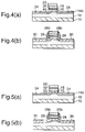
- FIGS. 4( a ) and 4 ( b ) are flow diagrams of cross-sectional forms showing a gate electrode manufacturing method according to a fourth embodiment of the present invention.
- FIGS. 5( a ) and 5 ( b ) are flow diagrams of cross-sectional forms showing a gate electrode manufacturing method according to a fifth embodiment of the present invention.
- FIGS. 6( a )– 6 ( e ) are cross-sectional form views of a gate electrode according to another manufacturing method in the first to fifth embodiments of the present invention.
- FIGS. 7( a )– 7 ( e ) are flow diagrams of cross-sectional forms showing a gate electrode manufacturing method according to a prior art.
- FIGS. 8( a ) and 8 ( b ) are a plan pattern view and a cross-sectional form view of TEGs of N-type MOS and P-type MOS transistors manufactured according to the prior art.
- a silicon substrate is used as a semiconductor substrate.
- description will be given as to an N-type MOS transistor side. If the conductor type of the P-type MOS transistor is reversed, its structure and manufacturing method become similar to those of the N-type MOS transistor, and hence their explanation will be omitted. Further, description as to the device separation region of the field oxide film shown in FIG. 7 will be also omitted.
- a P-type well 12 is formed on a silicon substrate 10 as a semiconductor substrate.
- a gate oxide film 14 b having a thickness of 10 nm is formed as an insulating film on a transistor forming portion on the surface of the P-type well 12 which is the semiconductor substrate.
- a polysilicon film having a thickness of 100 nm is formed on the gate oxide film 14 b by the LP-CVD method.
- the N-type impurity ion implantation is performed with respect to the polysilicon film.
- the N-type impurity diffusion is carried out to the polysilicon film by the heat treatment, and an impurity diffused polysilicon film 16 is formed.
- a titanium silicide film 18 as an impurity diffusion preventing film is then formed on the impurity diffused polysilicon film 16 so as to have a thickness of 5 nm. Thereafter, a tungsten silicide film 20 having a thickness of 100 nm as refractory metal silicide is formed on the titanium silicide film 18 . Moreover, a nitride film having a thickness of 100 nm is formed on the tungsten silicide film 20 for insulation.
- the gate electrode is patterned by the photolithography and etching processes. Further, the impurity ion implantation is carried out with respect to the surface of the P-type well 12 through the exposed gate oxide film in order to form an N ⁇ diffusion layer 24 having the LDD structure. This state is shown in FIG. 1( a ).
- a polysilicon film 26 having a thickness of 10 to 20 nm is formed as a silicon-based film on at least the top surface and the side surfaces of the gate electrode ( FIG. 1( b )).
- Anisotropic etching is performed to the polysilicon film 26 , and a first spacer 26 a consisting of the polysilicon film is formed on the side surfaces of the gate electrode. This state is shown in FIG. 1( c ).
- the first spacer of the polysilicon film becomes an oxide film 26 b by the subsequent oxidation process.
- a nitride film having a thickness of 300 to 400 nm is then formed by the LP-CVD method so as to cover the gate electrode including the oxide film 26 b .
- the anisotropic etching is carried out with respect to the nitride film so that a second spacer 28 consisting of the nitride film is formed on the side surfaces of the gate electrode through the oxide film 26 b .
- the impurity ion implantation is effected with respect to the surface of the P-type well 12 through the exposed gate oxide film in order to form an N + diffusion layer 30 for the source and the drain. This state is shown in FIG. 1( d ). Thereafter, a transistor TEG is formed as similar to the prior art.
- the silicon of the first spacer 26 a is consumed to form the oxide film 26 b . Therefore, the refractory metal oxide film is hardly formed as compared with the prior art. Further, in this case, since the oxide film 26 b is also formed on the side surfaces of the nitride film 22 , the side wall of the gate electrode has no step portion formed thereon and is substantially uniformly formed, which is preferable.
- the first spacer 26 a is formed by the polysilicon film as the silicon-based film, an amorphous silicon film may be likewise used.
- a P-type well 12 is formed on a silicon substrate 10 as a semiconductor substrate.
- a gate oxide film 14 b having a thickness of 10 nm is formed as an insulating film on a transistor forming portion on the surface of the P-type well 12 which is the semiconductor substrate.
- a polysilicon film is then formed on the gate oxide film 14 b by the LP-CVD method so as to have a thickness of 10 nm.
- N-type impurity ion implantation is carried out with respect to the polysilicon film. The N-type impurity is diffused in the polysilicon film by the heat treatment so that an impurity diffused polysilicon film 16 is formed.
- a titanium silicide film 18 as an impurity diffusion preventing film is then-formed on the impurity diffused polysilicon film 16 so as to have a thickness of 5 nm. Thereafter, a tungsten silicide film 20 as refractory metal silicide is formed on the titanium silicide film 18 so as to have a thickness of 10 nm. A nitride film 22 having a thickness of 100 nm is formed on the tungsten silicide film 20 for insulation. A resist film applied onto the nitride film 22 is formed to the pattern of the gate electrode by the photolithography process.
- Etching is effected from the upper-most nitride film 22 to the titanium silicide film 18 , and the resist film is then removed to form a gate electrode pattern. This is determined as a first gate electrode. This state is shown in FIG. 2( a ).
- a nitride film 36 is formed on at least the top surface and the side surfaces of the first gate electrode by the LP-CVD method so as to have a thickness of 10 to 20 nm. ( FIG. 2( b ).
- anisotropic etching is carried out with respect to this nitride film 36 in such a manner that the nitride film remains on the side surfaces of the first gate.
- the nitride film remaining on the side surface of the first gate electrode by the anisotropic etching is determined as a first spacer 36 a .
- the impurity diffused polysilicon film 16 is then subjected to the anisotropic etching with the nitride film 22 and the first spacer 36 a as a mask.
- the impurity diffused polysilicon 16 a patterned by the anisotropic etching and the first gate electrode pattern having the first spacer 36 a provided on the side surfaces thereof form an electrode.
- the electrode constituted by the impurity diffused polysilicon 16 a , the first spacer 36 a and the first gate electrode is determined as a second gate electrode. Further, impurity ion implantation is carried out to the surface of the P-type well 12 through the exposed gate oxide film in order to form an N ⁇ diffusion layer 24 havin an LLD structure. This state is shown in FIG. 2( c ).
- the subsequent oxidation process forms an oxide film 26 b on the side surfaces of the impurity diffused polysilicon 16 .
- a nitride film having a thickness of 300 to 400 nm is formed on the exposed gate oxide film including the second gate electrode and the oxide film 26 b by the LP-CVD method.
- the anisotropic etching is then performed with respect to the nitride film in such a manner that the nitride film remains on the side surfaces of the second gate electrode.
- the nitride film remaining on the side surface of the second gate electrode by the anisotropic etching is determined as a second spacer 28 .
- the impurity ion implantation is carried out to the surface of the P-type well through the exposed gate oxide film in order to form an N + diffusion layer 30 for the source and the drain. This state is shown in FIG. 2( d ). Thereafter, the operation similar to those in the prior art explained above is carried out to form a transistor TEG.
- the refractory metal oxide film is rarely formed when performing the oxidation process for forming the oxide film 26 b.
- a method for manufacturing a gate electrode in a third embodiment according to the present invention will now be described hereunder with reference to FIG. 3 .
- a P-type well 12 is formed on a silicon substrate 10 as a semiconductor substrate.
- a gate oxide film 14 b having a thickness of 10 nm is formed as an insulating film on a transistor forming portion on the surface of the P-type well 12 which is the semiconductor substrate.
- a polysilicon film having a thickness of 100 nm is then formed on the gate oxide film 14 b by the LP-CVD method.
- N-type impurity ion implantation is carried out with respect to the polysilicon film. The N-type impurity is diffused in the polysilicon film by the heat treatment so that an impurity diffused polysilicon film 16 is formed.
- a nitride film 38 is formed as an impurity diffusion preventing film on the impurity diffused polysilicon film so as to have a thickness of 5 nm by the LP-CVD method.
- a tungsten silicide film 20 is then formed as a refractory metal silicide film on the nitride film 38 so as to have a thickness of 100 nm.
- the subsequent steps are carried out as similar to the second embodiment to form a gate electrode ( FIG. 3 ). Further, a transistor TEG is formed.
- the base film is covered with the nitride film 38 and the top layer and the side surface are also covered with the nitride film in the tungsten silicide 20 which is a refractory metal silicide film. Therefore, a refractory metal oxide film is hardly formed in the oxidation process for forming the oxide film 26 b.
- a method for forming the nitride film 38 as the impurity diffusion preventing film there are following two methods besides the above LP-CVD method.
- One is a method for forming the nitride film on the surface of the base polysilicon film by carrying out RTP (Rapid Thermal Process) in NH 3 gas atmosphere at a temperature of 800 to 900° C.
- the other one is a method for forming the base polysilicon film by the LP-CVD method and thereafter forming the nitride film on the surface of the polysilicon film by performing the NH 3 gas atmosphere process at a temperature of 800 to 900° C. in a furnace in which the polysilicon has been formed.
- the first method since the process for each silicon substrate is allowed, a film thickness can be changed in accordance with each substrate. Further, when a number of substrates to be processed is small in the first method, the total processing time is shorter than that of the ordinary batch processing.
- the second method since the polysilicon formation and the nitride film formation are continuously carried out in the same apparatus, there occurs no problem of the organic pollution in a clean room.
- a method for manufacturing a gate electrode in a fourth embodiment according to the present invention will now be described hereunder with reference to FIG. 4 .
- a P-type well 12 is formed on a silicon substrate 10 as a semiconductor substrate.
- a gate oxide film 14 b having a thickness of 10 nm is formed as an insulating film on a transistor forming portion on the surface of the P-type well 12 which is the semiconductor substrate.
- a polysilicon film having a thickness of 100 nm is then formed on the gate oxide film 14 b by the LP-CVD method.
- N-type impurity ion implantation is carried out with respect to this polysilicon film. The N-type impurity is diffused in the polysilicon film by the heat treatment so that an impurity diffused polysilicon film 16 is formed.
- a titanium silicide film 18 is formed on this impurity diffused polysilicon film 16 as an impurity diffusion preventing film so as to have a thickness of 5 nm.
- a polysilicon film 40 as a silicon-based film is formed on the titanium silicide film 18 so as to have a thickness of 5 to 20 nm by the LP-CVD method.
- a tungsten silicide film 20 having a thickness of 100 nm is formed on this polysilicon film 40 as a refractory metal silicide.
- a nitride film 22 having a thickness of 100 nm is formed on the tungsten silicide film. 20 for insulation.
- a gate electrode is patterned by the photolithography and etching processes. Further, impurity ion implantation is carried out with respect to the surface of the P-type well 12 through the exposed gate oxide film in order to form an N ⁇ diffusion layer 24 having an LDD structure. This state is shown in FIG. 4( a )
- the oxidation process is then performed so that an oxide film 26 b is formed on the side surface of the gate electrode.
- a nitride film having a thickness of 300 to 400 nm is formed on the exposed gate oxide film including the oxide film 26 b and the gate electrode by the LP-CVD method.
- Anisotropic etching is then effected to this nitride film in such a manner that the nitride film remains on the side surfaces of the gate electrode including the oxide film 26 .
- the nitride film remaining on the side surface of the gate electrode by this anisotropic etching is determined as a second spacer 28 .
- Impurity ion implantation is carried out with respect to the surface of the P-type well 12 through the exposed gate oxide film in order to form an N + diffusion layer 30 for the source and the drain. This state is shown in FIG. 4( b ).
- the subsequent processes are performed as similar to those in the prior art described above so that a transistor TEG is formed.
- the base film for the tungsten silicide film 20 which is the refractory metal silicide film is the polysilicon film 40 , the refractory metal oxide film is not formed but the oxide film is formed by the silicon supplied from the polysilicon film 40 in the oxidative process for forming the oxide film 26 b.
- the polysilicon film 40 which is the base film for the tungsten silicide film 20 which is the refractory metal silicide film may be an amorphous silicon film obtained by the LP-CVD method.
- an amorphous silicon film can be formed on the impurity diffusion preventing film 18 in the continuous process in this sputtering apparatus by the sputtering method.
- the process is enabled at a temperature lower than a temperature for forming the polysilicon film, e.g., 500° C.
- a temperature for forming the polysilicon film e.g. 500° C.
- a natural oxide film and the like on the surface of the impurity diffusion preventing film 18 can be removed by the etching using argon gas before forming the amorphous silicon film in the sputtering apparatus.
- a method for manufacturing a gate electrode in a fifth embodiment according to the present invention will now be described hereunder with reference to FIG. 5 .
- a P-type well 12 is formed on a silicon substrate 10 as a semiconductor substrate.
- a gate oxide film 14 b having a thickness of 10 nm is formed as an insulating film on a transistor forming portion on the surface of the P-type well 12 which is the semiconductor substrate.
- a polysilicon film having a thickness of 100 nm is formed on the gate oxide film 14 b by the LP-CVD method.
- N-type impurity ion implantation is carried out with respect to the polysilicon film. The N-type impurity is diffused in the polysilicon film by the heat treatment so that an impurity diffused polysilicon film 16 is formed.
- a titanium silicide film 18 having a thickness of 5 nm is then formed as an impurity diffusion preventing film on the impurity diffused polysilicon film 16 .
- a tungsten silicide film 20 is formed as a refractory metal silicide on the titanium silicide film 18 so as to have a thickness of 100 nm.
- a polysilicon film 42 as a silicon-based film is formed on the tungsten silicide film 20 so as to have a thickness of 5 to 20 nm by the LP-CVD method.
- a nitride film 22 having a thickness of 100 nm is formed on this polysilicon film 42 for insulation.
- a gate electrode is patterned by the photolithography and etching processes.
- impurity ion implantation is performed with respect to the surface of the P-type well 12 through the exposed gate oxide film in order to form an N ⁇ diffusion layer 24 having an LDD structure. This state is shown in FIG. 5( a ).
- the oxidation process is then carried out to form an oxide film 26 b on the side surfaces of the gate electrode.
- a nitride film having a thickness of 300 to 400 nm is formed on the exposed gate oxide film including the oxide film 26 b and the gate electrode by the LP-CVD method.
- Anisotropic etching is performed to the nitride film in such a manner that the nitride film remains on the side surfaces of the gate electrode including the oxide film 26 .
- the nitride film remaining on the side surfaces of the gate electrode by the anisotropic etching is determined as a second spacer 28 .
- the impurity ion plantation is effected with respect to the surface of the P-type well 12 through the exposed gate oxide film in order to form an N + diffusion layer 30 for the source and the drain. This state is shown in FIG. 5( b ).
- the subsequent processes are carried out as similar to those in the prior art described above so that a transistor TEG is formed.
- the refractory metal oxide film is not formed in the oxidation process for forming the oxide film 26 b but the oxide film is formed with the silicon supplied from the polysilicon film 42 .
- the polysilicon film 42 which is the upper layer film of the tungsten silicide film 20 which is the refractory metal silicide film may be an amorphous silicon film obtained by the LP-CVD method. Furthermore, after forming the tungsten silicide film 20 on the impurity diffusion preventing film 18 in the sputtering apparatus, the amorphous silicon film can be formed on the tungsten silicide film 20 in the sputtering apparatus by the continuous process according to the sputtering method.
- one method using the LP-CVD can enable the process at a temperature lower than a temperature for forming the polysilicon film, e.g., 500° C.
- a temperature for forming the polysilicon film e.g. 500° C.
- the sputtering method since formation of the tungsten silicide film 20 and formation of the amorphous silicon film are carried in the same apparatus by the continuous process, there occurs no problem of organic pollution in a clean room and the like.
- a natural oxide film and the like on the surface of the tungsten silicide film can be removed by the etching using the argon gas before forming the amorphous silicon film in the sputtering apparatus.
- the polysilicon film 42 and the nitride film 22 can be formed in the same apparatus by the continuos process by the LP-CVD method, it is not necessary to convey them in the atmosphere, and there occurs no problem such as the organic pollution in a clean room the like.
- a film forming process before forming a doped polysilicon film as follows. After forming a gate oxide film 14 b , a polysilicon film 32 having a thickness of 10 to 20 nm is formed on the gate oxide film 14 b as a silicon-based film. Thereafter, a doped polysilicon film 34 is formed on the polysilicon film 32 .
- This polysilicon film 32 may be an amorphous silicon film.
- FIGS. 6( a ) to ( e ) show the cross-sectional shapes obtained upon completion of the impurity ion implantation process for forming a source and a drain when the above process is applied to the first to fifth embodiments.
- Formation of the polysilicon film 32 between the gate oxide film 14 b and the doped polysilicon film 34 can obtain the following three results.
- a first one is suppression of segregation of phosphorus to the gate oxide film by the polysilicon film 32 in the process for crystallizing the amorphous silicon film Including phosphorus.
- a second result is that a mechanical stress to the gate oxide film due to the grain orientation in the crystallization process can be alleviated.
- a third result is that the bad resistance characteristics owing to the high-density portion can be prevented by the polysilicon film 32 when the density of the impurity in the doped polysilicon film is unevenly formed.
- a P-type doped polysilicon film can be formed by using gas containing boron when forming the amorphous silicon film by the LP-CVD method.
- the capacitor device having the excellent resistance characteristics can be formed when a silicon-based film such as the polysilicon film is formed between the insulating film and the electrode of the capacitor device.
Abstract
A method for manufacturing a gate electrode structure for preventing abnormal oxidation of a refractory metal due to an oxidation process, includes forming an insulating film on a surface of a semiconductor substrate; forming an impurity diffused polysilicon film on the insulating film; forming an impurity diffusion preventing film on the impurity diffused polysilicon film; forming a silicon-based film on the impurity diffusion preventing film; forming a refractory metal on the silicon-based film; forming a nitride film on the refractory metal silicide film; patterning the impurity diffused polysilicon film, the impurity diffusion preventing film, the silicon-based film, the refractory metal silicide film and the nitride film on a gate electrode; and performing an oxidation process.
Description
This is a divisional application of application Ser. No. 09/493,147, filed Jan. 28, 2000 now abandoned, which is hereby incorporated by reference in its entirety for all purposes.
1. Field of the Invention
The present invention relates to a polycide gate electrode in a semiconductor device, and more particularly to a gate electrode structure for a MOS (Metal Oxide Semiconductor) type transistor having a dial gate structure for use in N-type and P-type polycide gate electrodes, and a manufacturing method thereof.
2. Description of the Prior Art
Description will be given as to a conventional method for manufacturing a semiconductor device having a dual gate structure in which N-type and P-type polycide gates are used for a gate electrode. Here, a polycide gate electrode for an N-type MOS transistor will be explained with reference to FIG. 7 . Further, a TEG (Test Element Group) for a transistor device is exemplified for the brief explanation.
A P-type well 12 is formed on a silicon substrate 10 as a semiconductor substrate, and a field oxide film 14 a for separating an device is formed. A gate oxide film 14 b having a thickness of 10 nm is formed on a transistor forming portion. A polysilicon film is then formed on the entire surface so as to have a thickness of 10 nm by the LP-CVD (Low Pressure—Chemical Vapor Deposition) method. The polysilicon film in a P-type MOS transistor forming region is masked with a resist in a photolithography process, and implantation of the N-type impurity ion (phosphorus, arsenic and others) is carried out. The impurity diffusion is performed by the heat treatment after removing the resist so that a polysilicon film 16 (which will be simply referred to as an impurity diffused polysilicon film hereinafter) in which the N-type impurity is diffused is formed. Subsequently, a titanium silicide film (TiSi2) 18 having a thickness of 5 nm is formed on the polysilicon film having the impurity diffused polysilicon film as an impurity diffusion preventing film. A tungsten silicide film (WSix) 20 is thereafter formed on the titanium silicide film as a refractory metal silicide film so as to have a thickness of 100 nm. Further, a nitride film 22 having a thickness of 100 nm is formed on the tungsten film for insulation. This state is shown in FIG. 7( a).
Thereafter, a gate electrode pattern is formed by the photolithography and etching processes. The P-type MOS transistor forming region is masked with the resist in the photolithography process, and impurity ion implantation is carried out in order to form an N-diffusion layer 24 having an LDD (lightly Doped Drain) structure. This state is shown in FIG. 7( b).
After removing the resist, the oxidation process is effected with respect to the silicon substrate including the gate electrode pattern so that the oxide film 50 is formed on the side surface of the gate electrode. Then, in accordance with the LP-CVD method, the nitride film having a thickness of 300 to 400 nm is formed on the gate electrode which is exposed together with the oxide film on the gate electrode side surface. The nitride film is subjected to the anisotropic etching to form a second spacer 28 on the side surface of the gate electrode. Further, the gate electrode and the exposed gate oxide film in the P-type MOS transistor forming region are masked with the resist by the photolithography process, and the impurity ion plantation for forming the N+diffusion layer 30 for the source and the drain is carried out. This state is shown in FIG. 7( c).
An insulating film 52 such as the oxide film having a thickness of 400 to 800 nm is formed on the gate electrode, the exposed gate electrode oxide film and the field oxide film for insulation by the CVD method, and the surface of this insulating film 52 is smoothed. Thereafter, an opening portion 33 for a contact is formed by the photolithography and etching processes. This state is shown in FIG. 7( d). A metal 55 such as tungsten is embedded in the contact opening portion 33. A metal film such as aluminum is formed on the insulating film 52 including the metal 55 so as to have a thickness of 500 to 800 nm. A wiring 54 is formed by the photolithography and etching processes. This state is shown in FIG. 7( e).
In the above-mentioned method for manufacturing the gate electrode for the MOS transistor, however, there are the following problems. The N-type diffused region and the P-type diffused region exist in the polysilicon film formed in one step. The impurity diffusion preventing film is formed for preventing the mutual diffusion of the N-type impurity and the P-type impurity. In the oxidizing process for forming the oxide film in the diffusion layer forming region for the source and the drain, since the impurity diffusion preventing film is provided in the lower layer of tungsten, the silicon is not supplied from the impurity doped polysilicon. There occurs abnormal oxidization such as that a refractory metal oxide film (W2O3) which is an oxide of tungsten is formed. This abnormal oxide portion results in a pattern failure.
It is therefore an object of the present invention to provide a gate electrode structure for a MOS-type transistor for preventing abnormal oxidization of tungsten in a tungsten polycide gate electrode, and a manufacturing method thereof.
The gate electrode structure for the MOS-type transistor according to the present invention is constituted by: a gate electrode in which an impurity diffused polysilicon film, an impurity diffusion preventing film, a silicon-based film, a refractory metal silicide film and a nitride film are superimposed in the mentioned order; and an oxide film for covering the side surfaces of the impurity diffused polysilicon film, the impurity diffusion preventing film, the silicone-based film and the refractory metal silicide film.
The silicon-based film may be a polysilicon film or an amorphous silicon film.
On the other hand, the gate electrode structure according to the present invention can be obtained by the following manufacturing method comprising: a step for forming an insulating film on a semiconductor substrate surface; a step for forming an impurity diffused polysilicon film on the insulating film; a step for forming an impurity diffusion preventing film on the impurity diffused polysilicon film; a step for forming a silicon-based film on the impurity diffusion preventing film; a step for forming a refractory metal silicide film on the silicon-based film; a step for forming a nitride film on the refractory metal silicide film; a step for patterning the impurity diffused polysilicon film, the impurity diffusion preventing film, the silicon-based film; the high-melting point metal silicide film and the nitride film on the gate electrode; and a step for performing an oxidation process.
A preferred embodiment according to the present invention will now be described in detail hereinafter. For example, a silicon substrate is used as a semiconductor substrate. Additionally, in the embodiment according to the present invention, description will be given as to an N-type MOS transistor side. If the conductor type of the P-type MOS transistor is reversed, its structure and manufacturing method become similar to those of the N-type MOS transistor, and hence their explanation will be omitted. Further, description as to the device separation region of the field oxide film shown in FIG. 7 will be also omitted.
The manufacturing method of the gate electrode in the first embodiment according to the present invention will be explained hereunder with reference to FIG. 1 .
As similar to the prior art, a P-type well 12 is formed on a silicon substrate 10 as a semiconductor substrate. A gate oxide film 14 b having a thickness of 10 nm is formed as an insulating film on a transistor forming portion on the surface of the P-type well 12 which is the semiconductor substrate. A polysilicon film having a thickness of 100 nm is formed on the gate oxide film 14 b by the LP-CVD method. The N-type impurity ion implantation is performed with respect to the polysilicon film. The N-type impurity diffusion is carried out to the polysilicon film by the heat treatment, and an impurity diffused polysilicon film 16 is formed. A titanium silicide film 18 as an impurity diffusion preventing film is then formed on the impurity diffused polysilicon film 16 so as to have a thickness of 5 nm. Thereafter, a tungsten silicide film 20 having a thickness of 100 nm as refractory metal silicide is formed on the titanium silicide film 18. Moreover, a nitride film having a thickness of 100 nm is formed on the tungsten silicide film 20 for insulation. The gate electrode is patterned by the photolithography and etching processes. Further, the impurity ion implantation is carried out with respect to the surface of the P-type well 12 through the exposed gate oxide film in order to form an N−diffusion layer 24 having the LDD structure. This state is shown in FIG. 1( a).
Subsequently, a polysilicon film 26 having a thickness of 10 to 20 nm is formed as a silicon-based film on at least the top surface and the side surfaces of the gate electrode (FIG. 1( b)). Anisotropic etching is performed to the polysilicon film 26, and a first spacer 26 a consisting of the polysilicon film is formed on the side surfaces of the gate electrode. This state is shown in FIG. 1( c). The first spacer of the polysilicon film becomes an oxide film 26 b by the subsequent oxidation process. A nitride film having a thickness of 300 to 400 nm is then formed by the LP-CVD method so as to cover the gate electrode including the oxide film 26 b. The anisotropic etching is carried out with respect to the nitride film so that a second spacer 28 consisting of the nitride film is formed on the side surfaces of the gate electrode through the oxide film 26 b. The impurity ion implantation is effected with respect to the surface of the P-type well 12 through the exposed gate oxide film in order to form an N+diffusion layer 30 for the source and the drain. This state is shown in FIG. 1( d). Thereafter, a transistor TEG is formed as similar to the prior art.
According to the manufacturing method of the first embodiment, since the first spacer 26 a of the polysilicon film is formed on the entire side surfaces of the gate electrode to thereafter perform the oxidation process, the silicon of the first spacer 26 a is consumed to form the oxide film 26 b. Therefore, the refractory metal oxide film is hardly formed as compared with the prior art. Further, in this case, since the oxide film 26 b is also formed on the side surfaces of the nitride film 22, the side wall of the gate electrode has no step portion formed thereon and is substantially uniformly formed, which is preferable. Here, although the first spacer 26 a is formed by the polysilicon film as the silicon-based film, an amorphous silicon film may be likewise used.
The method for manufacturing the gate electrode in a second embodiment according to the present invention will now be described hereinafter with reference to FIG. 2 .
As similar to the prior art, a P-type well 12 is formed on a silicon substrate 10 as a semiconductor substrate. A gate oxide film 14 b having a thickness of 10 nm is formed as an insulating film on a transistor forming portion on the surface of the P-type well 12 which is the semiconductor substrate. A polysilicon film is then formed on the gate oxide film 14 b by the LP-CVD method so as to have a thickness of 10 nm. N-type impurity ion implantation is carried out with respect to the polysilicon film. The N-type impurity is diffused in the polysilicon film by the heat treatment so that an impurity diffused polysilicon film 16 is formed. A titanium silicide film 18 as an impurity diffusion preventing film is then-formed on the impurity diffused polysilicon film 16 so as to have a thickness of 5 nm. Thereafter, a tungsten silicide film 20 as refractory metal silicide is formed on the titanium silicide film 18 so as to have a thickness of 10 nm. A nitride film 22 having a thickness of 100 nm is formed on the tungsten silicide film 20 for insulation. A resist film applied onto the nitride film 22 is formed to the pattern of the gate electrode by the photolithography process. Etching is effected from the upper-most nitride film 22 to the titanium silicide film 18, and the resist film is then removed to form a gate electrode pattern. This is determined as a first gate electrode. This state is shown in FIG. 2( a).
Subsequently, a nitride film 36 is formed on at least the top surface and the side surfaces of the first gate electrode by the LP-CVD method so as to have a thickness of 10 to 20 nm. (FIG. 2( b).
Thereafter, anisotropic etching is carried out with respect to this nitride film 36 in such a manner that the nitride film remains on the side surfaces of the first gate. The nitride film remaining on the side surface of the first gate electrode by the anisotropic etching is determined as a first spacer 36 a. The impurity diffused polysilicon film 16 is then subjected to the anisotropic etching with the nitride film 22 and the first spacer 36 a as a mask. The impurity diffused polysilicon 16 a patterned by the anisotropic etching and the first gate electrode pattern having the first spacer 36 a provided on the side surfaces thereof form an electrode. The electrode constituted by the impurity diffused polysilicon 16 a, the first spacer 36 a and the first gate electrode is determined as a second gate electrode. Further, impurity ion implantation is carried out to the surface of the P-type well 12 through the exposed gate oxide film in order to form an N− diffusion layer 24 havin an LLD structure. This state is shown in FIG. 2( c).
The subsequent oxidation process forms an oxide film 26 b on the side surfaces of the impurity diffused polysilicon 16. Thereafter, a nitride film having a thickness of 300 to 400 nm is formed on the exposed gate oxide film including the second gate electrode and the oxide film 26 b by the LP-CVD method. The anisotropic etching is then performed with respect to the nitride film in such a manner that the nitride film remains on the side surfaces of the second gate electrode. The nitride film remaining on the side surface of the second gate electrode by the anisotropic etching is determined as a second spacer 28. Thereafter, the impurity ion implantation is carried out to the surface of the P-type well through the exposed gate oxide film in order to form an N+diffusion layer 30 for the source and the drain. This state is shown in FIG. 2( d). Thereafter, the operation similar to those in the prior art explained above is carried out to form a transistor TEG.
According to the manufacturing method of the second embodiment, since the nitride film which is the first spacer 36 a covers the side surface portion of the refractory metal silicide film 20, the refractory metal oxide film is rarely formed when performing the oxidation process for forming the oxide film 26 b.
A method for manufacturing a gate electrode in a third embodiment according to the present invention will now be described hereunder with reference to FIG. 3 .
As similar to the second embodiment, a P-type well 12 is formed on a silicon substrate 10 as a semiconductor substrate. A gate oxide film 14 b having a thickness of 10 nm is formed as an insulating film on a transistor forming portion on the surface of the P-type well 12 which is the semiconductor substrate. A polysilicon film having a thickness of 100 nm is then formed on the gate oxide film 14 b by the LP-CVD method. N-type impurity ion implantation is carried out with respect to the polysilicon film. The N-type impurity is diffused in the polysilicon film by the heat treatment so that an impurity diffused polysilicon film 16 is formed. As different from the second embodiment, a nitride film 38 is formed as an impurity diffusion preventing film on the impurity diffused polysilicon film so as to have a thickness of 5 nm by the LP-CVD method. A tungsten silicide film 20 is then formed as a refractory metal silicide film on the nitride film 38 so as to have a thickness of 100 nm. The subsequent steps are carried out as similar to the second embodiment to form a gate electrode (FIG. 3 ). Further, a transistor TEG is formed.
According to the manufacturing method of the third embodiment, the base film is covered with the nitride film 38 and the top layer and the side surface are also covered with the nitride film in the tungsten silicide 20 which is a refractory metal silicide film. Therefore, a refractory metal oxide film is hardly formed in the oxidation process for forming the oxide film 26 b.
As a method for forming the nitride film 38 as the impurity diffusion preventing film, there are following two methods besides the above LP-CVD method. One is a method for forming the nitride film on the surface of the base polysilicon film by carrying out RTP (Rapid Thermal Process) in NH3 gas atmosphere at a temperature of 800 to 900° C. The other one is a method for forming the base polysilicon film by the LP-CVD method and thereafter forming the nitride film on the surface of the polysilicon film by performing the NH3 gas atmosphere process at a temperature of 800 to 900° C. in a furnace in which the polysilicon has been formed. In the first method, since the process for each silicon substrate is allowed, a film thickness can be changed in accordance with each substrate. Further, when a number of substrates to be processed is small in the first method, the total processing time is shorter than that of the ordinary batch processing. In the second method, since the polysilicon formation and the nitride film formation are continuously carried out in the same apparatus, there occurs no problem of the organic pollution in a clean room.
A method for manufacturing a gate electrode in a fourth embodiment according to the present invention will now be described hereunder with reference to FIG. 4 .
As similar to the prior art, a P-type well 12 is formed on a silicon substrate 10 as a semiconductor substrate. A gate oxide film 14 b having a thickness of 10 nm is formed as an insulating film on a transistor forming portion on the surface of the P-type well 12 which is the semiconductor substrate. A polysilicon film having a thickness of 100 nm is then formed on the gate oxide film 14 b by the LP-CVD method. N-type impurity ion implantation is carried out with respect to this polysilicon film. The N-type impurity is diffused in the polysilicon film by the heat treatment so that an impurity diffused polysilicon film 16 is formed. A titanium silicide film 18 is formed on this impurity diffused polysilicon film 16 as an impurity diffusion preventing film so as to have a thickness of 5 nm. Subsequently, a polysilicon film 40 as a silicon-based film is formed on the titanium silicide film 18 so as to have a thickness of 5 to 20 nm by the LP-CVD method. Thereafter, a tungsten silicide film 20 having a thickness of 100 nm is formed on this polysilicon film 40 as a refractory metal silicide. A nitride film 22 having a thickness of 100 nm is formed on the tungsten silicide film. 20 for insulation. A gate electrode is patterned by the photolithography and etching processes. Further, impurity ion implantation is carried out with respect to the surface of the P-type well 12 through the exposed gate oxide film in order to form an N−diffusion layer 24 having an LDD structure. This state is shown in FIG. 4( a)
The oxidation process is then performed so that an oxide film 26 b is formed on the side surface of the gate electrode. Thereafter, a nitride film having a thickness of 300 to 400 nm is formed on the exposed gate oxide film including the oxide film 26 b and the gate electrode by the LP-CVD method. Anisotropic etching is then effected to this nitride film in such a manner that the nitride film remains on the side surfaces of the gate electrode including the oxide film 26. The nitride film remaining on the side surface of the gate electrode by this anisotropic etching is determined as a second spacer 28. Impurity ion implantation is carried out with respect to the surface of the P-type well 12 through the exposed gate oxide film in order to form an N+ diffusion layer 30 for the source and the drain. This state is shown in FIG. 4( b). The subsequent processes are performed as similar to those in the prior art described above so that a transistor TEG is formed.
According to the manufacturing method of this fourth embodiment, since the base film for the tungsten silicide film 20 which is the refractory metal silicide film is the polysilicon film 40, the refractory metal oxide film is not formed but the oxide film is formed by the silicon supplied from the polysilicon film 40 in the oxidative process for forming the oxide film 26 b.
In addition, the polysilicon film 40 which is the base film for the tungsten silicide film 20 which is the refractory metal silicide film may be an amorphous silicon film obtained by the LP-CVD method. Also, after forming the impurity diffusion preventing film 18 on the impurity diffused polysilicon film 16 in a sputtering apparatus, an amorphous silicon film can be formed on the impurity diffusion preventing film 18 in the continuous process in this sputtering apparatus by the sputtering method.
In one of the two amorphous silicon film forming methods, i.e., the method using the LP-CVD, the process is enabled at a temperature lower than a temperature for forming the polysilicon film, e.g., 500° C. Further, in the sputtering method, since formation of the impurity diffusion preventing film 18 and formation of the amorphous silicon film are effected in the same apparatus in the continuous process, a problem such as the organic pollution in a clean room can not occur. Furthermore, in case of conveying in the atmosphere once after forming the impurity diffusion preventing film 18, a natural oxide film and the like on the surface of the impurity diffusion preventing film 18 can be removed by the etching using argon gas before forming the amorphous silicon film in the sputtering apparatus.
A method for manufacturing a gate electrode in a fifth embodiment according to the present invention will now be described hereunder with reference to FIG. 5 .
As similar to the prior art, a P-type well 12 is formed on a silicon substrate 10 as a semiconductor substrate. A gate oxide film 14 b having a thickness of 10 nm is formed as an insulating film on a transistor forming portion on the surface of the P-type well 12 which is the semiconductor substrate. A polysilicon film having a thickness of 100 nm is formed on the gate oxide film 14 b by the LP-CVD method. N-type impurity ion implantation is carried out with respect to the polysilicon film. The N-type impurity is diffused in the polysilicon film by the heat treatment so that an impurity diffused polysilicon film 16 is formed. A titanium silicide film 18 having a thickness of 5 nm is then formed as an impurity diffusion preventing film on the impurity diffused polysilicon film 16. Thereafter, a tungsten silicide film 20 is formed as a refractory metal silicide on the titanium silicide film 18 so as to have a thickness of 100 nm. Subsequently, a polysilicon film 42 as a silicon-based film is formed on the tungsten silicide film 20 so as to have a thickness of 5 to 20 nm by the LP-CVD method. Further, a nitride film 22 having a thickness of 100 nm is formed on this polysilicon film 42 for insulation. A gate electrode is patterned by the photolithography and etching processes. In addition, impurity ion implantation is performed with respect to the surface of the P-type well 12 through the exposed gate oxide film in order to form an N−diffusion layer 24 having an LDD structure. This state is shown in FIG. 5( a).
The oxidation process is then carried out to form an oxide film 26 b on the side surfaces of the gate electrode. Thereafter, a nitride film having a thickness of 300 to 400 nm is formed on the exposed gate oxide film including the oxide film 26 b and the gate electrode by the LP-CVD method. Anisotropic etching is performed to the nitride film in such a manner that the nitride film remains on the side surfaces of the gate electrode including the oxide film 26. The nitride film remaining on the side surfaces of the gate electrode by the anisotropic etching is determined as a second spacer 28. Further, the impurity ion plantation is effected with respect to the surface of the P-type well 12 through the exposed gate oxide film in order to form an N+diffusion layer 30 for the source and the drain. This state is shown in FIG. 5( b). The subsequent processes are carried out as similar to those in the prior art described above so that a transistor TEG is formed.
According to the manufacturing method of the fifth embodiment, since the upper layer film of the tungsten silicide film 20 which is the refractory metal silicide film is the polysilicon film 42, the refractory metal oxide film is not formed in the oxidation process for forming the oxide film 26 b but the oxide film is formed with the silicon supplied from the polysilicon film 42.
Further, the polysilicon film 42 which is the upper layer film of the tungsten silicide film 20 which is the refractory metal silicide film may be an amorphous silicon film obtained by the LP-CVD method. Furthermore, after forming the tungsten silicide film 20 on the impurity diffusion preventing film 18 in the sputtering apparatus, the amorphous silicon film can be formed on the tungsten silicide film 20 in the sputtering apparatus by the continuous process according to the sputtering method.
In the two methods for forming the amorphous silicon film, one method using the LP-CVD can enable the process at a temperature lower than a temperature for forming the polysilicon film, e.g., 500° C. On the other hand, in the sputtering method, since formation of the tungsten silicide film 20 and formation of the amorphous silicon film are carried in the same apparatus by the continuous process, there occurs no problem of organic pollution in a clean room and the like. In addition, in case of once conveying in the atmosphere after forming the tungsten film 20, a natural oxide film and the like on the surface of the tungsten silicide film can be removed by the etching using the argon gas before forming the amorphous silicon film in the sputtering apparatus.
Moreover, since the polysilicon film 42 and the nitride film 22 can be formed in the same apparatus by the continuos process by the LP-CVD method, it is not necessary to convey them in the atmosphere, and there occurs no problem such as the organic pollution in a clean room the like.
In each of the above-described first to fifth embodiments, it is possible to apply at least one of the following methods (1) to (4).
- (1) In recent years, a doped polysilicon film to which impurity diffusion is performed in the polysilicon film forming process is adopted as an impurity diffused polysilicon film in a gate electrode. Description will now be given as to application of the doped polysilicon film to the gate electrode for the N-type MOS transistor according to the present invention. As similar to the prior art, a field oxide film for a P-type well or device separation is formed on a silicon substrate as a semiconductor substrate. A gate oxide film is formed on the surface of the P-type well in a region for forming a transistor. An amorphous silicon film including phosphorus is formed on the gate oxide film at a temperature of 550° C. by the LP-CVD method using silane gas and phosphine gas. Thereafter, crystallization is performed in the nitrogen atmosphere at a temperature of 850° C. in the apparatus having formed the amorphous silicon film so that N-type impurity diffused polysilicon, namely, so-called doped polysilicon (which will be simply referred to as doped polysilicon hereinafter) is formed. The subsequent processes are based on each of the above embodiments.
When using this doped polysilicon to the gate electrode, it is further preferable to add a film forming process before forming a doped polysilicon film as follows. After forming a gate oxide film 14 b, a polysilicon film 32 having a thickness of 10 to 20 nm is formed on the gate oxide film 14 b as a silicon-based film. Thereafter, a doped polysilicon film 34 is formed on the polysilicon film 32. This polysilicon film 32 may be an amorphous silicon film. The subsequent processes are based on each of the embodiments. FIGS. 6( a) to (e) show the cross-sectional shapes obtained upon completion of the impurity ion implantation process for forming a source and a drain when the above process is applied to the first to fifth embodiments.
Formation of the polysilicon film 32 between the gate oxide film 14 b and the doped polysilicon film 34 can obtain the following three results. A first one is suppression of segregation of phosphorus to the gate oxide film by the polysilicon film 32 in the process for crystallizing the amorphous silicon film Including phosphorus. A second result is that a mechanical stress to the gate oxide film due to the grain orientation in the crystallization process can be alleviated. A third result is that the bad resistance characteristics owing to the high-density portion can be prevented by the polysilicon film 32 when the density of the impurity in the doped polysilicon film is unevenly formed.
Further, a P-type doped polysilicon film can be formed by using gas containing boron when forming the amorphous silicon film by the LP-CVD method.
In addition, in case of applying the doped polysilicon film to an electrode of a capacitor device, the capacitor device having the excellent resistance characteristics can be formed when a silicon-based film such as the polysilicon film is formed between the insulating film and the electrode of the capacitor device.
- (2) In regard to the gate electrode structure, tungsten silicide film as the refractory metal silicide film has been described, but any other refractory metal silicide film may be used.
- (3) In the structure that the oxide film obtained by the LP-CVD method is formed between the refractory metal silicide film and the
nitride film 22 as another gate electrode structure, a problem of formation of the refractory metal oxide by the subsequent oxidation process can occur. Therefore, the similar results can be obtained in this gate electrode structure by applying the present invention. - (4) A length of a finally obtained gate may be set as follows. For example, in the first embodiment, the fact that the
oxide film 26 b is approximately double the film thickness of the first spacer is taken into account in order to finish a gate length L2 shown inFIG. 1( d) to the prior art measure. That is, a gate length L1 obtained after a gate electrode etching process shown inFIG. 1( a) is so formed as to be small by the length which is double the film thickness of the first spacer as compared with the prior art. In each of the second to fifth embodiments, although depending on types of film, setting similar to that of the first embodiment can be used.
Claims (8)
1. A method for manufacturing a gate electrode structure comprising:
a step for forming an insulating film on a surface of a semiconductor substrate;
a step for forming an impurity diffused polysilicon film on said insulating film;
a step of forming an impurity diffusion preventing film on said impurity diffused polysilicon film;
a step for forming a refractory metal silicide film on said impurity diffusion preventing film;
a step for forming a nitride film on said refractory metal silicide film;
a step for patterning said impurity diffused polysilicon film, said impurity diffusion preventing film, said refractory metal silicide film and said nitride film as a gate electrode;
a step for forming a first spacer constituted by a silicon-based film on side surfaces of said gate electrode; and
an oxidation step for forming said first spacer into an oxide film,
wherein said silicon-based film is a polysilicon film.
2. A method for manufacturing a gate electrode structure according to claim 1 , wherein said silicon-based film is formed after said step for forming said insulating film, and said step for forming said impurity diffused polysilicon film is then carried out.
3. A method for manufacturing a gate electrode structure comprising:
a step for forming an insulating film on a surface of a semiconductor substrate;
a step for forming an impurity diffused polysilicon film on said insulating film;
a step of forming an impurity diffusion preventing film on said impurity diffused polysilicon film;
a step for forming a refractory metal silicide film on said impurity diffusion preventing film;
a step for forming a nitride film on said refractory metal silicide film;
a step for patterning said impurity diffused polysilicon film, said impurity diffusion preventing film, said refractory metal silicide film and said nitride film as a gate electrode;
a step for forming a first spacer constituted by a silicon-based film on side surfaces of said gate electrode; and
an oxidation step for forming said first spacer into an oxide film,
wherein said silicon-based film is an amorphous silicon film.
4. A method for manufacturing a gate electrode structure according to claim 3 , wherein said silicon-based film is formed after said step for forming said insulating film, and said step for forming said impurity diffused polysilicon film is then carried out.
5. A method for manufacturing a gate electrode structure, comprising:
forming an insulating film on a surface of a semiconductor substrate;
forming an impurity diffused polysilicon film on said insulating film;
forming an impurity diffusion preventing film on said impurity diffused polysilicon film;
forming a refractory metal silicide film on said impurity diffusion preventing film;
forming a nitride film on said refractory metal silicide film;
patterning said impurity diffused polysilicon film, said impurity diffusion preventing film, said refractory metal silicide film and said nitride film as a gate electrode;
forming a first spacer constituted by a silicon-based film on side surfaces of said gate electrode; and
oxidizing said first spacer into an oxide film,
wherein said silicon-based film is a polysilicon film.
6. A method for manufacturing a gate electrode structure according to claim 5 , wherein said silicon-based film is formed after said forming an insulating film, and said forming an impurity diffused polysilicon film is then carried out.
7. A method for manufacturing a gate electrode structure, comprising:
forming an insulating film on a surface of a semiconductor substrate;
forming an impurity diffused polysilicon film on said insulating film;
forming an impurity diffusion preventing film on said impurity diffused polysilicon film;
forming a refractory metal suicide film on said impurity diffusion preventing film;
forming a nitride film on said refractory metal suicide film;
patterning said impurity diffused polysilicon film, said impurity diffusion preventing film, said refractory metal silicide film and said nitride film as a gate electrode;
forming a first spacer constituted by a silicon-based film on side surfaces of said gate electrode; and
oxidizing said first spacer into an oxide film,
wherein said silicon-based film is an amorphous silicon film.
8. A method for manufacturing a gate electrode structure according to claim 7 , wherein said silicon-based film is formed after said forming an insulating film, and said forming an impurity diffused polysilicon film is then carried out.
Priority Applications (2)
| Application Number | Priority Date | Filing Date | Title |
|---|---|---|---|
| US10/737,821 US7022594B2 (en) | 1999-02-02 | 2003-12-18 | Manufacturing method which prevents abnormal gate oxidation |
| US11/367,435 US7375015B2 (en) | 1999-02-02 | 2006-03-06 | Manufacturing method which prevents abnormal gate oxidation |
Applications Claiming Priority (4)
| Application Number | Priority Date | Filing Date | Title |
|---|---|---|---|
| JP11025105A JP3059150B1 (en) | 1999-02-02 | 1999-02-02 | Gate electrode structure and method of manufacturing the same |
| JP025105/99 | 1999-02-02 | ||
| US49314700A | 2000-01-28 | 2000-01-28 | |
| US10/737,821 US7022594B2 (en) | 1999-02-02 | 2003-12-18 | Manufacturing method which prevents abnormal gate oxidation |
Related Parent Applications (1)
| Application Number | Title | Priority Date | Filing Date |
|---|---|---|---|
| US49314700A Division | 1999-02-02 | 2000-01-28 |
Related Child Applications (1)
| Application Number | Title | Priority Date | Filing Date |
|---|---|---|---|
| US11/367,435 Division US7375015B2 (en) | 1999-02-02 | 2006-03-06 | Manufacturing method which prevents abnormal gate oxidation |
Publications (2)
| Publication Number | Publication Date |
|---|---|
| US20040127004A1 US20040127004A1 (en) | 2004-07-01 |
| US7022594B2 true US7022594B2 (en) | 2006-04-04 |
Family
ID=12156655
Family Applications (2)
| Application Number | Title | Priority Date | Filing Date |
|---|---|---|---|
| US10/737,821 Expired - Fee Related US7022594B2 (en) | 1999-02-02 | 2003-12-18 | Manufacturing method which prevents abnormal gate oxidation |
| US11/367,435 Expired - Fee Related US7375015B2 (en) | 1999-02-02 | 2006-03-06 | Manufacturing method which prevents abnormal gate oxidation |
Family Applications After (1)
| Application Number | Title | Priority Date | Filing Date |
|---|---|---|---|
| US11/367,435 Expired - Fee Related US7375015B2 (en) | 1999-02-02 | 2006-03-06 | Manufacturing method which prevents abnormal gate oxidation |
Country Status (2)
| Country | Link |
|---|---|
| US (2) | US7022594B2 (en) |
| JP (1) | JP3059150B1 (en) |
Families Citing this family (4)
| Publication number | Priority date | Publication date | Assignee | Title |
|---|---|---|---|---|
| US6573132B1 (en) | 1999-03-25 | 2003-06-03 | Matsushita Electric Industrial Co., Ltd. | Method for fabricating a semiconductor device having contacts self-aligned with a gate electrode thereof |
| KR100702307B1 (en) * | 2004-07-29 | 2007-03-30 | 주식회사 하이닉스반도체 | Dynamic random access memory of semiconductor device and method for manufacturing the same |
| US7704823B2 (en) * | 2006-08-31 | 2010-04-27 | Infineon Technologies Ag | Strained semiconductor device and method of making same |
| US9275985B1 (en) * | 2011-07-15 | 2016-03-01 | Marvell International Ltd. | RC networks that include an integrated high resistance resistor on top of a MOS capacitor |
Citations (17)
| Publication number | Priority date | Publication date | Assignee | Title |
|---|---|---|---|---|
| JPS6286865A (en) | 1985-10-14 | 1987-04-21 | Mitsubishi Electric Corp | Mos transistor |
| US5210047A (en) * | 1991-12-12 | 1993-05-11 | Woo Been Jon K | Process for fabricating a flash EPROM having reduced cell size |
| US5278441A (en) | 1991-02-27 | 1994-01-11 | Samsung Electronics Co. Ltd. | Method for fabricating a semiconductor transistor and structure thereof |
| JPH08321613A (en) | 1995-05-26 | 1996-12-03 | Ricoh Co Ltd | Method of manufacturing semiconductor device |
| JPH10135460A (en) | 1996-10-29 | 1998-05-22 | Internatl Business Mach Corp <Ibm> | Mosfet device and its manufacture |
| US5872385A (en) * | 1994-05-02 | 1999-02-16 | Motorola Inc. | Conductive interconnect structure and method of formation |
| US6074922A (en) * | 1998-03-13 | 2000-06-13 | Taiwan Semiconductor Manufacturing Company | Enhanced structure for salicide MOSFET |
| US6075274A (en) * | 1997-07-30 | 2000-06-13 | Micron Technology, Inc. | Semiconductor devices having gate stack with improved sidewall integrity |
| US6147388A (en) | 1997-11-24 | 2000-11-14 | Lucent Technologies, Inc. | Polycide gate structure with intermediate barrier |
| US6208004B1 (en) * | 1998-08-19 | 2001-03-27 | Philips Semiconductor, Inc. | Semiconductor device with high-temperature-stable gate electrode for sub-micron applications and fabrication thereof |
| US6236093B1 (en) | 1997-09-11 | 2001-05-22 | Kabushiki Kaisha Toshiba | Semiconductor device including gate electrode having polymetal structure and method of manufacturing of the same |
| US6291868B1 (en) * | 1998-02-26 | 2001-09-18 | Micron Technology, Inc. | Forming a conductive structure in a semiconductor device |
| US6369418B1 (en) * | 1998-03-19 | 2002-04-09 | Lsi Logic Corporation | Formation of a novel DRAM cell |
| US6373114B1 (en) * | 1998-10-23 | 2002-04-16 | Micron Technology, Inc. | Barrier in gate stack for improved gate dielectric integrity |
| US6706594B2 (en) * | 2001-07-13 | 2004-03-16 | Micron Technology, Inc. | Optimized flash memory cell |
| US6734055B1 (en) * | 2002-11-15 | 2004-05-11 | Taiwan Semiconductor Manufactoring Company | Multi-level (4 state/2-bit) stacked gate flash memory cell |
| US6774437B2 (en) * | 2002-01-07 | 2004-08-10 | International Business Machines Corporation | Fin-based double poly dynamic threshold CMOS FET with spacer gate and method of fabrication |
-
1999
- 1999-02-02 JP JP11025105A patent/JP3059150B1/en not_active Expired - Fee Related
-
2003
- 2003-12-18 US US10/737,821 patent/US7022594B2/en not_active Expired - Fee Related
-
2006
- 2006-03-06 US US11/367,435 patent/US7375015B2/en not_active Expired - Fee Related
Patent Citations (19)
| Publication number | Priority date | Publication date | Assignee | Title |
|---|---|---|---|---|
| JPS6286865A (en) | 1985-10-14 | 1987-04-21 | Mitsubishi Electric Corp | Mos transistor |
| US5278441A (en) | 1991-02-27 | 1994-01-11 | Samsung Electronics Co. Ltd. | Method for fabricating a semiconductor transistor and structure thereof |
| US5210047A (en) * | 1991-12-12 | 1993-05-11 | Woo Been Jon K | Process for fabricating a flash EPROM having reduced cell size |
| US5872385A (en) * | 1994-05-02 | 1999-02-16 | Motorola Inc. | Conductive interconnect structure and method of formation |
| JPH08321613A (en) | 1995-05-26 | 1996-12-03 | Ricoh Co Ltd | Method of manufacturing semiconductor device |
| US6114736A (en) * | 1996-10-29 | 2000-09-05 | International Business Machines Corporation | Controlled dopant diffusion and metal contamination in thin polycide gate conductor of MOSFET device |
| JPH10135460A (en) | 1996-10-29 | 1998-05-22 | Internatl Business Mach Corp <Ibm> | Mosfet device and its manufacture |
| US6075274A (en) * | 1997-07-30 | 2000-06-13 | Micron Technology, Inc. | Semiconductor devices having gate stack with improved sidewall integrity |
| US6236093B1 (en) | 1997-09-11 | 2001-05-22 | Kabushiki Kaisha Toshiba | Semiconductor device including gate electrode having polymetal structure and method of manufacturing of the same |
| US6147388A (en) | 1997-11-24 | 2000-11-14 | Lucent Technologies, Inc. | Polycide gate structure with intermediate barrier |
| US6291868B1 (en) * | 1998-02-26 | 2001-09-18 | Micron Technology, Inc. | Forming a conductive structure in a semiconductor device |
| US6074922A (en) * | 1998-03-13 | 2000-06-13 | Taiwan Semiconductor Manufacturing Company | Enhanced structure for salicide MOSFET |
| US6369418B1 (en) * | 1998-03-19 | 2002-04-09 | Lsi Logic Corporation | Formation of a novel DRAM cell |
| US6208004B1 (en) * | 1998-08-19 | 2001-03-27 | Philips Semiconductor, Inc. | Semiconductor device with high-temperature-stable gate electrode for sub-micron applications and fabrication thereof |
| US6373114B1 (en) * | 1998-10-23 | 2002-04-16 | Micron Technology, Inc. | Barrier in gate stack for improved gate dielectric integrity |
| US6770571B2 (en) * | 1998-10-23 | 2004-08-03 | Micron Technology, Inc. | Barrier in gate stack for improved gate dielectric integrity |
| US6706594B2 (en) * | 2001-07-13 | 2004-03-16 | Micron Technology, Inc. | Optimized flash memory cell |
| US6774437B2 (en) * | 2002-01-07 | 2004-08-10 | International Business Machines Corporation | Fin-based double poly dynamic threshold CMOS FET with spacer gate and method of fabrication |
| US6734055B1 (en) * | 2002-11-15 | 2004-05-11 | Taiwan Semiconductor Manufactoring Company | Multi-level (4 state/2-bit) stacked gate flash memory cell |
Also Published As
| Publication number | Publication date |
|---|---|
| US20060154459A1 (en) | 2006-07-13 |
| US20040127004A1 (en) | 2004-07-01 |
| JP2000223706A (en) | 2000-08-11 |
| US7375015B2 (en) | 2008-05-20 |
| JP3059150B1 (en) | 2000-07-04 |
Similar Documents
| Publication | Publication Date | Title |
|---|---|---|
| US4954867A (en) | Semiconductor device with silicon oxynitride over refractory metal gate electrode in LDD structure | |
| US5618749A (en) | Method of forming a semiconductor device having a capacitor and a resistor | |
| US5744395A (en) | Low resistance, self-aligned, titanium silicide structures, using a single rapid thermal anneal procedure | |
| US6103610A (en) | Integrated circuit structure with dual thickness cobalt silicide layers and method for its manufacture | |
| KR100257079B1 (en) | Semiconductor device and method for fabricating the same | |
| US20080227247A1 (en) | Barrier dielectric stack for seam protection | |
| US6797554B2 (en) | Method of manufacturing semiconductor integrated circuit having capacitor and silicided and non-silicided transistors | |
| JP3626773B2 (en) | Conductive layer of semiconductor device, MOSFET, and manufacturing method thereof | |
| US7468303B2 (en) | Semiconductor device and manufacturing method thereof | |
| US7375015B2 (en) | Manufacturing method which prevents abnormal gate oxidation | |
| JPH0794731A (en) | Semiconductor device and its manufacturing method | |
| JPH08111527A (en) | Preparation of semiconductor device with self-conformity silicide region | |
| JPH08213610A (en) | Field effect transistor and its manufacturing method | |
| JPH03227516A (en) | Manufacture of semiconductor device | |
| KR0161880B1 (en) | Method for forming fine titanium nitride film and method for fabricating semiconductor element using the same | |
| JP3196241B2 (en) | Method for manufacturing semiconductor device | |
| KR100317338B1 (en) | Method for manufacturing of semiconductor device | |
| JPH08107153A (en) | Manufacture of semiconductor device | |
| JPH07183515A (en) | Manufacture of semiconductor device | |
| JPH1050941A (en) | Manufacturing method of semiconductor integrated circuit | |
| JPH0831949A (en) | Dual gate structure cmos semiconductor device and its manufacture | |
| KR100613098B1 (en) | Method for fabricating the gate oxide of semiconductor device | |
| JPH02203565A (en) | Semiconductor device and its manufacture | |
| JPS61168266A (en) | Manufacture of mis type semiconductor device | |
| KR100291516B1 (en) | Gate electrode formation method of semiconductor device |
Legal Events
| Date | Code | Title | Description |
|---|---|---|---|
| FEPP | Fee payment procedure |
Free format text: PAYOR NUMBER ASSIGNED (ORIGINAL EVENT CODE: ASPN); ENTITY STATUS OF PATENT OWNER: LARGE ENTITY |
|
| AS | Assignment |
Owner name: OKI SEMICONDUCTOR CO., LTD., JAPAN Free format text: CHANGE OF NAME;ASSIGNOR:OKI ELECTRIC INDUSTRY CO., LTD.;REEL/FRAME:022343/0290 Effective date: 20081001 |
|
| FPAY | Fee payment |
Year of fee payment: 4 |
|
| REMI | Maintenance fee reminder mailed | ||
| LAPS | Lapse for failure to pay maintenance fees | ||
| STCH | Information on status: patent discontinuation |
Free format text: PATENT EXPIRED DUE TO NONPAYMENT OF MAINTENANCE FEES UNDER 37 CFR 1.362 |
|
| FP | Lapsed due to failure to pay maintenance fee |
Effective date: 20140404 |