US7022288B1 - Chemical detection sensor system - Google Patents
Chemical detection sensor system Download PDFInfo
- Publication number
- US7022288B1 US7022288B1 US10/294,655 US29465502A US7022288B1 US 7022288 B1 US7022288 B1 US 7022288B1 US 29465502 A US29465502 A US 29465502A US 7022288 B1 US7022288 B1 US 7022288B1
- Authority
- US
- United States
- Prior art keywords
- chemical detection
- detection sensor
- sers
- sensor system
- chemical
- Prior art date
- Legal status (The legal status is an assumption and is not a legal conclusion. Google has not performed a legal analysis and makes no representation as to the accuracy of the status listed.)
- Expired - Fee Related, expires
Links
Images


Classifications
-
- G—PHYSICS
- G01—MEASURING; TESTING
- G01N—INVESTIGATING OR ANALYSING MATERIALS BY DETERMINING THEIR CHEMICAL OR PHYSICAL PROPERTIES
- G01N21/00—Investigating or analysing materials by the use of optical means, i.e. using sub-millimetre waves, infrared, visible or ultraviolet light
- G01N21/62—Systems in which the material investigated is excited whereby it emits light or causes a change in wavelength of the incident light
- G01N21/63—Systems in which the material investigated is excited whereby it emits light or causes a change in wavelength of the incident light optically excited
- G01N21/65—Raman scattering
- G01N21/658—Raman scattering enhancement Raman, e.g. surface plasmons
-
- B—PERFORMING OPERATIONS; TRANSPORTING
- B82—NANOTECHNOLOGY
- B82Y—SPECIFIC USES OR APPLICATIONS OF NANOSTRUCTURES; MEASUREMENT OR ANALYSIS OF NANOSTRUCTURES; MANUFACTURE OR TREATMENT OF NANOSTRUCTURES
- B82Y15/00—Nanotechnology for interacting, sensing or actuating, e.g. quantum dots as markers in protein assays or molecular motors
-
- B—PERFORMING OPERATIONS; TRANSPORTING
- B82—NANOTECHNOLOGY
- B82Y—SPECIFIC USES OR APPLICATIONS OF NANOSTRUCTURES; MEASUREMENT OR ANALYSIS OF NANOSTRUCTURES; MANUFACTURE OR TREATMENT OF NANOSTRUCTURES
- B82Y30/00—Nanotechnology for materials or surface science, e.g. nanocomposites
-
- Y—GENERAL TAGGING OF NEW TECHNOLOGICAL DEVELOPMENTS; GENERAL TAGGING OF CROSS-SECTIONAL TECHNOLOGIES SPANNING OVER SEVERAL SECTIONS OF THE IPC; TECHNICAL SUBJECTS COVERED BY FORMER USPC CROSS-REFERENCE ART COLLECTIONS [XRACs] AND DIGESTS
- Y10—TECHNICAL SUBJECTS COVERED BY FORMER USPC
- Y10T—TECHNICAL SUBJECTS COVERED BY FORMER US CLASSIFICATION
- Y10T436/00—Chemistry: analytical and immunological testing
- Y10T436/25—Chemistry: analytical and immunological testing including sample preparation
- Y10T436/25875—Gaseous sample or with change of physical state
Definitions
- SERS surface enhanced Raman spectroscopy
- Electro chemical SERS and SERS of chemically modified surfaces have been used to detect aromatic compounds and chlorinated hydrocarbons and other organic contaminants of environmental concern in the ppb to ppm range.
- SERS analysis generally requires bulky equipment and typically is performed in a laboratory setting. However, there are many applications in which it would be desirable to detect the presence of analytes in other than laboratory environments.
- a SERS sensor that is easily transportable and that may be used in the field would be desirable.
- a chemical detection sensor system comprises a support structure; multiple SERS chemical detection sensors mounted on the support structure; multiple chemical reaction sensors, wherein each of the chemical reaction sensors undergoes a state change in response to an occurrence of a chemical reaction at one of the SERS chemical detection sensors; a processor supported by the support structure for recording data representing the occurrence of a chemical reaction at any of the chemical detection sensors in response to sensing the state change; and a power source for energizing the processor.
- FIG. 1 shows SERS spectra of a sulfate interaction with an embodiment of a cysteamine coated SERS chemical detection sensor.
- FIG. 2 shows the concentration of the sulfate represented in FIG. 1 .
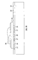
- FIGS. 3A and 3B show an embodiment of a chemical detection sensor system having multiple SERS chemical detection sensors.
- FIG. 4 is a cross-sectional view of an embodiment of a SERS chemical detection sensor.
- FIG. 5 is an enlarged view of a section of the SERS chemical detection sensor depicted in FIG. 4 .
- FIG. 6 is a surface profile of the roughened surface of the substrate used in the SERS chemical detection sensor of FIG. 4 .
- FIG. 7 represents the formation of a silane layer on surface of a glass substrate used in an embodiment of a SERS chemical detection sensor.
- FIG. 8 shows the formation of a self-assembled monolayer (SAM) layer on the metal islands bonded to a glass substrate in the manufacture of an embodiment of a SERS chemical detection sensor.
- SAM self-assembled monolayer
- FIG. 9 shows the application of the SERS chemical detection sensor in a Raman scattering system.
- FIG. 10 shows an example of the Raman spectra of a chemical detection sensor.
- FIG. 11 shows the Raman spectra of an embodiment of a SERS chemical detection sensor.
- FIG. 12 shows glass substrates mounted at an angle in a vapor deposition system in the manufacture of an embodiment of a SERS chemical detection sensor.
- FIG. 13 is a cross-sectioned view of an embodiment of a multilayered SERS chemical detection sensor prior to electrochemical etching.
- FIG. 14 shows an electrochemical cell for manufacturing an embodiment of a SERS chemical detection sensor.
- FIG. 15 is a graph representing one period of an oxidation-reduction cycle used to manufacture a SERS chemical detection sensor in the electrochemical cell of FIG. 14 .
- FIG. 16 is a cross-sectioned view of the multilayered SERS chemical detection sensor of FIG. 13 after the electrochemical etching.
- FIG. 17 shows an embodiment of a SERS chemical detection sensor system that includes SERS chemical detection sensors having a hydrogel layer.
- FIG. 18 shows an embodiment of a SERS chemical detection sensor system wherein each SERS chemical detection sensors includes a hydrogel layer and a pH sensor.
- FIG. 19 is a cross-sectional view of the SERS chemical detection sensor of FIG. 18 .
- FIG. 20 shows an embodiment of a SERS chemical detection sensor system wherein each SERS chemical detection sensors includes a hydrogel layer and a thermocouple.
- FIG. 21 is a cross-sectional view of the SERS chemical detection sensor of FIG. 20 .
- FIG. 22 shows an embodiment of a SERS chemical detection sensor system wherein each SERS chemical detection sensors includes a light emitting diode and a photodetector.
- FIG. 23 is a cross-sectional view of the SERS chemical detection sensor of FIG. 22 .
- An embodiment of a chemical detection sensor system includes multiple SERS chemical detection sensors that may be configured into an array.
- Each chemical detection sensor of the array is designed to react with a specific class of compounds and consists of a thiol-coated, SERS-active substrate.
- Thiol coatings are chosen that will chemically bond to an analyte that one is interested in detecting. Once an analyte binds to the thiol coating, the analyte may be identified and quantified by its characteristic Raman emissions.
- an array of SERS chemical detection sensors may be designed to detect one or more different classes of chemicals or analytes, depending upon the specific thiol coating employed.
- FIG. 1 shows SERS spectra of sulfate interaction with a cysteamine coated chemical detection sensor.
- Cysteamine has a quaternary ammonium group that forms an ion pair with sulfate ion.
- the sulfate compound is the analyte.
- FIG. 1 the evolution of the sulfate peak as it interacts with the coating is seen at a wavelength of about 1000 cm ⁇ 1 .
- the concentration response of the sulfate, shown in FIG. 2 may be used to quantify the amount of sulfate that reacted with the chemical detection sensor. In the example shown in FIG.
- the cysteamine coating reacts reversibly with sulfate ion. It is desirable for the analyte to irreversibly chemically react with the coating on the chemical detection sensor so as to form a new compound, that may be detected and quantified by its characteristic Raman spectral emission.
- the thiol coating on a SERS chemical detection sensor protects the SERS-active metal surface of the sensor from degradation due to oxidation.
- the chemical detection sensor may be employed to detect chemicals of environmental concern such as: drugs, explosives, and agents used in chemical warfare. Because many chemical reactions occur in water, one or more of the chemical detection sensors may include a hydrogel layer to allow the thiol coating to chemically react with specific analytes.
- the hydrogel layer may be formulated to contain the needed reagents to facilitate reaction between the analyte and the thiol coating.
- Each SERS chemical detection sensor is intended for a single use application.
- the chemical detection sensor system may be carried by a person who is conducting site inspections, left in a given area for a specified period of time, or mounted on a remotely operated vehicle such as a car, airplane, or robot. After exposure, the chemical detection sensor system may be taken into a laboratory where the individual SERS chemical detection sensors may be individually interrogated using a Raman-based spectroscopy system to identify the chemicals that have reacted with the thiol coatings of the various SERS chemical detection sensors. Interrogation of only those SERS chemical detection sensors that have undergone a chemical reaction may be determined by coupling a SERS chemical detection sensor to a particular chemical reaction sensor of the sensor array. If a chemical reaction occurs, the chemical reaction sensor associated with a specific SERS chemical detection sensor undergoes a state change that is indicative of a chemical reaction.
- Chemical detection sensor system 200 includes a support structure 203 , such as a printed circuit board; a module 202 that houses an array of SERS chemical detection sensors and is supported by the structure 203 ; multiple chemical reaction sensors 205 ; processor 206 ; optional global positioning system (GPS) 208 ; optional clock 210 ; and power source 212 , all or some of which may be supported by structure 203 .
- Power source 212 provides electrical power to each of global positioning system (GPS) 208 , clock 210 , and processor 206 via power line 215 .
- GPS global positioning system
- Each individual chemical reaction sensors 205 may be mounted in a fixing layer 224 formed on support structure 203 .
- fixing layer 224 may be formed of an epoxy, or any other substance typically used for affixing electrical components to a support structure.
- Chemical reaction sensors 205 are positioned in fixing layer 224 which is mounted between module 202 and support structure 203 .
- Each chemical reaction sensor 205 is disposed to detect a change in state when the specific SERS chemical detection sensor 204 undergoes a chemical reaction with the analyte. State changes for each sensor 205 are presented on a signal line 217 coupled between each SERS chemical detection sensor 204 and processor 206 .
- chemical reaction sensor 205 may be implemented as a thermocouple and/or a surface acoustic wave (SAW) device.
- SAW surface acoustic wave
- chemical reaction sensor 205 is disposed for detecting the heat transfer either to or from the SERS chemical detection sensor 204 that is operably coupled to that particular chemical reaction sensor 205 .
- the heat transfer is caused by a chemical reaction between the SERS chemical detection sensor 204 and an analyte.
- chemical reaction sensor 205 detects changes in the acoustic properties of a particular SERS chemical detection sensor 204 caused by a chemical reaction between the SERS chemical detection sensor and an analyte.
- processor 206 records an occurrence of a chemical reaction at one or more of the SERS chemical detection sensors 204 , based on sensing the state change that is detectable on one of the signal lines 217 .
- processor 206 may also record the specific time and/or position of the sensor 200 based on clock signal 214 generated by clock 210 , and global position signal 216 generated by GPS 208 in order to determine the time and location of the occurrence of particular chemical reactions detected by sensor 200 .
- the clock signal 214 represents a time value generated by clock 210
- global position signal 216 represents a global position value generated by GPS 208 .
- SERS chemical detection sensor 204 includes metal islands formed on the roughened surface of a transparent substrate such as transparent glass. When in contact with an analyte of interest and illuminated with appropriate excitation energy, a SERS chemical detection sensor will produce spectra having unique characteristics that are used to identify and quantify the amount of analyte detected.
- analytes may include organic, metallic, and anionic contaminants.
- SERS chemical detection sensor 204 includes a specially roughened surface 12 of a transparent substrate 14 , such as glass, on which an adhesion layer 15 is formed. Adhesion layer 15 promotes the bonding of the metal islands 16 to the glass substrate 14 .
- the metal islands 16 are formed, as for example, by vapor deposition, on adhesion layer 15 to create a metal patterned substrate 11 , shown in FIG. 8 .
- a thiol coating, or self-assembled monolayer 18 on metal islands 16 protects metal islands 16 from degradation, thereby extending the lifetime of chemical detection sensor 204 when exposed to air or aqueous environments from minutes or hours to months.
- the roughened surface 12 facilitates both a good SERS response and adhesion of the metal islands 16 to the substrate 14 .
- transparent substrate 14 such as a clear borosilicate glass slide, is carefully cleaned and prepared prior to having a metal film deposited on it.
- substrate 14 is immersed in a heated or boiling liquid reagent or reagents to remove any oils, metallic materials, and other contaminants that may be present on substrate 14 .
- a transparent substrate 14 may be immersed in boiling nitric acid for about 30 minutes.
- other liquid reagents also may be used such as hydrofluoric acid, hydrochloric acid, potassium hydroxide.
- substrate 14 is removed from the boiling nitric acid and rinsed in either deionized or distilled water.
- substrate 14 is immersed in hot or boiling methanol for about 30 minutes, followed by immersion in boiling acetone for about 30 minutes. This procedure removes any remaining organic contaminants. Substrate 14 is then removed from the methanol and allowed to air dry, as for example, about 1 hour.
- cleaned surface 12 of substrate 14 is etched to provide surface 12 with a surface roughness having a maximum peak to valley depth of about 16,000, an average peak to valley depth of about 2,500, and a peak-to-peak periodicity of about 12.5 microns.
- the roughness of surface 12 and its periodicity may be measured using a Dektak 3 ST Surface Profiler (Vecco Sloan Technology).
- commercial white glass generally has a surface having a peak to valley depth of about 200,000, an average peak to valley depth of about 43,700, and a peak-to-peak periodicity of about 100 microns.
- the combination of surface roughness and peak-to-peak periodicity of surface 12 provides SERS chemical detection sensor 204 with a greatly enhanced SERS response.
- surface 12 may be etched using a chemical etchant such as an HF based cream such as Velvet Etching Cream, manufactured by McKay International. Experience has shown that etching white glass for approximately 1 minute provides the surface roughness characteristics described above. Alternatively, surface 12 may be roughened using standard photo lithographic techniques.
- a chemical etchant such as an HF based cream such as Velvet Etching Cream, manufactured by McKay International.
- etching white glass for approximately 1 minute provides the surface roughness characteristics described above.
- surface 12 may be roughened using standard photo lithographic techniques.
- structure 14 is rinsed with distilled or deionized water, followed by an ethanol rinse.
- the cleaned, etched substrate 14 is then derivitized in a silanization agent such as a 1:10 mixture by volume of (3-mercaptopropyl) trimethoxysilane (MCTMS) in ethanol for about 24 hours to form adhesion layer 15 on roughened surface 12 .
- MTMS 3-mercaptopropyl trimethoxysilane
- FIG. 7 it is believed that the derivitization process causes a silane layer to bond to ⁇ OH functional groups believed to be present on surface 12 when substrate 14 is implemented as a transparent glass substrate.
- Substrate 14 was next rinsed in ethanol to remove unreacted (3-mercaptopropyl) trimethoxysilane and allowed to air dry.
- Adhesion layer 15 promotes bonding between roughened surface 12 and metal islands 16 .
- one or more cleaned substrates 14 are positioned so that they each rest on both a stainless steel spacer 84 and on support structure 82 in a vapor deposition system 80 so that roughened surfaces 12 face upwardly at a slight angle a with respect to the horizontal.
- the angle may be in the range, for example, of about 3–5 degrees, and more preferably, 4.5 degrees.
- the purpose of canting substrate 14 at an angle with respect to the horizontal is to create “shadows” that prevent the deposited metal that comprises metal islands 16 from forming a continuous metal layer on roughened or discontinuous surface 12 . Discontinuities on the surfaces of metal islands 16 have that have been shown to enhance the SERS response of SERS chemical detection sensor 204 .
- a metal such as gold, silver, or copper may be vapor deposited onto adhesion layer 15 to form metal islands 16 .
- gold islands were vapor deposited onto roughened surface 12 using material evaporated from an Aldrich, 99.99% pure gold wire.
- Vapor deposition system 80 may be implemented as a Vecco Model E.C. 200 vapor deposition system.
- adhesion layer 15 durably bonds metal islands 16 to roughened surface 12 so that SERS chemical detection sensor 204 may provide an effective SERS response after being immersed in an aqueous environment for months.
- a patterned metal structure 11 is created.
- Patterned metal structure 11 may be placed in a dilute ethanolic thiol solution at ambient temperature and pressure for a period of time, such as 24 hours. While metal structure 11 is immersed in the thiol solution, metal islands 16 react with the thiol to form a durable, self-assembled monolayer 18 on the metal islands 16 , as shown in FIG. 8 .
- Thiol coatings may be selected which have an affinity for the analyte (organic compounds, metal ions, or anions) of interest. Moreover, detection limits in the ppb to ppm range are possible.
- TABLE 1 provides, by way of example, a list of examples of thiols and analytes that may be detected using such thiol coatings. However, TABLE 1 is not to be considered exhaustive.
- Excitation light source 52 such as a Spectra Diode Laser, Inc. Model SDL-5712-H1
- Optical signal 54 emitted from excitation fiber 56 is collimated by lens 58 , such as a 6.4 mm focal length plano-convex lens manufactured by Newport, Model KPX010R.16.
- Interferences due to fiber Raman emissions may be removed by band pass filter 60 (Chroma Technology Part No.
- the interaction of excitation signal 54 and SERS chemical detection sensor 204 in the presence of an analyte of interest generally results in emission of Raman scattering signals 72 that are reflected by mirror 64 to lens 63 .
- Scattering signals 72 reflected by mirror 74 are directed through long pass filter 76 , such as a Chroma Technology, Part No. 852REF.
- Lens 78 focuses the scattered Raman emissions 72 into a 365 nm diameter collection optical fiber 80 .
- Fiber 80 directs Raman emissions 72 to Raman system 82 which may be implemented as a Chromex Raman One Spectrometer.
- the Raman system 82 converts the Raman emissions 72 into a Raman spectrum 84 .
- the Raman spectrum 84 from Raman system 82 is displayed and analyzed on a PC workstation 86 .
- FIGS. 10 and 11 show Raman spectra of p-thiocresol chemisorbed on a thin film of gold formed on glass substrates, referenced as a “SERS chemical detection sensor” for convenience.
- the horizontal axis in each of FIGS. 10 and 11 represent the wavelength of the emitted spectra.
- the vertical axis in each of FIGS. 10 and 11 represents optical intensity or number of photons emitted at 1073 cm ⁇ 1 detected with a Chromex Raman One Spectrometer using a diffraction grating having 600 grooves/mm and binning three horizontal pixels. The detector was operated at ⁇ 50 C, and had a 100 second CCD integration time.
- the SERS chemical detection sensors 204 were illuminated with an 852 nm DBR diode laser. Laser power at the sample was 63 mW.
- the element used to generate the curves in FIG. 10 included a layer of gold having a thickness of 151 that was formed on a commercial white glass substrate.
- Curve 90 represents the number of photons generated from a SERS chemical detection sensor having a glass surface untreated with MCTMS.
- Curve 92 represents the number of photons generated from a SERS chemical detection sensor having a gold layer formed on a glass surface treated with MCTMS.
- a SERS chemical detection sensor comprised of a gold layer formed on commercial white glass surface that is not treated with MCTMS exhibits a good SERS response, i.e., it emits a relatively high number of photons when illuminated as described.
- the gold film has very poor adhesion to such untreated surfaces and is very fragile. Treating a commercial white glass surface with MCTMS greatly improves the durability of the bond between the gold layer and the commercial white glass surface.
- the SERS response of the MCTMS surface results in a relatively poor SERS response as revealed by curve 92 of FIG. 10 .
- curve 94 represents the number of photons emitted from a SERS chemical detection sensor 204 having gold islands formed on a transparent glass surface that is untreated with MCTMS and which is etched in accordance with the teachings herein.
- Curve 96 represents the number of photons generated from SERS chemical detection sensor 204 having gold islands 16 that is manufactured in accordance with the teachings herein.
- the SERS response at 1073 cm ⁇ 1 as represented by curves 94 and 96 are indistinguishable.
- the SERS chemical detection sensor used to generate curve 94 has very fragile gold islands which were not bonded well to the glass substrate, whereas the SERS chemical detection sensor 204 used to generate curve 96 has very durable gold islands.
- the SERS chemical detection sensors described herein each have metal islands durably bonded to a glass substrate and exhibit an excellent SERS response.
- SERS chemical detection sensor 204 a that exhibits a good SERS response and is durable in an aqueous environment is manufactured using electrochemical techniques described with reference to FIGS. 13–16 .
- the fabrication of SERS chemical detection sensor 204 a starts by immersing substrate 14 a , such as clear, borosilicate glass in a heated or boiling liquid reagent or reagents such as nitric acid, hydrofluoric acid, hydrochloric acid, or potassium hydroxide, for about 30 minutes. Such immersion removes any oils, metallic materials, and other contaminants that may be present on substrate 14 a .
- substrate 14 a is removed from the boiling reagent and rinsed in either deionized or distilled water.
- substrate 14 a is immersed in hot or boiling methanol for about 30 minutes, followed by immersion in boiling acetone for about 30 minutes. This procedure removes any remaining organic contaminants. Substrate 14 a then is removed from the boiling methanol and allowed to air dry, as for example, about 1 hour.
- Cleaned substrate 14 a then is derivitized in a silanization agent such as a 1:10 mixture by volume of (3-mercaptopropyl) trimethoxysilane (MCTMS) and ethanol for about 24 hours to form adhesion layer 15 a on substrate 14 a .
- a silanization agent such as a 1:10 mixture by volume of (3-mercaptopropyl) trimethoxysilane (MCTMS) and ethanol for about 24 hours to form adhesion layer 15 a on substrate 14 a .
- Substrate 14 a next is rinsed in ethanol to remove unreacted (3-mercaptopropyl) trimethoxysilane and allowed to air dry.
- the metal coated SERS chemical detection sensor 204 a next is subjected to electro chemical techniques described with reference to FIG. 14 .
- Metal coated SERS chemical detection sensor 204 a is partially immersed in an electrochemical cell 111 that includes electrolyte 101 such as a 0 . 1 M solution of potassium chloride (KCl) held within fluid container 101 and electrodes 105 and 108 , and a working electrode 113 comprised of clamp 106 and the metallic layer 17 of metal coated SERS chemical detection sensor 204 a .
- electrolyte 101 such as a 0 . 1 M solution of potassium chloride (KCl) held within fluid container 101 and electrodes 105 and 108
- a working electrode 113 comprised of clamp 106 and the metallic layer 17 of metal coated SERS chemical detection sensor 204 a .
- Metal coated SERS chemical detection sensor 204 a is clamped to side 102 of fluid container 104 by metallic clamp 106 so that there is electrical continuity between clamp 106 and metal layer 17 . It is important that metallic clamp 106 not be immersed in the electrolyte 101 to prevent metallic ions from the clamp from contaminating the electrolyte. Also immersed in electrolyte 101 are counter electrode 105 and reference electrode 108 . Counter electrode 105 preferably is made of platinum wire 107 and platinum gauze 109 that is electrically and mechanically coupled to wire 107 . Electrode 105 is positioned so that gauze 109 is immersed in electrolyte 101 to increase the active surface area of electrode 105 in electrolyte 101 .
- Reference electrode 108 preferably is made of silver/silver chloride. Electrodes 105 and 108 , and clamp 106 are connected via wires 110 , 112 , and 114 , respectively, to potentiostat 116 . Potentiostat 116 maintains appropriate voltage levels at each of electrodes 105 and 108 , and, electrode 113 under the supervision of computer 118 via signal line 120 .
- the voltage, V W , of working electrode 113 is modulated from ⁇ 300 mV to 1200 mV with respect to the voltage of reference electrode 108 for a predetermined number of oxidative-reductive cycles.
- An example of an oxidative-reductive cycle is shown, by way of example, in FIG. 15 .
- V W is held at ⁇ 300 mV for about 30 seconds and then ramped to 1200 mV at a rate of about 500 mV/s.
- V W is held at 1200 mV for about 1.3 seconds and then reduced to ⁇ 300 mV at a rate of about ⁇ 500 mV/s.
- SERS chemical detection sensor 204 a transforms metal layer 17 into isolated metal islands 16 a having an average surface roughness of about 20 ⁇ , thereby creating a patterned metal SERS chemical detection sensor 204 a , as shown in FIG. 16 .
- SERS chemical detection sensor 204 a then may be placed in a dilute ethanolic thiol solution at ambient temperature and pressure for a period of time, such as 24 hours, so that the metal islands 16 a may react with a thiol to form a durable, self-assembled monolayer 18 on the metal islands 16 .
- Thiol coatings may be selected which have an affinity for the analyte (organic compounds, metal ions, or anions) of interest. Examples of suitable thiol coatings are identified in TABLE 1, above.
- each of the SERS chemical detection sensors 204 are fabricated in wells 230 formed in transparent substrate 14 , such as borosilicate glass.
- wells 230 may have 2.0 mm ⁇ 2.0 mm perimeters 232 and be spaced about 2.00 mm apart in a rectangular array as shown in FIG. 3 .
- SERS Chemical detection sensor 204 includes a specially roughened surface 12 in each well 230 of glass substrate 14 . Then an adhesion layer 15 is formed over the roughened surface 12 . Adhesion layer 15 promotes the bonding of the metal islands 16 to the glass substrate 14 .
- the metal islands 16 are formed, as for example, by vapor deposition, on adhesion layer 15 to create a metal patterned substrate 11 , shown in FIG. 8 .
- a thiol coating, or self-assembled monolayer 18 on metal islands 16 protects metal islands 16 from degradation, thereby extending the lifetime of SERS chemical detection sensor 204 when exposed to air or aqueous environments from minutes or hours to months.
- the roughened surface 12 facilitates both a good SERS response and adhesion of the metal islands 16 to the substrate 14 .
- a hydrogel layer 234 is formed over the self-assembled monolayer 18 and adhesion layer 15 .
- the hydrogel layer 234 should having a thickness sufficient to completely cover the self-assembled monolayer 18 , as for example, in the range of about 0.1 to 0.5 microns.
- the hydrogel layer 234 facilitates diffusion of an analyte towards the self-assembled monolayer of the SERS chemical detection sensor 204 and allows chemical reactions between the monolayer and analyte to occur in an aqueous environment.
- the hydrogel layer may contain additional reagents to facilitate the chemical reaction between the monolayer and analyte. Glass substrates having well structures suitable for use in conjunction with the disclosed embodiments may be obtained commercially from BioTrove in Cambridge, Mass.
- FIGS. 18 and 19 show an embodiment of a SERS chemical detection sensor system 200 includes a module 202 having multiple SERS chemical detection sensors 204 of which one or more may that include a pH sensor 242 .
- the pH sensors 242 are electrically coupled via electrodes 243 to electrical interconnect 254 .
- interconnect 254 is electrically coupled via signal line 254 to processor 206 .
- SERS chemical detection sensors 204 of module 202 further include a hydrogel layer 234 formed in well 230 of transparent substrate 14 .
- An end 247 of pH sensor 242 is coextensive with sidewall 233 of well 230 so that pH sensor 242 is in direct physical contact with the hydrogel layer 234 .
- electrodes 243 may be fabricated from electrically conductive materials such as aluminum, silver, copper, and gold. Electrodes 243 may also be made of electrically conductive polymers.
- An electrical insulating layer 256 which may consist essentially of silicon dioxide, is formed over each pH sensor 242 and its associated electrodes 243 to secure and maintain the position of pH sensors 242 in the module 202 . Because FIG.
- FIG. 19 provides an elevation view of SERS chemical detection sensor 204 , only a single electrode 243 is shown associated with each SERS chemical detection sensor 204 . However, it is to be understood that one or more electrodes 243 may be coextensive with side wall 233 of each SERS chemical detection sensor 204 .
- electrodes 250 may be directly coupled to processor 206 , so that the processor may determine the electrical conductivity between electrodes 250 of a particular SERS chemical detection sensor 204 .
- the electrical conductivity of hydrogel layer 234 may change when a chemical reaction occurs in any of SERS chemical detection sensors 204 . Such change in the electrical conductivity may be sensed as a change of state of the conductivity of the hydro gel layer 234 by processor 204 and recorded.
- each of SERS chemical detection sensors 204 includes a pair of electrodes 250 .
- each of SERS chemical detection sensors 204 includes a thermocouple 271 that is operably coupled through interconnect 254 to processor 206 via signal line 260 .
- the temperature of the hydrogel layer 234 of that particular SERS chemical detection sensor 204 changes, i.e., changes state.
- the temperature change is sensed by a thermocouple 272 and recorded by processor 206 .
- thermocouple 271 may be fabricated from two dissimilar electrically conductive materials that define wire connects 274 and 276 that are in contact with each other at sidewall 233 .
- An electrical insulating layer 256 which may consist essentially of silicon dioxide, is formed over thermocouples 271 .
- thermocouples 271 is cardinally related to the number of SERS chemical detection sensors 204 of module 202 . From the above, it may be appreciated that pH sensors 242 , electrodes 243 , and thermocouple 271 all comprise elements of various types of a chemical reaction sensor 205 .
- each of SERS chemical detection sensors 204 includes a chemical reaction sensor 205 that comprises a light emitting diode (LED) 270 and photodetector 272 attached to transparent substrate 14 opposite self-assembled monolayer 18 .
- the light emitting diodes 270 and photodetectors 272 may be fabricated in substrate 14 using photo lithographic techniques. Electrical power to the light emitting diodes 270 and photodetectors 272 is provided by power source 212 through interconnect 254 A via signal line 215 .
- LED 270 emits an excitation light signal 280 that is directed towards self-assembled monolayer 18 .
- the light signal 282 that is reflected off of metal islands 16 may have different wavelength characteristics than those of excitation light signal 280 .
- the difference in the wavelength characteristics between excitation light signal 280 and light signal 282 is believed to be due to a plasmon effect that occurs at the self-assembled monolayer. It is believed that the plasmon effect results from the change in molecular weight of the thiol that comprises the self-assembled monolayer when a chemical reaction occurs there.
- Photodetector 276 may be selected to be sensitive to a narrow band about the wavelength of light signal 282 that results from the occurrence of a particular chemical reaction at the self-assembled monolayer 18 of a specific chemical detection sensor 204 .
- photodetector 276 Upon detection of light signal 282 , photodetector 276 generates a signal 276 that is provided to processor 206 via interconnect 254 B. Signal 276 indicates whether photodetector 276 , and hence chemical reaction sensor 205 has undergone a state change. Processor 206 then stores information that represents the occurrence of a particular type of chemical reaction at a specific chemical reaction sensor 204 .
Abstract
Description
| TABLE 1 | |
| Thiol Type: | Useful For Detecting: |
| 1-propanethiol | Benzene, toluene, ethylbenzene, |
| xylene) and chlorinated solvents | |
| cysteamine hydrochloride | anions such as nitrate and sulfate |
| 4-(2-pyridylazo) resorcinol modified | Pb++, Cd++, and Cu++ |
| with a disulfide group | |
| thiol derivatized dibenzo 18-crown-6 | alkali metals |
Claims (23)
Priority Applications (1)
| Application Number | Priority Date | Filing Date | Title |
|---|---|---|---|
| US10/294,655 US7022288B1 (en) | 2002-11-13 | 2002-11-13 | Chemical detection sensor system |
Applications Claiming Priority (1)
| Application Number | Priority Date | Filing Date | Title |
|---|---|---|---|
| US10/294,655 US7022288B1 (en) | 2002-11-13 | 2002-11-13 | Chemical detection sensor system |
Publications (1)
| Publication Number | Publication Date |
|---|---|
| US7022288B1 true US7022288B1 (en) | 2006-04-04 |
Family
ID=36101898
Family Applications (1)
| Application Number | Title | Priority Date | Filing Date |
|---|---|---|---|
| US10/294,655 Expired - Fee Related US7022288B1 (en) | 2002-11-13 | 2002-11-13 | Chemical detection sensor system |
Country Status (1)
| Country | Link |
|---|---|
| US (1) | US7022288B1 (en) |
Cited By (65)
| Publication number | Priority date | Publication date | Assignee | Title |
|---|---|---|---|---|
| US20050157304A1 (en) * | 2004-01-20 | 2005-07-21 | General Electric Company | Handheld device with a disposable element for chemical analysis of multiple analytes |
| US20060101927A1 (en) * | 2004-11-18 | 2006-05-18 | Blakeley Gerald W Iii | Analytical measurement meters with location determination capability |
| US20060133960A1 (en) * | 2003-04-28 | 2006-06-22 | Ahmad Lubna M | Thermoelectric sensor for analytes in a gas |
| US20060164636A1 (en) * | 2005-01-27 | 2006-07-27 | Islam M S | Integrated modular system and method for enhanced Raman spectroscopy |
| US20070035729A1 (en) * | 2005-08-11 | 2007-02-15 | Leona Marco | Non-Invasive Identification of Fluorescent Dyes in Historic Textiles By Matrix Transfer-Surface Enhanced Raman Scattering |
| US20070124175A1 (en) * | 2005-11-30 | 2007-05-31 | Searete Llc, A Limited Liability Corporation Of The State Of Delaware. | Computational and/or control systems and methods related to nutraceutical agent selection and dosing |
| US20070124176A1 (en) * | 2005-11-30 | 2007-05-31 | Searete Llc, A Limited Liability Corporation Of The State Of Delaware | Computational and/or control systems and methods related to nutraceutical agent selection and dosing |
| US20070124218A1 (en) * | 2005-11-30 | 2007-05-31 | Searete Llc, A Limited Liability Corporation Of The State Of Delaware | Computational and/or control systems related to individualized nutraceutical selection and packaging |
| US20070136092A1 (en) * | 2005-11-30 | 2007-06-14 | Searete Llc, A Limited Liability Corporation Of The State Of Delaware | Computational and/or control systems related to individualized pharmaceutical and nutraceutical selection and packaging |
| US20070214008A1 (en) * | 2005-11-30 | 2007-09-13 | Searete Llc, A Limited Liability Corporation Of The State Delaware | Computational and/or control systems and methods related to nutraceutical agent selection and dosing |
| US20080003307A1 (en) * | 2006-06-28 | 2008-01-03 | Searete Llc, A Limited Liability Corporation Of The State Of Delaware | Methods and systems for analysis of nutraceutical associated components |
| US20080046395A1 (en) * | 2005-11-30 | 2008-02-21 | Searete Llc, A Limited Liability Corporation Of The State Of Delaware | Computational systems and methods related to nutraceuticals |
| US20080047230A1 (en) * | 2006-06-14 | 2008-02-28 | Searete Llc, A Limited Liability Corporation Of The State Of Delaware | Individualized pharmaceutical selection and packaging |
| US20080053193A1 (en) * | 2003-04-28 | 2008-03-06 | Ahmad Lubna M | Thermoelectric sensor for analytes in a gas and related method |
| US20080053194A1 (en) * | 2003-04-28 | 2008-03-06 | Ahmad Lubna M | Thermoelectric sensor for analytes in a gas and related method |
| US20080094620A1 (en) * | 2006-10-20 | 2008-04-24 | Zhiyong Li | Systems and methods for detection of Raman scattered photons |
| US20080183396A1 (en) * | 2005-11-30 | 2008-07-31 | Searete Llc, A Limited Libility Corporation Of The State Of Delaware | Systems and methods for transmitting pathogen related information and responding |
| US20090097021A1 (en) * | 2005-10-25 | 2009-04-16 | Kyushu University, National University Corporation | Substrate and Substrate Assembly for Use in Raman Spectroscopic Analysis |
| US7827042B2 (en) | 2005-11-30 | 2010-11-02 | The Invention Science Fund I, Inc | Methods and systems related to transmission of nutraceutical associated information |
| CN101034083B (en) * | 2007-03-12 | 2011-01-26 | 清华大学 | Manufacturing method of sonic surface wave gas sensor |
| US7879625B1 (en) | 2008-12-03 | 2011-02-01 | The United States Of America As Represented By The Secretary Of The Navy | Preparation of SERS substrates on silica-coated magnetic microspheres |
| US20110125408A1 (en) * | 2003-04-28 | 2011-05-26 | Ahmad Lubna M | Thermoelectric biosensor for analytes in a gas |
| US7974856B2 (en) | 2005-11-30 | 2011-07-05 | The Invention Science Fund I, Llc | Computational systems and methods related to nutraceuticals |
| US8000981B2 (en) | 2005-11-30 | 2011-08-16 | The Invention Science Fund I, Llc | Methods and systems related to receiving nutraceutical associated information |
| US20110230375A1 (en) * | 2006-12-14 | 2011-09-22 | Life Technologies Corporation | Methods and apparatus for measuring analytes using large scale fet arrays |
| US20120001779A1 (en) * | 2010-06-30 | 2012-01-05 | Life Technologies Corporation | Serializer circuit |
| WO2012013937A1 (en) * | 2010-07-30 | 2012-02-02 | Queen Mary & Westfield College | Sensor coasting layer, device and method |
| CN102879378A (en) * | 2011-07-13 | 2013-01-16 | 赛默科技便携式分析仪器有限公司 | Heroin detection by raman spectroscopy from impure compositions comprising an interfering fluorescent contaminant |
| US8441044B2 (en) | 2006-12-14 | 2013-05-14 | Life Technologies Corporation | Methods for manufacturing low noise chemically-sensitive field effect transistors |
| US8524057B2 (en) | 2008-06-25 | 2013-09-03 | Life Technologies Corporation | Methods and apparatus for measuring analytes using large scale FET arrays |
| US8552771B1 (en) | 2012-05-29 | 2013-10-08 | Life Technologies Corporation | System for reducing noise in a chemical sensor array |
| US8592153B1 (en) | 2009-05-29 | 2013-11-26 | Life Technologies Corporation | Methods for manufacturing high capacitance microwell structures of chemically-sensitive sensors |
| US8653567B2 (en) | 2010-07-03 | 2014-02-18 | Life Technologies Corporation | Chemically sensitive sensor with lightly doped drains |
| US8685324B2 (en) | 2010-09-24 | 2014-04-01 | Life Technologies Corporation | Matched pair transistor circuits |
| US8722417B2 (en) | 2003-04-28 | 2014-05-13 | Invoy Technologies, L.L.C. | Thermoelectric sensor for analytes in a fluid and related method |
| US8747748B2 (en) | 2012-01-19 | 2014-06-10 | Life Technologies Corporation | Chemical sensor with conductive cup-shaped sensor surface |
| US8776573B2 (en) | 2009-05-29 | 2014-07-15 | Life Technologies Corporation | Methods and apparatus for measuring analytes |
| EP2769214A1 (en) * | 2011-10-18 | 2014-08-27 | Hewlett-Packard Development Company, L.P. | Molecular sensing device |
| US8821798B2 (en) | 2012-01-19 | 2014-09-02 | Life Technologies Corporation | Titanium nitride as sensing layer for microwell structure |
| US8841217B1 (en) | 2013-03-13 | 2014-09-23 | Life Technologies Corporation | Chemical sensor with protruded sensor surface |
| US8858782B2 (en) | 2010-06-30 | 2014-10-14 | Life Technologies Corporation | Ion-sensing charge-accumulation circuits and methods |
| US8936763B2 (en) | 2008-10-22 | 2015-01-20 | Life Technologies Corporation | Integrated sensor arrays for biological and chemical analysis |
| US8962366B2 (en) | 2013-01-28 | 2015-02-24 | Life Technologies Corporation | Self-aligned well structures for low-noise chemical sensors |
| US8963216B2 (en) | 2013-03-13 | 2015-02-24 | Life Technologies Corporation | Chemical sensor with sidewall spacer sensor surface |
| US20150190804A1 (en) * | 2010-10-12 | 2015-07-09 | Stmicroelectronics, Inc. | Silicon substrate optimization for microarray technology |
| US9080968B2 (en) | 2013-01-04 | 2015-07-14 | Life Technologies Corporation | Methods and systems for point of use removal of sacrificial material |
| US9116117B2 (en) | 2013-03-15 | 2015-08-25 | Life Technologies Corporation | Chemical sensor with sidewall sensor surface |
| US9128044B2 (en) | 2013-03-15 | 2015-09-08 | Life Technologies Corporation | Chemical sensors with consistent sensor surface areas |
| US9404920B2 (en) | 2006-12-14 | 2016-08-02 | Life Technologies Corporation | Methods and apparatus for detecting molecular interactions using FET arrays |
| US9618475B2 (en) | 2010-09-15 | 2017-04-11 | Life Technologies Corporation | Methods and apparatus for measuring analytes |
| US9671363B2 (en) | 2013-03-15 | 2017-06-06 | Life Technologies Corporation | Chemical sensor with consistent sensor surface areas |
| US9823217B2 (en) | 2013-03-15 | 2017-11-21 | Life Technologies Corporation | Chemical device with thin conductive element |
| US9835585B2 (en) | 2013-03-15 | 2017-12-05 | Life Technologies Corporation | Chemical sensor with protruded sensor surface |
| US9841398B2 (en) | 2013-01-08 | 2017-12-12 | Life Technologies Corporation | Methods for manufacturing well structures for low-noise chemical sensors |
| US9970984B2 (en) | 2011-12-01 | 2018-05-15 | Life Technologies Corporation | Method and apparatus for identifying defects in a chemical sensor array |
| US10077472B2 (en) | 2014-12-18 | 2018-09-18 | Life Technologies Corporation | High data rate integrated circuit with power management |
| US10100357B2 (en) | 2013-05-09 | 2018-10-16 | Life Technologies Corporation | Windowed sequencing |
| US10379079B2 (en) | 2014-12-18 | 2019-08-13 | Life Technologies Corporation | Methods and apparatus for measuring analytes using large scale FET arrays |
| US10451585B2 (en) | 2009-05-29 | 2019-10-22 | Life Technologies Corporation | Methods and apparatus for measuring analytes |
| US10458942B2 (en) | 2013-06-10 | 2019-10-29 | Life Technologies Corporation | Chemical sensor array having multiple sensors per well |
| US10605767B2 (en) | 2014-12-18 | 2020-03-31 | Life Technologies Corporation | High data rate integrated circuit with transmitter configuration |
| EP3696536A1 (en) * | 2015-04-14 | 2020-08-19 | Illumina, Inc. | A method of manufacturing a substrate and a method of analyzing biomolecules capable of generating light emissions |
| US11231451B2 (en) | 2010-06-30 | 2022-01-25 | Life Technologies Corporation | Methods and apparatus for testing ISFET arrays |
| US11307166B2 (en) | 2010-07-01 | 2022-04-19 | Life Technologies Corporation | Column ADC |
| US11339430B2 (en) | 2007-07-10 | 2022-05-24 | Life Technologies Corporation | Methods and apparatus for measuring analytes using large scale FET arrays |
Citations (23)
| Publication number | Priority date | Publication date | Assignee | Title |
|---|---|---|---|---|
| US4781458A (en) | 1987-11-30 | 1988-11-01 | The United States Of America As Represented By The United States Department Of Energy | Fiber optic apparatus for detecting molecular species by surface enhanced Raman spectroscopy |
| US5010776A (en) | 1989-05-04 | 1991-04-30 | Iit Research Institute | Environmental contamination detection and analyzing system and method |
| US5112127A (en) | 1989-11-28 | 1992-05-12 | Eic Laboratories, Inc. | Apparatus for measuring Raman spectra over optical fibers |
| US5194913A (en) | 1991-03-20 | 1993-03-16 | The United States Of America As Represented By The United States Department Of Energy | Fiber-optic apparatus and method for measurement of luminescence and raman scattering |
| US5241368A (en) | 1991-01-07 | 1993-08-31 | Custom Sample Systems, Inc. | Fiber-optic probe for absorbance and turbidity measurement |
| US5255067A (en) * | 1990-11-30 | 1993-10-19 | Eic Laboratories, Inc. | Substrate and apparatus for surface enhanced Raman spectroscopy |
| US5327211A (en) * | 1991-11-07 | 1994-07-05 | Carron Keith T | Process for molecular-specific optical fiber probes for raman detection |
| US5376556A (en) | 1989-10-27 | 1994-12-27 | Abbott Laboratories | Surface-enhanced Raman spectroscopy immunoassay |
| US5402508A (en) | 1993-05-04 | 1995-03-28 | The United States Of America As Represented By The United States Department Of Energy | Fiber optic probe having fibers with endfaces formed for improved coupling efficiency and method using same |
| US5721102A (en) * | 1995-10-13 | 1998-02-24 | Lockheed Martin Energy Systems, Inc. | Surface enhanced Raman gene probe and methods thereof |
| US5739536A (en) | 1995-12-14 | 1998-04-14 | The United States Of America As Represented By The Secretary Of The Navy | Fiber optic infrared cone penetrometer system |
| US5759859A (en) | 1996-07-15 | 1998-06-02 | United States Of America As Represented By The Secretary Of The Army | Sensor and method for detecting trace underground energetic materials |
| US5774610A (en) | 1996-07-08 | 1998-06-30 | Equitech Int'l Corporation | Fiber optic probe |
| US5864397A (en) | 1997-09-15 | 1999-01-26 | Lockheed Martin Energy Research Corporation | Surface-enhanced raman medical probes and system for disease diagnosis and drug testing |
| US6018389A (en) | 1996-07-22 | 2000-01-25 | The Regents Of The University Of California | Cone penetrometer fiber optic raman spectroscopy probe assembly |
| US6028666A (en) | 1998-11-19 | 2000-02-22 | The United States Of America As Represented By The Secretary Of The Navy | Fiber optic Raman sensor |
| US6040191A (en) * | 1996-06-13 | 2000-03-21 | Grow; Ann E. | Raman spectroscopic method for determining the ligand binding capacity of biologicals |
| US6406777B1 (en) | 2000-06-14 | 2002-06-18 | The United States Of America As Represented By The Secretary Of The Navy | Metal and glass structure for use in surface enhanced Raman spectroscopy and method for fabricating same |
| US6558956B1 (en) * | 1997-06-24 | 2003-05-06 | The University Of Wyoming | Method and apparatus for detection of a controlled substance |
| US6614523B1 (en) * | 2000-06-14 | 2003-09-02 | The United States Of America As Represented By The Secretary Of The Navy | Sensor for performing surface enhanced Raman spectroscopy |
| US6649683B2 (en) * | 1999-04-06 | 2003-11-18 | Avalon Instruments Limited | Solid matrices for surface-enhanced raman spectroscopy |
| US6743581B1 (en) * | 1999-01-25 | 2004-06-01 | Ut-Battelle, Lc | Multifunctional and multispectral biosensor devices and methods of use |
| US6750065B1 (en) * | 1998-02-26 | 2004-06-15 | University Of Strathclyde | Immunoassays involving surface enhanced Raman scattering |
-
2002
- 2002-11-13 US US10/294,655 patent/US7022288B1/en not_active Expired - Fee Related
Patent Citations (24)
| Publication number | Priority date | Publication date | Assignee | Title |
|---|---|---|---|---|
| US4781458A (en) | 1987-11-30 | 1988-11-01 | The United States Of America As Represented By The United States Department Of Energy | Fiber optic apparatus for detecting molecular species by surface enhanced Raman spectroscopy |
| US5010776A (en) | 1989-05-04 | 1991-04-30 | Iit Research Institute | Environmental contamination detection and analyzing system and method |
| US5376556A (en) | 1989-10-27 | 1994-12-27 | Abbott Laboratories | Surface-enhanced Raman spectroscopy immunoassay |
| US5112127A (en) | 1989-11-28 | 1992-05-12 | Eic Laboratories, Inc. | Apparatus for measuring Raman spectra over optical fibers |
| US5255067A (en) * | 1990-11-30 | 1993-10-19 | Eic Laboratories, Inc. | Substrate and apparatus for surface enhanced Raman spectroscopy |
| US5241368A (en) | 1991-01-07 | 1993-08-31 | Custom Sample Systems, Inc. | Fiber-optic probe for absorbance and turbidity measurement |
| US5194913A (en) | 1991-03-20 | 1993-03-16 | The United States Of America As Represented By The United States Department Of Energy | Fiber-optic apparatus and method for measurement of luminescence and raman scattering |
| US5327211A (en) * | 1991-11-07 | 1994-07-05 | Carron Keith T | Process for molecular-specific optical fiber probes for raman detection |
| US5402508A (en) | 1993-05-04 | 1995-03-28 | The United States Of America As Represented By The United States Department Of Energy | Fiber optic probe having fibers with endfaces formed for improved coupling efficiency and method using same |
| US5721102A (en) * | 1995-10-13 | 1998-02-24 | Lockheed Martin Energy Systems, Inc. | Surface enhanced Raman gene probe and methods thereof |
| US5814516A (en) * | 1995-10-13 | 1998-09-29 | Lockheed Martin Energy Systems, Inc. | Surface enhanced Raman gene probe and methods thereof |
| US5739536A (en) | 1995-12-14 | 1998-04-14 | The United States Of America As Represented By The Secretary Of The Navy | Fiber optic infrared cone penetrometer system |
| US6040191A (en) * | 1996-06-13 | 2000-03-21 | Grow; Ann E. | Raman spectroscopic method for determining the ligand binding capacity of biologicals |
| US5774610A (en) | 1996-07-08 | 1998-06-30 | Equitech Int'l Corporation | Fiber optic probe |
| US5759859A (en) | 1996-07-15 | 1998-06-02 | United States Of America As Represented By The Secretary Of The Army | Sensor and method for detecting trace underground energetic materials |
| US6018389A (en) | 1996-07-22 | 2000-01-25 | The Regents Of The University Of California | Cone penetrometer fiber optic raman spectroscopy probe assembly |
| US6558956B1 (en) * | 1997-06-24 | 2003-05-06 | The University Of Wyoming | Method and apparatus for detection of a controlled substance |
| US5864397A (en) | 1997-09-15 | 1999-01-26 | Lockheed Martin Energy Research Corporation | Surface-enhanced raman medical probes and system for disease diagnosis and drug testing |
| US6750065B1 (en) * | 1998-02-26 | 2004-06-15 | University Of Strathclyde | Immunoassays involving surface enhanced Raman scattering |
| US6028666A (en) | 1998-11-19 | 2000-02-22 | The United States Of America As Represented By The Secretary Of The Navy | Fiber optic Raman sensor |
| US6743581B1 (en) * | 1999-01-25 | 2004-06-01 | Ut-Battelle, Lc | Multifunctional and multispectral biosensor devices and methods of use |
| US6649683B2 (en) * | 1999-04-06 | 2003-11-18 | Avalon Instruments Limited | Solid matrices for surface-enhanced raman spectroscopy |
| US6406777B1 (en) | 2000-06-14 | 2002-06-18 | The United States Of America As Represented By The Secretary Of The Navy | Metal and glass structure for use in surface enhanced Raman spectroscopy and method for fabricating same |
| US6614523B1 (en) * | 2000-06-14 | 2003-09-02 | The United States Of America As Represented By The Secretary Of The Navy | Sensor for performing surface enhanced Raman spectroscopy |
Non-Patent Citations (10)
| Title |
|---|
| Adsorption of Chlorinated Ethylenes at 1-Octadecanethiol-Modified Silver Surfaces, Analytical Chemistry, vol. 66, No. 4 Feb. 15, 1994, Mullen, K. et al, 478-483. |
| Carrabba, M. M. et al, Proceedings-Electrochemical Society 1993, 93-7, 634-642. * |
| Carron, K. et al, Environmental Science andTechnology 1992, 26, 1950-1954. * |
| Carron, K. T. et al, Analytical Chemistry 1995, 67, 3353-3356. * |
| Crane, L. G. et al, Analytical Chemistry 1995, 67, 360-634. * |
| Ehler, T. T. et al, Journal of Physical Chemistry B 1997, 101, 3174-3180. * |
| Lee, Y.-H. et al, SPIE 1999, 3857, 76-84. * |
| Long fiber-optic remote Raman probe for detection and identification of weak scatterers, Dec. 20, 1992/vol. 31, No. 36/ Applied Optics, Schoen, C.L. et al, 7707-7715. |
| Storey, J.M.E et al, Electrochemical SERS Detection of Chlorinated Hydrocarbons in Aquenous Solutions, vol. 48, No. 10, 1994 Applied Spectrocopy, 1265-1271. |
| Yonzon, C. R. et al, SPIE 2003, 5224, 78-85. * |
Cited By (160)
| Publication number | Priority date | Publication date | Assignee | Title |
|---|---|---|---|---|
| US20080053193A1 (en) * | 2003-04-28 | 2008-03-06 | Ahmad Lubna M | Thermoelectric sensor for analytes in a gas and related method |
| US20060133960A1 (en) * | 2003-04-28 | 2006-06-22 | Ahmad Lubna M | Thermoelectric sensor for analytes in a gas |
| US8722417B2 (en) | 2003-04-28 | 2014-05-13 | Invoy Technologies, L.L.C. | Thermoelectric sensor for analytes in a fluid and related method |
| US8088333B2 (en) | 2003-04-28 | 2012-01-03 | Invoy Technology, LLC | Thermoelectric sensor for analytes in a gas |
| US20110125408A1 (en) * | 2003-04-28 | 2011-05-26 | Ahmad Lubna M | Thermoelectric biosensor for analytes in a gas |
| US9429578B2 (en) | 2003-04-28 | 2016-08-30 | Invoy Technologies, Llc | Thermoelectric sensor for analytes in a gas and related method |
| US20080053194A1 (en) * | 2003-04-28 | 2008-03-06 | Ahmad Lubna M | Thermoelectric sensor for analytes in a gas and related method |
| US20050157304A1 (en) * | 2004-01-20 | 2005-07-21 | General Electric Company | Handheld device with a disposable element for chemical analysis of multiple analytes |
| US7283245B2 (en) * | 2004-01-20 | 2007-10-16 | General Electric Company | Handheld device with a disposable element for chemical analysis of multiple analytes |
| US20060101927A1 (en) * | 2004-11-18 | 2006-05-18 | Blakeley Gerald W Iii | Analytical measurement meters with location determination capability |
| US20060164636A1 (en) * | 2005-01-27 | 2006-07-27 | Islam M S | Integrated modular system and method for enhanced Raman spectroscopy |
| US7385691B2 (en) * | 2005-01-27 | 2008-06-10 | Hewlett-Packard Development Company, L.P. | Integrated modular system and method for enhanced Raman spectroscopy |
| US7362431B2 (en) | 2005-08-11 | 2008-04-22 | The Metropolitan Museum Of Art | Non-invasive identification of fluorescent dyes in historic textiles by matrix transfer-surface enhanced Raman scattering |
| US20070035729A1 (en) * | 2005-08-11 | 2007-02-15 | Leona Marco | Non-Invasive Identification of Fluorescent Dyes in Historic Textiles By Matrix Transfer-Surface Enhanced Raman Scattering |
| US20090097021A1 (en) * | 2005-10-25 | 2009-04-16 | Kyushu University, National University Corporation | Substrate and Substrate Assembly for Use in Raman Spectroscopic Analysis |
| US20070136092A1 (en) * | 2005-11-30 | 2007-06-14 | Searete Llc, A Limited Liability Corporation Of The State Of Delaware | Computational and/or control systems related to individualized pharmaceutical and nutraceutical selection and packaging |
| US20070124218A1 (en) * | 2005-11-30 | 2007-05-31 | Searete Llc, A Limited Liability Corporation Of The State Of Delaware | Computational and/or control systems related to individualized nutraceutical selection and packaging |
| US8340944B2 (en) | 2005-11-30 | 2012-12-25 | The Invention Science Fund I, Llc | Computational and/or control systems and methods related to nutraceutical agent selection and dosing |
| US20070214008A1 (en) * | 2005-11-30 | 2007-09-13 | Searete Llc, A Limited Liability Corporation Of The State Delaware | Computational and/or control systems and methods related to nutraceutical agent selection and dosing |
| US20080046395A1 (en) * | 2005-11-30 | 2008-02-21 | Searete Llc, A Limited Liability Corporation Of The State Of Delaware | Computational systems and methods related to nutraceuticals |
| US20080183396A1 (en) * | 2005-11-30 | 2008-07-31 | Searete Llc, A Limited Libility Corporation Of The State Of Delaware | Systems and methods for transmitting pathogen related information and responding |
| US20070124175A1 (en) * | 2005-11-30 | 2007-05-31 | Searete Llc, A Limited Liability Corporation Of The State Of Delaware. | Computational and/or control systems and methods related to nutraceutical agent selection and dosing |
| US7827042B2 (en) | 2005-11-30 | 2010-11-02 | The Invention Science Fund I, Inc | Methods and systems related to transmission of nutraceutical associated information |
| US8068991B2 (en) | 2005-11-30 | 2011-11-29 | The Invention Science Fund I, Llc | Systems and methods for transmitting pathogen related information and responding |
| US10296720B2 (en) | 2005-11-30 | 2019-05-21 | Gearbox Llc | Computational systems and methods related to nutraceuticals |
| US8000981B2 (en) | 2005-11-30 | 2011-08-16 | The Invention Science Fund I, Llc | Methods and systems related to receiving nutraceutical associated information |
| US20070124176A1 (en) * | 2005-11-30 | 2007-05-31 | Searete Llc, A Limited Liability Corporation Of The State Of Delaware | Computational and/or control systems and methods related to nutraceutical agent selection and dosing |
| US7974856B2 (en) | 2005-11-30 | 2011-07-05 | The Invention Science Fund I, Llc | Computational systems and methods related to nutraceuticals |
| US8297028B2 (en) | 2006-06-14 | 2012-10-30 | The Invention Science Fund I, Llc | Individualized pharmaceutical selection and packaging |
| US20080047230A1 (en) * | 2006-06-14 | 2008-02-28 | Searete Llc, A Limited Liability Corporation Of The State Of Delaware | Individualized pharmaceutical selection and packaging |
| US7927787B2 (en) | 2006-06-28 | 2011-04-19 | The Invention Science Fund I, Llc | Methods and systems for analysis of nutraceutical associated components |
| US20080003307A1 (en) * | 2006-06-28 | 2008-01-03 | Searete Llc, A Limited Liability Corporation Of The State Of Delaware | Methods and systems for analysis of nutraceutical associated components |
| US7405822B2 (en) * | 2006-10-20 | 2008-07-29 | Hewlett-Packard Development Company, L.P. | Systems and methods for detection of Raman scattered photons |
| US20080094620A1 (en) * | 2006-10-20 | 2008-04-24 | Zhiyong Li | Systems and methods for detection of Raman scattered photons |
| US8496802B2 (en) | 2006-12-14 | 2013-07-30 | Life Technologies Corporation | Methods for operating chemically-sensitive sample and hold sensors |
| US9404920B2 (en) | 2006-12-14 | 2016-08-02 | Life Technologies Corporation | Methods and apparatus for detecting molecular interactions using FET arrays |
| US11732297B2 (en) * | 2006-12-14 | 2023-08-22 | Life Technologies Corporation | Methods and apparatus for measuring analytes using large scale FET arrays |
| US8435395B2 (en) | 2006-12-14 | 2013-05-07 | Life Technologies Corporation | Methods and apparatus for measuring analytes using large scale FET arrays |
| US8441044B2 (en) | 2006-12-14 | 2013-05-14 | Life Technologies Corporation | Methods for manufacturing low noise chemically-sensitive field effect transistors |
| US8450781B2 (en) | 2006-12-14 | 2013-05-28 | Life Technologies Corporation | Methods and apparatus for measuring analytes using large scale FET arrays |
| US20110230375A1 (en) * | 2006-12-14 | 2011-09-22 | Life Technologies Corporation | Methods and apparatus for measuring analytes using large scale fet arrays |
| US8492800B2 (en) | 2006-12-14 | 2013-07-23 | Life Technologies Corporation | Chemically sensitive sensors with sample and hold capacitors |
| US9134269B2 (en) | 2006-12-14 | 2015-09-15 | Life Technologies Corporation | Methods and apparatus for measuring analytes using large scale FET arrays |
| US8519448B2 (en) | 2006-12-14 | 2013-08-27 | Life Technologies Corporation | Chemically-sensitive array with active and reference sensors |
| US10502708B2 (en) | 2006-12-14 | 2019-12-10 | Life Technologies Corporation | Chemically-sensitive sensor array calibration circuitry |
| US8530941B2 (en) | 2006-12-14 | 2013-09-10 | Life Technologies Corporation | Methods and apparatus for measuring analytes using large scale FET arrays |
| US8535513B2 (en) | 2006-12-14 | 2013-09-17 | Life Technologies Corporation | Methods and apparatus for measuring analytes using large scale FET arrays |
| US20220340965A1 (en) * | 2006-12-14 | 2022-10-27 | Life Technologies Corporation | Methods and Apparatus for Measuring Analytes Using Large Scale FET Arrays |
| US8558288B2 (en) | 2006-12-14 | 2013-10-15 | Life Technologies Corporation | Methods and apparatus for measuring analytes using large scale FET arrays |
| US8575664B2 (en) | 2006-12-14 | 2013-11-05 | Life Technologies Corporation | Chemically-sensitive sensor array calibration circuitry |
| US9269708B2 (en) | 2006-12-14 | 2016-02-23 | Life Technologies Corporation | Methods and apparatus for measuring analytes using large scale FET arrays |
| US10415079B2 (en) | 2006-12-14 | 2019-09-17 | Life Technologies Corporation | Methods and apparatus for detecting molecular interactions using FET arrays |
| US10633699B2 (en) | 2006-12-14 | 2020-04-28 | Life Technologies Corporation | Methods and apparatus for measuring analytes using large scale FET arrays |
| US8658017B2 (en) | 2006-12-14 | 2014-02-25 | Life Technologies Corporation | Methods for operating an array of chemically-sensitive sensors |
| US11435314B2 (en) | 2006-12-14 | 2022-09-06 | Life Technologies Corporation | Chemically-sensitive sensor array device |
| US8685230B2 (en) | 2006-12-14 | 2014-04-01 | Life Technologies Corporation | Methods and apparatus for high-speed operation of a chemically-sensitive sensor array |
| US8692298B2 (en) | 2006-12-14 | 2014-04-08 | Life Technologies Corporation | Chemical sensor array having multiple sensors per well |
| US9023189B2 (en) | 2006-12-14 | 2015-05-05 | Life Technologies Corporation | High density sensor array without wells |
| US10203300B2 (en) | 2006-12-14 | 2019-02-12 | Life Technologies Corporation | Methods and apparatus for measuring analytes using large scale FET arrays |
| US8742472B2 (en) | 2006-12-14 | 2014-06-03 | Life Technologies Corporation | Chemically sensitive sensors with sample and hold capacitors |
| US9951382B2 (en) | 2006-12-14 | 2018-04-24 | Life Technologies Corporation | Methods and apparatus for measuring analytes using large scale FET arrays |
| US10816506B2 (en) | 2006-12-14 | 2020-10-27 | Life Technologies Corporation | Method for measuring analytes using large scale chemfet arrays |
| US8890216B2 (en) | 2006-12-14 | 2014-11-18 | Life Technologies Corporation | Methods and apparatus for measuring analytes using large scale FET arrays |
| US8766328B2 (en) | 2006-12-14 | 2014-07-01 | Life Technologies Corporation | Chemically-sensitive sample and hold sensors |
| US9989489B2 (en) | 2006-12-14 | 2018-06-05 | Life Technnologies Corporation | Methods for calibrating an array of chemically-sensitive sensors |
| CN101034083B (en) * | 2007-03-12 | 2011-01-26 | 清华大学 | Manufacturing method of sonic surface wave gas sensor |
| US11339430B2 (en) | 2007-07-10 | 2022-05-24 | Life Technologies Corporation | Methods and apparatus for measuring analytes using large scale FET arrays |
| US8524057B2 (en) | 2008-06-25 | 2013-09-03 | Life Technologies Corporation | Methods and apparatus for measuring analytes using large scale FET arrays |
| US9194000B2 (en) | 2008-06-25 | 2015-11-24 | Life Technologies Corporation | Methods and apparatus for measuring analytes using large scale FET arrays |
| US11137369B2 (en) | 2008-10-22 | 2021-10-05 | Life Technologies Corporation | Integrated sensor arrays for biological and chemical analysis |
| US11874250B2 (en) | 2008-10-22 | 2024-01-16 | Life Technologies Corporation | Integrated sensor arrays for biological and chemical analysis |
| US11448613B2 (en) | 2008-10-22 | 2022-09-20 | Life Technologies Corporation | ChemFET sensor array including overlying array of wells |
| US9944981B2 (en) | 2008-10-22 | 2018-04-17 | Life Technologies Corporation | Methods and apparatus for measuring analytes |
| US8936763B2 (en) | 2008-10-22 | 2015-01-20 | Life Technologies Corporation | Integrated sensor arrays for biological and chemical analysis |
| US9964515B2 (en) | 2008-10-22 | 2018-05-08 | Life Technologies Corporation | Integrated sensor arrays for biological and chemical analysis |
| US7879625B1 (en) | 2008-12-03 | 2011-02-01 | The United States Of America As Represented By The Secretary Of The Navy | Preparation of SERS substrates on silica-coated magnetic microspheres |
| US8912580B2 (en) | 2009-05-29 | 2014-12-16 | Life Technologies Corporation | Active chemically-sensitive sensors with in-sensor current sources |
| US10809226B2 (en) | 2009-05-29 | 2020-10-20 | Life Technologies Corporation | Methods and apparatus for measuring analytes |
| US11768171B2 (en) | 2009-05-29 | 2023-09-26 | Life Technologies Corporation | Methods and apparatus for measuring analytes |
| US10718733B2 (en) | 2009-05-29 | 2020-07-21 | Life Technologies Corporation | Methods and apparatus for measuring analytes |
| US8994076B2 (en) | 2009-05-29 | 2015-03-31 | Life Technologies Corporation | Chemically-sensitive field effect transistor based pixel array with protection diodes |
| US9927393B2 (en) | 2009-05-29 | 2018-03-27 | Life Technologies Corporation | Methods and apparatus for measuring analytes |
| US10451585B2 (en) | 2009-05-29 | 2019-10-22 | Life Technologies Corporation | Methods and apparatus for measuring analytes |
| US8776573B2 (en) | 2009-05-29 | 2014-07-15 | Life Technologies Corporation | Methods and apparatus for measuring analytes |
| US8592154B2 (en) | 2009-05-29 | 2013-11-26 | Life Technologies Corporation | Methods and apparatus for high speed operation of a chemically-sensitive sensor array |
| US8592153B1 (en) | 2009-05-29 | 2013-11-26 | Life Technologies Corporation | Methods for manufacturing high capacitance microwell structures of chemically-sensitive sensors |
| US11692964B2 (en) | 2009-05-29 | 2023-07-04 | Life Technologies Corporation | Methods and apparatus for measuring analytes |
| US8983783B2 (en) | 2010-06-30 | 2015-03-17 | Life Technologies Corporation | Chemical detection device having multiple flow channels |
| US8823380B2 (en) | 2010-06-30 | 2014-09-02 | Life Technologies Corporation | Capacitive charge pump |
| US9164070B2 (en) | 2010-06-30 | 2015-10-20 | Life Technologies Corporation | Column adc |
| US20120001779A1 (en) * | 2010-06-30 | 2012-01-05 | Life Technologies Corporation | Serializer circuit |
| US9239313B2 (en) | 2010-06-30 | 2016-01-19 | Life Technologies Corporation | Ion-sensing charge-accumulation circuits and methods |
| US10641729B2 (en) | 2010-06-30 | 2020-05-05 | Life Technologies Corporation | Column ADC |
| US8772698B2 (en) | 2010-06-30 | 2014-07-08 | Life Technologies Corporation | CCD-based multi-transistor active pixel sensor array |
| US10481123B2 (en) | 2010-06-30 | 2019-11-19 | Life Technologies Corporation | Ion-sensing charge-accumulation circuits and methods |
| US8742471B2 (en) | 2010-06-30 | 2014-06-03 | Life Technologies Corporation | Chemical sensor array with leakage compensation circuit |
| US8858782B2 (en) | 2010-06-30 | 2014-10-14 | Life Technologies Corporation | Ion-sensing charge-accumulation circuits and methods |
| US8741680B2 (en) | 2010-06-30 | 2014-06-03 | Life Technologies Corporation | Two-transistor pixel array |
| US11231451B2 (en) | 2010-06-30 | 2022-01-25 | Life Technologies Corporation | Methods and apparatus for testing ISFET arrays |
| US8487790B2 (en) * | 2010-06-30 | 2013-07-16 | Life Technologies Corporation | Chemical detection circuit including a serializer circuit |
| US8731847B2 (en) | 2010-06-30 | 2014-05-20 | Life Technologies Corporation | Array configuration and readout scheme |
| US11307166B2 (en) | 2010-07-01 | 2022-04-19 | Life Technologies Corporation | Column ADC |
| US8653567B2 (en) | 2010-07-03 | 2014-02-18 | Life Technologies Corporation | Chemically sensitive sensor with lightly doped drains |
| US9960253B2 (en) | 2010-07-03 | 2018-05-01 | Life Technologies Corporation | Chemically sensitive sensor with lightly doped drains |
| WO2012013937A1 (en) * | 2010-07-30 | 2012-02-02 | Queen Mary & Westfield College | Sensor coasting layer, device and method |
| US9958415B2 (en) | 2010-09-15 | 2018-05-01 | Life Technologies Corporation | ChemFET sensor including floating gate |
| US9618475B2 (en) | 2010-09-15 | 2017-04-11 | Life Technologies Corporation | Methods and apparatus for measuring analytes |
| US9958414B2 (en) | 2010-09-15 | 2018-05-01 | Life Technologies Corporation | Apparatus for measuring analytes including chemical sensor array |
| US8796036B2 (en) | 2010-09-24 | 2014-08-05 | Life Technologies Corporation | Method and system for delta double sampling |
| US9110015B2 (en) | 2010-09-24 | 2015-08-18 | Life Technologies Corporation | Method and system for delta double sampling |
| US8912005B1 (en) | 2010-09-24 | 2014-12-16 | Life Technologies Corporation | Method and system for delta double sampling |
| US8685324B2 (en) | 2010-09-24 | 2014-04-01 | Life Technologies Corporation | Matched pair transistor circuits |
| US20150190804A1 (en) * | 2010-10-12 | 2015-07-09 | Stmicroelectronics, Inc. | Silicon substrate optimization for microarray technology |
| US9255842B2 (en) | 2011-07-13 | 2016-02-09 | Thermo Scientific Portable Analytical Instruments Inc. | Heroin detection by raman spectroscopy from impure compositions comprising an interfering fluorescent contaminant |
| CN102879378B (en) * | 2011-07-13 | 2016-04-13 | 赛默科技便携式分析仪器有限公司 | Heroin is detected from containing the impure composition of interference fluorescent contaminant by Raman spectroscopy |
| US10001443B2 (en) | 2011-07-13 | 2018-06-19 | Thermo Scientific Portable Analytical Instruments Inc. | Heroin detection by Raman spectroscopy from impure compositions comprising an interfering fluorescent contaminant |
| CN102879378A (en) * | 2011-07-13 | 2013-01-16 | 赛默科技便携式分析仪器有限公司 | Heroin detection by raman spectroscopy from impure compositions comprising an interfering fluorescent contaminant |
| EP2769214A4 (en) * | 2011-10-18 | 2015-04-08 | Hewlett Packard Development Co | Molecular sensing device |
| EP2769214A1 (en) * | 2011-10-18 | 2014-08-27 | Hewlett-Packard Development Company, L.P. | Molecular sensing device |
| US10598723B2 (en) | 2011-12-01 | 2020-03-24 | Life Technologies Corporation | Method and apparatus for identifying defects in a chemical sensor array |
| US10365321B2 (en) | 2011-12-01 | 2019-07-30 | Life Technologies Corporation | Method and apparatus for identifying defects in a chemical sensor array |
| US9970984B2 (en) | 2011-12-01 | 2018-05-15 | Life Technologies Corporation | Method and apparatus for identifying defects in a chemical sensor array |
| US8821798B2 (en) | 2012-01-19 | 2014-09-02 | Life Technologies Corporation | Titanium nitride as sensing layer for microwell structure |
| US8747748B2 (en) | 2012-01-19 | 2014-06-10 | Life Technologies Corporation | Chemical sensor with conductive cup-shaped sensor surface |
| US10404249B2 (en) | 2012-05-29 | 2019-09-03 | Life Technologies Corporation | System for reducing noise in a chemical sensor array |
| US8552771B1 (en) | 2012-05-29 | 2013-10-08 | Life Technologies Corporation | System for reducing noise in a chemical sensor array |
| US8786331B2 (en) | 2012-05-29 | 2014-07-22 | Life Technologies Corporation | System for reducing noise in a chemical sensor array |
| US9270264B2 (en) | 2012-05-29 | 2016-02-23 | Life Technologies Corporation | System for reducing noise in a chemical sensor array |
| US9985624B2 (en) | 2012-05-29 | 2018-05-29 | Life Technologies Corporation | System for reducing noise in a chemical sensor array |
| US9080968B2 (en) | 2013-01-04 | 2015-07-14 | Life Technologies Corporation | Methods and systems for point of use removal of sacrificial material |
| US9852919B2 (en) | 2013-01-04 | 2017-12-26 | Life Technologies Corporation | Methods and systems for point of use removal of sacrificial material |
| US10436742B2 (en) | 2013-01-08 | 2019-10-08 | Life Technologies Corporation | Methods for manufacturing well structures for low-noise chemical sensors |
| US9841398B2 (en) | 2013-01-08 | 2017-12-12 | Life Technologies Corporation | Methods for manufacturing well structures for low-noise chemical sensors |
| US8962366B2 (en) | 2013-01-28 | 2015-02-24 | Life Technologies Corporation | Self-aligned well structures for low-noise chemical sensors |
| US8963216B2 (en) | 2013-03-13 | 2015-02-24 | Life Technologies Corporation | Chemical sensor with sidewall spacer sensor surface |
| US9995708B2 (en) | 2013-03-13 | 2018-06-12 | Life Technologies Corporation | Chemical sensor with sidewall spacer sensor surface |
| US8841217B1 (en) | 2013-03-13 | 2014-09-23 | Life Technologies Corporation | Chemical sensor with protruded sensor surface |
| US10481124B2 (en) | 2013-03-15 | 2019-11-19 | Life Technologies Corporation | Chemical device with thin conductive element |
| US9671363B2 (en) | 2013-03-15 | 2017-06-06 | Life Technologies Corporation | Chemical sensor with consistent sensor surface areas |
| US10422767B2 (en) | 2013-03-15 | 2019-09-24 | Life Technologies Corporation | Chemical sensor with consistent sensor surface areas |
| US9823217B2 (en) | 2013-03-15 | 2017-11-21 | Life Technologies Corporation | Chemical device with thin conductive element |
| US9835585B2 (en) | 2013-03-15 | 2017-12-05 | Life Technologies Corporation | Chemical sensor with protruded sensor surface |
| US9128044B2 (en) | 2013-03-15 | 2015-09-08 | Life Technologies Corporation | Chemical sensors with consistent sensor surface areas |
| US9116117B2 (en) | 2013-03-15 | 2015-08-25 | Life Technologies Corporation | Chemical sensor with sidewall sensor surface |
| US10100357B2 (en) | 2013-05-09 | 2018-10-16 | Life Technologies Corporation | Windowed sequencing |
| US10655175B2 (en) | 2013-05-09 | 2020-05-19 | Life Technologies Corporation | Windowed sequencing |
| US11028438B2 (en) | 2013-05-09 | 2021-06-08 | Life Technologies Corporation | Windowed sequencing |
| US11499938B2 (en) | 2013-06-10 | 2022-11-15 | Life Technologies Corporation | Chemical sensor array having multiple sensors per well |
| US10458942B2 (en) | 2013-06-10 | 2019-10-29 | Life Technologies Corporation | Chemical sensor array having multiple sensors per well |
| US10816504B2 (en) | 2013-06-10 | 2020-10-27 | Life Technologies Corporation | Chemical sensor array having multiple sensors per well |
| US11774401B2 (en) | 2013-06-10 | 2023-10-03 | Life Technologies Corporation | Chemical sensor array having multiple sensors per well |
| US10077472B2 (en) | 2014-12-18 | 2018-09-18 | Life Technologies Corporation | High data rate integrated circuit with power management |
| US10379079B2 (en) | 2014-12-18 | 2019-08-13 | Life Technologies Corporation | Methods and apparatus for measuring analytes using large scale FET arrays |
| US10605767B2 (en) | 2014-12-18 | 2020-03-31 | Life Technologies Corporation | High data rate integrated circuit with transmitter configuration |
| US10767224B2 (en) | 2014-12-18 | 2020-09-08 | Life Technologies Corporation | High data rate integrated circuit with power management |
| US11536688B2 (en) | 2014-12-18 | 2022-12-27 | Life Technologies Corporation | High data rate integrated circuit with transmitter configuration |
| US11466268B2 (en) | 2015-04-14 | 2022-10-11 | Illumina, Inc. | Structured substrates for improving detection of light emissions and methods relating to the same |
| US10900030B2 (en) | 2015-04-14 | 2021-01-26 | Illumina, Inc. | Structured substrates for improving detection of light emissions and methods relating to the same |
| CN112229834A (en) * | 2015-04-14 | 2021-01-15 | 亿明达股份有限公司 | Structured substrate for improved detection of light emission and method relating thereto |
| EP3696536A1 (en) * | 2015-04-14 | 2020-08-19 | Illumina, Inc. | A method of manufacturing a substrate and a method of analyzing biomolecules capable of generating light emissions |
Similar Documents
| Publication | Publication Date | Title |
|---|---|---|
| US7022288B1 (en) | Chemical detection sensor system | |
| US6406777B1 (en) | Metal and glass structure for use in surface enhanced Raman spectroscopy and method for fabricating same | |
| Li et al. | Fluorescent paper–based sensor based on carbon dots for detection of folic acid | |
| US8902420B2 (en) | Sensor chip for biomedical and micro-nano structured substances and method for manufacturing the same | |
| JP4933271B2 (en) | Handheld device with a disposable element for chemical analysis of multiple specimens | |
| Gründler | Chemical sensors: an introduction for scientists and engineers | |
| US5255067A (en) | Substrate and apparatus for surface enhanced Raman spectroscopy | |
| US20040174520A1 (en) | Low resolution surface enhanced raman spectroscopy on sol-gel substrates | |
| US7110181B2 (en) | Method for generating electromagnetic field distributions | |
| US10309958B2 (en) | Method and apparatus for bacterial monitoring | |
| Imai et al. | Simultaneous multiselective spectroelectrochemical fiber-optic sensor: demonstration of the concept using methylene blue and ferrocyanide | |
| Mizaikoff et al. | Infrared fiber optic gas sensor for chlorofluorohydrocarbons | |
| Nyamekye et al. | Directional Raman scattering spectra of metal–sulfur bonds at smooth gold and silver substrates | |
| US5327211A (en) | Process for molecular-specific optical fiber probes for raman detection | |
| Campiglia et al. | Development of a room-temperature phosphorescence fiber-optic sensor | |
| Mazouzi et al. | Design and analytical performances of a diclofenac biosensor for water resources monitoring | |
| JP3961405B2 (en) | Surface plasmon resonance sensor and method for measuring refractive index change | |
| US20090123962A1 (en) | Chemical Sensing Device | |
| Korposh et al. | Nanoassembled thin-film gas sensor II. An intrinsic highly sensitive fibre-optic sensor for ammonia detection | |
| CN104677863B (en) | A kind of organic phosphorus detection method based on the resonance in vitro such as local surface | |
| Eisner et al. | Doped silica sol layer coatings on evanescent field fiber Bragg gratings for optical detection of nitroaromate based explosives | |
| US20150362433A1 (en) | Chemical sensing device | |
| CN111208066B (en) | Biological detection device and method | |
| US20230122644A1 (en) | Sensor for measuring a ph value of a measuring liquid | |
| Yang et al. | Development of an infrared hollow waveguide as a sensing device for detection of organic compounds in aqueous solutions |
Legal Events
| Date | Code | Title | Description |
|---|---|---|---|
| AS | Assignment |
Owner name: NAVY SECRETARY OF THE UNITED STATES, VIRGINIA Free format text: ASSIGNMENT OF ASSIGNORS INTEREST;ASSIGNOR:BOSS, PAMELA;REEL/FRAME:013508/0623 Effective date: 20021112 |
|
| FPAY | Fee payment |
Year of fee payment: 4 |
|
| FPAY | Fee payment |
Year of fee payment: 8 |
|
| SULP | Surcharge for late payment |
Year of fee payment: 7 |
|
| FEPP | Fee payment procedure |
Free format text: MAINTENANCE FEE REMINDER MAILED (ORIGINAL EVENT CODE: REM.) |
|
| LAPS | Lapse for failure to pay maintenance fees |
Free format text: PATENT EXPIRED FOR FAILURE TO PAY MAINTENANCE FEES (ORIGINAL EVENT CODE: EXP.) |
|
| STCH | Information on status: patent discontinuation |
Free format text: PATENT EXPIRED DUE TO NONPAYMENT OF MAINTENANCE FEES UNDER 37 CFR 1.362 |
|
| FP | Lapsed due to failure to pay maintenance fee |
Effective date: 20180404 |