US7019831B2 - Separation device substrate including non-fluorescent quencher dye - Google Patents
Separation device substrate including non-fluorescent quencher dye Download PDFInfo
- Publication number
- US7019831B2 US7019831B2 US10/623,913 US62391303A US7019831B2 US 7019831 B2 US7019831 B2 US 7019831B2 US 62391303 A US62391303 A US 62391303A US 7019831 B2 US7019831 B2 US 7019831B2
- Authority
- US
- United States
- Prior art keywords
- substrate
- channels
- channel
- sample
- fluorescent quencher
- Prior art date
- Legal status (The legal status is an assumption and is not a legal conclusion. Google has not performed a legal analysis and makes no representation as to the accuracy of the status listed.)
- Expired - Fee Related, expires
Links
Images


Classifications
-
- G—PHYSICS
- G01—MEASURING; TESTING
- G01N—INVESTIGATING OR ANALYSING MATERIALS BY DETERMINING THEIR CHEMICAL OR PHYSICAL PROPERTIES
- G01N27/00—Investigating or analysing materials by the use of electric, electrochemical, or magnetic means
- G01N27/26—Investigating or analysing materials by the use of electric, electrochemical, or magnetic means by investigating electrochemical variables; by using electrolysis or electrophoresis
- G01N27/416—Systems
- G01N27/447—Systems using electrophoresis
- G01N27/44704—Details; Accessories
- G01N27/44717—Arrangements for investigating the separated zones, e.g. localising zones
- G01N27/44721—Arrangements for investigating the separated zones, e.g. localising zones by optical means
-
- G—PHYSICS
- G01—MEASURING; TESTING
- G01N—INVESTIGATING OR ANALYSING MATERIALS BY DETERMINING THEIR CHEMICAL OR PHYSICAL PROPERTIES
- G01N27/00—Investigating or analysing materials by the use of electric, electrochemical, or magnetic means
- G01N27/26—Investigating or analysing materials by the use of electric, electrochemical, or magnetic means by investigating electrochemical variables; by using electrolysis or electrophoresis
- G01N27/416—Systems
- G01N27/447—Systems using electrophoresis
- G01N27/44756—Apparatus specially adapted therefor
- G01N27/44782—Apparatus specially adapted therefor of a plurality of samples
Definitions
- the present invention relates to a multi-channel analyte-separation device.
- an analyte detection device includes a substrate defining an array of channels, wells, vials, or the like, wherein the substrate includes a light-absorbing or light-quenching material.
- the light-absorbing and/or light-quenching material can be in the form of a quencher dye or pigment composited or mixed with the substrate material or provided as a separate layer coated on top of a base substrate material.
- the light-absorbing and/or light-quenching material is referred to herein as a non-fluorescent quencher.
- adjacent channels or wells of the device are separated by respective wall structures.
- Each wall structure can include at least a portion that is substantially transparent.
- the transparent portions can be disposed along a beam path or line that intersects or crosses (for example, is substantially co-planar and substantially normal to) the longitudinal axes of the channels, for example, adjacent or near one end of each channel.
- a system can be provided that includes an excitation-beam source, for example, a laser, that can be adapted to direct an excitation beam along the beam path, such that the beam can simultaneously pass through each of the transparent portions and each of the channels, wells, vials, or the like.
- an excitation-beam source for example, a laser
- Plural samples in various channels, wells, vials, or the like can thus be simultaneously irradiated and detected.
- methods are provided for sequencing biomolecules (for example, DNA, RNA, PNA, or the like) or other analysis methods in which each of a plurality of different nucleic acid sequence fragment types is labeled with a spectrally distinctive emitting or fluorescing dye.
- a side-entry laser arrangement is provided at a detection zone of a multi-channel electrophoresis device, and the arrangement excites dyes, while in respective channels, causing them to excite and emit detectable emission beams.
- light emitted from samples in the respective channels can pass through a laser light filter, through a collection lens, through a transmission dispersion element that spectrally separates the light, and/or through a focusing lens.
- Focused light can be directed to be incident on a detector array (for example, a CCD) capable of detecting the simultaneously spatially focused and spectrally divergent light from the detection regions of all the channels.
- Electronic signals from the detector array can provide information about the character or sequence of the DNA sample.
- the laser light can impinge on a sample in each channel by passing through a substantially transparent region of each channel, or by passing through a groove transverse to and passing through each channel. Stray light, and extraneous light can be absorbed by the light-quenching or light-absorbing material in or on the substrate so as not to interfere with excitation or detection.
- FIG. 1 is a perspective view from above of an electrophoresis system, showing a multi-channel analyte-separation device including a plurality of separation channels, a detection zone, an excitation beam source, an optical detection system, and a programmed computer control/analysis system, according to various embodiments;
- FIGS. 2A , 2 B, and 2 C are partial, cross-sectional views of multi-channel analyte separation devices, according to various embodiments
- FIGS. 3A , 3 B, and 3 C are cross-sectional views of substrates with channels formed therein having various geometries, according to various embodiments.
- FIG. 4 is a perspective view from above of an electrophoresis system, including a multi-channel analyte-separation device including a plurality of separation channels, an excitation beam source, and optics directing an excitation beam for entry into the channel device from each lateral side thereof, according to various embodiments.
- channel refers to an elongate, narrow passage or other structure, for example, a groove, formed in a substrate and capable of supporting a volume of separation medium and/or buffer solution, for example, such as is used in carrying out electrophoresis.
- the geometry of a channel can vary widely.
- a channel can have a circular, oval, semi-circular, semi-oval, triangular, rectangular, square, or other cross-section, or a combination thereof.
- Channels can be fabricated by a wide range of technologies, including microfabrication techniques.
- the term “channel’ is not intended to encompass a capillary tube.
- capillary and “capillary tube” as used herein refer to an elongated tubular or cylindrical structure defining an inner lumen.
- a capillary can be an elongated capillary or micro-capillary tube made, for example, from fused silica, quartz, silicate-based glass, such as borosilicate glass, phosphate glass, alumina-containing glass, and the like, or other silica-like material(s).
- silica quartz, silicate-based glass, such as borosilicate glass, phosphate glass, alumina-containing glass, and the like, or other silica-like material(s).
- capillary does not encompass a channel in a substrate such as a plate, slide, chip, wafer, or the like.
- separation unit can refer to any device adapted to separate a sample including nucleic acid or amino acid polymers.
- the separate unit can be, for example, a channel or capillary.
- channel device refers to a substrate, such as a plate, slide, chip, wafer, or similar structure, including one or more channels, for example, grooves.
- a channel device can be adapted, at least in part, for carrying out electrophoresis.
- Channel devices can take the form, for example, of microfabricated devices for example, a plate, a slide, a chip, a wafer, or other substrate that is grooved, etched, or fluted.
- well refers to a tubular, cylindrical, or rounded structure having an open end and a closed end. One or both ends can be tapered, for example.
- the well can be sealed by, for example, placing a sealing film over the open end of the well.
- a plurality of wells can be sealed using a single film.
- a plurality of wells can be fixed to a plate.
- the plate can be adapted to be placed in the detector device or can be fixed to the detector device.
- the plate can include, for example, 96 wells, 284 wells, or the like.
- vial refers to a tubular or cylindrical structure having an open end and a closed end.
- the vial can be sealed with, for example, a cap secured to the open end of the vial.
- a plurality of vials can be placed in the detection device.
- a plurality of vials can be placed in a holder or template that is adapted to be placed in the detection device.
- sample zone and “analyte zone” refer to a collection of molecules comprising a subset of sample or analyte components having similar electrophoretic migration velocities such that the molecules of a sample zone or analyte zone migrate as a defined zone.
- a zone can be made up of molecules having identical electrophoretic migration velocities.
- Sample zones and analyte zones are often referred to as “bands.”
- separation medium and “separation matrix” refer to a medium in which an electrophoretic separation of sample components can take place.
- Separation media typically comprise several components, at least one of which is a charge-carrying component, or electrolyte.
- the charge-carrying component can be part of a buffer system for maintaining the separation medium at a defined pH.
- Media for separating polynucleotides, proteins, or other biomolecules, having different sizes but identical charge-frictional drag ratios in free solution, can further include a sieving component.
- the sieving component can be composed of a cross-linked polymer gel, for example, a cross-linked polyacrylamide, a cross-linked agarose (Sambrook), or a polymer solution, for example, a solution of polyacrylamide, hydroxyethyl cellulose, and the like (Grossman; Madabhushi).
- a cross-linked polymer gel for example, a cross-linked polyacrylamide, a cross-linked agarose (Sambrook), or a polymer solution, for example, a solution of polyacrylamide, hydroxyethyl cellulose, and the like (Grossman; Madabhushi).
- channel devices are provided that are useful, for example, in electrophoretic separations of bio-molecules.
- the channel devices can employ side-entry excitation geometry.
- Channel devices herein are to be contrasted with capillary arrangements that employ multiple capillaries, that is, elongated tubular structures.
- the channel devices herein can be comprised of a substrate, such as a plate, slide, chip, wafer, or similar structure, including one or more channels (for example, grooves) and a light-absorbing or light-quenching material disposed in or on the substrate.
- channel devices can take the form, for example, of microfabricated devices, for example, a plate, a slide, a chip, a wafer, or other substrate, that is grooved, etched, or fluted. It has previously been suggested by others that channel-device technology was not well developed enough to employ side-entry illumination (See Yeung et al., U.S. Pat. No. 5,741,411, Col. 8, lines 14–24, and U.S. Pat. No. 5,582,705, Col. 8, lines 9–19).
- a channel device not a capillary tube device.
- the channel device can include a substrate with a plurality of channels formed in the substrate, and a light-absorbing or light-quenching material dispersed in or on the substrate.
- the light-absorbing or light-quenching material can be dispersed, mixed, or dissolved in the substrate material, for example, to be homogeneously or uniformly disposed throughout the substrate material.
- the light-absorbing or light-quenching material can be in the form of a coating or layer disposed on one or more surfaces of the substrate. The coating or layer can be formed on the substrate or pre-formed and then applied to the substrate.
- Each channel can include an inlet end and an outlet end.
- the channels can be disposed in spaced relation relative to one another, with each adjacent pair of channels being separated by a respective portion of the substrate that includes at least one region that is substantially transparent.
- An excitation-beam source can be adapted to direct a beam of coherent light along a beam path that intersects each of the channels at a region that is substantially transparent between the inlet and outlet ends.
- each channel can include opposed sidewalls with portions that are substantially parallel to one another.
- the parallel portions can include at least a portion that is at least partially transparent, for example, transparent.
- the beam path can extend through the partially transparent, parallel portions of the sidewalls. Such construction can avoid or reduce loss of light intensity as the beam travels through the device from channel to channel.
- the side walls of the channels can be coated or layered with a coating or layer of light-absorbing or light-quenching material, except at the transparent portion.
- a transverse channel can be formed in the substrate such that the transverse channel passes through each of the plurality of channels in the substrate.
- the beam path can extend through the transverse channel, thereby passing through at least a portion of each of the plurality of channels.
- Such construction can avoid or reduce loss of light intensity as the beam passes through the device from channel to channel.
- separation channels can be formed on a glass or plastic substrate, such as a plate, slide, wafer, chip, or the like, by microfabrication techniques known in the art, for example, photolitho and/or wet-chemical etching procedures, laser ablation, electroforming, microcontact printing, microstamping, micromolding, microcasting, micromachining, engraving, embossing techniques, and/or casting in a polymer, and the like.
- microfabrication techniques known in the art, for example, photolitho and/or wet-chemical etching procedures, laser ablation, electroforming, microcontact printing, microstamping, micromolding, microcasting, micromachining, engraving, embossing techniques, and/or casting in a polymer, and the like.
- microfabrication techniques known in the art, for example, photolitho and/or wet-chemical etching procedures, laser ablation, electroforming, microcontact printing, microstamping, micromolding, microcasting, micromachining, engraving,
- the separation channels can be formed in a generally planar substrate comprised at least in part, for example, of an electrically insulating material, for example, fused silica, quartz, silicate-based glass, such as borosilicate glass, phosphate glass, alumina-containing glass, and the like, or other silica-like material(s)
- the substrate can be a plastic or polymeric material, for example, a polyolefin, a polycarbonate, a polyethylene terephthalate, an acrylic, a polyacrylate, a siloxane, or a comonomer thereof.
- the substrate can be formed with or without channels by any standard technique, including molding, casting, masking, chemical vapor deposition, etching, lithography, soft lithography, or other forming or depositing techniques.
- Methods of forming a substrate as taught in the art can be used, such as, for example, the methods taught in U.S. Pat. No. 6,017,434, issued Jan. 25, 2000, which is incorporated herein in its entirety by reference.
- channels of a channel device can be arranged in a coplanar channel array.
- the channel array can include at least about 4 (for example, 8, 12, 16, 24, 48, 96, or more) coplanar, adjacently-arranged channels.
- Each channel can have one or more sidewall that, in combination with a base, forms the channel.
- each channel can have a ceiling, for example, a glass plate, a polymeric plate, or a polymer film.
- the ceiling can include a light-absorbing or light-quenching material disposed therein or thereon, and the ceiling can be a part of the substrate or a separate component.
- the ceiling can include one or more transparent regions or areas.
- One or more regions of each sidewall of each channel can include one or more transparent portions.
- a transparent portion is transparent to light having a wavelength about equal to a wavelength of a beam of coherent light used to irradiate a target species in a channel.
- a “transparent portion” or “transparent medium” is one that transmits light with little or no attendant light scattering or absorption.
- a transparent portion can be comprised of an optically clear glass or plastic.
- the transparent portion can be transparent to light having a wavelength of about 200–1500 nm; for example, about 250–800 nm.
- the transparent portions of the sidewalls can define a transparent substantially linear optical path extending through the channel array, for example, from one channel to the next all the way through the channel array.
- the transparent path can comprise a plane extending through all the channels, for example, where the channels are fabricated entirely out of transparent material.
- the transparent portions of the sidewalls can exhibit little or no fluorescence when exposed to a beam of coherent light, so as to reduce or eliminate background fluorescence from the detected fluorescence.
- the transparent portions can be selected and designed to exhibit substantially no fluorescence when exposed to light having a wavelength of from about 200 to about 1500 nm, for example, from about 250 to about 800 nm.
- substantially no fluorescence means that the level of fluorescence emitted, if any, by a transparent portion is less than an observed background fluorescence.
- a target species can be detected in a respective channel through a transparent portion provided in an upper portion of the channel sidewall or in a portion of a ceiling of the channel.
- Such an additional transparent portion can be selected and designed to exhibit substantially no fluorescence when exposed to light having a wavelength about equal to the wavelength of light emitted by a fluorescing target species.
- the entire channel device can be constructed from a transparent, non-fluorescing material, for example, fused silica.
- Transparent windows can alternatively be formed at or along one or more selected regions of one or more sidewall, ceiling, bottom, or combination thereof, of one or more channels.
- one or more sidewalls can include a translucent portion defining a translucent linear path extending through the array perpendicular to the channels.
- a translucent medium can produce some light scattering when transmitting light. Transparency can be preferred over translucency because of greater light throughput and reduced detection signal-to-noise ratio (S/N).
- side-entry irradiation of target species in multiple channels can be effected through a transparent portion of a sidewall of each channel in a multichannel array.
- light can pass through the transparent portions in the array in a sequential manner.
- a coherent light source can be positioned to direct a beam of coherent light along the transparent path.
- a coherent light source can produce light waves traveling together in phase.
- the light can have, for example, a wavelength of from about 200 nm to about 1,500 nm.
- the coherent light source can be a laser.
- an argon ion laser operating simultaneously at one or more visible lines can be used for excitation, although other light sources and wavelengths can be used. Exemplary excitation wavelengths include 488 nm and 514 nm.
- a pure output laser for example, a laser emitting light of a single wavelength
- the wavelength of the laser can be chosen or manipulated by use of an interference filter, a glass prism, or another filtering device as known to those skilled in the art of optics.
- Devices can include, for example, a capillary array and sample retaining units.
- the sample retaining units can be a plurality of wells or vials.
- the sample retaining units can include a plurality of wells or vials.
- the sample retaining units can be affixed to a substrate or can be molded such that the substrate and the sample retaining units are a monolithic structure.
- the substrate and the sample retaining units can be similar in form and shape to a standard 96-well reaction plate, available from Applied Biosystems, Foster City, Calif.
- the sample retaining units can be a plurality of individual vials that are placed in a substrate.
- the sample retaining units can be an array of wells, such as a 96-well reaction plate, for example, that is placed in a substrate.
- a solid state laser can be used as a light source.
- Lasers produce monochromatic, coherent, directional light, providing a narrow wavelength of excitation energy.
- Solid state lasers use a lasing material which is distributed in a solid matrix, as opposed to using a gas, dye, or semiconductor, lasing source material. Examples of solid state lasing material include Ruby (694 nm), Nd:Yag (1064 nm), Nd:YVO 4 (1064 nm or 1340 nm, or doubled to emit at 532 nm or 670 nm), Alexandrite (655–815 nm), and Ti:Sapphire (840–1100 nm).
- solid state lasers known to those skilled in the art, including laser diodes, can also be used.
- the appropriate lasing material can be selected based on the desired wavelength.
- the laser can be selected to closely match the excitation wavelength of a fluorescent material in a sample in one or more channels.
- the operating temperature of the system also can be considered in selecting a laser because the emitted wavelength of a laser can be affected by the temperature, as known to those of ordinary skill in the art.
- the light source for the laser can be any source as known to those skilled in the art, for example, a flash lamp. Useful information about various solid state lasers can be obtained, for example, from www.repairfaq.org/sam/lasersl.htm.
- the beam of coherent light can be focused and collimated through a collimating focusing lens interposed between the coherent light source and the channel array.
- the excitation beam can be collimated to have a diameter of less than about 300 micrometers, for example, less than about 75 micrometers or less than about 50 micrometers, while traversing the channels in the array.
- the array width can be less than about 1.5 cm, and a lens with a focal length of from about 5 cm to about 30 cm, for example, about 10 cm, can focus and collimate the beam of coherent light such that the beam diameter remains less than about 75 micrometers while in the channels.
- the focused line of the laser can be altered with a beam expander in order to irradiate a large number of channels.
- the laser beam can be expanded perpendicular to the channel array.
- Such lengthening or “fanning out” of the laser line can facilitate positioning of the beam so that all channels are adequately irradiated.
- the beam can optionally be altered or redirected by use of a mirror, a filter, a lens, another optical element, or a combination thereof, prior to contacting the array.
- mirrors can be used to provide a convenient means for adjusting the direction of the laser beam to be coplanar with the channel array and perpendicular to the channels. The use of mirrors, filters, lenses, or any combination thereof, is optional.
- the transparent path can be optically coupled to a location external to the channel array.
- the location is to be broadly understood as any point, line, or plane, external to the array, including a single pixel, linear array of pixels, or planar array (two-dimensional array) of pixels.
- the location external to the channel array can be a planar surface parallel to or angled with respect to the channel array.
- the location external to the channel array can include an optical detector capable of detecting fluorescence emissions from a target species in a sample in a channel of the channel array.
- the optical detector can be a two-dimensional image array detector.
- the optical detector can be a charge-coupled device (CCD) or a charge-injection device (CID).
- FIG. 1 is a perspective view of an embodiment of an electrophoresis device 12 .
- Device 12 can include a plurality of separation channels, such as elongate channels 14 , with each channel having an inlet end 16 and an outlet end 18 .
- a first lead wire 22 connects a power source 20 with a first electrode (not visible in FIG. 1 ) disposed in electrical communication with the inlet ends 16 of the separation channels 14 .
- a second lead wire 24 connects source 20 with a second electrode (not visible in FIG. 1 ) disposed in electrical communication with the outlet ends 18 of the separation channels 14 .
- a voltage is applied between the first and second electrodes, and thereby along the channels 14 , such that a sample zone is transported from the inlet ends 16 , to the outlet ends 18 of the channels 14 , and through an on-channel detection zone 30 located between the inlet ends 16 and the outlet ends 18 .
- Device 12 can be comprised of upper plate 26 and lower plate 28 , with abutted confronting faces.
- lower plate 28 includes end portions 28 a and 28 c , and lateral side portions 28 b and 28 d .
- Lower plate 28 is provided with a plurality of non-intersecting elongate grooves, each of approximately semi-circular or semi-oval cross-section, positioned at regular intervals, for example, at a pitch of about 250 ⁇ m, and extending along a first face, for example, for a length of about 5 cm.
- the grooves can, at least in part, define separation channels 14 .
- a first face of plate 26 is substantially planar, and, when disposed against the first face of plate 28 as shown in FIG. 1 , further defines channels 14 .
- the grooves of plate 28 define lower boundaries (a floor) and sidewalls of each channel 14 , and the first face of plate 26 provides an upper wall or ceiling for each channel 14 .
- both the upper and lower plates can be provided with complimentary sets of grooves that can be aligned with one another so that corresponding upper and lower grooves cooperate to define a plurality of elongate channels.
- the device of the invention can include an upper plate with grooves formed along a first surface, which can be placed over a planar first surface of a lower plate (that is, essentially, the reverse of what is shown in FIG. 1 ).
- the device of the invention is illustrated as operating with the major planar surfaces of the plates disposed in a substantially horizontal fashion, the device can be configured to operate with the plates disposed substantially vertically, or tilted at a desired angle.
- the channels depicted in FIG. 1 are parallel to one another, it should be appreciated that other configurations are possible.
- the channels can converge toward one end of the device such that the distance separating adjacent channels (i.e., the pitch) becomes smaller along a direction towards the outlet ends.
- the central longitudinal axes of the channels can be straight, curved, or a combination thereof.
- Each channel can diverge to form two or more pathways having a common inlet end, a common outlet end, one or more common portion of a pathway, or a combination thereof.
- the channel can diverge horizontally, vertically, at an angle, or a combination thereof.
- the flow cross-area which is the cross-section taken perpendicular to the direction of sample migration, can be substantially the same for each channel.
- the channels shown in FIG. 1 all can be of a uniform depth as measured from the first face of the upper plate bounding a top region of the channel to the lowermost point, or floor, of the channel groove. Such uniformity can be achieved as the ordinary result of common microfabrication methods employed in constructing the device, such as etching.
- the invention additionally contemplates channels of varying depths, which can be made, for example, by use of a two stage etching process with multiple masks, or by other methods known to those skilled in the art of microfabrication.
- Each channel can have the same or a different depth as at least one other channel. The depth of each channel can vary along the length of the channel.
- a separation medium can be injected by pressure or vacuum aspiration, or can be otherwise provided, in one or more separation channels to effect electrophoretic separation of the components of the sample(s).
- Any suitable injection technique can be used without limitation, including electrokinetic injection, hydrodynamic injection, injection by cross tee injector or double tee injector, or other injection method known to those skilled in the art of injection.
- the separation medium can be a flowable, non-crosslinked polymer solution.
- an excitation-beam source 34 can be provided for stimulating emission from sample zones located in detection zone 30 .
- the light source is a laser, for example, an argon ion laser, or a solid-state laser. Any suitable beam source can be used.
- an excitation-beam pathway or path can extend through detection zone 30 .
- An energy beam 48 generated by the beam source can pass along the excitation beam pathway.
- the beam pathway can be located between the inlet and outlet ends.
- the beam pathway can extend along a plane defined by the channels such that the beam pathway is co-planar with the plane of the channels.
- the beam pathway can be perpendicular to the direction of sample migration across the detection chamber.
- the beam pathway can approach the detection chamber at an angle with respect to the direction of sample migration.
- the beam passing along the beam pathway can be capable of simultaneously exciting plural sample zones in respective (different) channels.
- the beam can enter a lateral side 28 b of lower plate 28 , pass through plate 28 including each of channels 14 , and exit at an opposite lateral side 28 d of plate 28 .
- a laser dump or sink can be incorporated into plate 28 , for example, proximate a region of side 28 d , to terminate the beam after the beam passes through the channels.
- a first electrode (not visible in FIG. 1 ) is in electrical communication with inlet ends 16 of separation channels 14 .
- the first electrode can be maintained at a first voltage V using power source 20 .
- Electrical communication between the first electrode and the inlet ends 16 of the separation channels 14 can be established, for example, by providing an electrically conductive solution in a reservoir/loading region 35 of device 14 so that both the inlet ends 16 of the channels 14 and the first electrode are in contact with the conductive solution.
- each channel 14 communicates with a second reservoir 37 through a respective outlet end 18 .
- the reservoir can be located proximate the outlet ends 18 .
- the second electrode (not visible in FIG. 1 ) can be in electrical communication with outlet ends 18 of separation channels 14 .
- the second electrode can be maintained at a second voltage V also using power supply 20 .
- Electrical communication between the second electrode and second reservoir 37 can be established by providing an electrically conductive solution in second reservoir 37 , such that the second electrode and outlet ends 18 are in contact with the conductive solution.
- the electrodes used in the device can be formed from any electrically conducting materials.
- the electrodes can be made from a chemically inert material, for example, platinum, gold, stainless steel, or other relatively inert conductive materials.
- electrodes for example, platinum electrodes, can be fabricated on the top or bottom plate by RF sputtering and/or photolithography before the top plate is bonded to the bottom plate.
- the electrically conductive solution used to establish electrical continuity throughout the system can be any fluid capable of transporting an electrical current.
- the conductive solution can be an ionic solution, for example, an aqueous solution containing a dissolved salt.
- the conductive solution includes a buffer for stabilizing the pH of the solution.
- the ionic composition of the conductive solution can be the same in each of the separation channels, each of the electrode reservoirs, the detection chamber, or any combination thereof.
- part or all of a region in upper plate 26 covering detection zone 30 can be formed from a material which efficiently transmits light, such as an optically clear material, for example, glass, quartz, clear plastic, or an optically clear polymer film.
- part or all of the lower plate 28 along a region between the beam source 34 and the endmost channel 14 closest to the beam source 34 can be formed from a material which efficiently transmits light, for example, glass, quartz, clear plastic, or an optically clear polymer.
- the light-transmitting material does not significantly scatter light, and/or has little intrinsic fluorescence.
- a detector 38 is provided for detecting sample zones passing through the detection zone 30 .
- the detector can be any type of detector for detecting emission of any type of radiation, for example, radioactivity, fluorescence, phosphorescence, chemi-luminescence, or a combination thereof.
- Detector 38 is capable of detecting fluorescence from a plurality of locations independently and/or simultaneously.
- Detector 38 can be, for example, a CCD camera, an array of photomultiplier tubes, a diode array, another detector means as known to those skilled in the art, or a combination thereof. As illustrated in FIG.
- detector 38 can be connected to a computer 42 to store, analyze, and display data collected by the detector and/or to control the operation of the detector and other aspects of the device, as desired.
- computer 42 can be programmed to control power source 20 and/or beam source 34 .
- non-optically clear materials can be used.
- non-optically clear regions can include polymeric materials, for example, Teflon or silicone.
- the detection zone can permit light to pass from each channel to the next channel, and from each channel to the detector.
- the detection zone can include a substantially or partially transparent region of one or more channels.
- the detection zone can include a substantially transparent region of each channel sidewall, wherein the transparent regions form a substantially linear path for passage of the excitation beam therethrough.
- the detection zone and/or excitation beam pathway can include a channel transverse to each of the plurality of channels and passing therethrough, such that the beam is substantially linear and passes through each channel without passing through sidewalls between channels.
- the device can include one or more additional elements capable of conducting capillary electrophoresis.
- the device can include a temperature control device for controlling the temperature of the separation channels. Details of these and other common features of an operable capillary electrophoresis device can be found in any number of available publications, including Capillary Electrophoresis Theory and Practice, Grossman and Colburn, eds., Academic Press (1992), incorporated herein in its entirety by reference.
- Various embodiments can provide for reduced crosstalk between channels while not inhibiting excitation of the one or more fluorescent dye in the sample, or detection of the emitted light therefrom.
- bandpass filters that transmit light only within a defined spectral band can be used.
- An excitation filter can be employed such that only light capable of exciting a reporter of interest strikes the sample.
- an excitation filter can be coated on or fixed to one or more desired regions of the lower plate.
- An emission filter can be employed such that the fluorescence from the sample passes to a detector while stray light from the light source or interfering components in the sample can be blocked.
- an excitation filter can be coated on or fixed to one or more desired regions of the upper plate.
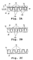
- a lower glass or plastic plate 28 can be provided with spaced-apart etched channels 14 . While each channel 14 is shown having vertical sidewalls 14 a and a flat bottom or floor region 14 b , which meet at ninety-degree angles, other channel geometries can be employed, as shown, for example, in FIG. 3 .
- the sidewalls 14 a of the channels can have bandpass characteristics that substantially only permit passage of the excitation (laser) beam 48 through the device.
- a coating material 52 can be applied to the channel sidewalls 14 a and, optionally, the floor regions 14 b (see FIG. 2A ); micro-optical elements 54 can be attached on each sidewall 14 a (see FIG. 2B ); the whole lower etched plate, including the channels in their entireties, can be coated with a bandpass coating 52 permitting only excitation light to pass through (see FIG. 2C ); or a combination thereof.
- An upper or cover plate 26 can be provided with bandpass characteristics that allow only sample emission (for example, fluorescence) wavelengths to pass through, and can prevent the passage of excitation beam wavelengths.
- a bandpass coating material 56 as shown in FIG. 2A , can be applied to one or more face regions of the upper plate 26 that face the lower plate 28 and channels 14 , at least along regions along the detection zone.
- a micro-optical bandpass element 55 as shown in FIG. 2B can be attached to the face of upper plate 26 confronting lower plate.
- Optical elements and coatings useful in connection with the present teachings are described, for example, in U.S. Pat. Nos., 3,466,120; 6,112,005; 5,872,655; 4,663,557; 6,100,541; each of which is incorporated herein in its entirety by reference.
- bandpass characteristics permitting passage of the excitation laser beam 48 through the device, and preventing the passage of excitation beam wavelengths between channels can be achieved by dyeing, doping, impregnating, mixing, compositing, or coating the material of the channel sidewalls 14 a , and/or the material of the channel bottom or floor region 14 b , with a light-absorbing and/or light-quenching material, for example, with a non-fluorescent quencher (NFQ).
- NFQ non-fluorescent quencher
- the term “light-absorbing and/or light-quenching material” is meant to include any dye, pigment, colorant, or other radiatively absorptive material that is capable of absorbing one or more ranges of wavelengths.
- the light-absorbing and/or light-quenching material can allow a first range of wavelengths to pass through.
- the use of one or more NFQ in the channel sidewalls and/or bottom can help to prevent or eliminate optical cross-talk between the channels.
- One or more NFQ can be incorporated into material of the sidewalls and/or bottom of the channel, or can be coated thereon.
- the channel material can be coated with an NFQ dye-containing photoresist.
- the coated material can be exposed to light, while the remaining material can be protected, for example, by a mask.
- the photoresist can then be developed, retaining the light-exposed portions of the coating on the channel material.
- the coated portions of the channel material can optionally be coated with a conformal coating, for example, an acrylic, a urethane, an epoxy, a silicone, or a poly-para-xylylene, for example, Parylene, coating.
- the light-absorbing and/or light-quenching coated portions of the channel material can be coated with Parylene.
- the NFQ coating can be present on one or more portion of one or more sidewall, bottom region, or ceiling, of one or more channels.
- One or more portions of a channel or all of a channel can be coated.
- at least a portion of a channel within the detection zone and/or excitation beam pathway can be coated.
- the coating can be of any suitable thickness, for example, from about 0.01 mil to about 20 mils, or from about 0.1 mil to about 10 mils thick.
- the coating can be from about 2 mils to about 5 mils thick.
- the light-absorbing and/or light-quenching material can be incorporated into the substrate and/or cover material.
- one or more NFQ can be mixed with a substrate material while the material is in powdered, beaded, liquid, molten, or unreacted or uncured form.
- the concentration of the NFQ can be from about 0.01 percent to about 20 percent of the total volume of the mixture of the NFQ and the substrate material.
- the concentration of the NFQ can be from about 1 percent to about 5 percent.
- the NFQ-containing material can then be formed into a substrate, or a portion of a substrate, such as a substrate bottom, a sidewall, or a cover.
- the bottom and/or sidewall can be attached to remaining portions of the substrate by any method known in the art, for example, by use of an adhesive, or a hot-melt adhesive, or by thermal bonding, chemical bonding, heat fusion, or the like.
- the light-absorbing and/or light-quenching material can form all or a portion of a bottom, sidewall, or cover of one or more channels. More than one light-absorbing and/or light-quenching material, or more than one light-absorbing and/or light-quenching material, or more than one NFQ, can be used in a single substrate material.
- the light-absorbing and/or light-quenching material can be injected into the substrate after the substrate has been formed.
- one or more NFQs can be injected into alternating capillaries in a capillary array.
- one or more NFQs can be injected or placed into alternating channels in a channel array.
- one or more NFQs can be injected or placed into alternating wells in a plate of wells or vials.
- the NFQ can be mixed with an aqueous solution, a gel, or a polymer prior to injection or placement.
- one or more NFQs can be mixed with a pre-polymerized monomer solution, the mixture can be injected into alternating capillaries, and the mixture can be polymerized. The mixture can be polymerized prior to injection into alternating capillaries.
- one or more NFQs can be mixed with an aqueous solution and placed in alternating wells or vials in a plate or holder.
- the concentration of the NFQ can be from about 1 percent to about 50 percent of the total volume of the mixture of NFQ and the carrier solution.
- the concentration of the NFQ can be from about 10 percent to about 50 percent.
- an NFQ dye can be used as the light-absorbing and/or light-quenching material.
- the NFQ dye can be selected for use based on the reporter used in the sample. Where one or more reporter is used in a sample, one or more corresponding NFQ dye can be used to coat, or can be used in the material of, one or more portions of a corresponding channel for the sample. The portion or portions can include one or more portions of a sidewall of the channel, a bottom region of the channel, a ceiling of the channel, or a combination thereof.
- the one or more NFQ dye can pass light of the excitation frequency, or can pass light of the emission frequency, of one or more reporter, and can prevent passage of at least a substantial portion of one or more other wavelengths of light.
- suitable NFQs for blocking the emission wavelength of FAM from regions between channels can include Methyl Orange, Disperse Red 13, Basic Violet 14, Basic Red 9, and other non-fluorescent dyes having an absorbance with a ⁇ -max at about 520 nm.
- suitable NFQs for blocking the emission wavelength of ROX between channels can include Malachite Green, Ethyl Violet, Fast Green FCF, Brilliant Green, Crystal Violet, and other dyes known to those skilled in the art to absorb with a ⁇ -max at about 605 nm.
- an NFQ dye capable of substantially absorbing wavelengths at about the ⁇ -max of one or more of the reporters can be used.
- Crystal Violet can be used as the NFQ because it substantially absorbs light at both 520 nm and 605 nm.
- the ⁇ -max can vary or can be adjusted in response to or to compensate for the substance or substrate that the light travels through.
- excitation light can be permitted to pass laterally through the device in a side-entry, on-channel configuration while substantially excluding light of other bandwidths.
- Fluorescent emissions from sample zones can be permitted to pass out of the channel to a detector while substantially excluding light of other bandwidths.
- a number of commercial entities produce a wide range of coating technology products that can find use with the teachings herein, including bandpass filters, beamsplitters, reflectors, collectors, and sputtered metals.
- Such entities include, for example, Seoul Precision Optics Co., Korea; GM Vacuum Coating Laboratory, California, a division of Navitar Coating Labs; Optical Coating Laboratory, Inc., California a JDS Aniphase Company; and Guernsey Coating Laboratories Inc., California.
- an excitation beam of light can be directed toward the array from each lateral side of the device.
- two lasers can be employed, one on each side of the device.
- a single laser source 34 can be employed in combination with appropriate beam splitting 60 a and directing optics, for example, mirrors 60 b–e , so that light enters the array from each lateral side of the device.
- less than all of the channels provided by the device can be used to conduct separations.
- the left- and right-endmost channels might not be loaded with samples, while the remaining channels are so loaded, or every other channel might be utilized, with the intervening channels remaining unused.
- Other sample loading configurations as known to those skilled in the art, are also envisioned.
Abstract
Description
Claims (41)
Priority Applications (1)
| Application Number | Priority Date | Filing Date | Title |
|---|---|---|---|
| US10/623,913 US7019831B2 (en) | 2001-08-24 | 2003-07-21 | Separation device substrate including non-fluorescent quencher dye |
Applications Claiming Priority (3)
| Application Number | Priority Date | Filing Date | Title |
|---|---|---|---|
| US09/938,767 US6627433B2 (en) | 2001-08-24 | 2001-08-24 | Multi-channel analyte-separation device employing side-entry excitation |
| US10/455,986 US7381315B2 (en) | 2001-08-24 | 2003-06-07 | Multi-channel analyte-separation device employing side-entry excitation |
| US10/623,913 US7019831B2 (en) | 2001-08-24 | 2003-07-21 | Separation device substrate including non-fluorescent quencher dye |
Related Parent Applications (1)
| Application Number | Title | Priority Date | Filing Date |
|---|---|---|---|
| US10/455,986 Continuation-In-Part US7381315B2 (en) | 2001-08-24 | 2003-06-07 | Multi-channel analyte-separation device employing side-entry excitation |
Publications (2)
| Publication Number | Publication Date |
|---|---|
| US20040053404A1 US20040053404A1 (en) | 2004-03-18 |
| US7019831B2 true US7019831B2 (en) | 2006-03-28 |
Family
ID=31998228
Family Applications (1)
| Application Number | Title | Priority Date | Filing Date |
|---|---|---|---|
| US10/623,913 Expired - Fee Related US7019831B2 (en) | 2001-08-24 | 2003-07-21 | Separation device substrate including non-fluorescent quencher dye |
Country Status (1)
| Country | Link |
|---|---|
| US (1) | US7019831B2 (en) |
Cited By (7)
| Publication number | Priority date | Publication date | Assignee | Title |
|---|---|---|---|---|
| US20080219890A1 (en) * | 2005-08-04 | 2008-09-11 | Helicos Biosciences Corporation | Sample loading and recovery |
| US20080219888A1 (en) * | 2005-08-04 | 2008-09-11 | Helicos Biosciences Corporation | Multi-Channel Flow Cells |
| US20100196207A1 (en) * | 2009-02-02 | 2010-08-05 | David Steinmiller | Structures for controlling light interaction with microfluidic devices |
| US20110315902A1 (en) * | 2009-03-07 | 2011-12-29 | Wei Wu | Analyzer and method for sensing using the same |
| US20160266091A1 (en) * | 2008-03-21 | 2016-09-15 | Abbott Point Of Care, Inc. | Method and apparatus for analyzing individual cells or particulates using fluorescent quenching and/or bleaching |
| US10672503B2 (en) | 2012-03-05 | 2020-06-02 | Opko Diagnostics, Llc | Methods and apparatuses for conducting analyses |
| US10775369B2 (en) | 2007-05-04 | 2020-09-15 | Opko Diagnostics, Llc | Fluidic systems for analyses |
Families Citing this family (3)
| Publication number | Priority date | Publication date | Assignee | Title |
|---|---|---|---|---|
| EP2005141A2 (en) * | 2006-04-11 | 2008-12-24 | Guava Technologies, Inc. | Asymmetric capillary for capillary-flow cytometers |
| JP4676975B2 (en) * | 2007-09-13 | 2011-04-27 | シャープ株式会社 | Bi-directional optical transmission device |
| FR2966930B1 (en) * | 2010-10-28 | 2013-05-10 | Centre Nat Rech Scient | USE OF SIC PARTICLES FOR THE REVELATION OF PROTEINS AND NUCLEIC ACIDS |
Citations (26)
| Publication number | Priority date | Publication date | Assignee | Title |
|---|---|---|---|---|
| US4832815A (en) | 1987-10-30 | 1989-05-23 | Hitachi, Ltd. | Wavelength dispersion electrophoresis apparatus |
| US5114551A (en) | 1991-09-30 | 1992-05-19 | Bio-Rad Laboratories, Inc. | Multi-point detection method for electrophoresis and chromatography in capillaries |
| US5192412A (en) | 1990-11-30 | 1993-03-09 | Hitachi, Ltd. | Electrophoretic apparatus having arrayed electrophoresis lanes |
| US5268080A (en) | 1991-02-28 | 1993-12-07 | Hitachi, Ltd. | DNA detector and DNA detection method |
| US5277780A (en) | 1991-09-13 | 1994-01-11 | Hitachi, Ltd. | Electrophoresis gel migration apparatus |
| US5439578A (en) | 1993-06-03 | 1995-08-08 | The Governors Of The University Of Alberta | Multiple capillary biochemical analyzer |
| US5498324A (en) * | 1993-02-05 | 1996-03-12 | Iowa State University Research Foundation, Inc. | Multiplexed fluorescence detector system for capillary electrophoresis |
| US5529679A (en) | 1992-02-28 | 1996-06-25 | Hitachi, Ltd. | DNA detector and DNA detection method |
| US5552028A (en) | 1993-12-17 | 1996-09-03 | The Perkin-Elmer Corporation | Polymers for separation of biomolecules by capillary electrophoresis |
| US5582705A (en) | 1995-05-19 | 1996-12-10 | Iowa State University Research Foundation, Inc. | Multiplexed capillary electrophoresis system |
| EP0840115A2 (en) | 1996-11-05 | 1998-05-06 | Hitachi Electronics Engineering Co., Ltd. | DNA base sequencer |
| US5790727A (en) | 1997-02-05 | 1998-08-04 | Brookhaven Science Associates Llc | Laser illumination of multiple capillaries that form a waveguide |
| US5833827A (en) | 1995-09-29 | 1998-11-10 | Hitachi, Ltd. | Capillary array electrophoresis system |
| US5867266A (en) | 1996-04-17 | 1999-02-02 | Cornell Research Foundation, Inc. | Multiple optical channels for chemical analysis |
| US5910287A (en) * | 1997-06-03 | 1999-06-08 | Aurora Biosciences Corporation | Low background multi-well plates with greater than 864 wells for fluorescence measurements of biological and biochemical samples |
| US6017434A (en) * | 1995-05-09 | 2000-01-25 | Curagen Corporation | Apparatus and method for the generation, separation, detection, and recognition of biopolymer fragments |
| US6027695A (en) * | 1998-04-01 | 2000-02-22 | Dupont Pharmaceuticals Company | Apparatus for holding small volumes of liquids |
| US6159353A (en) | 1997-04-30 | 2000-12-12 | Orion Research, Inc. | Capillary electrophoretic separation system |
| US6171780B1 (en) * | 1997-06-02 | 2001-01-09 | Aurora Biosciences Corporation | Low fluorescence assay platforms and related methods for drug discovery |
| US6246046B1 (en) | 1999-01-21 | 2001-06-12 | University Of Pittsburgh | Method and apparatus for electronically controlled scanning of micro-area devices |
| US20020003091A1 (en) * | 2000-05-15 | 2002-01-10 | Masaya Kojima | Capillary array electrophoresis apparatus and method of separating and analyzing specimen |
| US6413782B1 (en) * | 1996-06-28 | 2002-07-02 | Caliper Technologies Corp. | Methods of manufacturing high-throughput screening systems |
| US20020176804A1 (en) * | 2000-10-06 | 2002-11-28 | Protasis Corporation | Microfluidic substrate assembly and method for making same |
| US20030190608A1 (en) * | 1999-11-12 | 2003-10-09 | Gary Blackburn | Microfluidic devices comprising biochannels |
| US20040026252A1 (en) * | 2000-07-21 | 2004-02-12 | Qingbo Li | Extended pathlength detection in separations |
| US6906797B1 (en) * | 1999-09-13 | 2005-06-14 | Aclara Biosciences, Inc. | Side light activated microfluid channels |
-
2003
- 2003-07-21 US US10/623,913 patent/US7019831B2/en not_active Expired - Fee Related
Patent Citations (30)
| Publication number | Priority date | Publication date | Assignee | Title |
|---|---|---|---|---|
| US4832815A (en) | 1987-10-30 | 1989-05-23 | Hitachi, Ltd. | Wavelength dispersion electrophoresis apparatus |
| US5192412A (en) | 1990-11-30 | 1993-03-09 | Hitachi, Ltd. | Electrophoretic apparatus having arrayed electrophoresis lanes |
| US5268080A (en) | 1991-02-28 | 1993-12-07 | Hitachi, Ltd. | DNA detector and DNA detection method |
| US5314602A (en) | 1991-02-28 | 1994-05-24 | Hitachi, Ltd. | DNA detector and DNA detection method |
| US5277780A (en) | 1991-09-13 | 1994-01-11 | Hitachi, Ltd. | Electrophoresis gel migration apparatus |
| US5114551A (en) | 1991-09-30 | 1992-05-19 | Bio-Rad Laboratories, Inc. | Multi-point detection method for electrophoresis and chromatography in capillaries |
| US5529679A (en) | 1992-02-28 | 1996-06-25 | Hitachi, Ltd. | DNA detector and DNA detection method |
| US5498324A (en) * | 1993-02-05 | 1996-03-12 | Iowa State University Research Foundation, Inc. | Multiplexed fluorescence detector system for capillary electrophoresis |
| US5439578A (en) | 1993-06-03 | 1995-08-08 | The Governors Of The University Of Alberta | Multiple capillary biochemical analyzer |
| US5552028A (en) | 1993-12-17 | 1996-09-03 | The Perkin-Elmer Corporation | Polymers for separation of biomolecules by capillary electrophoresis |
| US6236945B1 (en) | 1995-05-09 | 2001-05-22 | Curagen Corporation | Apparatus and method for the generation, separation, detection, and recognition of biopolymer fragments |
| US6017434A (en) * | 1995-05-09 | 2000-01-25 | Curagen Corporation | Apparatus and method for the generation, separation, detection, and recognition of biopolymer fragments |
| US5582705A (en) | 1995-05-19 | 1996-12-10 | Iowa State University Research Foundation, Inc. | Multiplexed capillary electrophoresis system |
| US5695626A (en) | 1995-05-19 | 1997-12-09 | Iowa State University Research Foundation | Capillaries for use in a multiplexed capillary electrophoresis system |
| US5741411A (en) | 1995-05-19 | 1998-04-21 | Iowa State University Research Foundation | Multiplexed capillary electrophoresis system |
| US5833827A (en) | 1995-09-29 | 1998-11-10 | Hitachi, Ltd. | Capillary array electrophoresis system |
| US5867266A (en) | 1996-04-17 | 1999-02-02 | Cornell Research Foundation, Inc. | Multiple optical channels for chemical analysis |
| US6413782B1 (en) * | 1996-06-28 | 2002-07-02 | Caliper Technologies Corp. | Methods of manufacturing high-throughput screening systems |
| EP0840115A2 (en) | 1996-11-05 | 1998-05-06 | Hitachi Electronics Engineering Co., Ltd. | DNA base sequencer |
| US5790727A (en) | 1997-02-05 | 1998-08-04 | Brookhaven Science Associates Llc | Laser illumination of multiple capillaries that form a waveguide |
| US6159353A (en) | 1997-04-30 | 2000-12-12 | Orion Research, Inc. | Capillary electrophoretic separation system |
| US6171780B1 (en) * | 1997-06-02 | 2001-01-09 | Aurora Biosciences Corporation | Low fluorescence assay platforms and related methods for drug discovery |
| US5910287A (en) * | 1997-06-03 | 1999-06-08 | Aurora Biosciences Corporation | Low background multi-well plates with greater than 864 wells for fluorescence measurements of biological and biochemical samples |
| US6027695A (en) * | 1998-04-01 | 2000-02-22 | Dupont Pharmaceuticals Company | Apparatus for holding small volumes of liquids |
| US6246046B1 (en) | 1999-01-21 | 2001-06-12 | University Of Pittsburgh | Method and apparatus for electronically controlled scanning of micro-area devices |
| US6906797B1 (en) * | 1999-09-13 | 2005-06-14 | Aclara Biosciences, Inc. | Side light activated microfluid channels |
| US20030190608A1 (en) * | 1999-11-12 | 2003-10-09 | Gary Blackburn | Microfluidic devices comprising biochannels |
| US20020003091A1 (en) * | 2000-05-15 | 2002-01-10 | Masaya Kojima | Capillary array electrophoresis apparatus and method of separating and analyzing specimen |
| US20040026252A1 (en) * | 2000-07-21 | 2004-02-12 | Qingbo Li | Extended pathlength detection in separations |
| US20020176804A1 (en) * | 2000-10-06 | 2002-11-28 | Protasis Corporation | Microfluidic substrate assembly and method for making same |
Non-Patent Citations (4)
| Title |
|---|
| Cheng et al., Development of a Multichannel Microfluidic Analysis System Employing Affinity Capillary Electrohoresis for Immunoassay, Anal. Chem., vol. 73, No. 7, pp. 1472-1479 (2001). |
| Huang et al., Acousto-Optical Deflection-Based Laser Beam Scanning for Fluorescence Detection on Mulitchannel Electrophoretic Microships, Anal. Chem., vol. 71, No. 23, pp. 5309-5314 (1999). |
| Tian et al. Capillary and Microchip Electrophoresis for Rapid Detection of Known Mutations by Combining Alle-Specific DNA Amplification with Heteroduplex Analysis, Clinical Chem., vol. 47, No. 2, pp. 173-185 (2001). |
| Wang et al., Microfabricated Electrophoresis Chips for Simultaneous Bioassays of Glucose, Uric Acid, Ascorbic Acid, and Acetaminophen, Anal. Chem., vol. 72, No. 11, pp. 2514-2518 (2000). |
Cited By (13)
| Publication number | Priority date | Publication date | Assignee | Title |
|---|---|---|---|---|
| US20080219888A1 (en) * | 2005-08-04 | 2008-09-11 | Helicos Biosciences Corporation | Multi-Channel Flow Cells |
| US20080219890A1 (en) * | 2005-08-04 | 2008-09-11 | Helicos Biosciences Corporation | Sample loading and recovery |
| US10775369B2 (en) | 2007-05-04 | 2020-09-15 | Opko Diagnostics, Llc | Fluidic systems for analyses |
| US20160266091A1 (en) * | 2008-03-21 | 2016-09-15 | Abbott Point Of Care, Inc. | Method and apparatus for analyzing individual cells or particulates using fluorescent quenching and/or bleaching |
| US9733233B2 (en) * | 2008-03-21 | 2017-08-15 | Abbott Point Of Care, Inc. | Method and apparatus for analyzing individual cells or particulates using fluorescent quenching and/or bleaching |
| US9827564B2 (en) | 2009-02-02 | 2017-11-28 | Opko Diagnostics, Llc | Fluidic systems and methods for analyses |
| US8221700B2 (en) * | 2009-02-02 | 2012-07-17 | Opko Diagnostics, Llc | Structures for controlling light interaction with microfluidic devices |
| US9770715B2 (en) | 2009-02-02 | 2017-09-26 | Opko Diagnostics, Llc | Structures for controlling light interaction with microfluidic devices |
| US9827563B2 (en) | 2009-02-02 | 2017-11-28 | Opko Diagnostics, Llc | Fluidic systems and methods for analyses |
| US20100196207A1 (en) * | 2009-02-02 | 2010-08-05 | David Steinmiller | Structures for controlling light interaction with microfluidic devices |
| US9068921B2 (en) * | 2009-03-07 | 2015-06-30 | Hewlett-Packard Development Company, L.P. | Analyzer and method for sensing using the same |
| US20110315902A1 (en) * | 2009-03-07 | 2011-12-29 | Wei Wu | Analyzer and method for sensing using the same |
| US10672503B2 (en) | 2012-03-05 | 2020-06-02 | Opko Diagnostics, Llc | Methods and apparatuses for conducting analyses |
Also Published As
| Publication number | Publication date |
|---|---|
| US20040053404A1 (en) | 2004-03-18 |
Similar Documents
| Publication | Publication Date | Title |
|---|---|---|
| US6627433B2 (en) | Multi-channel analyte-separation device employing side-entry excitation | |
| US6576108B1 (en) | DNA detector and DNA detection method | |
| US5730850A (en) | Capillary array electrophoresis system | |
| US9063007B2 (en) | Bioanalytical instrumentation using a light source subsystem | |
| US20170153203A1 (en) | Sequencing System with Memory | |
| Woolley et al. | Ultra-high-speed DNA fragment separations using microfabricated capillary array electrophoresis chips. | |
| US4908112A (en) | Silicon semiconductor wafer for analyzing micronic biological samples | |
| EP0723149A2 (en) | Capillary array electrophoresis system | |
| US7019831B2 (en) | Separation device substrate including non-fluorescent quencher dye | |
| US20060176481A1 (en) | End-column fluorescence detection for capillary array electrophoresis | |
| US20040163958A1 (en) | Straightflow system | |
| CA2445546A1 (en) | Multi-channel capillary electrophoresis device and method | |
| JPH09105738A (en) | Fluorescence detecting type capillary array electrophoretic device | |
| AU2002332634A1 (en) | Multi-channel analyte-separation device employing side-entry excitation | |
| JP3839412B2 (en) | Fluorescence detection type capillary array electrophoresis apparatus | |
| US6156177A (en) | DNA detector and DNA detection method | |
| JP3296351B2 (en) | Electrophoresis device | |
| JP3042487B2 (en) | Electrophoresis device | |
| JP3042370B2 (en) | Electrophoresis device | |
| JP2002257786A (en) | Electrophoretic device |
Legal Events
| Date | Code | Title | Description |
|---|---|---|---|
| AS | Assignment |
Owner name: APPLERA CORPORATION, CALIFORNIA Free format text: ASSIGNMENT OF ASSIGNORS INTEREST;ASSIGNORS:GROSSMAN, PAUL D.;FRAZIER, JEFFERY D.;HARDING, IAN;REEL/FRAME:014636/0811;SIGNING DATES FROM 20030822 TO 20030908 |
|
| CC | Certificate of correction | ||
| AS | Assignment |
Owner name: BANK OF AMERICA, N.A, AS COLLATERAL AGENT, WASHING Free format text: SECURITY AGREEMENT;ASSIGNOR:APPLIED BIOSYSTEMS, LLC;REEL/FRAME:021976/0001 Effective date: 20081121 Owner name: BANK OF AMERICA, N.A, AS COLLATERAL AGENT,WASHINGT Free format text: SECURITY AGREEMENT;ASSIGNOR:APPLIED BIOSYSTEMS, LLC;REEL/FRAME:021976/0001 Effective date: 20081121 |
|
| FPAY | Fee payment |
Year of fee payment: 4 |
|
| AS | Assignment |
Owner name: APPLIED BIOSYSTEMS INC.,CALIFORNIA Free format text: CHANGE OF NAME;ASSIGNOR:APPLERA CORPORATION;REEL/FRAME:023994/0538 Effective date: 20080701 Owner name: APPLIED BIOSYSTEMS, LLC,CALIFORNIA Free format text: MERGER;ASSIGNOR:APPLIED BIOSYSTEMS INC.;REEL/FRAME:023994/0587 Effective date: 20081121 Owner name: APPLIED BIOSYSTEMS INC., CALIFORNIA Free format text: CHANGE OF NAME;ASSIGNOR:APPLERA CORPORATION;REEL/FRAME:023994/0538 Effective date: 20080701 Owner name: APPLIED BIOSYSTEMS, LLC, CALIFORNIA Free format text: MERGER;ASSIGNOR:APPLIED BIOSYSTEMS INC.;REEL/FRAME:023994/0587 Effective date: 20081121 |
|
| FEPP | Fee payment procedure |
Free format text: PAYOR NUMBER ASSIGNED (ORIGINAL EVENT CODE: ASPN); ENTITY STATUS OF PATENT OWNER: LARGE ENTITY |
|
| AS | Assignment |
Owner name: APPLIED BIOSYSTEMS, INC., CALIFORNIA Free format text: LIEN RELEASE;ASSIGNOR:BANK OF AMERICA, N.A.;REEL/FRAME:030182/0677 Effective date: 20100528 |
|
| REMI | Maintenance fee reminder mailed | ||
| LAPS | Lapse for failure to pay maintenance fees | ||
| STCH | Information on status: patent discontinuation |
Free format text: PATENT EXPIRED DUE TO NONPAYMENT OF MAINTENANCE FEES UNDER 37 CFR 1.362 |
|
| FP | Lapsed due to failure to pay maintenance fee |
Effective date: 20140328 |
|
| AS | Assignment |
Owner name: APPLIED BIOSYSTEMS, LLC, CALIFORNIA Free format text: CORRECTIVE ASSIGNMENT TO CORRECT THE RECEIVING PARTY NAME PREVIOUSLY RECORDED AT REEL: 030182 FRAME: 0694. ASSIGNOR(S) HEREBY CONFIRMS THE RELEASE OF SECURITY INTEREST;ASSIGNOR:BANK OF AMERICA, N.A.;REEL/FRAME:038002/0001 Effective date: 20100528 Owner name: APPLIED BIOSYSTEMS, LLC, CALIFORNIA Free format text: CORRECTIVE ASSIGNMENT TO CORRECT THE RECEIVING PARTY NAME PREVIOUSLY RECORDED AT REEL: 030182 FRAME: 0677. ASSIGNOR(S) HEREBY CONFIRMS THE RELEASE OF SECURITY INTEREST;ASSIGNOR:BANK OF AMERICA, N.A.;REEL/FRAME:038002/0001 Effective date: 20100528 |