US7012668B2 - Method of measuring AC residual image in a liquid crystal display device - Google Patents
Method of measuring AC residual image in a liquid crystal display device Download PDFInfo
- Publication number
- US7012668B2 US7012668B2 US11/129,384 US12938405A US7012668B2 US 7012668 B2 US7012668 B2 US 7012668B2 US 12938405 A US12938405 A US 12938405A US 7012668 B2 US7012668 B2 US 7012668B2
- Authority
- US
- United States
- Prior art keywords
- bis
- liquid crystal
- residual image
- aminophenoxy
- film
- Prior art date
- Legal status (The legal status is an assumption and is not a legal conclusion. Google has not performed a legal analysis and makes no representation as to the accuracy of the status listed.)
- Expired - Fee Related
Links
Images


Classifications
-
- G—PHYSICS
- G02—OPTICS
- G02F—OPTICAL DEVICES OR ARRANGEMENTS FOR THE CONTROL OF LIGHT BY MODIFICATION OF THE OPTICAL PROPERTIES OF THE MEDIA OF THE ELEMENTS INVOLVED THEREIN; NON-LINEAR OPTICS; FREQUENCY-CHANGING OF LIGHT; OPTICAL LOGIC ELEMENTS; OPTICAL ANALOGUE/DIGITAL CONVERTERS
- G02F1/00—Devices or arrangements for the control of the intensity, colour, phase, polarisation or direction of light arriving from an independent light source, e.g. switching, gating or modulating; Non-linear optics
- G02F1/01—Devices or arrangements for the control of the intensity, colour, phase, polarisation or direction of light arriving from an independent light source, e.g. switching, gating or modulating; Non-linear optics for the control of the intensity, phase, polarisation or colour
- G02F1/13—Devices or arrangements for the control of the intensity, colour, phase, polarisation or direction of light arriving from an independent light source, e.g. switching, gating or modulating; Non-linear optics for the control of the intensity, phase, polarisation or colour based on liquid crystals, e.g. single liquid crystal display cells
- G02F1/133—Constructional arrangements; Operation of liquid crystal cells; Circuit arrangements
- G02F1/1333—Constructional arrangements; Manufacturing methods
- G02F1/1343—Electrodes
- G02F1/134309—Electrodes characterised by their geometrical arrangement
- G02F1/134363—Electrodes characterised by their geometrical arrangement for applying an electric field parallel to the substrate, i.e. in-plane switching [IPS]
-
- G—PHYSICS
- G02—OPTICS
- G02F—OPTICAL DEVICES OR ARRANGEMENTS FOR THE CONTROL OF LIGHT BY MODIFICATION OF THE OPTICAL PROPERTIES OF THE MEDIA OF THE ELEMENTS INVOLVED THEREIN; NON-LINEAR OPTICS; FREQUENCY-CHANGING OF LIGHT; OPTICAL LOGIC ELEMENTS; OPTICAL ANALOGUE/DIGITAL CONVERTERS
- G02F1/00—Devices or arrangements for the control of the intensity, colour, phase, polarisation or direction of light arriving from an independent light source, e.g. switching, gating or modulating; Non-linear optics
- G02F1/01—Devices or arrangements for the control of the intensity, colour, phase, polarisation or direction of light arriving from an independent light source, e.g. switching, gating or modulating; Non-linear optics for the control of the intensity, phase, polarisation or colour
- G02F1/13—Devices or arrangements for the control of the intensity, colour, phase, polarisation or direction of light arriving from an independent light source, e.g. switching, gating or modulating; Non-linear optics for the control of the intensity, phase, polarisation or colour based on liquid crystals, e.g. single liquid crystal display cells
- G02F1/133—Constructional arrangements; Operation of liquid crystal cells; Circuit arrangements
- G02F1/1333—Constructional arrangements; Manufacturing methods
- G02F1/1337—Surface-induced orientation of the liquid crystal molecules, e.g. by alignment layers
- G02F1/133711—Surface-induced orientation of the liquid crystal molecules, e.g. by alignment layers by organic films, e.g. polymeric films
- G02F1/133723—Polyimide, polyamide-imide
-
- G—PHYSICS
- G02—OPTICS
- G02F—OPTICAL DEVICES OR ARRANGEMENTS FOR THE CONTROL OF LIGHT BY MODIFICATION OF THE OPTICAL PROPERTIES OF THE MEDIA OF THE ELEMENTS INVOLVED THEREIN; NON-LINEAR OPTICS; FREQUENCY-CHANGING OF LIGHT; OPTICAL LOGIC ELEMENTS; OPTICAL ANALOGUE/DIGITAL CONVERTERS
- G02F1/00—Devices or arrangements for the control of the intensity, colour, phase, polarisation or direction of light arriving from an independent light source, e.g. switching, gating or modulating; Non-linear optics
- G02F1/01—Devices or arrangements for the control of the intensity, colour, phase, polarisation or direction of light arriving from an independent light source, e.g. switching, gating or modulating; Non-linear optics for the control of the intensity, phase, polarisation or colour
- G02F1/13—Devices or arrangements for the control of the intensity, colour, phase, polarisation or direction of light arriving from an independent light source, e.g. switching, gating or modulating; Non-linear optics for the control of the intensity, phase, polarisation or colour based on liquid crystals, e.g. single liquid crystal display cells
- G02F1/133—Constructional arrangements; Operation of liquid crystal cells; Circuit arrangements
- G02F1/1333—Constructional arrangements; Manufacturing methods
- G02F1/133345—Insulating layers
-
- G—PHYSICS
- G02—OPTICS
- G02F—OPTICAL DEVICES OR ARRANGEMENTS FOR THE CONTROL OF LIGHT BY MODIFICATION OF THE OPTICAL PROPERTIES OF THE MEDIA OF THE ELEMENTS INVOLVED THEREIN; NON-LINEAR OPTICS; FREQUENCY-CHANGING OF LIGHT; OPTICAL LOGIC ELEMENTS; OPTICAL ANALOGUE/DIGITAL CONVERTERS
- G02F1/00—Devices or arrangements for the control of the intensity, colour, phase, polarisation or direction of light arriving from an independent light source, e.g. switching, gating or modulating; Non-linear optics
- G02F1/01—Devices or arrangements for the control of the intensity, colour, phase, polarisation or direction of light arriving from an independent light source, e.g. switching, gating or modulating; Non-linear optics for the control of the intensity, phase, polarisation or colour
- G02F1/13—Devices or arrangements for the control of the intensity, colour, phase, polarisation or direction of light arriving from an independent light source, e.g. switching, gating or modulating; Non-linear optics for the control of the intensity, phase, polarisation or colour based on liquid crystals, e.g. single liquid crystal display cells
- G02F1/133—Constructional arrangements; Operation of liquid crystal cells; Circuit arrangements
- G02F1/1333—Constructional arrangements; Manufacturing methods
- G02F1/133337—Layers preventing ion diffusion, e.g. by ion absorption
-
- G—PHYSICS
- G02—OPTICS
- G02F—OPTICAL DEVICES OR ARRANGEMENTS FOR THE CONTROL OF LIGHT BY MODIFICATION OF THE OPTICAL PROPERTIES OF THE MEDIA OF THE ELEMENTS INVOLVED THEREIN; NON-LINEAR OPTICS; FREQUENCY-CHANGING OF LIGHT; OPTICAL LOGIC ELEMENTS; OPTICAL ANALOGUE/DIGITAL CONVERTERS
- G02F1/00—Devices or arrangements for the control of the intensity, colour, phase, polarisation or direction of light arriving from an independent light source, e.g. switching, gating or modulating; Non-linear optics
- G02F1/01—Devices or arrangements for the control of the intensity, colour, phase, polarisation or direction of light arriving from an independent light source, e.g. switching, gating or modulating; Non-linear optics for the control of the intensity, phase, polarisation or colour
- G02F1/13—Devices or arrangements for the control of the intensity, colour, phase, polarisation or direction of light arriving from an independent light source, e.g. switching, gating or modulating; Non-linear optics for the control of the intensity, phase, polarisation or colour based on liquid crystals, e.g. single liquid crystal display cells
- G02F1/133—Constructional arrangements; Operation of liquid crystal cells; Circuit arrangements
- G02F1/1333—Constructional arrangements; Manufacturing methods
- G02F1/1337—Surface-induced orientation of the liquid crystal molecules, e.g. by alignment layers
Definitions
- the present invention relates to a liquid crystal display device in which an electric field is applied in a direction approximately parallel to flat surfaces of substrates to drive a liquid crystal. It is particularly effective for application to a liquid crystal display device in which a residual image caused by pure AC driving is reduced, excellent display characteristics are provided and a productivity is excellent.
- a longitudinal electric field system typified by a twisted nematic display system in which an electrode driving a liquid crystal layer held between a pair of substrates is constructed of a transparent electrode formed opposite to each of the pair of substrates and an electric field provided in a direction approximately vertical to the surfaces of the substrates is applied to drive a liquid crystal was employed.
- a lateral electric field system in which an electric field applied to a liquid crystal is provided in a direction approximately parallel to surfaces of substrates was developed.
- this system the use of a pair of comb-like electrodes in which an electrode providing an electric field approximately in parallel with the surfaces of the electrodes is formed on one of the substrates is disclosed in, for example, Japanese Patent Publication No. 21,907/1988, U.S. Patent Specification No. 4,345,249, European Patent No. 91/10,936, Japanese Patent Laid-Open Nos. 222,397/1994 and 160,878/1994, and the like. It is unnecessary that the electrodes disclosed in these documents are transparent, and opaque metal electrodes having a high conductivity are used.
- Applicant of the present application has found, with respect to the foregoing liquid crystal display device of the lateral electric field system, that usual AC driving is conducted at a high temperature of 55 DEG C. or the like to form a residual image (this is referred to as an AC residual image) which leads to a display defect.
- Applicant of the application has made assiduous effort, and has consequently confirmed that it is not observed so long as the AC residual image is below a certain percentage. And, it has been found that for coping with the display defect caused by the display unevenness, it is effective to use a specific oriented film and increase an interaction between the oriented film and the liquid crystal molecules.
- the invention aims to provide a liquid crystal display device that enables high-quality image display upon eliminating the display defect caused by the AC residual image.
- the invention is characterized by the construction described in the following (1) to (6).
- a liquid crystal display device comprising a pair of substrates and a liquid crystal layer held between the pair of substrates, at least one of the pair of substrates being provided with plural electrodes for applying an electric field to the liquid crystal layer, a protecting film for protecting at least one of the plural electrodes and oriented films formed to cover the protecting film or the electrodes, in which the film thickness of the protecting film is in the range of from 0.1 mu m to 0.7 mu m, and an AC residual image of the oriented films is less than 8%.
- a specific resistance of the liquid crystal layer is 10 ⁇ 10> OMEGA .cm or more.
- At least one of the oriented films in (1) or (2) is an organic polymer containing at least one of a polymer and an oligomer in which a weight substance with a long-chain alkyl group applied to an amine component or an acid sentence is at least 5% and at most 30% of the total molar amount.
- a weight average molecular weight of the polymer and the oligomer in (3) is at least 2,000 and at most 30,000.
- the polymer and the oligomer in (3) or (4) contain a long-chain alkylene group of at least one of a main chain type and a terminal type.
- the oriented film in (1) to (5) is an organic polymer of a polymer and/or oligomer amic acid imide type, a polymer and/or oligomer amide-imide type, a polymer and/or oligomer imidosiloxane type or a polymer and/or oligomer amide-imide type containing a long-chain alkylene group.
- a liquid crystal display device comprising a pair of substrates and a liquid crystal layer held between the pair of substrates, at least one of the pair of substrates being provided with at least a pair of electrodes for applying an electric field to the liquid crystal layer, protecting films for protecting the plural electrodes and oriented films formed on the protecting films and the electrodes, in which the film thickness of the protecting films is less than 0.5 mu m, and an AC residual image of the oriented films is less than 8%.
- FIG. 1 is a schematic sectional view showing a simplified structure of one substrate, which describes a first working example of a liquid crystal display device according to the invention
- FIG. 2 is a schematic plan view showing a construction of various electrodes in a unit pixel, which describes the first working example of the liquid crystal display device according to the invention
- FIG. 3 is an equivalent circuit diagram describing a driving structure of the first working example of the liquid crystal display device according to the invention.
- FIG. 4 is a descriptive view of a rubbing angle and an angle of a deflection plate in the liquid crystal display device according to the invention.
- FIG. 5 is a block diagram of a measurement system for evaluating change in B-V characteristics
- FIG. 6 is a sectional view of an overlapped portion of a pixel electrode and a passivation film.
- FIG. 1 is a schematic sectional view showing a simplified structure of one substrate, which describes the first working example of the liquid crystal display device according to the invention.
- the substrate shown is a substrate on which electrodes are formed in a liquid crystal display device of a lateral electric field system.
- Element 1 is a common electrode, 2 a gate insulation film, 3 a pixel electrode, 4 a passivation film (insulation film), 5 an oriented film, 7 a glass substrate constituting a substrate on which electrodes are formed, 11 a thin film transistor, and 12 a picture signal electrode.
- FIG. 2 is a schematic plan view showing a construction of various electrodes in a unit pixel, which describes the first working example of the liquid crystal display device according to the invention.
- 9 is a scanning signal electrode, and 10 amorphous Si.
- the scanning signal electrode 9 and the common electrode 1 are formed on a glass substrate 7 polished, and the surfaces of the scanning signal electrode 9 and the common electrode 1 are coated with an alumina film which is an anode oxide film of aluminum Al.
- a gate insulation film 2 made of a silicon nitride SiN film and an amorphous silicon a-Si film 10 are formed to cover the scanning signal electrode 9 and the common electrode 1 , and the n-type a-Si film, the pixel electrode 3 and the picture signal electrode 12 are formed on this a-Si film 10 .
- a laminated electrode using chromium Cr in an undercoat layer and aluminum Al in an upper layer is used as the pixel electrode 3 and the picture signal electrode 12 .
- the film thickness is 0.2 mu m in total.
- the materials of the scanning signal electrode 9 , the common electrode 1 , the pixel electrode 3 and the picture signal electrode 12 are not limited to the foregoing materials, and they are not limited so long as they are metallic materials having a low electric resistance.
- a metal such as chromium, aluminum, copper, niobium or the like, an alloy such as CrMo, AlTiTa or the like, or a laminated structure using aluminum in an undercoat layer and chromium in an upper layer is also available.
- the pixel electrode 3 and the picture signal electrode 12 have, as shown in FIG. 2 , a structure that both are parallel to the striped common electrode 1 and intersect the scanning signal electrode 9 , and a transistor element (thin film transistor TFT) 11 and a metal electrode group are formed on one substrate.
- an electric field provided between the pixel electrode 3 and the common electrode 1 on one substrate is formed approximately in parallel with the surface of the substrate.
- the electrode arrangement is not limited to that shown in FIG. 2 .
- a structure for making the driving direction of the liquid crystal bidirectional in the pixel for example, a structure that the common electrode 1 and the pixel electrode 3 are in zigzag fashion or a structure that the common electrode 1 and the pixel electrode 3 are not parallel to the picture signal electrode 12 is also available.
- the number of pixels is 1,024( ⁇ 3) ⁇ 768, and the pixel pitch is 88 mu m in a lateral direction (namely, between common electrodes) and 264 mu m in a longitudinal direction (namely, between scanning signal electrodes).
- a substrate opposite to the substrate having the transistor element is provided thereon with a striped color filter of R, G and B three colors.
- a transparent resin for flattening a surface is laminated on this color filter.
- An epoxy resin is used as a material of the transparent resin.
- a polyimide-based oriented film is coated on the transparent resin.
- FIG. 3 is an equivalent circuit diagram describing a driving structure of the first working example of the liquid crystal display device according to the invention.
- Element 13 is a vertical scanning circuit, 14 a picture signal driving circuit, 15 a power supply circuit/controller, 17 a display section (liquid crystal panel), and 18 a common electrode driving circuit.
- Driving LSI is connected with the display section 17 , the vertical scanning circuit 13 and the picture signal driving circuit 14 are connected therewith, and a scanning signal voltage, a picture signal voltage, a timing signal and the like are supplied from the power supply circuit/controller 15 to conduct image display.
- FIG. 4 is a descriptive view of a rubbing angle and an angle of a deflection plate in the liquid crystal display device according to the invention.
- Element 6 is a direction of an electric field, 19 a rubbing direction, and 20 a transmission axis of the deflection plate.
- the rubbing directions 19 of the oriented films formed on the upper and lower substrates are approximately parallel to each other, and an angle fLC with the direction 6 of the electric field to be applied is 75 DEG.
- Two deflection plates (for example, G1220DU, trade name of a product made by Nitto Denko K.K.) are mounted above and below the liquid crystal panel.
- the deflected light transmission axis of one deflection plate is approximately parallel to the rubbing direction 19 , namely 75 DEG, and the deflected light transmission axis of another deflection plate is approximately orthogonal ( ⁇ 15 DEG) to the rubbing direction 19 . Normally close characteristics were thereby obtained.
- a liquid crystal containing a compound having three fluoro groups in its terminal as a main component and having a positive dielectric anisotropy DELTA epsilon is held between the substrates.
- SiN is used in the passivation film 4 , and its film thickness is in the range of from 0.1 to 0.7 mu m. That is, the present inventors have found that by reducing the film thickness of the passivation film, the flat region of the oriented film is increased as shown in FIG. 6 to reduce the AC residual image of the oriented film.
- FIG. 6( a ) is a sectional view of an overlapped portion of the pixel electrode 3 and the passivation film 4 when the film thickness of the passivation film 4 is great enough.
- FIG. 6( b ) is a sectional view of an overlapped portion of the pixel electrode 3 and the passivation film 4 when the film thickness of the passivation film 4 is in the range of from 0.1 to 0.7 mu m.
- the oriented film 5 is, as shown, flattened by X as compared with FIG. 6( a ).
- An orientation controlling force of the oriented film 5 is generated by so-called rubbing treatment.
- the flattening results in increasing the rubbed region and improving the orientation controlling force of the oriented film 5 .
- the AC residual image can be suppressed to conduct high-quality image display without display unevenness.
- the small film thickness of the oriented film 5 can decrease the intensity of the electric field applied to the interface of the oriented film. That is, by decreasing the intensity of the electric field applied to the interface of the oriented film, the AC residual image is suppressed.
- the film thickness of the passivation film 4 is less than 0.5 mu m.
- the film when the film is too thin, it cannot protect the pixel electrode 3 and the like.
- the AC residual image When it is thick, the AC residual image is not reduced. Thus, it has to be in the range of from 0.1 to 0.7 mu m.
- the AC residual image was less than 8% in case of the film thickness of 0.7 mu m, and the good image display was obtained.
- Plasma CVD was used in the formation of this passivation film 4 . This film formation took approximately 25 minutes.
- a polyimide oriented film made of 2,2-bis[4-(p-aminophenoxy)phenylpropane] and pyromellitic acid dihydrate is used as the oriented film 5 . Its film thickness is 50 nm.
- Specific examples include p-phenylenediamine, m-phenylenediamine, 4,4′-diaminoterphenyl, 4,4′-diaminodiphenylsulfone, 3,3′-diaminodiphenylsulfone, 4,4′-diaminodiphenyl benzoate, 4,4′-diaminodiphenylmethane, 2,2′-(4,4′-diaminodiphenyl)propane, 4,4′-bis(p-aminophenoxy)diphenylsulfone, 4,4′-bis(m-aminophenoxy)diphenylsulfone, 4,4′-bis(p-aminophenoxy)diphenyl ether, 4,4′-bis(p-aminophenoxy)diphenylketone, 4,4′-bis(P-aminophenoxy)diphenylmethane and 2,2′-[4,4′-bis(p-amin
- examples of a halogen group-free diamine copolymerizable with the foregoing include 4,4′-diaminodiphenyl ether-3-carbonamide, 3-3′diaminodiphenylsulfone, 3-3′dimethyl-4-4′diaminodiphenyl ether, 1,6-diaminohexane, 2-2′-bis[4-(4-aminophenoxy)diphenyl]propane, 2-2′-bis[4-(4-aminophenoxy)phenyl]methane, 2-2′-bis[4-(4-aminophenoxy)phenyl]sulfone, 2-2′-bis[4-(4-aminophenoxy)phenyl]ketone, 2-2′-bis[4-(4-aminophenoxy)phenyl]biphenyl, 2-2′-bis[4-(4-aminophenoxy)phenyl]cyclohexane, 2-2
- examples of the compound having the long-chain alkylene group as the acid component and other copolymerizable compounds can include octylsuccinic acid dianhydride, dodecylsuccinic acid dianhydride, octylmalonic acid dianhydride, decamethylenebistrimellitic acid dianhydride, decamethylenebistrimellitate dianhydride, 2,2-bis[4-(3,4-dicarboxyphenoxy)phenyl]octyltetracarboxylic acid dianhydride, 2,2-bis[4-(3,4-dicarboxybenzoyloxy)phenyl]tridecanetetracarboxylic acid dianhydride, 2,2-bis[4-(3,4-dicarboxyphenoxy)phenyl]tridecanetetracarboxylic acid dianhydride, stearic acid, stearyl chloride, pyromellitic acid dianhydride, methylpyromellitic acid dianhydride
- the formation of the oriented film can easily be conducted by not only a printing method but also a wet method such as a spin coating method, a bar coating method or the like.
- a wet method such as a spin coating method, a bar coating method or the like.
- the printing method, patterning or the like after the film formation is dispensed with and a productivity in particular can be improved.
- the presence or absence of the residual image formed by pure AC driving of the thus-formed liquid crystal display device can directly be judged by measuring whether or not the change in B-V characteristics (brightness-voltage characteristics) in the pure AC driving (change in initial brightness B and brightness B after retention for 30 minutes with half tone when white display is conducted and retained for 30 minutes to give the maximum brightness display in the usual driving and brightness-voltage characteristics are likewise measured) occurs. That is, when the B-V characteristics are changed, the B-V characteristics after display are different in two zones in which different displays are conducted respectively, and there is a difference in the B-V characteristics even when the same voltage is inputted, with the result that the difference in brightness occurs in the two zones and this is observed as a residual image.
- FIG. 5 is a block diagram of a measurement system for evaluating change in B-V characteristics.
- Numeral 21 is a thermostat, 22 a monitoring window (glass window), 23 a digital multimeter, 24 a measurement controller, 25 a sample (liquid crystal display device), 26 a back light, 27 a common voltage power supply, 28 a signal voltage supply, and 29 a gate voltage power supply.
- the liquid crystal display device 25 as the sample is measured after the temperature is stabilized for 4 or more hours along with the back light 26 .
- the liquid crystal panel 25 is subjected to pure AC driving (AC driving) with a DC component being 0 at a common voltage of 0 V.
- a gate of the liquid crystal display device 25 is subjected to DC driving, and 16 V is inputted into the gate.
- the common voltage was a fixed value of 0 V.
- An output from a brightness system is inputted into the measurement controller 24 by the digital multimeter as a brightness value.
- Vsig Brightness Bb
- Vsig Brightness Ba
- DELTA B (Vsig) before and after the pure AC driving “(1)” DELTA B (Vsig)(%) [Ba(Vsig) ⁇ Bb(Vsig)]/Bb(Vsig) can be obtained.
- the oriented film is easily formed more uniformly throughout the surface to further improve coverage of electrodes. Further, when the passivation film is thin to a certain extent, the crack becomes large, and the coating property in the crack is easily improved by a method such as UV/ozone irradiation or the like to further improve coverage by the oriented film.
- Liquid crystal display devices were produced in the same manner as in Example 1 except for the following items, and were evaluated. That is, the film thickness of the oriented film is 0.3 mu m, and the time required for formation of the passivation film is approximately 15 minutes.
- [H] pattern was displayed for 30 minutes, and then subjected to black display. At this time, the residual image was visually observed at 0 to 40 DEG C. and 55 DEG C. The results are shown in [Table 2].
- a liquid crystal display device was produced in the same manner as in (Example 1) except for the following matters, and was evaluated.
- the thus-formed display device was measured in the same manner as mentioned above. Consequently, the AC residual image is more than 12%, and the residual image remains.
- a liquid crystal display device was produced in the same manner as in (Example 1) except for the following matters.
- the use of the polyimide oriented film free from the side chain-type structure can suppress the AC residual image in the liquid crystal display device comprising a pair of substrates and a liquid crystal layer held between the pair of substrates, at least one of the pair of substrates being provided with plural electrodes for applying an electric field approximately parallel to the surface of the substrate to the liquid crystal layer, a protecting film formed for protecting at least one of the plural electrodes and oriented films formed on the protecting film or the electrodes, and can provide the high-quality image display without display unevenness.
Abstract
Description

(wherein X represents a direct bond, —O—, —CH2-, —SO2-, —CO—, —CO2- or —CONH—), or compounds having structures represented by the following general [formulas 2]

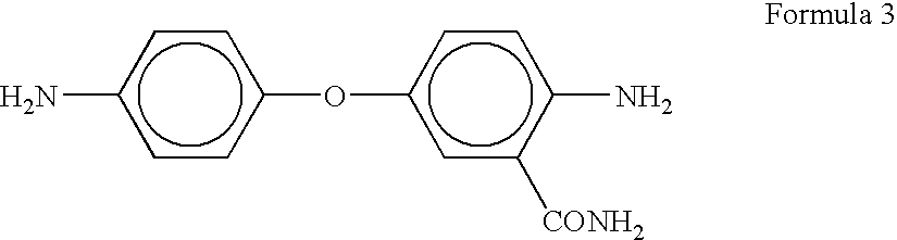
(wherein X is a direct bond), such as a bis(aminophenoxy)diphenyl compound and the like are used.
and diaminosiloxane compounds of the following [formulas 4].

| TABLE 1 | |||||
| Weight average | AC residual | ||||
| Diamine component | Acid component | molecular weight* | image** | ||
| Example 2 | 2,2′-bis[4-(4-aminophenoxy)phenyl] | octylsuccinic acid dianhydride | 12000 | <8% |
| biphenyl | ||||
| Example 3 | bis[2-(4-aminophenoxy)-5-cyclo | 2,2-bis[4-(3,4-dicarboxy-phenoxy) | 7290 | <8% |
| hexylphenyl]methane | phenyl]octyltetra-carboxylic | |||
| acid dianhydride | ||||
| Example 4 | 1,1-bis[2-(4-aminophenoxy)-3,5- | 3,3′,4,4′-biscyclohexane-tetracarboxylic | 3930 | <8% |
| dimethylphenyl]ethane | acid dianhydride | |||
| Example 5 | 2,2-bis[2-(4-aminophenoxy)phenyl] | 2,3,6,7-naphthalenetetra-carboxylic | 18530 | <8% |
| propane | acid dianhydride | |||
| Example 6 | 1,1-bis[2-(4-aminophenoxy)-5-methylphenyl] | 2,2-bis[4-(3,4-dicarboxy-phenoxy) | 19000 | <8% |
| butane | phenyl]propane-tetracarboxylic | |||
| acid dianhydride | ||||
| Example 7 | 1,1-bis[2-(4-aminophenoxy)-3,5- | 2,2-bis[4-(3,4-dicarboxy-benzoyloxy) | 27000 | <8% |
| dimethylphenyl]cyclohexane | phenyl]propane-tetracarboxylic | |||
| acid dianhydride | ||||
| Example 8 | 1.1-bis[2-(4-aminophenoxy)-5-methylphenyl]- | cyclopentanetetracarboxylic acid | 8510 | <8% |
| 3,3,5-trimethylcyclohexa | dianhydride | |||
| Example 9 | bis[4-(4-aminobenzoyl-oxy)benzoic | 1,2,3,4-cyclobutanetetra-carboxylic | 24180 | <8% |
| acid]propa | acid dianhydride | |||
| Example 10 | bis[2-(4-aminophenoxy)-5-n-propylphenyl] | 1,2,3,4-cyclopentanetetra-carboxylic | 22390 | <8% |
| methane | acid dianhydride | |||
| Comparative | m-phenylenediamine | 1,5bis[4-(3,4-dicarboxybenzoyloxy) | 4000 | 12% |
| Example 1 | phenyl]-decafluoropentanetetra- | |||
| carboxylic acid dianhydride + | ||||
| 1,2,3,4-butanetetra-carboxylic | ||||
| acid dianhydride | ||||
| TABLE 2 | |||
| AC | Use | Use | |
| residual | temperature | temperature | |
| image | 0 to 40° C. | 55° C. | |
| Examples 1 to 10 | <8% | ◯◯ | ◯◯ |
| Comparative Example 2 | 8 to 12% | ◯ | Δ |
| Comparative Example 1 | >12% | X | X |
| Visual observation: | |||
| ◯◯: No residual image is seen. | |||
| ◯: A residual image disappears within 3-minutes. | |||
| DELTA: A residual image disappears within 10 minutes. | |||
| X: A residual image is seen after 10 minutes. | |||
Claims (8)
ΔB (V sig) (%)=[B a (V sig)−B b (V sig)]/B b (Vsig).
ΔB (V sig) (%)=[B a (V sig)−B b (V sig)]/B b (V sig).
Priority Applications (1)
| Application Number | Priority Date | Filing Date | Title |
|---|---|---|---|
| US11/129,384 US7012668B2 (en) | 1999-01-22 | 2005-05-16 | Method of measuring AC residual image in a liquid crystal display device |
Applications Claiming Priority (3)
| Application Number | Priority Date | Filing Date | Title |
|---|---|---|---|
| PCT/JP1999/000244 WO2000043833A1 (en) | 1999-01-22 | 1999-01-22 | Liquid crystal display element |
| US88978801A | 2001-09-26 | 2001-09-26 | |
| US11/129,384 US7012668B2 (en) | 1999-01-22 | 2005-05-16 | Method of measuring AC residual image in a liquid crystal display device |
Related Parent Applications (2)
| Application Number | Title | Priority Date | Filing Date |
|---|---|---|---|
| PCT/JP1999/000244 Continuation WO2000043833A1 (en) | 1999-01-22 | 1999-01-22 | Liquid crystal display element |
| US88978801A Continuation | 1999-01-22 | 2001-09-26 |
Publications (2)
| Publication Number | Publication Date |
|---|---|
| US20050200795A1 US20050200795A1 (en) | 2005-09-15 |
| US7012668B2 true US7012668B2 (en) | 2006-03-14 |
Family
ID=14234773
Family Applications (1)
| Application Number | Title | Priority Date | Filing Date |
|---|---|---|---|
| US11/129,384 Expired - Fee Related US7012668B2 (en) | 1999-01-22 | 2005-05-16 | Method of measuring AC residual image in a liquid crystal display device |
Country Status (5)
| Country | Link |
|---|---|
| US (1) | US7012668B2 (en) |
| EP (1) | EP1156363A1 (en) |
| KR (1) | KR20020015023A (en) |
| CN (1) | CN1190693C (en) |
| WO (1) | WO2000043833A1 (en) |
Families Citing this family (2)
| Publication number | Priority date | Publication date | Assignee | Title |
|---|---|---|---|---|
| JP5016814B2 (en) * | 2005-12-14 | 2012-09-05 | 株式会社日立製作所 | Non-aqueous secondary battery |
| KR102648617B1 (en) * | 2016-06-30 | 2024-03-15 | 엘지디스플레이 주식회사 | Display device and the method for manufacturing the same |
Citations (9)
| Publication number | Priority date | Publication date | Assignee | Title |
|---|---|---|---|---|
| US5264953A (en) * | 1990-12-20 | 1993-11-23 | Asahi Glass Company Ltd. | Liquid crystal display apparatus for providing a gray scale and a projection type liquid crystal display apparatus |
| US5350539A (en) * | 1991-08-13 | 1994-09-27 | Nissan Chemical Industries Ltd. | Alignment treating agent for liquid crystal cell |
| US5600464A (en) * | 1993-09-20 | 1997-02-04 | Hitachi, Ltd. | Liquid crystal display device having the electric field parallel to the substrates |
| JPH1039306A (en) | 1996-07-29 | 1998-02-13 | Mitsubishi Electric Corp | Liquid crystal display device |
| US5831707A (en) * | 1994-08-24 | 1998-11-03 | Hitachi, Ltd. | Active matrix type liquid crystal display apparatus |
| US5933202A (en) * | 1995-09-28 | 1999-08-03 | Nec Corporation | Liquid crystal display device having an alternating common electrode voltage |
| US5936689A (en) * | 1997-03-14 | 1999-08-10 | Kabushiki Kaisha Toshiba | Liquid crystal display device |
| US6066696A (en) * | 1996-12-13 | 2000-05-23 | Samsung Display Devices Co. Ltd. | Optical alignment composition, alignment layer formed using the same and LCD having the alignment layer |
| US6590411B2 (en) * | 2000-10-23 | 2003-07-08 | Lg. Philips Lcd Co., Ltd. | Image sticking measurement method for liquid crystal display device |
Family Cites Families (4)
| Publication number | Priority date | Publication date | Assignee | Title |
|---|---|---|---|---|
| JPH05265006A (en) * | 1992-03-17 | 1993-10-15 | Sharp Corp | Production of oriented film for liquid crystal |
| JPH09230354A (en) * | 1996-02-21 | 1997-09-05 | Sagami Chem Res Center | Polyamide-based liquid crystal alignment layer treating agent |
| JP3613421B2 (en) * | 1996-05-31 | 2005-01-26 | Jsr株式会社 | Liquid crystal alignment agent |
| JPH10319382A (en) * | 1997-05-20 | 1998-12-04 | Nec Corp | Liquid crystal display device |
-
1999
- 1999-01-22 WO PCT/JP1999/000244 patent/WO2000043833A1/en not_active Application Discontinuation
- 1999-01-22 KR KR1020017009203A patent/KR20020015023A/en not_active Application Discontinuation
- 1999-01-22 EP EP99901143A patent/EP1156363A1/en not_active Withdrawn
- 1999-01-22 CN CNB998164119A patent/CN1190693C/en not_active Expired - Lifetime
-
2005
- 2005-05-16 US US11/129,384 patent/US7012668B2/en not_active Expired - Fee Related
Patent Citations (10)
| Publication number | Priority date | Publication date | Assignee | Title |
|---|---|---|---|---|
| US5264953A (en) * | 1990-12-20 | 1993-11-23 | Asahi Glass Company Ltd. | Liquid crystal display apparatus for providing a gray scale and a projection type liquid crystal display apparatus |
| US5350539A (en) * | 1991-08-13 | 1994-09-27 | Nissan Chemical Industries Ltd. | Alignment treating agent for liquid crystal cell |
| US5600464A (en) * | 1993-09-20 | 1997-02-04 | Hitachi, Ltd. | Liquid crystal display device having the electric field parallel to the substrates |
| US6300994B1 (en) * | 1993-09-20 | 2001-10-09 | Hitachi, Ltd. | Liquid crystal display device with substantial elimination of residual image |
| US5831707A (en) * | 1994-08-24 | 1998-11-03 | Hitachi, Ltd. | Active matrix type liquid crystal display apparatus |
| US5933202A (en) * | 1995-09-28 | 1999-08-03 | Nec Corporation | Liquid crystal display device having an alternating common electrode voltage |
| JPH1039306A (en) | 1996-07-29 | 1998-02-13 | Mitsubishi Electric Corp | Liquid crystal display device |
| US6066696A (en) * | 1996-12-13 | 2000-05-23 | Samsung Display Devices Co. Ltd. | Optical alignment composition, alignment layer formed using the same and LCD having the alignment layer |
| US5936689A (en) * | 1997-03-14 | 1999-08-10 | Kabushiki Kaisha Toshiba | Liquid crystal display device |
| US6590411B2 (en) * | 2000-10-23 | 2003-07-08 | Lg. Philips Lcd Co., Ltd. | Image sticking measurement method for liquid crystal display device |
Also Published As
| Publication number | Publication date |
|---|---|
| WO2000043833A1 (en) | 2000-07-27 |
| EP1156363A1 (en) | 2001-11-21 |
| KR20020015023A (en) | 2002-02-27 |
| CN1190693C (en) | 2005-02-23 |
| CN1338064A (en) | 2002-02-27 |
| US20050200795A1 (en) | 2005-09-15 |
Similar Documents
| Publication | Publication Date | Title |
|---|---|---|
| US11520186B2 (en) | Liquid crystal display and method for manufacturing same | |
| EP0806698B1 (en) | In-plane switching-mode active-matrix liquid crystal display | |
| US9494826B2 (en) | Liquid crystal display device and manufacturing method thereof | |
| JP5109371B2 (en) | Liquid crystal aligning agent for vertical alignment, liquid crystal alignment film, and liquid crystal display device using the same | |
| US7790248B2 (en) | Active matrix type liquid crystal display apparatus | |
| JP2743460B2 (en) | Liquid crystal cell alignment agent | |
| JPH1138415A (en) | Liquid crystal display element | |
| JP3740788B2 (en) | Active matrix liquid crystal display device | |
| US7012668B2 (en) | Method of measuring AC residual image in a liquid crystal display device | |
| JP3780082B2 (en) | Active matrix liquid crystal display device | |
| US7615260B2 (en) | Active-matrix liquid crystal display | |
| JPH10292113A (en) | Composition for liquid crystal alignment film | |
| JP3208980B2 (en) | Active matrix type liquid crystal display | |
| JP4186994B2 (en) | Active matrix liquid crystal display device | |
| JPH08146430A (en) | Liquid crystal display element | |
| JPH1010535A (en) | Flattening and orientation control film for liquid crystal | |
| JP2000105382A (en) | Liquid crystal display device | |
| JPH10319406A (en) | Active matrix type liquid crystal display device | |
| JPH086030A (en) | Composition for liquid crystal oriented film and liquid crystal oriented film | |
| JP2000302866A (en) | Liquid crystal oriented film composition, liquid crystal- holding base plate and liquid crystal display device | |
| JPH09160046A (en) | Composition for liquid crystal alignment layer | |
| JPH086031A (en) | Liquid crystal display element | |
| JP2002040436A (en) | Liquid crystal display device |
Legal Events
| Date | Code | Title | Description |
|---|---|---|---|
| FEPP | Fee payment procedure |
Free format text: PAYOR NUMBER ASSIGNED (ORIGINAL EVENT CODE: ASPN); ENTITY STATUS OF PATENT OWNER: LARGE ENTITY |
|
| FPAY | Fee payment |
Year of fee payment: 4 |
|
| AS | Assignment |
Owner name: HITACHI DISPLAYS, LTD., JAPAN Free format text: COMPANY SPLIT PLAN TRANSFERRING ONE HUNDRED (100) PERCENT SHARE OF PATENT AND PATENT APPLICATIONS;ASSIGNOR:HITACHI, LTD.;REEL/FRAME:027362/0612 Effective date: 20021001 Owner name: PANASONIC LIQUID CRYSTAL DISPLAY CO., LTD., JAPAN Free format text: MERGER/CHANGE OF NAME;ASSIGNOR:IPS ALPHA SUPPORT CO., LTD.;REEL/FRAME:027363/0315 Effective date: 20101001 Owner name: IPS ALPHA SUPPORT CO., LTD., JAPAN Free format text: COMPANY SPLIT PLAN TRANSFERRING FIFTY (50) PERCENT SHARE OF PATENTS AND PATENT APPLICATIONS;ASSIGNOR:HITACHI DISPLAYS, LTD.;REEL/FRAME:027362/0466 Effective date: 20100630 |
|
| FPAY | Fee payment |
Year of fee payment: 8 |
|
| FEPP | Fee payment procedure |
Free format text: MAINTENANCE FEE REMINDER MAILED (ORIGINAL EVENT CODE: REM.) |
|
| LAPS | Lapse for failure to pay maintenance fees |
Free format text: PATENT EXPIRED FOR FAILURE TO PAY MAINTENANCE FEES (ORIGINAL EVENT CODE: EXP.) |
|
| STCH | Information on status: patent discontinuation |
Free format text: PATENT EXPIRED DUE TO NONPAYMENT OF MAINTENANCE FEES UNDER 37 CFR 1.362 |
|
| FP | Lapsed due to failure to pay maintenance fee |
Effective date: 20180314 |