US7011734B2 - Method of manufacturing semiconductor device having silicide layer - Google Patents
Method of manufacturing semiconductor device having silicide layer Download PDFInfo
- Publication number
- US7011734B2 US7011734B2 US10/685,796 US68579603A US7011734B2 US 7011734 B2 US7011734 B2 US 7011734B2 US 68579603 A US68579603 A US 68579603A US 7011734 B2 US7011734 B2 US 7011734B2
- Authority
- US
- United States
- Prior art keywords
- temperature
- silicon substrate
- layer
- semiconductor device
- sputtering
- Prior art date
- Legal status (The legal status is an assumption and is not a legal conclusion. Google has not performed a legal analysis and makes no representation as to the accuracy of the status listed.)
- Expired - Lifetime, expires
Links
- 239000004065 semiconductor Substances 0.000 title claims abstract description 29
- 238000004519 manufacturing process Methods 0.000 title claims abstract description 25
- 229910021332 silicide Inorganic materials 0.000 title claims description 45
- FVBUAEGBCNSCDD-UHFFFAOYSA-N silicide(4-) Chemical compound [Si-4] FVBUAEGBCNSCDD-UHFFFAOYSA-N 0.000 title claims description 45
- 239000000758 substrate Substances 0.000 claims abstract description 99
- 238000004544 sputter deposition Methods 0.000 claims abstract description 94
- 229910052710 silicon Inorganic materials 0.000 claims abstract description 64
- 238000000137 annealing Methods 0.000 claims abstract description 58
- XUIMIQQOPSSXEZ-UHFFFAOYSA-N Silicon Chemical compound [Si] XUIMIQQOPSSXEZ-UHFFFAOYSA-N 0.000 claims abstract description 57
- 239000010703 silicon Substances 0.000 claims abstract description 57
- 238000010438 heat treatment Methods 0.000 claims abstract description 15
- 230000005540 biological transmission Effects 0.000 claims abstract description 6
- QVGXLLKOCUKJST-UHFFFAOYSA-N atomic oxygen Chemical compound [O] QVGXLLKOCUKJST-UHFFFAOYSA-N 0.000 claims abstract description 5
- 239000001301 oxygen Substances 0.000 claims abstract description 5
- 229910052760 oxygen Inorganic materials 0.000 claims abstract description 5
- 238000000034 method Methods 0.000 claims description 20
- 230000008569 process Effects 0.000 claims description 18
- ATJFFYVFTNAWJD-UHFFFAOYSA-N Tin Chemical compound [Sn] ATJFFYVFTNAWJD-UHFFFAOYSA-N 0.000 claims description 13
- 239000002131 composite material Substances 0.000 claims description 10
- 229910020711 Co—Si Inorganic materials 0.000 claims description 4
- 229910021420 polycrystalline silicon Inorganic materials 0.000 claims description 4
- 229920005591 polysilicon Polymers 0.000 claims description 3
- 125000006850 spacer group Chemical group 0.000 claims description 3
- 239000010410 layer Substances 0.000 description 97
- 239000012299 nitrogen atmosphere Substances 0.000 description 17
- 239000012535 impurity Substances 0.000 description 11
- 238000006243 chemical reaction Methods 0.000 description 9
- 239000002184 metal Substances 0.000 description 9
- 229910052751 metal Inorganic materials 0.000 description 9
- 238000009826 distribution Methods 0.000 description 8
- 238000002474 experimental method Methods 0.000 description 8
- 150000002500 ions Chemical class 0.000 description 8
- ZOXJGFHDIHLPTG-UHFFFAOYSA-N Boron Chemical compound [B] ZOXJGFHDIHLPTG-UHFFFAOYSA-N 0.000 description 7
- 229910052796 boron Inorganic materials 0.000 description 7
- 238000002955 isolation Methods 0.000 description 7
- 230000001186 cumulative effect Effects 0.000 description 6
- 230000004888 barrier function Effects 0.000 description 4
- 238000000151 deposition Methods 0.000 description 4
- 239000000203 mixture Substances 0.000 description 4
- 238000007796 conventional method Methods 0.000 description 3
- 238000011065 in-situ storage Methods 0.000 description 3
- -1 B ions Chemical class 0.000 description 2
- 229910019044 CoSix Inorganic materials 0.000 description 2
- MHAJPDPJQMAIIY-UHFFFAOYSA-N Hydrogen peroxide Chemical compound OO MHAJPDPJQMAIIY-UHFFFAOYSA-N 0.000 description 2
- VYPSYNLAJGMNEJ-UHFFFAOYSA-N Silicium dioxide Chemical compound O=[Si]=O VYPSYNLAJGMNEJ-UHFFFAOYSA-N 0.000 description 2
- QAOWNCQODCNURD-UHFFFAOYSA-N Sulfuric acid Chemical compound OS(O)(=O)=O QAOWNCQODCNURD-UHFFFAOYSA-N 0.000 description 2
- 230000004913 activation Effects 0.000 description 2
- 238000005229 chemical vapour deposition Methods 0.000 description 2
- 229910017052 cobalt Inorganic materials 0.000 description 2
- 239000010941 cobalt Substances 0.000 description 2
- GUTLYIVDDKVIGB-UHFFFAOYSA-N cobalt atom Chemical compound [Co] GUTLYIVDDKVIGB-UHFFFAOYSA-N 0.000 description 2
- 230000008021 deposition Effects 0.000 description 2
- 230000000694 effects Effects 0.000 description 2
- 238000005530 etching Methods 0.000 description 2
- 230000003993 interaction Effects 0.000 description 2
- 238000005259 measurement Methods 0.000 description 2
- 230000003647 oxidation Effects 0.000 description 2
- 238000007254 oxidation reaction Methods 0.000 description 2
- 238000001020 plasma etching Methods 0.000 description 2
- 229910052814 silicon oxide Inorganic materials 0.000 description 2
- 239000002344 surface layer Substances 0.000 description 2
- 230000003746 surface roughness Effects 0.000 description 2
- 229910052785 arsenic Inorganic materials 0.000 description 1
- 239000012298 atmosphere Substances 0.000 description 1
- 239000011810 insulating material Substances 0.000 description 1
- 239000000463 material Substances 0.000 description 1
- 238000012986 modification Methods 0.000 description 1
- 230000004048 modification Effects 0.000 description 1
- 229910052759 nickel Inorganic materials 0.000 description 1
- 229910052698 phosphorus Inorganic materials 0.000 description 1
- 238000000206 photolithography Methods 0.000 description 1
- 230000000087 stabilizing effect Effects 0.000 description 1
Images


Classifications
-
- H—ELECTRICITY
- H01—ELECTRIC ELEMENTS
- H01L—SEMICONDUCTOR DEVICES NOT COVERED BY CLASS H10
- H01L21/00—Processes or apparatus adapted for the manufacture or treatment of semiconductor or solid state devices or of parts thereof
- H01L21/02—Manufacture or treatment of semiconductor devices or of parts thereof
- H01L21/04—Manufacture or treatment of semiconductor devices or of parts thereof the devices having at least one potential-jump barrier or surface barrier, e.g. PN junction, depletion layer or carrier concentration layer
- H01L21/18—Manufacture or treatment of semiconductor devices or of parts thereof the devices having at least one potential-jump barrier or surface barrier, e.g. PN junction, depletion layer or carrier concentration layer the devices having semiconductor bodies comprising elements of Group IV of the Periodic System or AIIIBV compounds with or without impurities, e.g. doping materials
- H01L21/28—Manufacture of electrodes on semiconductor bodies using processes or apparatus not provided for in groups H01L21/20 - H01L21/268
- H01L21/283—Deposition of conductive or insulating materials for electrodes conducting electric current
- H01L21/285—Deposition of conductive or insulating materials for electrodes conducting electric current from a gas or vapour, e.g. condensation
- H01L21/28506—Deposition of conductive or insulating materials for electrodes conducting electric current from a gas or vapour, e.g. condensation of conductive layers
- H01L21/28512—Deposition of conductive or insulating materials for electrodes conducting electric current from a gas or vapour, e.g. condensation of conductive layers on semiconductor bodies comprising elements of Group IV of the Periodic System
- H01L21/28518—Deposition of conductive or insulating materials for electrodes conducting electric current from a gas or vapour, e.g. condensation of conductive layers on semiconductor bodies comprising elements of Group IV of the Periodic System the conductive layers comprising silicides
Definitions
- the present invention relates to a semiconductor device manufacturing method, and more particularly to a method of manufacturing a semiconductor device having a silicide layer on a silicon surface.
- An electric conductivity of a semiconductor device can be adjusted by doping impurities into semiconductor.
- the gate electrode and source/drain electrodes of a MOS transistor are desired to have a resistance as small as possible.
- a silicide layer is formed on a silicon layer.
- Metal capable of being silicidated, such as Ni and Co, is deposited on a silicon layer and heated to conduct a silicidation reaction. Since the silicidation reaction does not occur on an insulating layer, a silicide layer can be formed only on an underlying silicon surface. This process is called a salicidation (self-aligned silicidation) process.
- the silicidation process is divided into two stages. At the first stage, primary annealing is performed to form intermediate silicide, and at the second stage after unreacted metal is removed, a secondary silicidation process is performed to form silicide of a low resistivity.
- the surface of the metal layer is covered with a cap layer of TiN or the like having a small oxygen transmission performance to prevent oxidation of the metal layer capable of being silicidated.
- the primary annealing is performed at a temperature of 400° C. to 550° C.
- the secondary annealing is performed at a temperature of 750° C. to 900° C. (IEDM 95-449).
- a metal layer capable of being silicidated is formed by sputtering on a heated silicon substrate.
- a silicon substrate is maintained at 450° C. and a Co film is formed by sputtering and then in-situ annealing is performed in vacuum by maintaining the temperature at 450° C.
- Primary annealing is performed in a nitrogen atmosphere and an unreacted Co film is removed. Thereafter, secondary annealing is performed in a nitrogen atmosphere (IEDM 95-445).
- Japanese Patent Laid-open Publication No. HEI-11-111642 proposes to form a porous insulating layer such as a natural oxide film on a silicon substrate as a barrier layer and to sputter Co on the barrier layer at a high temperature of 450° C. After a Co film is formed by sputtering, in-situ annealing is performed to react the whole quantity of the deposited Co film with the silicon substrate. Thereafter, an unreacted Co layer and barrier layer are removed to perform primary annealing at 600° C. in a nitrogen atmosphere and secondary annealing is performed at 800° C. in a nitrogen atmosphere.
- a silicon substrate is heated to 400° C. without forming a barrier layer, and Co is sputtered at a low speed of 0.05 to 3 nm/sec to react the whole quantity of the sputtered Co with the substrate.
- primary annealing is performed at 600° C. and secondary annealing is performed at 800° C. in both embodiments described above, sputtering is performed after the sputtering chamber is once evacuated to a vacuum pressure of 10 ⁇ 9 torr.
- Japanese Patent Laid-open Publication No. HEI-11-233456 proposes to sputter material which contains Co, while heating a silicon substrate to a temperature of 300° C. to 500° C. and to perform primary annealing in a nitrogen atmosphere at a temperature of 450° C. to 650° C. After an unreacted Co is removed, secondary annealing is performed in a nitrogen atmosphere at a temperature of 700° C. to 900° C. There is no disclosure of a vacuum pressure.
- An object of this invention is to provide a semiconductor device manufacturing method including a silicidation process capable of providing excellent electric characteristics and controllability.
- Another object of this invention is to provide a semiconductor device manufacturing method including a silicidation process capable of providing excellent electric characteristics and shape stability without complicating manufacture facilities.
- a method of manufacturing a semiconductor device having the steps of: (a) evacuating a sputtering chamber to a pressure of 1.5 ⁇ 10 ⁇ 8 torr to 9 ⁇ 10 ⁇ 8 torr and heating a silicon substrate to a temperature of 330° C.
- a semiconductor device can be formed which has a silicide layer having excellent electric characteristics and shape controllability.
- a high performance semiconductor device can be manufactured without using special manufacture facilities.
- FIGS. 1A to 1E are SEM photographs showing the configuration of each Co film sputtered on a Si substrate.
- FIGS. 2A to 2C are cross sectional TEM photographs of each sample formed by forming a Co layer by sputtering at a different substrate temperature and forming a TiN layer on the Co layer by sputtering.
- FIGS. 3A and 3B are a graph showing the contact characteristics of each sample formed at a different secondary annealing temperature and a graph showing the impurity concentration distribution of each contact region.
- FIGS. 4A and 4B are graphs showing the leak current characteristics of each sample formed by forming a Co silicide layer on an n-type region in a p-well.
- FIG. 5 is a graph showing the leak current characteristics of each sample having a different film thickness.
- FIGS. 6A to 6D are SEM photographs showing the configuration of each substrate surface formed with a silicide layer.
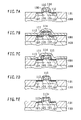
- FIGS. 7A to 7E are cross sectional views illustrating processes of forming a MOS transistor according to an embodiment of the invention.
- Co silicide is excellent in that it is not associated with the phenomenon that as the size becomes small, a resistivity per unit area increases as in the case of Ti silicide.
- Co silicide has the nature that its leak current is likely to increase as the size becomes small. The reason of leak current has been conventionally explained to be caused by spikes and the like. The present inventor made various experiments in order to discover a silicidation process capable of providing excellent electric characteristics and controllability.
- FIGS. 1A to 1E are photographs showing scanning electron microscope (SEM) surface observation images of each Co sputterred layer deposited on a Si substrate under different conditions.
- FIGS. 1A to 1C were obtained from each Co layer having a thickness of 30 nm formed through high temperature sputtering.
- the vacuum pressure in a sputtering chamber before sputtering was set to 2 ⁇ 10 ⁇ 7 torr and sputtering was performed at a substrate temperature of 450° C. It can be seen that the surface of the sputtered Co film is very rough.
- the Co layer having a thickness of 30 nm was formed by sputtering under the conditions that the vacuum pressure in a sputtering chamber before sputtering was set to 5 ⁇ 10 ⁇ 8 torr and sputtering was performed at a Si substrate temperature of 475° C.
- the surface roughness is considerably reduced.
- the surface is still rough in partial areas.
- the phenomenon that as the vacuum pressure is improved, the surface roughness is reduced, may be ascribed to some interaction of a deposited Co layer with foreign matters (impurities) attached to the substrate surface because of a poor vacuum pressure.
- the Co layer having a thickness of 30 nm was formed by sputtering under the conditions that the vacuum pressure in a sputtering chamber before sputtering was set to 5 ⁇ 10 ⁇ 8 torr and sputtering was performed at a slightly lowered Si substrate temperature of 450° C. It can be seen that the Co layer has an approximately uniform surface as a whole. It can be expected that the roughness of the film surface can be reduced by lowering the substrate temperature.
- the same conditions as those for the image shown in FIG. 1C were used, i.e., the conditions that the vacuum pressure in a sputtering chamber before sputtering was set to 5 ⁇ 10 ⁇ 8 torr and sputtering was performed at a Si substrate temperature of 450° C., excepting that a film thickness was reduced to 6 nm. It is generally difficult to maintain the surface flatness if the film is thinned. Almost a uniform surface is obtained even at a film thickness of 6 nm.
- the Co film having a thickness of 6 nm was formed under the same conditions as those for the image shown in FIG. 1D , excepting a slightly worsened vacuum pressure of 6 ⁇ 10 ⁇ 8 torr was used. Although the vacuum pressure is worsened from 5 ⁇ 10 ⁇ 8 torr to 6 ⁇ 10 ⁇ 8 torr, almost a uniform surface is obtained.
- FIGS. 2A to 2C are transmission electron microscope (TEM) observation images showing the configuration of each deposited film formed at a different Si substrate temperature during sputtering.
- TEM transmission electron microscope
- FIGS. 2A and 2B are photographs of samples obtained by depositing Co films having a thickness of 5 nm by sputtering and depositing a TiN film on the Co film at 150° C. under the conditions that a vacuum pressure before sputtering was set to 2 ⁇ 10 ⁇ 8 torr and the Si substrate temperatures were set to 355° C. and 280° C., respectively.
- a Co layer is not observed.
- Co sputtered at a substrate temperature of 355° C. reacts or is mixed with the Si substrate and becomes a CoSi x layer or a Co+Si mixed layer.
- the whole quantity of sputtered Co enters Si (or is mixed with a surface layer Si) to form a layer of a mixture of Co and Si.
- the TiN layer is formed on this layer.
- FIG. 2B shows an observation image when Co was deposited on a Si substrate at a temperature of 280° C. Similar to FIG. 2A , a layer of a mixture of Co and Si (CoSi x layer or Co+Si mixed layer) is formed on a Si substrate surface, and a Co layer is formed on this layer. It is considered that as the temperature becomes low, an interaction (reaction) between sputtered Co and the Si substrate becomes weak.
- the mixed layer of Co and Si is considered to be formed by the synergy achieved by a heated substrate and a sputtering energy. This layer is hereinafter called a composite layer.
- FIG. 2C is a TEM photograph showing a sample formed at a substrate temperature of 30° C. by forming a Co layer and a TiN layer in this order on the substrate at a vacuum pressure of 3 ⁇ 10 ⁇ 8 torr before sputtering.
- Co was sputtered at a substrate temperature of 30° C., the composite layer of Co and Si was not observed but a Co layer was formed on the Si substrate and a TiN layer was formed on the Co layer.
- FIGS. 3A and 3B are graphs showing the contact characteristics at a different Si substrate temperature during Co layer sputtering, and a secondary annealing temperature.
- Co film having a thickness of about 6 nm was formed by sputtering.
- a vacuum pressure before sputtering was 6 ⁇ 10 ⁇ 8 torr.
- Comparison samples were formed by sputtering without intentionally performing heating as in conventional techniques. Namely, Co sputtering was performed at a substrate temperature of 150° C., primary annealing was performed for 30 seconds at 500° C. in a nitrogen atmosphere, and secondary annealing was performed at 840° C.
- a Co layer was formed at a substrate temperature of 450° C. by sputtering, a TiN layer was formed covering the Co layer.
- primary annealing was performed for 30 seconds at 500° C. in a nitrogen atmosphere, secondary annealing was performed at 700° C. in a nitrogen atmosphere.
- FIG. 3A is the graph showing the resistance characteristics of samples.
- the abscissa represents a resistance value in an arbitrary scale, and the ordinate represents a cumulative probability in the unit of %.
- a probability curve p 1 As compared to a probability curve c 1 according to conventional techniques, a probability curve p 1 with high temperature sputtering and a lowered secondary annealing temperature shows a considerably lowered resistance value. In order to elucidate this reason, a boron (B) concentration was measured along a substrate depth direction.
- the graph shown in FIG. 3B shows a B concentration depth profile in samples.
- the abscissa represents a depth from a cobalt silicide surface in an arbitrary scale, and the ordinate represents a boron concentration in the unit of cm ⁇ 3 .
- An interface position between cobalt silicide and silicon is indicated by an arrow. It can be observed from the samples c 1 formed according to conventional techniques that the boron concentration lowers near at the interface with the silicide layer. For the samples p 1 with the high temperature sputtering and a lowered secondary annealing temperature, although the boron concentration near at the interface is not constant, it can be maintained fairly high as compared to the samples c 1 .
- a high contact resistance value of the samples c 1 may be ascribed to a lowered boron concentration of a silicon region in contact with the silicide.
- a low contact resistance of the samples p 1 may be ascribed to that the boron concentration of silicon in the interface region with the silicide is maintained high.
- the secondary annealing of the experiment was performed at 700° C.
- the good results can be expected by setting the secondary annealing temperature to 450° C. to 750° C.
- the secondary annealing temperature is more preferably set to 500° C. to 700° C.
- the primary annealing is generally performed for a primary silicidation reaction between metal and silicon, and is performed at a lower temperature than that of the secondary annealing.
- High temperature sputtering is considered to present the state that a silicide reaction starts already or that a silicide reaction is likely to occur.
- the primary annealing is required only to form intermediate silicide, along with the high temperature sputtering. It can be considered that the load of the primary annealing is reduced more than that with the low temperature sputtering.
- the primary annealing temperature may be lowered. An annealing time can be shortened assuming the same temperature.
- the primary annealing temperature may be set to 450° C. to 550° C.
- the primary annealing temperature is set lower than the secondary annealing temperature.
- a contact resistance can be lowered by raising the substrate temperature during sputtering and lowering the secondary annealing temperature. However, if the substrate temperature is raised during sputtering, it can be considered that the composite layer becomes the reason of leak current. Another problem is whether the reaction between sputtered metal and a silicon substrate is performed with good controllability.
- B ions are implanted into a Si substrate to form a p-type well.
- P ions are implanted in this p-well to form an n-type region.
- the surface of the substrate is cleaned.
- Each substrate is transported into a sputtering chamber and a Co film having a thickness of 5 nm is deposited by high temperature sputtering at a different substrate temperature and the same vacuum pressure of 2 ⁇ 10 ⁇ 8 torr before sputtering.
- a pure Co film is not formed but the composite film of Co and Si is formed.
- a Co film thickness of 5 nm is the thickness of the Co film on the insulating film.
- a TiN cap layer having a thickness of about 30 nm is formed.
- Primary annealing was performed for 30 seconds at 520° C. in a nitrogen atmosphere, and secondary annealing was performed for 30 seconds at 700° C. in a nitrogen atmosphere.
- the substrate temperatures during sputtering were set to 445° C. (# 7 ), 405° C. (# 8 ), 380° C. (# 9 ), 355° C. (# 10 ), 330° C. (# 11 ), and 280° C. (# 12 ), respectively. A junction leak current of each of these samples was measured.
- FIG. 4A is a graph showing a leak current and a cumulative count distribution.
- the abscissa represents a junction leak current in an arbitrary scale and the ordinate represents a cumulative count distribution according to the normal distribution. A rise of each sample has almost the same tendency. However, the sample # 12 obtained by the lowest Co sputtering temperature has the distribution that a leak current increases from a low cumulative count of about 30% to a high value of about two digits (orders of magnitude).
- the other samples show the good characteristics up to about 95%.
- the samples # 7 , # 8 and # 11 deteriorate their leak current by about one digit.
- the samples # 9 and # 10 maintain a good and low leak current up to about 99%.
- the leak current of the samples subjected to sputtering at the substrate temperature of 355° C. or 380° C. can be maintained at a very low level.
- the leak current of the samples subjected to sputtering at the substrate temperature of 330° C. to 445° C. is maintained generally at the good level.
- the samples subjected to sputtering at the lowest temperature of 280° C. have a considerably large leak current.
- the leak current can be maintained at a good level if the sputtering is performed at a substrate temperature of about 330° C. or higher.
- the substrate temperature during sputtering is more preferably set to 345° C. to 390° C. With this setting, a very low level of the leak current can be expected.
- the leak current of samples at the lowered substrate temperature of 30° C. during sputtering was also measured.
- the vacuum pressure before sputtering was set to 3 ⁇ 10 ⁇ 8 torr and the thicknesses of sputtered Co films at the substrate temperature of 30° C. were 5 nm (# 13 ) and 4.5 nm (# 13 - 1 ).
- a TiN film having a thickness of 30 nm was formed by sputtering.
- Primary annealing was performed for 30 seconds at 520° C. in a nitrogen atmosphere, and secondary annealing was performed for 30 seconds at 700° C. in a nitrogen atmosphere.
- FIG. 4B shows the leak current characteristics of the samples # 13 and # 13 - 1 .
- the abscissa represents a junction leak current in an arbitrary scale and the ordinate represents a cumulative count distribution. Both samples show gently inclined curves from the rise points, and leak currents are generated to a considerable degree in a broad range of possibly levels. From the viewpoint of reducing leak current, it is essential to heat the substrate during sputtering.
- the data shown in FIG. 4A were obtained by forming a Co film having a thickness of 5 nm by sputtering. The effects of other thicknesses were also checked. The leak current characteristics were checked by changing a Co layer thickness at the substrate temperature of 355° C. which presented the good measurement results shown in FIG. 4A .
- the vacuum pressure before sputtering was set to 2 ⁇ 10 ⁇ 8 torr, the primary annealing was performed in a nitrogen atmosphere at a temperature of 520° C. and the secondary annealing was performed in a nitrogen atmosphere at a temperature of 700° C.
- the thicknesses of sputtered Co layers on insulating films were 5 nm (# 10 ), 4 nm (# 10 - 1 ), 6 nm (# 10 - 2 ) and 7 nm (# 10 - 3 ).
- FIG. 5 shows the measurement results of leak current.
- the abscissa represents a junction leak current in an arbitrary scale and the ordinate represents a cumulative count distribution according to the normal distribution.
- the characteristics of the samples are quite similar and distribute concentratedly on the same line. Almost 99% of the samples have the leak current suppressed to very low values.
- a very low leak current can be realized by using the Co layer having a thickness of 4 nm to 7 nm. This result is also expected for the case that the Co layer thickness is further reduced.
- FIGS. 6A to 6D are photographs showing the shape of each silicide layer formed by sputtering at the temperatures of 445° C., 405° C., 380° C. and 355° C.
- a region surrounded by a broken line in FIGS. 6A and 6B corresponds to a silicon region, and both sides of the silicon region correspond to the insulating isolation region.
- silicide is not only formed on the silicon region but also extends up to the isolation region to a considerable width. Silicide climbs up to the isolation region and distributes in a range wider than the wiring layer. If the shape of the silicide layer is not controllable, there is a possibility that wiring lines are electrically short-circuited in an unexpected area. It is desired that the climb-up of silicide up to the isolation region is as little as possible.
- the area of silicide is limited only to the same region as the underlying silicon region and silicide is not formed on the surface of the isolation region to maintain the surface clean.
- the substrate temperature during sputtering is preferable lower than 400° C. or more preferably 395° C. or lower, in order to form the silicide layer only on the silicon surface without making silicide climb up to the insulating layer. It is expected that at the sputtering temperature of 390° C. or lower, the climb-up of silicide can be prevented almost completely.
- the temperature of a Si substrate during sputtering is preferably in a range from 330° C. to 395° C. and more preferably in a range from 345° C. to 390° C.
- Impurities and the like flying and reaching the substrate surface can be reduced if the vacuum pressure is low.
- a specific vacuum system is required to obtain a vacuum pressure of 10 ⁇ 9 torr and it takes a long evacuation time.
- Practically satisfactory results were obtained in the vacuum pressure range from 2 ⁇ 10 ⁇ 8 torr to 6 ⁇ 10 ⁇ 8 torr. Satisfactory results can be expected in the vacuum pressure range from 1.5 ⁇ 10 ⁇ 8 torr to 9 ⁇ 10 ⁇ 8 torr. It is preferable to set the vacuum pressure to 1.5 ⁇ 10 ⁇ 8 torr to 6 ⁇ 10 ⁇ 8 torr.
- FIGS. 7A to, 7 E are cross sectional views illustrating the main processes of manufacturing a semiconductor device basing upon the above-described experiment results.
- a shallow trench is formed in the surface layer of a silicon substrate 100 , insulating material such as silicon oxide is buried in this trench, and the surface thereof is planarized to form a shallow trench isolation (STI) 101 .
- Impurity ions e.g., B ions, are implanted into an active region defined by STI to form a p-type well 102 .
- a gate insulating film 103 having a predetermined thickness, e.g., about 3 nm, is formed through thermal oxidation for example.
- a polycrystalline silicon layer 104 is formed on the gate insulating film 103 .
- the polysilicon layer 104 is patterned by photolithography and etching to form an insulated gate electrode 104 .
- n-type impurity ions e.g., P or As ions
- a silicon oxide layer or the like is deposited on the substrate surface by chemical vapor deposition (CVD) or the like and anisotropic etching such as reactive ion etching (RIE) is preformed to form insulating side wall spacers 106 only on the side walls of the gate electrode.
- Impurity ions of n-type are again implanted to form high impurity concentration source/drain regions 107 .
- a silicide layer is to be formed on an exposed silicon surface by a salicide process.
- the silicon substrate 100 is heated to a temperature of 330° C. to 395° C., more preferably to a temperature of 345° C. to 390° C., e.g., to 355° C., and Co is deposited by sputtering.
- the deposited Co layer 111 is partially mixed with Si on the silicon layer to form a Co—Si composite layer 112 .
- a TiN layer 114 is deposited on the Co layer 111 at a substrate temperature of 150° C. to a thickness of 30 nm for example.
- the total quantity of Co can be consumed in a composite layer of Co—Si and the Co layer disappears, as shown in FIG. 7C .
- the Co layer 111 remains deposited only on the surface of the insulating film. In-situ annealing may be performed after sputtering to enhance the reaction and obtain the structure shown in FIG. 7C .
- primary annealing is performed at a temperature of 450° C. to 550° C.
- the atmosphere is a nitrogen atmosphere for example.
- a primary silicidation process occurs between Co and Si to form a primary silicidated layer 113 .
- the unreacted Co layer 111 along with the TiN layer 114 are removed by a mixture of sulfuric acid and hydrogen peroxide.
- the silicide layer 113 is left on the exposed silicon surface.
- the substrate is heated in a nitrogen atmosphere to a temperature of 450° C. to 750° C. or more preferably to a temperature of 500° C. to 700° C. to perform secondary annealing.
- the high resistance silicide layer 113 is changed to a low resistance silicide layer 113 x.
- the source/drain regions and gate electrode formed with the low resistance silicide layer are obtained in the manner described above.
- a p-channel MOS transistor can be formed by reversing the conductivity type in the processes shown in FIGS. 7A to 7E .
- a CMOS circuit can be formed by forming an n-channel MOS transistor and a p-channel MOS transistor. It will be apparent to those skilled in the art that other various modifications, improvements, combinations, and the like can be made.
Abstract
Description
Claims (15)
Applications Claiming Priority (2)
| Application Number | Priority Date | Filing Date | Title |
|---|---|---|---|
| JP2002303452A JP3921437B2 (en) | 2002-10-17 | 2002-10-17 | Manufacturing method of semiconductor device |
| JP2002-303452 | 2002-10-17 |
Publications (2)
| Publication Number | Publication Date |
|---|---|
| US20040092123A1 US20040092123A1 (en) | 2004-05-13 |
| US7011734B2 true US7011734B2 (en) | 2006-03-14 |
Family
ID=32211553
Family Applications (1)
| Application Number | Title | Priority Date | Filing Date |
|---|---|---|---|
| US10/685,796 Expired - Lifetime US7011734B2 (en) | 2002-10-17 | 2003-10-16 | Method of manufacturing semiconductor device having silicide layer |
Country Status (2)
| Country | Link |
|---|---|
| US (1) | US7011734B2 (en) |
| JP (1) | JP3921437B2 (en) |
Families Citing this family (4)
| Publication number | Priority date | Publication date | Assignee | Title |
|---|---|---|---|---|
| US7064025B1 (en) * | 2004-12-02 | 2006-06-20 | International Business Machines Corporation | Method for forming self-aligned dual salicide in CMOS technologies |
| JP2006165469A (en) | 2004-12-10 | 2006-06-22 | Fujitsu Ltd | Semiconductor apparatus and its manufacturing method |
| US7939440B2 (en) * | 2005-06-15 | 2011-05-10 | Spansion Llc | Junction leakage suppression in memory devices |
| US7485572B2 (en) * | 2006-09-25 | 2009-02-03 | International Business Machines Corporation | Method for improved formation of cobalt silicide contacts in semiconductor devices |
Citations (5)
| Publication number | Priority date | Publication date | Assignee | Title |
|---|---|---|---|---|
| US5874342A (en) * | 1997-07-09 | 1999-02-23 | Lsi Logic Corporation | Process for forming MOS device in integrated circuit structure using cobalt silicide contacts as implantation media |
| JPH11111642A (en) | 1997-10-07 | 1999-04-23 | Nec Corp | Manufacture of semiconductor device |
| JPH11233456A (en) | 1997-12-05 | 1999-08-27 | Texas Instr Inc <Ti> | Manufacturing method of electronic device |
| US20030029715A1 (en) * | 2001-07-25 | 2003-02-13 | Applied Materials, Inc. | An Apparatus For Annealing Substrates In Physical Vapor Deposition Systems |
| US6864143B1 (en) * | 2000-01-24 | 2005-03-08 | Taiwan Semiconductor Manufacturing Company, Ltd. | Eliminate bridging between gate and source/drain in cobalt salicidation |
-
2002
- 2002-10-17 JP JP2002303452A patent/JP3921437B2/en not_active Expired - Fee Related
-
2003
- 2003-10-16 US US10/685,796 patent/US7011734B2/en not_active Expired - Lifetime
Patent Citations (5)
| Publication number | Priority date | Publication date | Assignee | Title |
|---|---|---|---|---|
| US5874342A (en) * | 1997-07-09 | 1999-02-23 | Lsi Logic Corporation | Process for forming MOS device in integrated circuit structure using cobalt silicide contacts as implantation media |
| JPH11111642A (en) | 1997-10-07 | 1999-04-23 | Nec Corp | Manufacture of semiconductor device |
| JPH11233456A (en) | 1997-12-05 | 1999-08-27 | Texas Instr Inc <Ti> | Manufacturing method of electronic device |
| US6864143B1 (en) * | 2000-01-24 | 2005-03-08 | Taiwan Semiconductor Manufacturing Company, Ltd. | Eliminate bridging between gate and source/drain in cobalt salicidation |
| US20030029715A1 (en) * | 2001-07-25 | 2003-02-13 | Applied Materials, Inc. | An Apparatus For Annealing Substrates In Physical Vapor Deposition Systems |
Non-Patent Citations (4)
| Title |
|---|
| English translation of JP 11-111642. * |
| English translation of JP 11-233456. * |
| K. Goto et al.; IEDM 95-449, pp. 18.2.1 to 18.2.4, 1995. Discussed in the spec. |
| Ken Inoue et al.; IEDM 95-445, pp. 18.1.1 to 18.1.4, 1995. Discussed in the spec. |
Also Published As
| Publication number | Publication date |
|---|---|
| US20040092123A1 (en) | 2004-05-13 |
| JP2004140181A (en) | 2004-05-13 |
| JP3921437B2 (en) | 2007-05-30 |
Similar Documents
| Publication | Publication Date | Title |
|---|---|---|
| US5723893A (en) | Method for fabricating double silicide gate electrode structures on CMOS-field effect transistors | |
| US6410427B1 (en) | Metal silicidation methods and methods for using same | |
| JP3285934B2 (en) | Method for manufacturing semiconductor device | |
| US7129548B2 (en) | MOSFET structure with multiple self-aligned silicide contacts | |
| US5933741A (en) | Method of making titanium silicide source/drains and tungsten silicide gate electrodes for field effect transistors | |
| US20090127594A1 (en) | MOS TRANSISTORS HAVING NiPtSi CONTACT LAYERS AND METHODS FOR FABRICATING THE SAME | |
| US20080227283A1 (en) | SELF-ALIGNED METAL TO FORM CONTACTS TO Ge CONTAINING SUBSTRATES AND STRUCTURE FORMED THEREBY | |
| US7666786B2 (en) | Methods of fabricating semiconductor devices having a double metal salicide layer | |
| US6335254B1 (en) | Methods of forming transistors | |
| US8044470B2 (en) | Semiconductor device and method of fabricating the same | |
| US6440868B1 (en) | Metal gate with CVD amorphous silicon layer and silicide for CMOS devices and method of making with a replacement gate process | |
| US7060610B2 (en) | Method for forming contact in semiconductor device | |
| US20090075477A1 (en) | Method of manufacturing semiconductor device | |
| US6440867B1 (en) | Metal gate with PVD amorphous silicon and silicide for CMOS devices and method of making the same with a replacement gate process | |
| JPH0794731A (en) | Semiconductor device and its manufacturing method | |
| US6635938B1 (en) | Semiconductor device and manufacturing method thereof | |
| US6221760B1 (en) | Semiconductor device having a silicide structure | |
| US7011734B2 (en) | Method of manufacturing semiconductor device having silicide layer | |
| US20060115967A1 (en) | Methods of manufacturing a semiconductor device | |
| JPH1093077A (en) | Semiconductor device and manufacturing method thereof | |
| JP2004228351A (en) | Semiconductor device and its manufacturing method | |
| JPH11177084A (en) | Semiconductor device and its manufacture | |
| JP4048179B2 (en) | Manufacturing method of semiconductor device | |
| JP2003022984A (en) | Production method for semiconductor device | |
| JP4044428B2 (en) | Manufacturing method of semiconductor device |
Legal Events
| Date | Code | Title | Description |
|---|---|---|---|
| AS | Assignment |
Owner name: FUJITSU LIMITED, JAPAN Free format text: ASSIGNMENT OF ASSIGNORS INTEREST;ASSIGNOR:IKEDA, KAZUTO;REEL/FRAME:014617/0188 Effective date: 20030922 |
|
| FEPP | Fee payment procedure |
Free format text: PAYOR NUMBER ASSIGNED (ORIGINAL EVENT CODE: ASPN); ENTITY STATUS OF PATENT OWNER: LARGE ENTITY |
|
| STCF | Information on status: patent grant |
Free format text: PATENTED CASE |
|
| AS | Assignment |
Owner name: FUJITSU MICROELECTRONICS LIMITED, JAPAN Free format text: ASSIGNMENT OF ASSIGNORS INTEREST;ASSIGNOR:FUJITSU LIMITED;REEL/FRAME:021976/0089 Effective date: 20081104 Owner name: FUJITSU MICROELECTRONICS LIMITED,JAPAN Free format text: ASSIGNMENT OF ASSIGNORS INTEREST;ASSIGNOR:FUJITSU LIMITED;REEL/FRAME:021976/0089 Effective date: 20081104 |
|
| FPAY | Fee payment |
Year of fee payment: 4 |
|
| AS | Assignment |
Owner name: FUJITSU SEMICONDUCTOR LIMITED, JAPAN Free format text: CHANGE OF NAME;ASSIGNOR:FUJITSU MICROELECTRONICS LIMITED;REEL/FRAME:024651/0744 Effective date: 20100401 |
|
| FPAY | Fee payment |
Year of fee payment: 8 |
|
| AS | Assignment |
Owner name: FUJITSU SEMICONDUCTOR LIMITED, JAPAN Free format text: CHANGE OF ADDRESS;ASSIGNOR:FUJITSU SEMICONDUCTOR LIMITED;REEL/FRAME:041188/0401 Effective date: 20160909 |
|
| MAFP | Maintenance fee payment |
Free format text: PAYMENT OF MAINTENANCE FEE, 12TH YEAR, LARGE ENTITY (ORIGINAL EVENT CODE: M1553) Year of fee payment: 12 |