US7009233B2 - Semiconductor integrated circuit device including dummy patterns located to reduce dishing - Google Patents

Semiconductor integrated circuit device including dummy patterns located to reduce dishing Download PDF

Info

Publication number
US7009233B2
US7009233B2 US10/405,615 US40561503A US7009233B2 US 7009233 B2 US7009233 B2 US 7009233B2 US 40561503 A US40561503 A US 40561503A US 7009233 B2 US7009233 B2 US 7009233B2
Authority
US
United States
Prior art keywords
region
dummy
integrated circuit
circuit device
semiconductor integrated
Prior art date
Legal status (The legal status is an assumption and is not a legal conclusion. Google has not performed a legal analysis and makes no representation as to the accuracy of the status listed.)
Expired - Lifetime
Application number
US10/405,615
Other versions
US20030183860A1 (en
Inventor
Hiroyuki Uchiyama
Hiraku Chakihara
Teruhisa Ichise
Michimoto Kaminaga
Current Assignee (The listed assignees may be inaccurate. Google has not performed a legal analysis and makes no representation or warranty as to the accuracy of the list.)
Renesas Electronics Corp
Original Assignee
Renesas Technology Corp
Hitachi ULSI Systems Co Ltd
Priority date (The priority date is an assumption and is not a legal conclusion. Google has not performed a legal analysis and makes no representation as to the accuracy of the date listed.)
Filing date
Publication date
Priority to US10/405,615 priority Critical patent/US7009233B2/en
Application filed by Renesas Technology Corp, Hitachi ULSI Systems Co Ltd filed Critical Renesas Technology Corp
Publication of US20030183860A1 publication Critical patent/US20030183860A1/en
Assigned to RENESAS TECHNOLOGY CORP. reassignment RENESAS TECHNOLOGY CORP. ASSIGNMENT OF ASSIGNORS INTEREST (SEE DOCUMENT FOR DETAILS). Assignors: HITACHI, LTD.
Priority to US11/028,208 priority patent/US7112870B2/en
Application granted granted Critical
Publication of US7009233B2 publication Critical patent/US7009233B2/en
Assigned to RENESAS TECHNOLOGY CORP. reassignment RENESAS TECHNOLOGY CORP. ASSIGNMENT OF ASSIGNORS INTEREST (SEE DOCUMENT FOR DETAILS). Assignors: HITACHI ULSI SYSTEMS CO., LTD.
Priority to US11/410,949 priority patent/US7154164B2/en
Priority to US11/602,178 priority patent/US7327014B2/en
Priority to US11/948,626 priority patent/US7696608B2/en
Priority to US12/757,364 priority patent/US8183091B2/en
Assigned to RENESAS ELECTRONICS CORPORATION reassignment RENESAS ELECTRONICS CORPORATION MERGER (SEE DOCUMENT FOR DETAILS). Assignors: RENESAS TECHNOLOGY CORP.
Priority to US13/336,801 priority patent/US8558352B2/en
Priority to US13/467,075 priority patent/US8569107B2/en
Priority to US14/059,873 priority patent/US9059100B2/en
Priority to US14/739,818 priority patent/US9275956B2/en
Assigned to RENESAS ELECTRONICS CORPORATION reassignment RENESAS ELECTRONICS CORPORATION CHANGE OF ADDRESS Assignors: RENESAS ELECTRONICS CORPORATION
Anticipated expiration legal-status Critical
Expired - Lifetime legal-status Critical Current

Links

Images

Classifications

    • HELECTRICITY
    • H01ELECTRIC ELEMENTS
    • H01LSEMICONDUCTOR DEVICES NOT COVERED BY CLASS H10
    • H01L21/00Processes or apparatus adapted for the manufacture or treatment of semiconductor or solid state devices or of parts thereof
    • H01L21/02Manufacture or treatment of semiconductor devices or of parts thereof
    • H01L21/04Manufacture or treatment of semiconductor devices or of parts thereof the devices having at least one potential-jump barrier or surface barrier, e.g. PN junction, depletion layer or carrier concentration layer
    • H01L21/18Manufacture or treatment of semiconductor devices or of parts thereof the devices having at least one potential-jump barrier or surface barrier, e.g. PN junction, depletion layer or carrier concentration layer the devices having semiconductor bodies comprising elements of Group IV of the Periodic System or AIIIBV compounds with or without impurities, e.g. doping materials
    • H01L21/30Treatment of semiconductor bodies using processes or apparatus not provided for in groups H01L21/20 - H01L21/26
    • H01L21/302Treatment of semiconductor bodies using processes or apparatus not provided for in groups H01L21/20 - H01L21/26 to change their surface-physical characteristics or shape, e.g. etching, polishing, cutting
    • HELECTRICITY
    • H01ELECTRIC ELEMENTS
    • H01LSEMICONDUCTOR DEVICES NOT COVERED BY CLASS H10
    • H01L23/00Details of semiconductor or other solid state devices
    • H01L23/544Marks applied to semiconductor devices or parts, e.g. registration marks, alignment structures, wafer maps
    • GPHYSICS
    • G03PHOTOGRAPHY; CINEMATOGRAPHY; ANALOGOUS TECHNIQUES USING WAVES OTHER THAN OPTICAL WAVES; ELECTROGRAPHY; HOLOGRAPHY
    • G03FPHOTOMECHANICAL PRODUCTION OF TEXTURED OR PATTERNED SURFACES, e.g. FOR PRINTING, FOR PROCESSING OF SEMICONDUCTOR DEVICES; MATERIALS THEREFOR; ORIGINALS THEREFOR; APPARATUS SPECIALLY ADAPTED THEREFOR
    • G03F9/00Registration or positioning of originals, masks, frames, photographic sheets or textured or patterned surfaces, e.g. automatically
    • G03F9/70Registration or positioning of originals, masks, frames, photographic sheets or textured or patterned surfaces, e.g. automatically for microlithography
    • G03F9/7073Alignment marks and their environment
    • G03F9/7076Mark details, e.g. phase grating mark, temporary mark
    • HELECTRICITY
    • H01ELECTRIC ELEMENTS
    • H01LSEMICONDUCTOR DEVICES NOT COVERED BY CLASS H10
    • H01L21/00Processes or apparatus adapted for the manufacture or treatment of semiconductor or solid state devices or of parts thereof
    • H01L21/02Manufacture or treatment of semiconductor devices or of parts thereof
    • H01L21/04Manufacture or treatment of semiconductor devices or of parts thereof the devices having at least one potential-jump barrier or surface barrier, e.g. PN junction, depletion layer or carrier concentration layer
    • H01L21/18Manufacture or treatment of semiconductor devices or of parts thereof the devices having at least one potential-jump barrier or surface barrier, e.g. PN junction, depletion layer or carrier concentration layer the devices having semiconductor bodies comprising elements of Group IV of the Periodic System or AIIIBV compounds with or without impurities, e.g. doping materials
    • H01L21/30Treatment of semiconductor bodies using processes or apparatus not provided for in groups H01L21/20 - H01L21/26
    • H01L21/302Treatment of semiconductor bodies using processes or apparatus not provided for in groups H01L21/20 - H01L21/26 to change their surface-physical characteristics or shape, e.g. etching, polishing, cutting
    • H01L21/306Chemical or electrical treatment, e.g. electrolytic etching
    • H01L21/30625With simultaneous mechanical treatment, e.g. mechanico-chemical polishing
    • HELECTRICITY
    • H01ELECTRIC ELEMENTS
    • H01LSEMICONDUCTOR DEVICES NOT COVERED BY CLASS H10
    • H01L21/00Processes or apparatus adapted for the manufacture or treatment of semiconductor or solid state devices or of parts thereof
    • H01L21/02Manufacture or treatment of semiconductor devices or of parts thereof
    • H01L21/04Manufacture or treatment of semiconductor devices or of parts thereof the devices having at least one potential-jump barrier or surface barrier, e.g. PN junction, depletion layer or carrier concentration layer
    • H01L21/18Manufacture or treatment of semiconductor devices or of parts thereof the devices having at least one potential-jump barrier or surface barrier, e.g. PN junction, depletion layer or carrier concentration layer the devices having semiconductor bodies comprising elements of Group IV of the Periodic System or AIIIBV compounds with or without impurities, e.g. doping materials
    • H01L21/30Treatment of semiconductor bodies using processes or apparatus not provided for in groups H01L21/20 - H01L21/26
    • H01L21/31Treatment of semiconductor bodies using processes or apparatus not provided for in groups H01L21/20 - H01L21/26 to form insulating layers thereon, e.g. for masking or by using photolithographic techniques; After treatment of these layers; Selection of materials for these layers
    • H01L21/3105After-treatment
    • H01L21/31051Planarisation of the insulating layers
    • H01L21/31053Planarisation of the insulating layers involving a dielectric removal step
    • HELECTRICITY
    • H01ELECTRIC ELEMENTS
    • H01LSEMICONDUCTOR DEVICES NOT COVERED BY CLASS H10
    • H01L21/00Processes or apparatus adapted for the manufacture or treatment of semiconductor or solid state devices or of parts thereof
    • H01L21/70Manufacture or treatment of devices consisting of a plurality of solid state components formed in or on a common substrate or of parts thereof; Manufacture of integrated circuit devices or of parts thereof
    • H01L21/71Manufacture of specific parts of devices defined in group H01L21/70
    • H01L21/76Making of isolation regions between components
    • H01L21/762Dielectric regions, e.g. EPIC dielectric isolation, LOCOS; Trench refilling techniques, SOI technology, use of channel stoppers
    • H01L21/76224Dielectric regions, e.g. EPIC dielectric isolation, LOCOS; Trench refilling techniques, SOI technology, use of channel stoppers using trench refilling with dielectric materials
    • H01L21/76229Concurrent filling of a plurality of trenches having a different trench shape or dimension, e.g. rectangular and V-shaped trenches, wide and narrow trenches, shallow and deep trenches
    • HELECTRICITY
    • H01ELECTRIC ELEMENTS
    • H01LSEMICONDUCTOR DEVICES NOT COVERED BY CLASS H10
    • H01L21/00Processes or apparatus adapted for the manufacture or treatment of semiconductor or solid state devices or of parts thereof
    • H01L21/70Manufacture or treatment of devices consisting of a plurality of solid state components formed in or on a common substrate or of parts thereof; Manufacture of integrated circuit devices or of parts thereof
    • H01L21/71Manufacture of specific parts of devices defined in group H01L21/70
    • H01L21/768Applying interconnections to be used for carrying current between separate components within a device comprising conductors and dielectrics
    • H01L21/76801Applying interconnections to be used for carrying current between separate components within a device comprising conductors and dielectrics characterised by the formation and the after-treatment of the dielectrics, e.g. smoothing
    • H01L21/76819Smoothing of the dielectric
    • HELECTRICITY
    • H01ELECTRIC ELEMENTS
    • H01LSEMICONDUCTOR DEVICES NOT COVERED BY CLASS H10
    • H01L21/00Processes or apparatus adapted for the manufacture or treatment of semiconductor or solid state devices or of parts thereof
    • H01L21/70Manufacture or treatment of devices consisting of a plurality of solid state components formed in or on a common substrate or of parts thereof; Manufacture of integrated circuit devices or of parts thereof
    • H01L21/77Manufacture or treatment of devices consisting of a plurality of solid state components or integrated circuits formed in, or on, a common substrate
    • H01L21/78Manufacture or treatment of devices consisting of a plurality of solid state components or integrated circuits formed in, or on, a common substrate with subsequent division of the substrate into plural individual devices
    • HELECTRICITY
    • H01ELECTRIC ELEMENTS
    • H01LSEMICONDUCTOR DEVICES NOT COVERED BY CLASS H10
    • H01L22/00Testing or measuring during manufacture or treatment; Reliability measurements, i.e. testing of parts without further processing to modify the parts as such; Structural arrangements therefor
    • H01L22/30Structural arrangements specially adapted for testing or measuring during manufacture or treatment, or specially adapted for reliability measurements
    • H01L22/34Circuits for electrically characterising or monitoring manufacturing processes, e. g. whole test die, wafers filled with test structures, on-board-devices incorporated on each die, process control monitors or pad structures thereof, devices in scribe line
    • HELECTRICITY
    • H01ELECTRIC ELEMENTS
    • H01LSEMICONDUCTOR DEVICES NOT COVERED BY CLASS H10
    • H01L23/00Details of semiconductor or other solid state devices
    • H01L23/58Structural electrical arrangements for semiconductor devices not otherwise provided for, e.g. in combination with batteries
    • H01L23/585Structural electrical arrangements for semiconductor devices not otherwise provided for, e.g. in combination with batteries comprising conductive layers or plates or strips or rods or rings
    • HELECTRICITY
    • H01ELECTRIC ELEMENTS
    • H01LSEMICONDUCTOR DEVICES NOT COVERED BY CLASS H10
    • H01L27/00Devices consisting of a plurality of semiconductor or other solid-state components formed in or on a common substrate
    • H01L27/02Devices consisting of a plurality of semiconductor or other solid-state components formed in or on a common substrate including semiconductor components specially adapted for rectifying, oscillating, amplifying or switching and having at least one potential-jump barrier or surface barrier; including integrated passive circuit elements with at least one potential-jump barrier or surface barrier
    • H01L27/0203Particular design considerations for integrated circuits
    • H01L27/0207Geometrical layout of the components, e.g. computer aided design; custom LSI, semi-custom LSI, standard cell technique
    • HELECTRICITY
    • H01ELECTRIC ELEMENTS
    • H01LSEMICONDUCTOR DEVICES NOT COVERED BY CLASS H10
    • H01L29/00Semiconductor devices adapted for rectifying, amplifying, oscillating or switching, or capacitors or resistors with at least one potential-jump barrier or surface barrier, e.g. PN junction depletion layer or carrier concentration layer; Details of semiconductor bodies or of electrodes thereof  ; Multistep manufacturing processes therefor
    • H01L29/66Types of semiconductor device ; Multistep manufacturing processes therefor
    • H01L29/68Types of semiconductor device ; Multistep manufacturing processes therefor controllable by only the electric current supplied, or only the electric potential applied, to an electrode which does not carry the current to be rectified, amplified or switched
    • H01L29/76Unipolar devices, e.g. field effect transistors
    • H01L29/772Field effect transistors
    • H01L29/78Field effect transistors with field effect produced by an insulated gate
    • HELECTRICITY
    • H01ELECTRIC ELEMENTS
    • H01LSEMICONDUCTOR DEVICES NOT COVERED BY CLASS H10
    • H01L2223/00Details relating to semiconductor or other solid state devices covered by the group H01L23/00
    • H01L2223/544Marks applied to semiconductor devices or parts
    • H01L2223/54453Marks applied to semiconductor devices or parts for use prior to dicing
    • HELECTRICITY
    • H01ELECTRIC ELEMENTS
    • H01LSEMICONDUCTOR DEVICES NOT COVERED BY CLASS H10
    • H01L2924/00Indexing scheme for arrangements or methods for connecting or disconnecting semiconductor or solid-state bodies as covered by H01L24/00
    • H01L2924/0001Technical content checked by a classifier
    • H01L2924/0002Not covered by any one of groups H01L24/00, H01L24/00 and H01L2224/00

Definitions

  • This invention relates to a semiconductor integrated circuit device and to a process for manufacturing the same; and, in particular, the invention relates to a process which can effectively be applied to a semiconductor integrated circuit device comprising a step for flattening a surface using CMP (Chemical Mechanical Polishing).
  • CMP Chemical Mechanical Polishing
  • DRAM Dynamic Random Access Memory
  • demand has been increasing in recent years for finer detail and a higher degree of integration. Due to the demand for greater detail in semiconductor integrated circuit devices, laminated structures in multilayer interconnections are unavoidable, but if a multilayer structure is used, imperfections are formed on the surface of the upper layer reflecting the imperfections in the substrate. If photolithography is performed when imperfections are present on the surface, sufficient tolerance of focal depth cannot be obtained in the exposure step, and this leads to poor resolution. Therefore, the surface is flattened using CMP in order to improve the photolithography of components formed on the surface.
  • the CMP technique is used also to form isolation regions.
  • LOCOS Local Oxidation of Silicon
  • frequenT 1 y frequenT 1 y used in the past
  • a shallow groove is formed on la main surface of the semiconductor substrate; this groove is filled with a silicon oxide film; and the silicon oxide in the regions outside the groove are removed by CMP to form a shallow groove isolation.
  • the periphery of the isolation region is sharply defined, so the periphery can also be used effectively as an element part, so that it is easier to achieve finer detail.
  • a method has been proposed where a dummy pattern is disposed in regions where there are large patterns or where there is a wide pattern interval.
  • the pattern interval is decreased due to the dummy pattern, so that the aforesaid wide area (global) dishing or undulations are suppressed.
  • a technique is disclosed wherein a dummy pattern is disposed in a region with a wide pattern interval to improve the flatness of the surface of an insulating film which fills the pattern.
  • a target is formed for an exposure device (such as a stepper or the like) which is used in photolithography.
  • a dummy pattern cannot be disposed on the periphery of this target as it is necessary to recognize the pattern.
  • the area of the target is normally of the order of several ⁇ m or more. Therefore, if a dummy pattern is not disposed in this large (large area) pattern region, dishing occurs as described above. In the prior art, as this large area pattern was formed in a scribe region and not in a product region, this was not considered to be a problem.
  • the dishing in the scribe region also affects the product region, and since the tolerance of focal depth in the exposure step is becoming more critical due to the trend towards higher detail, the decreased flatness of the product region (in particular the periphery) is a matter of concern.
  • a semiconductor integrated circuit device comprises a semiconductor substrate having a semiconductor element formed on a main surface, a first pattern comprising a dummy pattern formed on the main surface or on one of the layers on the main surface, and a second pattern formed on an upper layer of the first pattern and comprising a pattern which serves as a target for optical pattern recognition, the pattern which serves as a target for optical pattern recognition being enclosed within the flat shape of the dummy pattern.
  • the dummy pattern is disposed underneath the pattern used for optical pattern recognition, so that a decrease of the overall flatness in this pattern region is suppressed.
  • the first pattern may contain another dummy pattern having a smaller area than the dummy pattern.
  • the dummy pattern and another dummy pattern may also be formed in a scribe region. Further, other dummy patterns may be formed in a product region and a scribe region.
  • the dummy pattern is formed with an area equal to or greater, than a pattern prohibition region on the periphery of the pattern used for optical pattern recognition. Therefore, a decrease in the recognition rate of optical pattern recognition of this pattern is prevented.
  • the first pattern has patterning dimensions of the same order as the design rule of the semiconductor elements and contains another dummy pattern having a smaller area than the dummy pattern, but the other dummy pattern is not disposed in the pattern prohibition region.
  • the flatness of these regions is improved, and by prohibiting provision of the small area dummy pattern in the vicinity of this pattern, a decrease in the recognition rate of the pattern used for optical pattern recognition is prevented.
  • the dummy pattern is formed in the scribe region of the semiconductor wafer, and the other dummy pattern is formed in the product region and scribe region of the semiconductor wafer.
  • the flatness of the scribe region, as well as that of the product region is improved, and the flatness in the vicinity of the boundary of the product region and scribe region is improved. This contributes to improvement of the product yield.
  • the semiconductor integrated circuit device comprises a semiconductor substrate having a semiconductor element formed on its main surface, a first pattern formed on the main surface or on one of the layers on the main surface, and a second pattern formed on an upper layer of the first pattern.
  • the first pattern comprises a first dummy pattern
  • the second pattern comprises a second dummy pattern having a pattern pitch and pattern width of identical design dimensions to those of the first dummy pattern
  • the second dummy pattern is formed over a space of the first dummy pattern in its flat position.
  • One of the side edges of the second dummy pattern is formed so as to overlap with the first dummy pattern in its flat surface position, or the first dummy pattern and second dummy pattern are offset by a distance of 1 ⁇ 2 pitch in its flat surface position.
  • dishing does occur in the pattern interval between first small area dummy patterns, but the second small area dummy pattern is formed in the upper layer of the part where this dishing occurs, so that overlapping with the dishing formed between the second small area patterns is prevented.
  • overlapping of dishing between upper and lower layers is suppressed, and flatness is improved.
  • the first pattern may further comprise another dummy pattern having a larger area than that of the first dummy pattern
  • the second pattern may further comprise a pattern used for optical pattern recognition
  • the pattern used for optical pattern recognition may be enclosed within the flat shape of the other dummy pattern.
  • the other dummy pattern is formed with an area equal to or greater than the area of the pattern prohibition region on the periphery of the pattern used for optical pattern recognition, and the first dummy pattern is not disposed in the pattern prohibition region.
  • the other dummy pattern may also be formed in the scribe region of the semiconductor wafer, and the first and second dummy patterns may also be formed in the product region and scribe region of the semiconductor wafer.
  • the first pattern may be an active region pattern formed on the main surface
  • the second pattern may be a pattern formed in the same layer as that of the gate electrode forming the semiconductor elements.
  • the method of manufacturing the semiconductor integrated circuit device of this invention comprises (a) a step of forming a first pattern comprising a dummy pattern on the main surface or on any component surface on the main surface of a semiconductor substrate, (b) a step of depositing an insulating film on the main surface on which the first pattern is formed or on a component patterned on the first pattern, and flattening the surface by polishing the insulating film, and (c) a step of forming a second pattern comprising a pattern used for optical pattern recognition on the upper layer of the flattened surface.
  • the pattern used for optical pattern recognition is enclosed within the flat shape of the dummy pattern.
  • a step may further be provided for detecting the pattern used for optical pattern recognition to perform alignment of the semiconductor substrate.
  • the method of manufacturing the semiconductor integrated circuit device of this invention further comprises (a) a step of forming a first pattern comprising a dummy pattern on the main surface or on any component surface on the main surface of the semiconductor substrate, (b) a step of forming a second pattern comprising a pattern used for optical pattern recognition on the upper layer of the first pattern, and (c) a step of detecting the pattern used for optical pattern recognition to perform alignment of the semiconductor substrate.
  • the pattern used for optical pattern recognition is enclosed within the flat shape of the dummy pattern.
  • the dummy pattern may be formed with an area equal to or greater than the pattern prohibition region on the periphery of the pattern used for optical pattern recognition.
  • the first pattern further comprises a first dummy pattern
  • the second pattern further comprises a second dummy pattern having a pattern pitch and pattern width identical to the design dimensions of the first dummy pattern, the second dummy pattern being formed over a space of the first dummy pattern in its flat surface position.
  • One of the side edges of the second dummy pattern is formed so as to overlap with the first dummy pattern, or the first dummy pattern and second dummy pattern are offset at a distance of 1 ⁇ 2 pitch in its flat surface position.
  • the dummy patterns may be formed in the scribe region of the semiconductor wafer, and the first and second dummy patterns may be formed in the product region and scribe region of the semiconductor wafer.
  • the component to which the first pattern is transferred is the semiconductor substrate, and the component to which the second pattern is transferred is the gate electrode.
  • the aforesaid semiconductor integrated circuit device can be manufactured by these semiconductor integrated circuit device manufacturing methods.
  • FIG. 1 is a plan view showing a silicon wafer used for manufacturing a semiconductor integrated circuit device according to one embodiment of this invention.
  • FIG. 2 is a plan view showing an enlargement of a chip part of a wafer according to this embodiment.
  • FIG. 3 is a plan view showing an end region of the chip comprising a scribe line.
  • FIG. 4 is a plan view showing an enlargement of a product region of the chip.
  • FIG. 5( a ) and FIG. 5( b ) are sectional views showing an example of a method of manufacturing the semiconductor integrated circuit device according to the embodiment as a sequence of processes.
  • FIG. 6( a ) and FIG. 6( b ) are sectional views showing an example of a method of manufacturing the semiconductor integrated circuit device according to the embodiment as a sequence of processes.
  • FIG. 7( a ) and FIG. 7( b ) are sectional views showing an example of a method of manufacturing the semiconductor integrated circuit device according to the embodiment as a sequence of processes.
  • FIG. 8( a ) and FIG. 8( b ) are sectional views showing an example of a method of manufacturing the semiconductor integrated circuit device according to the embodiment as a sequence of processes.
  • FIG. 9( a ) and FIG. 9( b ) are sectional views showing an example of a method of manufacturing the semiconductor integrated circuit device according to the embodiment as a sequence of processes.
  • FIG. 10( a ) and FIG. 10( b ) are sectional views showing an example of a method of manufacturing the semiconductor integrated circuit device according to the embodiment as a sequence of processes.
  • FIG. 11( a ) and FIG. 11( b ) are sectional views showing an example of a method of manufacturing the semiconductor integrated circuit device according to the embodiment as a sequence of processes.
  • FIG. 12( a ) and FIG. 12( b ) are sectional views showing an example of a method of manufacturing the semiconductor integrated circuit device according to the embodiment as a sequence of processes.
  • FIG. 13( a ) and FIG. 13( b ) are sectional views showing an example of a method of manufacturing the semiconductor integrated circuit device according to the embodiment as a sequence of processes.
  • FIG. 14( a ) and FIG. 14( b ) are sectional views showing an example of a method of manufacturing the semiconductor integrated circuit device according to the embodiment as a sequence of processes.
  • FIG. 15( a ) and FIG. 15( b ) are sectional views showing an example of a method of manufacturing the semiconductor integrated circuit device according to the embodiment as a sequence of processes.
  • FIG. 16( a ) and FIG. 16( b ) are sectional views showing an example of a method of manufacturing the semiconductor integrated circuit device according to the embodiment as a sequence of processes.
  • FIG. 17 is a plan view showing an example of a method of manufacturing the semiconductor integrated circuit device according to the embodiment as part of a sequence of processes.
  • FIG. 18 is an enlarged plan view of FIG. 17 .
  • FIG. 19( a ) and FIG. 19( b ) are sectional views showing an example of a method of manufacturing the semiconductor integrated circuit device according to the embodiment as a sequence of processes.
  • FIG. 20( a ) and FIG. 20( b ) are sectional views showing an example of a method of manufacturing the semiconductor integrated circuit device according to the embodiment as a sequence of processes.
  • FIG. 21( a ) and FIG. 21( b ) are sectional views showing an example of a method of manufacturing the semiconductor integrated circuit device according to the embodiment as a sequence of processes.
  • FIG. 22( a ) and FIG. 22( b ) are sectional views showing an example of a method of manufacturing the semiconductor integrated circuit device according to the embodiment as a sequence of processes.
  • FIG. 23( a ) and FIG. 23( b ) are sectional views showing an example of a method of manufacturing the semiconductor integrated circuit device according to the embodiment as a sequence of processes.
  • FIG. 24 is a plan view showing an example of a method of manufacturing the semiconductor integrated circuit device according to the embodiment as part of a sequence of processes.
  • FIG. 25 is an enlarged plan view showing another example of the semiconductor integrated circuit device according to the embodiment.
  • FIG. 26 is an enlarged plan view showing another example of the semiconductor integrated circuit device according to the embodiment.
  • FIG. 27 is an enlarged plan view showing yet another example of the semiconductor integrated circuit device according to the embodiment.
  • FIG. 28 is an enlarged plan view showing yet another example of the semiconductor integrated circuit device according to the embodiment.
  • FIG. 1 is a plan view showing a silicon wafer used for manufacturing a semiconductor integrated circuit device according to one embodiment of the invention.
  • a notch In is made in a single crystal silicon wafer 1 w and serves as a crystal plane index mark of the wafer 1 w .
  • a chip 1 c is formed on the wafer 1 w .
  • the chip 1 c is formed in the effective processing area of the wafer 1 w , and a chip region 1 g outside the effective processing area is not used.
  • FIG. 2 is a plan view showing an enlargement of the chip 1 c of the wafer 1 w .
  • the chip 1 c is scribed and divided by a scribe line SL. In the steps described hereafter, each step is performed in the state of the wafer 1 w , the chip 1 c being divided in the final step.
  • the typical DRAM chip 1 c is shown as an example. It may also be another product, for example a logic product, such as a CPU, a memory element, such as an SRAM (Static Random Access Memory), or a memory which can be erased in one step and be electrically rewritten (so-called EEPROM: Electrical Erasable Read Only Memory), or a system LSI where a logic circuit and memory element coexist on the same chip.
  • a memory cell array MA, direct peripheral circuit PCd and indirect peripheral circuit Pci are formed in the chip 1 c . DRAM memory cells are formed in the memory cell array MA.
  • the direct peripheral circuit PCd is formed on the periphery of the memory cells MA.
  • the indirect peripheral circuit Pci is formed in the center region of the chip 1 c.
  • FIG. 3 is a plan view showing an edge region of the chip 1 c comprising the region of the scribe line SL.
  • FIG. 3 shows the state where an isolation region is formed on a semiconductor substrate 1 (wafer 1 w , chip 1 c ).
  • the regions other than a scribe region SR are product regions PR.
  • a target pattern T 1 , large area dummy pattern DL and small area pattern Ds are formed simultaneously when the isolation region is formed in the scribe region SR.
  • a TEG (Test Equipment Group) element is also formed in the scribe region SR, but it is not shown in the drawings.
  • the target pattern T 1 is a pattern formed simultaneously in a step when an isolation region pattern is formed, and it is used for alignment in an exposure step when a gate electrode pattern, to be described later, is formed. Specifically, it is used as a target for position detection when mask alignment of a target electrode pattern is performed. In an exposure device, a mask is aligned with respect to the wafer by, for example, performing optical pattern recognition of the target, and a photoresist film is then exposed.
  • the large area dummy pattern DL and small area dummy pattern Ds are patterns which are simultaneously formed in the step when the isolation region pattern is formed.
  • a target pattern T 2 is formed simultaneously with the target electrode pattern on the large area dummy pattern DL.
  • the target pattern T 2 is used for alignment in the exposure step when the upper layer pattern, for example, an interconnection pattern or connecting hole pattern, is formed. Due to the provision of the large area pattern DL, dishing in the target pattern region is prevented, the recognition rate of the target pattern is improved, and fine patterning can advantageously be performed.
  • a dummy pattern was not provided on the periphery of the prior art target pattern, so that the surface flatness of the target pattern periphery was impaired; however, by providing the large area dummy pattern DL underneath the target pattern, the flatness is improved and the recognition rate of the target pattern is improved.
  • the large area dummy pattern DL is formed to be larger than the target pattern so as to enclose the target pattern. In other words, the large area dummy pattern DL is present underneath the target pattern region used for optical pattern recognition, so that dishing is prevented and the recognition rate of the target pattern is improved.
  • On the periphery of the target pattern there is a region where any kind of pattern is prohibited, thereby to prevent interference with target pattern recognition.
  • the large area dummy pattern DL has an area equal to or greater than this pattern prohibition region. Therefore, the large area dummy pattern DL is not recognized as a pattern by the exposure device, and the recognition rate of the target patterns T 1 , T 2 is not decreased.
  • the small area dummy pattern Ds is formed in the scribe region SR and the product region PR. In other words, it is formed over the whole surface of the wafer W.
  • the small area dummy pattern Ds is disposed in a region in which there is a wide interval between patterns functioning as elements. Since there is a wide interval between patterns functioning as elements, if the small area dummy pattern Ds were not disposed in this wide pattern interval, dishing would occur in the pattern interval. Since this dishing becomes larger in depth as the pattern interval becomes wider, the flatness is largely impaired. By disposing this small area dummy pattern Ds in this wide inter-pattern space, the flatness is improved.
  • the pattern size and inter-pattern space are formed with dimensions of approximately the same order as those of the pattern forming the elements, the pattern interval is narrow, and a small amount of dishing according to the narrow pattern interval occurs. In this situation, the depression amount can be much improved and the flatness can be improved compared with the case when the dummy pattern is not provided.
  • the pattern size of the small area dummy pattern Ds is of the same order as the element design rule, and a suitable value is selected with regard to the ease of photolithography and the effect on suppression of dishing.
  • the pattern size of the small area dummy pattern Ds may also be set to the order of 0.2 ⁇ m.
  • the pattern size of the small area dummy pattern Ds may be set to be of the order of 1 ⁇ m, and the inter-pattern space may be set to be of the order of 0.4 ⁇ m. It will of course be understood that other figures can be selected from the requirements of the photolithography step. However, if the pattern size and inter-pattern space are too large, dishing in the inter-pattern space becomes more marked, which is undesirable.
  • the width of the scribe region SR is approximately 100 ⁇ m.
  • active regions which form elements are formed apart from the aforesaid small area dummy pattern Ds in the product region PR.
  • an active region L 1 forming a channel region of a MISFET (Metal Insulator Semiconductor Field Effect Transistor), an active region L 2 for well feed and an active region L 3 for guard band feed are shown as examples. It will be understood that other active regions may also be formed.
  • the aforesaid small area dummy pattern Ds is formed between the patterns of the active regions L 1 , L 2 , L 3 .
  • the large area dummy pattern DL may also be formed in the product region PR.
  • FIG. 4 is a plan view showing an enlargement of a region comprising the active regions L 1 , L 2 of the product region PR.
  • Plural small area dummy patterns Ds are disposed between the patterns of the active regions L 1 , L 2 , as described above.
  • the pattern size d 1 of the small area dummy pattern Ds is approximately 1 ⁇ m
  • the pattern interval S 1 is approximately 0.4 ⁇ m.
  • the small Area dummy pattern Ds is formed by automatically generating patterns of the aforesaid size in a lattice (grid) with the pattern pitch (1.4 ⁇ m in the case of this embodiment). At each lattice point, the small area dummy pattern Ds is not generated in parts where the active regions L 1 , L 2 are present. Specifically, in a mask design device, a graphic computation is performed which expands patterns such as the active regions L 1 , L 2 . This expanded pattern region is a pattern prohibition region R 1 of the small area dummy pattern Ds.
  • the lattice within the pattern prohibition region R 1 is excluded from the graphic computation, and the small area dummy pat@ern Ds is generated at the remaining lattice points.
  • This generated small area dummy pattern Ds is added to the active regions R 1 , R 2 to give mask generation data.
  • the pattern prohibition region R 1 for the small area dummy pattern Ds is formed also on the periphery of the large area dummy pattern DL.
  • the pattern to be expanded also contains the large area dummy pattern DL. In this way, a mask pattern wherein dummy patterns are disposed is easily generated automatically. This can also be done manually or automatically by disposing a layer (pattern layer) corresponding to the pattern prohibition region R 1 , and then specifying positions where it is not desired to dispose other small area dummy patterns Ds.
  • FIG. 5 to FIG. 23 are sectional views showing the sequence of steps in one example of the method of manufacturing the semiconductor integrated circuit device of this invention.
  • figures with numbers to which (a) is appended represent a section as seen on a line A—A in FIG. 3 and FIG. 4
  • figures with numbers to which (b) is appended represent a section through a line B—B in FIG. 3 .
  • the dummy region DR where a dummy pattern is formed are respectively shown.
  • circuit region CR and voltage supply region SR where a voltage supply pattern is formed
  • a target region TR, small area dummy pattern prohibition region IR and dummy region DR are respectively shown.
  • the semiconductor substrate 1 (wafer 1 w ) is provided, and a thin silicon oxide (SiO) film 2 and silicon nitride (SiN) film 3 are formed thereon.
  • the semiconductor substrate 1 is a single crystal silicon wafer wherein, for example, p type impurities are introduced, and it has a resistivity of the order of several ohm cm.
  • the silicon oxide film 2 is a sacrifice film for alleviating the stress between the silicon nitride film 3 and semiconductor substrate 1 , and it is formed, for example, by thermal oxidation.
  • the silicon nitride film 3 is used as a mask for forming a groove, as will be described later.
  • the film thickness of the silicon nitride film 3 is several hundred nm, and it is formed for example by CVD (Chemical Vapor Deposition).
  • a photoresist film 4 is formed on the silicon nitride film 3 .
  • the photoresist film 4 is formed to cover the regions where the active regions L 1 , L 2 , L 3 , the large area dummy pattern DL and the small area dummy pattern Ds, which were described in FIG. 3 and FIG. 4 , are respectively formed.
  • the fine patterning which would be required with a Levenson mask is not necessary, so that in the region where the small area dummy pattern Ds is formed, there is no impairment of machinability due to the decrease of focal point tolerance that is inherent in super-high resolution techniques, such as the Levenson method. This simplifies the mask design.
  • FIGS. 8( a ) and 8 ( b ) dry etching (anisotropic etching) is performed in the presence of the silicon nitride film 3 , and the semiconductor substrate 1 is etched to form a groove S.
  • the depth of the groove 5 is several hundred nm.
  • the pattern of the groove 5 formed in this step is the reverse of the pattern of the active regions L 1 , etc., shown in the aforesaid FIG. 3 and FIG. 4 .
  • the patterned silicon nitride film 3 is used as a hard mask.
  • the etching properties are improved, and fine patterning can easily be performed.
  • the semiconductor substrate 1 can be etched in the presence of the photoresist film 4 to form the groove 5 . In this case, the steps are simplified.
  • a silicon oxide film 6 is formed over the whole surface of the semiconductor substrate 1 , including the interior of the groove 5 .
  • the silicon oxide film 6 can be formed by CVD using, for example, TEOS (tetraethoxysilane) gas and ozone (O 3 ) as raw material gases.
  • the film thickness of the silicon oxide film 6 is a film thickness sufficient to fill the groove 5 .
  • the silicon oxide film is polished using CMP.
  • the polishing is performed until the surface of the silicon nitride film 3 is exposed. In this way, the isolation region 7 is formed leaving the silicon oxide film 6 only in the region of the groove 5 .
  • the small area dummy pattern Ds is formed, so dishing occurs only slightly between the patterns of the small area dummy pattern Ds, and the flatness can be remarkably improved compared with the case where the dummy pattern is not present.
  • the large area dummy pattern DL is formed also in the target region TR, global dishing is prevented, and the flatness in this region is improved.
  • the target region TR is formed in the scribe region SR, and deterioration of the flatness in the target region TR may occasionally cause a decrease in the flatness in the product region PR, which is adjacent to the target region TR.
  • the large area pattern DL is formed in the target region TR, so there is no such effect on the product region PR.
  • FIGS. 11( a ) and 11 ( b ) the silicon nitride film 3 and silicon oxide film 2 are removed to expose the active regions L 1 , L 2 , L 3 , large area dummy pattern DL and small area dummy pattern Ds.
  • FIG. 3 and FIG. 4 show the stage when this step is completed.
  • wet etching with hot phosphoric acid is used, for example.
  • the surfaces of the silicon oxide film 2 and isolation region 7 are etched to a suitable degree by hydrofluoric acid (HF), and the substantially flat surface shown in FIGS. 11( a ) and 11 ( b ) is obtained.
  • HF hydrofluoric acid
  • a photoresist film not shown, is formed; p type or n type impurities are ion implanted; and a deep well 8 , n type well 9 and p type well 10 are formed.
  • the deep well 8 functions to electrically isolate the p type well 10 from the semiconductor substrate 1 .
  • the silicon nitride film 11 is formed, for example, by thermal oxidation or by thermal CVD, and has a film thickness of several nm.
  • the polycrystalline silicon film 12 is formed, for example, by CVD, and n type or p type impurities are introduced into it. The film thickness is several hundred nm.
  • the tungsten silicide film 13 is formed by CVD or by sputtering, and likewise, the film thickness is several hundred nm.
  • the tungsten silicide film 13 decreases the sheet resistance of the gate electrode (gate interconnection) and contributes to improving the response speed of the element.
  • the silicon nitride film 14 is formed, for example, by CVD, and has a film thickness of several hundred nm.
  • the tungsten silicide film 13 was shown as an example, but other metal silicide films, such as a titanium silicide (TiSi) film or a cobalt silicide (CoSi) film may be used. Also, a laminate comprising the tungsten silicide film 13 and polycrystalline silicon film 12 was shown as an example, but laminates of the polycrystalline silicon film, a barrier film and a metal film, such as tungsten (W), may be used. In this case, the resistivity of the gate electrode (gate interconnection) can be further reduced.
  • metal silicide films such as a titanium silicide (TiSi) film or a cobalt silicide (CoSi) film may be used.
  • a laminate comprising the tungsten silicide film 13 and polycrystalline silicon film 12 was shown as an example, but laminates of the polycrystalline silicon film, a barrier film and a metal film, such as tungsten (W), may be used. In this case, the resistivity of the gate electrode (gate interconnection
  • a metal nitride film such as tungsten nitride (WN), titanium nitride (TiN) or tantalum nitride (TaN), may be used for the barrier film.
  • tungsten nitride (WN), titanium nitride (TiN) or tantalum nitride (TaN) may be used for the barrier film.
  • tantalum (Ta) or titanium (Ti) can also be used for the metal film.
  • a photoresist film 15 is formed on the silicon nitride film 14 , and dry etching (anisotropic etching) is performed to pattern the silicon nitride film 14 , as shown in FIGS. 15( a ) and 15 ( b ). In this way, a gap insulating film 16 is formed. The patterning of this gap insulating film 16 will be described later.
  • the target T 1 is used for position detection in mask alignment.
  • the photoresist film 15 is removed by ashing or the like, and the tungsten silicide film 13 , polycrystalline silicon film 12 and silicon oxide film 11 are etched (anisotropically etched) in the presence of the gap insulating film 16 to form a gate electrode 17 , as shown in FIGS. 16( a ) and 16 ( b ).
  • a second small area dummy pattern Ds 2 and target T 2 are formed simultaneously with the gate electrode 17 .
  • FIG. 17 is a plan view showing the situation at this stage, corresponding to FIG. 3 .
  • FIG. 18 is an enlarged plan view corresponding to FIG. 4 .
  • the target T 2 is formed in addition to the small area dummy pattern Ds 2 in the scribe region SR.
  • the target T 2 is used for exposure, for example in a step to form interconnections or connection holes.
  • the target T 2 is formed on the large area dummy pattern DL so as to be enclosed by it.
  • the pattern prohibition region R 2 is also formed on the periphery of the target T 2 to prevent a decrease in the recognition rate when the target T 2 is used later, and the large area dummy pattern DL is formed to be larger than the pattern prohibition region R 2 .
  • no pattern other than the target T 2 is formed inside the pattern prohibition region R 2 , so that the target T 2 can be accurately recognized.
  • the target T 2 is formed on the large area dummy pattern DL, the target T 2 is not formed on a depressed substrate, but is formed on a flattened substrate. Therefore, in a subsequent exposure step using the target T 2 , the target T 2 can be accurately recognized, and the mask alignment precision is improved. Further, since the large area dummy pattern DL is formed underneath the target T 2 , the flatness of this region is improved, the flatness of its periphery, in particular the product region PR adjacent to the target T 2 , is improved, which results in an improvement of the photolithography margin, and etching is easily performed.
  • the small area dummy pattern Ds 2 is also formed in the scribe region SR. This improves the flatness of this region. However, it is not disposed in the small area dummy pattern prohibition region R 1 .
  • the small area dummy pattern Ds 2 will be described later.
  • the gate electrode 17 is formed in the product region PR.
  • Plural small area dummy patterns Ds 2 are disposed between the patterns of the gate electrode 17 . As in the case of FIG. 3 , they are not disposed in the small area dummy pattern prohibition region R 2 .
  • the pattern prohibition region R 1 is formed in the same way as described above.
  • the small area dummy pattern Ds 2 is formed on the inter-pattern spaces of the small area dummy pattern Ds of the lower layer, as shown in FIG. 18 .
  • the pitch of the small area dummy pattern Ds 2 and that of the small area dummy pattern Ds in the layer underneath are offset by 1 ⁇ 2.
  • the small area dummy pattern Ds 2 is offset by Px in the x direction and by Py in the y direction with respect to the small area dummy pattern Ds.
  • Px, Py are, for example, both 0.7 ⁇ m.
  • the dishing of the layer underneath occurs in a space part of the small area dummy pattern Ds, and since the small area dummy pattern Ds 2 is formed on top of it, the dishing is not superimposed. Dishing due to the small area dummy pattern Ds 2 occurs in its space part, but as the small area dummy pattern Ds is formed in the layer underneath it, dishing does not occur here. In other words, by providing the small area dummy patterns Ds, Ds 2 as in this embodiment, dishing does not occur in the layer above the region where dishing occurs in the lower layer, and the part where dishing occurs in the upper layer is formed over the region where dishing does not occur in the lower layer. Hence, the total amount of dishing due to the two layers is reduced, and the overall flatness can be increased.
  • the situation wherein the small area dummy pattern Ds 2 of the upper layer is not formed in the pattern prohibition region R 1 is identical to the case of the small area dummy pattern Ds. Further, the small area dummy pattern Ds 2 is generated in an identical way to the small area dummy pattern Ds, except that the lattice positions are shifted by 1 ⁇ 2 pitch.
  • Ds 2 were shifted by 1 ⁇ 2 pitch, but the shift amount may be any value provided that the side edge of Ds 2 is formed to overlap with Ds 1 . In other words, Ds 2 must be formed in a part above the space part of Ds 1 .
  • impurities are ion-implanted to form an impurity semiconductor region 19 , as shown in FIGS. 19( a ) and 19 ( b ).
  • Low concentrations of impurities are introduced into the impurity semiconductor region 19 .
  • the conductivity of the impurity introduced is chosen according to the channel type of the MISFET that is being formed.
  • p type impurities are implanted in an n type well region to form a p channel MISFET; and, n type impurities are introduced in a p well region to form an n channel MISFET.
  • a silicon nitride film for example, is formed over the whole surface of the semiconductor substrate 1 , and this is subjected to anisotropic etching to form a side wall spacer 20 .
  • ion implantation is performed to form an impurity semiconductor region 21 .
  • the impurity ions introduced into the impurity semiconductor region 21 are chosen to give a suitable conductivity depending on the region, as in the case described above. High concentrations of impurities are introduced into the impurity semiconductor region 21 , and a source/drain having an LDD (Lightly Doped Drain) structure is formed together with the impurity semiconductor region 19 .
  • LDD Lightly Doped Drain
  • a silicon oxide film 22 enclosing the gate electrode pattern is formed, and as shown in FIGS. 22( a ) and 22 ( b ), the silicon oxide film 22 is polished by CMP to flatten its surface.
  • the silicon oxide film 22 is polished by CMP to flatten its surface.
  • the small area dummy pattern Ds 2 is formed in the same layer as the gate electrode pattern, the flatness is improved.
  • the small area dummy pattern Ds 2 is offset by 1 ⁇ 2 pitch with respect to the small area dummy pattern Ds of the lower layer, the dishing of the two layers in the spaces between the patterns is not superimposed. As a result, a decrease of the flatness due to superimposition of dishing is suppressed.
  • the large area dummy pattern DL is formed in the layer underneath, global dishing does not occur, and the flatness is improved also in the scribe region SR. Hence, there is no adverse effect on the product region PR, and the yield is improved. Moreover, the small area dummy pattern Ds 2 is also disposed in the scribe region SR, so that the flatness is improved in the same way as in the product region PR.
  • the target T 2 was formed in the scribe region SR, but the target T 2 may also be formed in the product region PR.
  • the target pattern was given as an example of a pattern required for pattern recognition, but it will be understood that the invention may also be applied to any pattern which can be used for optical pattern recognition. For example, it may be a testing pattern used for quality control in mask alignment, a test pattern for monitoring the film thickness, or a position detecting pattern used for laser repair.
  • a connecting hole 23 is formed in the silicon oxide film 22 , and a connecting plug 24 is formed in the connection hole 23 .
  • An interconnection 25 is also formed on the silicon oxide film 22 .
  • the connecting hole 23 is formed by anisotropic etching using a photoresist film, not shown, as a mask.
  • a photoresist film not shown, as a mask.
  • the aforesaid target T 2 may be used for position detection in mask alignment.
  • laminates of titanium nitride films and tungsten films may, for example, be used for the connecting plug.
  • a connecting hole is opened, an electrically conducting material is formed to fill it, and the electrically conducting film in regions other than the connecting hole is removed by CMP.
  • the interconnection 25 is formed by anisotropic etching using a photoresist film, not shown, in the same way.
  • the aforesaid target T 2 may be used for position detection in mask alignment.
  • Metal materials, such as tungsten and laminates of, for example, titanium nitride and tungsten, may be used for the interconnection 25 .
  • the interconnection 25 is formed by forming a film of the metal material, and patterning it.
  • a multilayer interconnection structure can be formed by forming interconnections in the upper layers, such as the second and third layers, and since this is identical to the case of the aforesaid interconnection 25 , its description will be omitted.
  • FIG. 24 is a plan view showing the situation when the wafer process is complete, and the scribe region SR is at the scribe stage.
  • the wafer 1 w is divided by the scribe line SL to form the chip 1 c .
  • the width of the scribe line SL is a dimension obtained by adding play to the blade width (e.g., 35 ⁇ m)
  • a region of the order of several tens of ⁇ m remains as the distance from the edge of the product region PR to the edge of the chip 1 c .
  • Part of the aforesaid targets T 1 , T 2 , and the large area dummy pattern DL, remain in this residual region.
  • a target T 3 is shown. This is a target pattern formed simultaneously when the interconnection 25 of the first layer is patterned.
  • the target T 3 is used to form an interconnection or through hole in the upper layer.
  • the offset of the small area dummy patterns Ds, Ds 2 was provided in both the x direction and y direction, but the offset may be provided in only one direction.
  • the small area dummy patterns Ds, Ds 2 were rectangular, but they may also be of another shape, such as oblong.
  • they may be lattice-shaped dummy patterns, as shown in FIG. 25 and FIG. 26 .
  • a lattice-shaped pattern 26 can be formed simultaneously with the active region L 1 , as shown in FIG. 25
  • a lattice-shaped pattern 27 can be simultaneously formed with the gate electrode 17 with a 1 ⁇ 2 pitch shift relative to the pattern 26 , as shown in FIG. 26 .
  • line-shaped dummy patterns can be formed, as shown in FIG. 27 and FIG. 28 .
  • a line-shaped dummy pattern 28 can be formed simultaneously with the active region L 1 , as shown in FIG. 27 , or a line-shaped pattern 29 can be simultaneously formed with the gate electrode 17 with a 1 ⁇ 2 pitch shift relative to the pattern 28 , as shown in FIG. 28 .
  • These dummy patterns 26 , 27 , 28 , 29 are not formed in the pattern prohibition region R 1 , which is identical to the case of the embodiment. Further, the sizes of the patterns 26 , 27 , 28 , 29 are also identical to those of the embodiment.

Abstract

A large area dummy pattern DL is formed in a layer underneath a target T2 region formed in a scribe region SR of a wafer. A small area dummy pattern in a lower layer and a small area dummy pattern Ds2 in an upper layer are disposed in a region where the inter-pattern space of a pattern (active regions L1, L2, L3, gate electrode 17), which functions as an element of a product region PR and scribe region SR, is wide. The small area dummy pattern Ds2 in the upper layer is offset by ½ pitch relative to the small area dummy pattern Ds in the lower layer.

Description

CROSS REFERENCE TO RELATED APPLICATION
This is a continuation of U.S. application Ser. No. 09/692,450, filed Oct. 20, 2000, now U.S. Pat. No. 6,603,162, the subject matter of which is incorporated by reference herein.
BACKGROUND OF THE INVENTION
This invention relates to a semiconductor integrated circuit device and to a process for manufacturing the same; and, in particular, the invention relates to a process which can effectively be applied to a semiconductor integrated circuit device comprising a step for flattening a surface using CMP (Chemical Mechanical Polishing).
In semiconductor integrated circuit devices, such as a DRAM (Dynamic Random Access Memory), demand has been increasing in recent years for finer detail and a higher degree of integration. Due to the demand for greater detail in semiconductor integrated circuit devices, laminated structures in multilayer interconnections are unavoidable, but if a multilayer structure is used, imperfections are formed on the surface of the upper layer reflecting the imperfections in the substrate. If photolithography is performed when imperfections are present on the surface, sufficient tolerance of focal depth cannot be obtained in the exposure step, and this leads to poor resolution. Therefore, the surface is flattened using CMP in order to improve the photolithography of components formed on the surface.
The CMP technique is used also to form isolation regions. In the LOCOS (Local Oxidation of Silicon) technique, which was frequenT1y used in the past, it is difficult to achieve more than a certain amount of detail due to the presence of a bird's beak. Thus, a shallow groove is formed on la main surface of the semiconductor substrate; this groove is filled with a silicon oxide film; and the silicon oxide in the regions outside the groove are removed by CMP to form a shallow groove isolation. With a shallow groove isolation, the periphery of the isolation region is sharply defined, so the periphery can also be used effectively as an element part, so that it is easier to achieve finer detail.
However, when the CMP technique is used for polishing, it is impossible to completely remove surface imperfections. When there are imperfections on the polishing surface, a history of imperfections remains on the polishing surface to some extent. Further, if parts which are easily polished and parts which are difficult to polish are both present on the polishing surface, dishing (polishing depressions) tends to occur in the part which is easy to polish. Due to the nature of polishing in the CMP method, this history of imperfections or dishing is particularly significant when the imperfections or parts which are easy to polish have a large area. Specifically, in polishing by the CMP method, although small imperfections can be flattened relatively well, undulations (global undulations) remain over a large area when a large pattern (usually of the order of several μm or more) is repeated, for example, and so it is difficult to flatten the surface completely.
However, a method has been proposed where a dummy pattern is disposed in regions where there are large patterns or where there is a wide pattern interval. In this method, the pattern interval is decreased due to the dummy pattern, so that the aforesaid wide area (global) dishing or undulations are suppressed. For example, in Japanese Unexamined Patent Publication No. Hei 10-335333 (1998)(Koho) (U.S. Ser. No. 09/050416, 31 Mar. 1998), a technique is disclosed wherein a dummy pattern is disposed in a region with a wide pattern interval to improve the flatness of the surface of an insulating film which fills the pattern.
SUMMARY OF THE INVENTION
By disposing a dummy pattern in a region where there is a large distance between patterns, so as to decrease the pattern interval, it is possible to deal with the problem of dishing (depressions) or undulations over a wide area. In dishing, the larger the area is the lower the position of the depression in the central part is; and, therefore, by disposing the dummy pattern so as to decrease the area over which dishing occurs, the depth of the depression can be relatively decreased.
Nevertheless, no matter how small the pattern interval is made, dishing cannot be completely eliminated. When the problem surface to be flattened is a single layer, the depression amount is largely improved compared with the dishing which occurs in large area parts, but when the layer to be flattened is a laminate of plural layers, dishing components (depressions) are superimposed due to the positioning of the pattern, and a large amount of dishing occurs in the upper layer. In such a case, there is a decreased tolerance in the focal depth when photolithography is performed on the upper layer in a photolithography step, the overetching amount in an etching step increases, and the yield decreases.
In regions, such as scribe regions, in which elements which become products are not normally formed, a target is formed for an exposure device (such as a stepper or the like) which is used in photolithography. A dummy pattern cannot be disposed on the periphery of this target as it is necessary to recognize the pattern. The area of the target is normally of the order of several μm or more. Therefore, if a dummy pattern is not disposed in this large (large area) pattern region, dishing occurs as described above. In the prior art, as this large area pattern was formed in a scribe region and not in a product region, this was not considered to be a problem. However, the dishing in the scribe region also affects the product region, and since the tolerance of focal depth in the exposure step is becoming more critical due to the trend towards higher detail, the decreased flatness of the product region (in particular the periphery) is a matter of concern.
It is therefore an object of this invention to suppress dishing on a surface to be flattened comprising a laminate of plural layers.
It is another object of this invention to improve surface flattening in a pattern region having a large area for optical position detection such as a target.
It is still another object of this invention to improve a surface to be flattened comprising plural layers, or the flattening of a pattern of large area such as a target, thereby improving the patterning margin in a photolithography step and etching step.
The aforesaid and other objects of this invention and novel features thereof will become apparent from the following description and appended drawings.
Of the inventive features disclosed in the present application, the most typical can simply be summarized as follows.
A semiconductor integrated circuit device according to this invention comprises a semiconductor substrate having a semiconductor element formed on a main surface, a first pattern comprising a dummy pattern formed on the main surface or on one of the layers on the main surface, and a second pattern formed on an upper layer of the first pattern and comprising a pattern which serves as a target for optical pattern recognition, the pattern which serves as a target for optical pattern recognition being enclosed within the flat shape of the dummy pattern. According to this semiconductor integrated circuit device, the dummy pattern is disposed underneath the pattern used for optical pattern recognition, so that a decrease of the overall flatness in this pattern region is suppressed.
The first pattern may contain another dummy pattern having a smaller area than the dummy pattern. The dummy pattern and another dummy pattern may also be formed in a scribe region. Further, other dummy patterns may be formed in a product region and a scribe region.
The dummy pattern is formed with an area equal to or greater, than a pattern prohibition region on the periphery of the pattern used for optical pattern recognition. Therefore, a decrease in the recognition rate of optical pattern recognition of this pattern is prevented.
The first pattern has patterning dimensions of the same order as the design rule of the semiconductor elements and contains another dummy pattern having a smaller area than the dummy pattern, but the other dummy pattern is not disposed in the pattern prohibition region. In this way, by disposing a small area dummy pattern, except in the vicinity of the pattern used for optical pattern recognition, the flatness of these regions is improved, and by prohibiting provision of the small area dummy pattern in the vicinity of this pattern, a decrease in the recognition rate of the pattern used for optical pattern recognition is prevented.
The dummy pattern is formed in the scribe region of the semiconductor wafer, and the other dummy pattern is formed in the product region and scribe region of the semiconductor wafer. Hence, the flatness of the scribe region, as well as that of the product region, is improved, and the flatness in the vicinity of the boundary of the product region and scribe region is improved. This contributes to improvement of the product yield.
The semiconductor integrated circuit device according to this invention comprises a semiconductor substrate having a semiconductor element formed on its main surface, a first pattern formed on the main surface or on one of the layers on the main surface, and a second pattern formed on an upper layer of the first pattern. The first pattern comprises a first dummy pattern, the second pattern comprises a second dummy pattern having a pattern pitch and pattern width of identical design dimensions to those of the first dummy pattern, and the second dummy pattern is formed over a space of the first dummy pattern in its flat position. One of the side edges of the second dummy pattern is formed so as to overlap with the first dummy pattern in its flat surface position, or the first dummy pattern and second dummy pattern are offset by a distance of ½ pitch in its flat surface position. In such a semiconductor integrated circuit device, dishing does occur in the pattern interval between first small area dummy patterns, but the second small area dummy pattern is formed in the upper layer of the part where this dishing occurs, so that overlapping with the dishing formed between the second small area patterns is prevented. As a result, overlapping of dishing between upper and lower layers is suppressed, and flatness is improved.
In this semiconductor integrated circuit device, the first pattern may further comprise another dummy pattern having a larger area than that of the first dummy pattern, the second pattern may further comprise a pattern used for optical pattern recognition, and the pattern used for optical pattern recognition may be enclosed within the flat shape of the other dummy pattern. The other dummy pattern is formed with an area equal to or greater than the area of the pattern prohibition region on the periphery of the pattern used for optical pattern recognition, and the first dummy pattern is not disposed in the pattern prohibition region. The other dummy pattern may also be formed in the scribe region of the semiconductor wafer, and the first and second dummy patterns may also be formed in the product region and scribe region of the semiconductor wafer.
In all of the aforesaid semiconductor integrated circuit devices, the first pattern may be an active region pattern formed on the main surface, and the second pattern may be a pattern formed in the same layer as that of the gate electrode forming the semiconductor elements.
The method of manufacturing the semiconductor integrated circuit device of this invention comprises (a) a step of forming a first pattern comprising a dummy pattern on the main surface or on any component surface on the main surface of a semiconductor substrate, (b) a step of depositing an insulating film on the main surface on which the first pattern is formed or on a component patterned on the first pattern, and flattening the surface by polishing the insulating film, and (c) a step of forming a second pattern comprising a pattern used for optical pattern recognition on the upper layer of the flattened surface. The pattern used for optical pattern recognition is enclosed within the flat shape of the dummy pattern.
In this manufacturing method, a step may further be provided for detecting the pattern used for optical pattern recognition to perform alignment of the semiconductor substrate.
Alternatively, the method of manufacturing the semiconductor integrated circuit device of this invention further comprises (a) a step of forming a first pattern comprising a dummy pattern on the main surface or on any component surface on the main surface of the semiconductor substrate, (b) a step of forming a second pattern comprising a pattern used for optical pattern recognition on the upper layer of the first pattern, and (c) a step of detecting the pattern used for optical pattern recognition to perform alignment of the semiconductor substrate. The pattern used for optical pattern recognition is enclosed within the flat shape of the dummy pattern.
In either of the manufacturing methods described above, the dummy pattern may be formed with an area equal to or greater than the pattern prohibition region on the periphery of the pattern used for optical pattern recognition.
The first pattern further comprises a first dummy pattern, and the second pattern further comprises a second dummy pattern having a pattern pitch and pattern width identical to the design dimensions of the first dummy pattern, the second dummy pattern being formed over a space of the first dummy pattern in its flat surface position.
One of the side edges of the second dummy pattern is formed so as to overlap with the first dummy pattern, or the first dummy pattern and second dummy pattern are offset at a distance of ½ pitch in its flat surface position.
The dummy patterns may be formed in the scribe region of the semiconductor wafer, and the first and second dummy patterns may be formed in the product region and scribe region of the semiconductor wafer.
The component to which the first pattern is transferred is the semiconductor substrate, and the component to which the second pattern is transferred is the gate electrode.
The aforesaid semiconductor integrated circuit device can be manufactured by these semiconductor integrated circuit device manufacturing methods.
BRIEF DESCRIPTION OF THE DRAWINGS
FIG. 1 is a plan view showing a silicon wafer used for manufacturing a semiconductor integrated circuit device according to one embodiment of this invention.
FIG. 2 is a plan view showing an enlargement of a chip part of a wafer according to this embodiment.
FIG. 3 is a plan view showing an end region of the chip comprising a scribe line.
FIG. 4 is a plan view showing an enlargement of a product region of the chip.
FIG. 5( a) and FIG. 5( b) are sectional views showing an example of a method of manufacturing the semiconductor integrated circuit device according to the embodiment as a sequence of processes.
FIG. 6( a) and FIG. 6( b) are sectional views showing an example of a method of manufacturing the semiconductor integrated circuit device according to the embodiment as a sequence of processes.
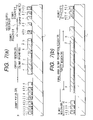
FIG. 7( a) and FIG. 7( b) are sectional views showing an example of a method of manufacturing the semiconductor integrated circuit device according to the embodiment as a sequence of processes.
FIG. 8( a) and FIG. 8( b) are sectional views showing an example of a method of manufacturing the semiconductor integrated circuit device according to the embodiment as a sequence of processes.
FIG. 9( a) and FIG. 9( b) are sectional views showing an example of a method of manufacturing the semiconductor integrated circuit device according to the embodiment as a sequence of processes.
FIG. 10( a) and FIG. 10( b) are sectional views showing an example of a method of manufacturing the semiconductor integrated circuit device according to the embodiment as a sequence of processes.
FIG. 11( a) and FIG. 11( b) are sectional views showing an example of a method of manufacturing the semiconductor integrated circuit device according to the embodiment as a sequence of processes.
FIG. 12( a) and FIG. 12( b) are sectional views showing an example of a method of manufacturing the semiconductor integrated circuit device according to the embodiment as a sequence of processes.
FIG. 13( a) and FIG. 13( b) are sectional views showing an example of a method of manufacturing the semiconductor integrated circuit device according to the embodiment as a sequence of processes.
FIG. 14( a) and FIG. 14( b) are sectional views showing an example of a method of manufacturing the semiconductor integrated circuit device according to the embodiment as a sequence of processes.
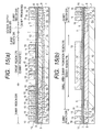
FIG. 15( a) and FIG. 15( b) are sectional views showing an example of a method of manufacturing the semiconductor integrated circuit device according to the embodiment as a sequence of processes.
FIG. 16( a) and FIG. 16( b) are sectional views showing an example of a method of manufacturing the semiconductor integrated circuit device according to the embodiment as a sequence of processes.
FIG. 17 is a plan view showing an example of a method of manufacturing the semiconductor integrated circuit device according to the embodiment as part of a sequence of processes.
FIG. 18 is an enlarged plan view of FIG. 17.
FIG. 19( a) and FIG. 19( b) are sectional views showing an example of a method of manufacturing the semiconductor integrated circuit device according to the embodiment as a sequence of processes.
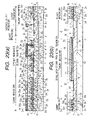
FIG. 20( a) and FIG. 20( b) are sectional views showing an example of a method of manufacturing the semiconductor integrated circuit device according to the embodiment as a sequence of processes.
FIG. 21( a) and FIG. 21( b) are sectional views showing an example of a method of manufacturing the semiconductor integrated circuit device according to the embodiment as a sequence of processes.
FIG. 22( a) and FIG. 22( b) are sectional views showing an example of a method of manufacturing the semiconductor integrated circuit device according to the embodiment as a sequence of processes.
FIG. 23( a) and FIG. 23( b) are sectional views showing an example of a method of manufacturing the semiconductor integrated circuit device according to the embodiment as a sequence of processes.
FIG. 24 is a plan view showing an example of a method of manufacturing the semiconductor integrated circuit device according to the embodiment as part of a sequence of processes.
FIG. 25 is an enlarged plan view showing another example of the semiconductor integrated circuit device according to the embodiment.
FIG. 26 is an enlarged plan view showing another example of the semiconductor integrated circuit device according to the embodiment.
FIG. 27 is an enlarged plan view showing yet another example of the semiconductor integrated circuit device according to the embodiment.
FIG. 28 is an enlarged plan view showing yet another example of the semiconductor integrated circuit device according to the embodiment.
DESCRIPTION OF THE PREFERRED EMBODIMENTS
One embodiment of this invention will now be described in detail with reference to the drawings. In all of the drawings which illustrate this embodiment, the same symbols are used for members having identical functions, and their description will not be repeated.
FIG. 1 is a plan view showing a silicon wafer used for manufacturing a semiconductor integrated circuit device according to one embodiment of the invention. A notch In is made in a single crystal silicon wafer 1 w and serves as a crystal plane index mark of the wafer 1 w. A chip 1 c is formed on the wafer 1 w. The chip 1 c is formed in the effective processing area of the wafer 1 w, and a chip region 1 g outside the effective processing area is not used.
FIG. 2 is a plan view showing an enlargement of the chip 1 c of the wafer 1 w. The chip 1 c is scribed and divided by a scribe line SL. In the steps described hereafter, each step is performed in the state of the wafer 1 w, the chip 1 c being divided in the final step.
In this form of the invention, the typical DRAM chip 1 c is shown as an example. It may also be another product, for example a logic product, such as a CPU, a memory element, such as an SRAM (Static Random Access Memory), or a memory which can be erased in one step and be electrically rewritten (so-called EEPROM: Electrical Erasable Read Only Memory), or a system LSI where a logic circuit and memory element coexist on the same chip. A memory cell array MA, direct peripheral circuit PCd and indirect peripheral circuit Pci are formed in the chip 1 c. DRAM memory cells are formed in the memory cell array MA. The direct peripheral circuit PCd is formed on the periphery of the memory cells MA. The indirect peripheral circuit Pci is formed in the center region of the chip 1 c.
FIG. 3 is a plan view showing an edge region of the chip 1 c comprising the region of the scribe line SL. FIG. 3 shows the state where an isolation region is formed on a semiconductor substrate 1 (wafer 1 w, chip 1 c). The regions other than a scribe region SR are product regions PR.
A target pattern T1, large area dummy pattern DL and small area pattern Ds are formed simultaneously when the isolation region is formed in the scribe region SR. A TEG (Test Equipment Group) element is also formed in the scribe region SR, but it is not shown in the drawings. The target pattern T1 is a pattern formed simultaneously in a step when an isolation region pattern is formed, and it is used for alignment in an exposure step when a gate electrode pattern, to be described later, is formed. Specifically, it is used as a target for position detection when mask alignment of a target electrode pattern is performed. In an exposure device, a mask is aligned with respect to the wafer by, for example, performing optical pattern recognition of the target, and a photoresist film is then exposed.
The large area dummy pattern DL and small area dummy pattern Ds are patterns which are simultaneously formed in the step when the isolation region pattern is formed. A target pattern T2 is formed simultaneously with the target electrode pattern on the large area dummy pattern DL. The target pattern T2 is used for alignment in the exposure step when the upper layer pattern, for example, an interconnection pattern or connecting hole pattern, is formed. Due to the provision of the large area pattern DL, dishing in the target pattern region is prevented, the recognition rate of the target pattern is improved, and fine patterning can advantageously be performed. In the prior art, a dummy pattern was not provided on the periphery of the prior art target pattern, so that the surface flatness of the target pattern periphery was impaired; however, by providing the large area dummy pattern DL underneath the target pattern, the flatness is improved and the recognition rate of the target pattern is improved. The large area dummy pattern DL is formed to be larger than the target pattern so as to enclose the target pattern. In other words, the large area dummy pattern DL is present underneath the target pattern region used for optical pattern recognition, so that dishing is prevented and the recognition rate of the target pattern is improved. On the periphery of the target pattern, there is a region where any kind of pattern is prohibited, thereby to prevent interference with target pattern recognition. The large area dummy pattern DL has an area equal to or greater than this pattern prohibition region. Therefore, the large area dummy pattern DL is not recognized as a pattern by the exposure device, and the recognition rate of the target patterns T1, T2 is not decreased.
The small area dummy pattern Ds is formed in the scribe region SR and the product region PR. In other words, it is formed over the whole surface of the wafer W. Thus, the small area dummy pattern Ds is disposed in a region in which there is a wide interval between patterns functioning as elements. Since there is a wide interval between patterns functioning as elements, if the small area dummy pattern Ds were not disposed in this wide pattern interval, dishing would occur in the pattern interval. Since this dishing becomes larger in depth as the pattern interval becomes wider, the flatness is largely impaired. By disposing this small area dummy pattern Ds in this wide inter-pattern space, the flatness is improved. As the pattern size and inter-pattern space are formed with dimensions of approximately the same order as those of the pattern forming the elements, the pattern interval is narrow, and a small amount of dishing according to the narrow pattern interval occurs. In this situation, the depression amount can be much improved and the flatness can be improved compared with the case when the dummy pattern is not provided. The pattern size of the small area dummy pattern Ds is of the same order as the element design rule, and a suitable value is selected with regard to the ease of photolithography and the effect on suppression of dishing. When the element design rule is of the order of, for example, 0.2 μm, the pattern size of the small area dummy pattern Ds may also be set to the order of 0.2 μm. However, if a KrF excimer laser is used as the exposure light source, a technique must be used to improve the resolution, such as use of a Levenson mask. If priority is given to the ease of forming the mask, the pattern size of the small area dummy pattern Ds may be set to be of the order of 1 μm, and the inter-pattern space may be set to be of the order of 0.4 μm. It will of course be understood that other figures can be selected from the requirements of the photolithography step. However, if the pattern size and inter-pattern space are too large, dishing in the inter-pattern space becomes more marked, which is undesirable.
The width of the scribe region SR is approximately 100 μm.
In FIG. 3, active regions which form elements are formed apart from the aforesaid small area dummy pattern Ds in the product region PR. According to this embodiment, an active region L1 forming a channel region of a MISFET (Metal Insulator Semiconductor Field Effect Transistor), an active region L2 for well feed and an active region L3 for guard band feed are shown as examples. It will be understood that other active regions may also be formed. The aforesaid small area dummy pattern Ds is formed between the patterns of the active regions L1, L2, L3. The large area dummy pattern DL may also be formed in the product region PR.
FIG. 4 is a plan view showing an enlargement of a region comprising the active regions L1, L2 of the product region PR. Plural small area dummy patterns Ds are disposed between the patterns of the active regions L1, L2, as described above. As stated above, the pattern size d1 of the small area dummy pattern Ds is approximately 1 μm, and the pattern interval S1 is approximately 0.4 μm.
The small Area dummy pattern Ds is formed by automatically generating patterns of the aforesaid size in a lattice (grid) with the pattern pitch (1.4 μm in the case of this embodiment). At each lattice point, the small area dummy pattern Ds is not generated in parts where the active regions L1, L2 are present. Specifically, in a mask design device, a graphic computation is performed which expands patterns such as the active regions L1, L2. This expanded pattern region is a pattern prohibition region R1 of the small area dummy pattern Ds. Next, of the aforesaid lattice points, the lattice within the pattern prohibition region R1 is excluded from the graphic computation, and the small area dummy pat@ern Ds is generated at the remaining lattice points. This generated small area dummy pattern Ds is added to the active regions R1, R2 to give mask generation data. The pattern prohibition region R1 for the small area dummy pattern Ds is formed also on the periphery of the large area dummy pattern DL. As a result, the pattern to be expanded also contains the large area dummy pattern DL. In this way, a mask pattern wherein dummy patterns are disposed is easily generated automatically. This can also be done manually or automatically by disposing a layer (pattern layer) corresponding to the pattern prohibition region R1, and then specifying positions where it is not desired to dispose other small area dummy patterns Ds.
Next, the method of manufacturing the semiconductor integrated circuit device of this invention will be described, including the steps for forming the aforesaid active regions and a dummy region (isolation region) DR.
FIG. 5 to FIG. 23 (excluding FIG. 17, FIG. 18) are sectional views showing the sequence of steps in one example of the method of manufacturing the semiconductor integrated circuit device of this invention. In these sectional views, figures with numbers to which (a) is appended represent a section as seen on a line A—A in FIG. 3 and FIG. 4, and figures with numbers to which (b) is appended represent a section through a line B—B in FIG. 3. In the (a) figures, the dummy region DR where a dummy pattern is formed, circuit region CR and voltage supply region SR where a voltage supply pattern is formed, are respectively shown. In the (b) figures, a target region TR, small area dummy pattern prohibition region IR and dummy region DR are respectively shown.
As shown in FIGS. 5( a) and 5(b), the semiconductor substrate 1 (wafer 1 w) is provided, and a thin silicon oxide (SiO) film 2 and silicon nitride (SiN) film 3 are formed thereon. The semiconductor substrate 1 is a single crystal silicon wafer wherein, for example, p type impurities are introduced, and it has a resistivity of the order of several ohm cm. The silicon oxide film 2 is a sacrifice film for alleviating the stress between the silicon nitride film 3 and semiconductor substrate 1, and it is formed, for example, by thermal oxidation. The silicon nitride film 3 is used as a mask for forming a groove, as will be described later. The film thickness of the silicon nitride film 3 is several hundred nm, and it is formed for example by CVD (Chemical Vapor Deposition).
Next, as shown in FIGS. 6( a) and 6(b), a photoresist film 4 is formed on the silicon nitride film 3. The photoresist film 4 is formed to cover the regions where the active regions L1, L2, L3, the large area dummy pattern DL and the small area dummy pattern Ds, which were described in FIG. 3 and FIG. 4, are respectively formed. As stated above, regarding the size of the small area dummy pattern Ds, the fine patterning which would be required with a Levenson mask is not necessary, so that in the region where the small area dummy pattern Ds is formed, there is no impairment of machinability due to the decrease of focal point tolerance that is inherent in super-high resolution techniques, such as the Levenson method. This simplifies the mask design.
Next, as shown in FIGS. 7( a) and 7(b), dry etching is performed in the presence of the photoresist film 4, and the silicon nitride film 3 and silicon oxide film 2 are etched to remove them.
After the photoresist film 4 is removed, as shown in FIGS. 8( a) and 8(b), dry etching (anisotropic etching) is performed in the presence of the silicon nitride film 3, and the semiconductor substrate 1 is etched to form a groove S. The depth of the groove 5 is several hundred nm. The pattern of the groove 5 formed in this step is the reverse of the pattern of the active regions L1, etc., shown in the aforesaid FIG. 3 and FIG. 4.
In this step, the patterned silicon nitride film 3 is used as a hard mask. By using the thin silicon nitride film 3 as a hard mask, the etching properties are improved, and fine patterning can easily be performed. Instead of using the silicon nitride film 3 as a hard mask, the semiconductor substrate 1 can be etched in the presence of the photoresist film 4 to form the groove 5. In this case, the steps are simplified.
Next, as shown in FIGS. 9( a) and 9(b), a silicon oxide film 6 is formed over the whole surface of the semiconductor substrate 1, including the interior of the groove 5. The silicon oxide film 6 can be formed by CVD using, for example, TEOS (tetraethoxysilane) gas and ozone (O3) as raw material gases. The film thickness of the silicon oxide film 6 is a film thickness sufficient to fill the groove 5.
Next, as shown in FIGS. 10( a) and 10(b), the silicon oxide film is polished using CMP. The polishing is performed until the surface of the silicon nitride film 3 is exposed. In this way, the isolation region 7 is formed leaving the silicon oxide film 6 only in the region of the groove 5.
In this process, in the dummy region DR, the small area dummy pattern Ds is formed, so dishing occurs only slightly between the patterns of the small area dummy pattern Ds, and the flatness can be remarkably improved compared with the case where the dummy pattern is not present. Further, as the large area dummy pattern DL is formed also in the target region TR, global dishing is prevented, and the flatness in this region is improved. In the case of this embodiment, the target region TR is formed in the scribe region SR, and deterioration of the flatness in the target region TR may occasionally cause a decrease in the flatness in the product region PR, which is adjacent to the target region TR. However, according to this embodiment, the large area pattern DL is formed in the target region TR, so there is no such effect on the product region PR.
Next, as shown in FIGS. 11( a) and 11(b), the silicon nitride film 3 and silicon oxide film 2 are removed to expose the active regions L1, L2, L3, large area dummy pattern DL and small area dummy pattern Ds. The aforesaid FIG. 3 and FIG. 4 show the stage when this step is completed. To remove the silicon nitride film 3, wet etching with hot phosphoric acid is used, for example. Subsequently, the surfaces of the silicon oxide film 2 and isolation region 7 are etched to a suitable degree by hydrofluoric acid (HF), and the substantially flat surface shown in FIGS. 11( a) and 11(b) is obtained.
Next, as shown in FIGS. 12( a) and 12(b), a photoresist film, not shown, is formed; p type or n type impurities are ion implanted; and a deep well 8, n type well 9 and p type well 10 are formed. The deep well 8 functions to electrically isolate the p type well 10 from the semiconductor substrate 1.
Next, as shown in FIGS. 13( a) and 13(b), a silicon oxide film 11, polycrystalline silicon film 12 and tungsten silicide (WSi) film 13, which function as a gate electrode, and a silicon nitride film 14, which functions as a gap insulating film, are deposited. The silicon nitride film 11 is formed, for example, by thermal oxidation or by thermal CVD, and has a film thickness of several nm. The polycrystalline silicon film 12 is formed, for example, by CVD, and n type or p type impurities are introduced into it. The film thickness is several hundred nm. The tungsten silicide film 13 is formed by CVD or by sputtering, and likewise, the film thickness is several hundred nm. The tungsten silicide film 13 decreases the sheet resistance of the gate electrode (gate interconnection) and contributes to improving the response speed of the element. The silicon nitride film 14 is formed, for example, by CVD, and has a film thickness of several hundred nm.
Here, the tungsten silicide film 13 was shown as an example, but other metal silicide films, such as a titanium silicide (TiSi) film or a cobalt silicide (CoSi) film may be used. Also, a laminate comprising the tungsten silicide film 13 and polycrystalline silicon film 12 was shown as an example, but laminates of the polycrystalline silicon film, a barrier film and a metal film, such as tungsten (W), may be used. In this case, the resistivity of the gate electrode (gate interconnection) can be further reduced. A metal nitride film, such as tungsten nitride (WN), titanium nitride (TiN) or tantalum nitride (TaN), may be used for the barrier film. In addition to tungsten, tantalum (Ta) or titanium (Ti) can also be used for the metal film.
Next, as shown in FIGS. 14( a) and 14(b), a photoresist film 15 is formed on the silicon nitride film 14, and dry etching (anisotropic etching) is performed to pattern the silicon nitride film 14, as shown in FIGS. 15( a) and 15(b). In this way, a gap insulating film 16 is formed. The patterning of this gap insulating film 16 will be described later. In the exposure step for forming the photoresist film 15, the target T1 is used for position detection in mask alignment.
Next, the photoresist film 15 is removed by ashing or the like, and the tungsten silicide film 13, polycrystalline silicon film 12 and silicon oxide film 11 are etched (anisotropically etched) in the presence of the gap insulating film 16 to form a gate electrode 17, as shown in FIGS. 16( a) and 16(b).
At this time, a second small area dummy pattern Ds2 and target T2 are formed simultaneously with the gate electrode 17.
FIG. 17 is a plan view showing the situation at this stage, corresponding to FIG. 3. FIG. 18 is an enlarged plan view corresponding to FIG. 4.
As shown in FIG. 17, the target T2 is formed in addition to the small area dummy pattern Ds2 in the scribe region SR. The target T2 is used for exposure, for example in a step to form interconnections or connection holes. The target T2 is formed on the large area dummy pattern DL so as to be enclosed by it. The pattern prohibition region R2 is also formed on the periphery of the target T2 to prevent a decrease in the recognition rate when the target T2 is used later, and the large area dummy pattern DL is formed to be larger than the pattern prohibition region R2. Hence, no pattern other than the target T2 is formed inside the pattern prohibition region R2, so that the target T2 can be accurately recognized. Further, since the target T2 is formed on the large area dummy pattern DL, the target T2 is not formed on a depressed substrate, but is formed on a flattened substrate. Therefore, in a subsequent exposure step using the target T2, the target T2 can be accurately recognized, and the mask alignment precision is improved. Further, since the large area dummy pattern DL is formed underneath the target T2, the flatness of this region is improved, the flatness of its periphery, in particular the product region PR adjacent to the target T2, is improved, which results in an improvement of the photolithography margin, and etching is easily performed.
The small area dummy pattern Ds2 is also formed in the scribe region SR. This improves the flatness of this region. However, it is not disposed in the small area dummy pattern prohibition region R1. The small area dummy pattern Ds2 will be described later.
The gate electrode 17 is formed in the product region PR. Plural small area dummy patterns Ds2 are disposed between the patterns of the gate electrode 17. As in the case of FIG. 3, they are not disposed in the small area dummy pattern prohibition region R2. The pattern prohibition region R1 is formed in the same way as described above.
The small area dummy pattern Ds2 is formed on the inter-pattern spaces of the small area dummy pattern Ds of the lower layer, as shown in FIG. 18. Specifically, the pitch of the small area dummy pattern Ds2 and that of the small area dummy pattern Ds in the layer underneath are offset by ½. In other words, the small area dummy pattern Ds2 is offset by Px in the x direction and by Py in the y direction with respect to the small area dummy pattern Ds. Px, Py are, for example, both 0.7 μm. In this way, by forming the small area dummy pattern Ds2 with an offset of ½ pitch, the effect of dishing in the layer underneath is eliminated and the flatness is improved. In other words, the dishing of the layer underneath occurs in a space part of the small area dummy pattern Ds, and since the small area dummy pattern Ds2 is formed on top of it, the dishing is not superimposed. Dishing due to the small area dummy pattern Ds2 occurs in its space part, but as the small area dummy pattern Ds is formed in the layer underneath it, dishing does not occur here. In other words, by providing the small area dummy patterns Ds, Ds2 as in this embodiment, dishing does not occur in the layer above the region where dishing occurs in the lower layer, and the part where dishing occurs in the upper layer is formed over the region where dishing does not occur in the lower layer. Hence, the total amount of dishing due to the two layers is reduced, and the overall flatness can be increased.
The situation wherein the small area dummy pattern Ds2 of the upper layer is not formed in the pattern prohibition region R1 is identical to the case of the small area dummy pattern Ds. Further, the small area dummy pattern Ds2 is generated in an identical way to the small area dummy pattern Ds, except that the lattice positions are shifted by ½ pitch.
Herein, a case was described where the small area dummy patterns Ds, Ds2 were shifted by ½ pitch, but the shift amount may be any value provided that the side edge of Ds2 is formed to overlap with Ds1. In other words, Ds2 must be formed in a part above the space part of Ds1.
Next, impurities are ion-implanted to form an impurity semiconductor region 19, as shown in FIGS. 19( a) and 19(b). Low concentrations of impurities are introduced into the impurity semiconductor region 19. The conductivity of the impurity introduced is chosen according to the channel type of the MISFET that is being formed. Thus, p type impurities are implanted in an n type well region to form a p channel MISFET; and, n type impurities are introduced in a p well region to form an n channel MISFET.
Next, as shown in FIGS. 20( a) and 20(b), a silicon nitride film, for example, is formed over the whole surface of the semiconductor substrate 1, and this is subjected to anisotropic etching to form a side wall spacer 20. Subsequently, ion implantation is performed to form an impurity semiconductor region 21. The impurity ions introduced into the impurity semiconductor region 21 are chosen to give a suitable conductivity depending on the region, as in the case described above. High concentrations of impurities are introduced into the impurity semiconductor region 21, and a source/drain having an LDD (Lightly Doped Drain) structure is formed together with the impurity semiconductor region 19.
Next, as shown in FIGS. 21( a) and 21(b), a silicon oxide film 22 enclosing the gate electrode pattern is formed, and as shown in FIGS. 22( a) and 22(b), the silicon oxide film 22 is polished by CMP to flatten its surface. During this flattening, since the small area dummy pattern Ds2 is formed in the same layer as the gate electrode pattern, the flatness is improved. In particular, since the small area dummy pattern Ds2 is offset by ½ pitch with respect to the small area dummy pattern Ds of the lower layer, the dishing of the two layers in the spaces between the patterns is not superimposed. As a result, a decrease of the flatness due to superimposition of dishing is suppressed. Also, in the region of the target T2, since the large area dummy pattern DL is formed in the layer underneath, global dishing does not occur, and the flatness is improved also in the scribe region SR. Hence, there is no adverse effect on the product region PR, and the yield is improved. Moreover, the small area dummy pattern Ds2 is also disposed in the scribe region SR, so that the flatness is improved in the same way as in the product region PR.
Herein, a case was described wherein the target T2 was formed in the scribe region SR, but the target T2 may also be formed in the product region PR. Further, the target pattern was given as an example of a pattern required for pattern recognition, but it will be understood that the invention may also be applied to any pattern which can be used for optical pattern recognition. For example, it may be a testing pattern used for quality control in mask alignment, a test pattern for monitoring the film thickness, or a position detecting pattern used for laser repair.
Next, as shown in FIGS. 23( a) and 23(b), a connecting hole 23 is formed in the silicon oxide film 22, and a connecting plug 24 is formed in the connection hole 23. An interconnection 25 is also formed on the silicon oxide film 22.
The connecting hole 23 is formed by anisotropic etching using a photoresist film, not shown, as a mask. When this photoresist film is formed, i.e., for the exposure of this step, the aforesaid target T2 may be used for position detection in mask alignment. In addition to polycrystalline silicon, laminates of titanium nitride films and tungsten films may, for example, be used for the connecting plug. To form the connecting plug, a connecting hole is opened, an electrically conducting material is formed to fill it, and the electrically conducting film in regions other than the connecting hole is removed by CMP.
The interconnection 25 is formed by anisotropic etching using a photoresist film, not shown, in the same way. When this photoresist film is formed, i.e. for the exposure of this step, the aforesaid target T2 may be used for position detection in mask alignment. Metal materials, such as tungsten and laminates of, for example, titanium nitride and tungsten, may be used for the interconnection 25. The interconnection 25 is formed by forming a film of the metal material, and patterning it.
A multilayer interconnection structure can be formed by forming interconnections in the upper layers, such as the second and third layers, and since this is identical to the case of the aforesaid interconnection 25, its description will be omitted.
FIG. 24 is a plan view showing the situation when the wafer process is complete, and the scribe region SR is at the scribe stage. The wafer 1 w is divided by the scribe line SL to form the chip 1 c. The width of the scribe line SL is a dimension obtained by adding play to the blade width (e.g., 35 μm) As a result, in the chip 1 c, a region of the order of several tens of μm remains as the distance from the edge of the product region PR to the edge of the chip 1 c. Part of the aforesaid targets T1, T2, and the large area dummy pattern DL, remain in this residual region. In FIG. 24, a target T3 is shown. This is a target pattern formed simultaneously when the interconnection 25 of the first layer is patterned. The target T3 is used to form an interconnection or through hole in the upper layer.
This invention as conceived by the inventors has been described in detail based on one embodiment of the invention, however it will be understood that the invention is not limited to this embodiment, various modifications being possible within the scope and spirit of the appended claims.
For example, in the embodiment, an example was given where the offset of the small area dummy patterns Ds, Ds2 was provided in both the x direction and y direction, but the offset may be provided in only one direction.
Further, the case was shown where the small area dummy patterns Ds, Ds2 were rectangular, but they may also be of another shape, such as oblong. For example, they may be lattice-shaped dummy patterns, as shown in FIG. 25 and FIG. 26. Specifically, a lattice-shaped pattern 26 can be formed simultaneously with the active region L1, as shown in FIG. 25, or a lattice-shaped pattern 27 can be simultaneously formed with the gate electrode 17 with a ½ pitch shift relative to the pattern 26, as shown in FIG. 26. Alternatively, instead of the small area target patterns Ds, Ds2, line-shaped dummy patterns can be formed, as shown in FIG. 27 and FIG. 28. Specifically, a line-shaped dummy pattern 28 can be formed simultaneously with the active region L1, as shown in FIG. 27, or a line-shaped pattern 29 can be simultaneously formed with the gate electrode 17 with a ½ pitch shift relative to the pattern 28, as shown in FIG. 28. These dummy patterns 26, 27, 28, 29 are not formed in the pattern prohibition region R1, which is identical to the case of the embodiment. Further, the sizes of the patterns 26, 27, 28, 29 are also identical to those of the embodiment.
Among the inventive features disclosed in this application, the effects obtained by representative aspects of the invention may simply be described as follows.
(1) Dishing in plural laminated flattened surfaces is suppressed.
(2) Surface flattening in pattern regions of a large area for optical position detection, e.g., of targets, is improved.
(3) The flatness of plural laminated surfaces, or the flatness of large area patterns, such as targets, is improved, and the machining margin in a photolithography step and etching step is improved.

Claims (69)

1. A semiconductor integrated circuit device comprising:
a semiconductor substrate having a semiconductor element formed over a main surface of the semiconductor substrate;
an isolation region formed on said semiconductor substrate;
an active region formed on said semiconductor substrate, which is surrounded by said isolation region; and
a conductive layer formed over said active region, wherein:
said active region comprises a dummy active region,
said conductive layer comprises a pattern used for optical pattern recognition, and
said dummy active region is formed directly under the whole area of said pattern used for optical pattern recognition.
2. A semiconductor integrated circuit device according to claim 1, wherein said dummy active region is formed at a scribing region.
3. A semiconductor integrated circuit device comprising:
a semiconductor substrate having a semiconductor element formed over a main surface of said semiconductor substrate;
a first pattern formed on said main surface or on any layer over said main surface, wherein said first pattern comprises a dummy pattern;
a second pattern formed over an upper layer of said first pattern, wherein said second pattern comprises a pattern used for optical pattern recognition; and
means for preventing dishing of said semiconductor integrated circuit device in a whole area directly under the pattern used for optical pattern recognition.
4. A semiconductor integrated circuit device according to claim 3, wherein said means comprises forming said dummy pattern to be located directly under the whole area of said pattern used for optical pattern recognition.
5. A semiconductor integrated circuit device according to claim 3, wherein said dishing preventing means is formed at a scribing region.
6. A semiconductor integrated circuit device comprising:
a semiconductor substrate having a first region and a second region;
a MISFET having an active region and a gate electrode, formed in said first region;
a plurality of grooves in said first and second regions;
a plurality of first insulating films formed in said grooves in said first and second regions;
a plurality of said conductors formed over said grooves in said second region, wherein said plurality of conductors are formed on the same level as a conductor forming said gate electrode in said first region; and
a second insulating film formed over said conductors in said first and second regions,
wherein said active region is formed between said adjacent grooves in said first region,
wherein said plurality of conductors in said second region are isolated from each other,
wherein said first and second insulating films are polished by a CMP method, and
wherein areas located in said second region are surrounded by trenches in said second region and are disposed to be spaced apart from one another by a certain distance, and,
said conductors in said second region are spaced apart from one another by said same certain distance.
7. A semiconductor integrated circuit device as defined in claim 6, wherein said first insulating films in said grooves form shallow groove isolations.
8. A semiconductor integrated circuit device as defined in claim 6, wherein said first and second insulating films are flattened by said CMP method.
9. A semiconductor integrated circuit device as defined in claim 6, wherein one of the side edges of each of said conductors is formed so as to overlap with one of said areas located in said second region when viewed in a plan view direction parallel to a main surface of said semiconductor substrate.
10. A semiconductor integrated circuit as defined in claim 6, wherein said areas located in said second region and said conductors are offset by a distance of ½ pitch when viewed in a plan view direction parallel to a main surface of said semiconductor substrate.
11. A semiconductor integrated circuit device according to claim 1, wherein a groove is formed in said substrate and defines said active region and dummy regions,
wherein an isolation film is filled in said groove by polishing an insulating film formed over said groove and said substrate so as to form said isolation region, and
wherein said active region and said dummy regions are formed at a scribing area.
12. A semiconductor integrated circuit device according to claim 11, wherein said dummy regions are formed to surround said active region.
13. A semiconductor integrated circuit device according to claim 3, wherein a groove is formed in said substrate and defines said dishing preventing means and dummy regions,
wherein an isolation film is filled in said groove by polishing an insulating film formed over said groove and said substrate, and
wherein said dishing preventing means and said dummy regions are formed at a scribing area such that said dummy regions are formed to surround said dishing preventing means.
14. A semiconductor integrated circuit device according to claim 6, wherein said conductors comprise a pattern used for optical recognition, and
wherein said second region is a scribing region.
15. A semiconductor integrated circuit device according to claim 6, wherein said grooves are formed in said substrate and define said active region and dummy regions,
wherein said first region and said dummy regions are formed at a product region, and
wherein said second region and said dummy regions are formed at said scribing area such that said dummy regions are formed to surround said second region.
16. A semiconductor integrated circuit device comprising:
a groove formed in a semiconductor substrate and defining active regions and dummy regions,
said dummy regions including a first dummy region and second dummy regions such that said first dummy region has an area greater than individual areas of each of said second dummy regions;
an element isolation insulating film filled in said groove by polishing an insulating film formed over said groove such that said element isolation insulating film serves as an element isolation region; and
a conductor pattern formed over said first dummy region and used for optical pattern recognition,
wherein said second dummy regions are formed at a product region and at a scribing region, and
wherein said first dummy region is formed at said scribing region.
17. A semiconductor integrated circuit device according to claim 16, wherein said second dummy regions are formed to surround said first dummy region.
18. A semiconductor integrated circuit device according to claim 16, wherein said conductor pattern is formed with the same level layer as a gate electrode of a MISFET formed over said active region.
19. A semiconductor integrated circuit device according to claim 16, wherein said conductor pattern is larger than said first dummy region so as to enclose said first dummy region.
20. A semiconductor integrated circuit device comprising:
a groove formed in a semiconductor substrate and defining active regions and dummy regions,
said dummy regions including a first dummy region and second dummy regions such that said first dummy region has an area greater than individual areas of each of said second dummy regions;
an element isolation insulating film filled in said groove by polishing an insulating film formed over said groove such that said element isolation insulating film serves as an element isolation region; and
a conductor pattern formed over said first dummy region and used for optical pattern recognition,
wherein said first dummy region and said second dummy regions are formed at a scribing region.
21. A semiconductor integrated circuit device according to claim 20, wherein said second dummy regions are formed to surround said first dummy region.
22. A semiconductor integrated circuit device according to claim 20, wherein said conductor pattern is formed with the same level layer as a gate electrode of a MISFET formed over said active region.
23. A semiconductor integrated circuit device according to claim 20, wherein said conductor pattern is larger than said first dummy region so as to enclose said first dummy region.
24. A semiconductor integrated circuit device comprising:
grooves formed in a semiconductor substrate and defining active regions and dummy regions,
said dummy regions including a first dummy region and second dummy regions such that said first dummy region has an area greater than individual areas of each of said second dummy regions;
element isolation insulating films filled in said grooves by polishing an insulating film formed over said grooves such that said element isolation insulating films serve as element isolation regions; and
a conductor pattern formed over said first dummy region and used for optical pattern recognition,
wherein said second dummy regions are formed at a product region and at a scribing region, and
wherein said first dummy region is formed at said scribing region.
25. A semiconductor integrated circuit device according to claim 24, wherein said second dummy regions are formed to surround said first dummy region.
26. A semiconductor integrated circuit device according to claim 24, wherein said conductor pattern is formed with the same level layer as a gate electrode of a MISFET formed over said active region.
27. A semiconductor integrated circuit device according to claim 24, wherein said conductor pattern is larger than said first dummy region so as to enclose said first dummy region.
28. A semiconductor integrated circuit device comprising:
grooves formed in a semiconductor substrate and defining active regions and dummy regions,
said dummy regions including a first dummy region and second dummy regions such that said first dummy region has an area greater than individual areas of each of said second dummy regions;
element isolation insulating films filled in said grooves by polishing an insulating film formed over said grooves such that said element isolation insulating films serve as an element isolation region; and
a conductor pattern formed over said first dummy region and used for optical pattern recognition,
wherein said first dummy region and second dummy regions are formed at a scribing region.
29. A semiconductor integrated circuit device according to claim 28, wherein said second dummy regions are formed to surround said first dummy region.
30. A semiconductor integrated circuit device according to claim 28, wherein said conductor pattern is formed with the same level layer as a gate electrode of a MISFET formed over said active region.
31. A semiconductor integrated circuit device according to claim 28, wherein said conductor pattern is larger than said first dummy region so as to enclose said first dummy region.
32. A semiconductor integrated circuit device comprising:
a first groove and a second groove formed in a semiconductor substrate,
said first groove defining a first dummy region and second dummy regions such that said first dummy region has an area greater than individual areas of each of said second dummy regions;
said second groove defining an active region;
element isolation insulating films filled in said first groove and said second groove by polishing an insulating film formed over said first groove and said second groove; and
a conductor pattern formed over said first dummy region and used for optical pattern recognition,
wherein said first dummy region and said second dummy regions are formed at a scribing region.
33. A semiconductor integrated circuit device according to claim 32, wherein said active region is formed at a product region.
34. A semiconductor integrated circuit device according to claim 32, wherein said first groove is integrally formed with said second groove.
35. A semiconductor integrated circuit device according to claim 32, wherein said conductor pattern is formed with the same level layer as a gate electrode of a MISFET formed over said active region.
36. A semiconductor integrated circuit device according to claim 32, wherein said conductor pattern is larger than said first dummy region so as to enclose said first dummy region.
37. A semiconductor integrated circuit device comprising:
a first groove and a second groove formed in a semiconductor substrate,
said first groove defining a first dummy region and second dummy regions such that said first dummy region has an area greater than individual areas of each of said second dummy regions;
said second groove defining an active region and third dummy regions;
element isolation insulating films filled in said first groove and said second groove by polishing an insulating film formed over said groove and said second groove; and
a conductor pattern formed over said first dummy region and used for optical pattern recognition,
wherein said first dummy region and said second dummy regions are formed at a scribing region.
38. A semiconductor integrated circuit device according to claim 37, wherein said active region and third dummy regions are formed at a product region.
39. A semiconductor integrated circuit device according to claim 37, wherein said first groove is integrally formed with said second groove.
40. A semiconductor integrated circuit device according to claim 37, wherein said conductor pattern is formed with the same level layer as a gate electrode of a MISFET formed over said active region.
41. A semiconductor integrated circuit device according to claim 37, wherein said conductor pattern is larger than said first dummy region so as to enclose said first dummy region.
42. A semiconductor integrated circuit device comprising:
a groove formed in a semiconductor substrate and defining active regions and a dummy region;
an element isolation insulating film filled in said groove by polishing an insulating film formed over said groove such that said element isolation insulating film serves as an element isolation region; and
a conductor pattern formed over said dummy region and used for optical pattern recognition,
wherein said dummy region is formed at said scribing region, and
wherein an area of said dummy region is larger than that of said conductor pattern such that the whole area of said conductor pattern is arranged over said dummy region.
43. A semiconductor integrated circuit device according to claim 42, wherein said conductor pattern is formed with the same level layer as a gate electrode of a MISFET formed over said active region.
44. A semiconductor integrated circuit device comprising:
grooves formed in a semiconductor substrate and defining active regions and a dummy region;
element isolation insulating films filled in said grooves by polishing an insulating film formed over said grooves such that said element isolation insulating films serve as element isolation regions; and
a conductor pattern formed over said dummy region and used for optical pattern recognition,
wherein said dummy region is formed at said scribing region, and
wherein an area of said dummy region is larger than that of said conductor pattern such that the whole area of said conductor pattern is arranged over said dummy region.
45. A semiconductor integrated circuit device according to claim 44, wherein said conductor pattern is formed with the same level layer as a gate electrode of a MISFET formed over said active region.
46. A semiconductor integrated circuit device comprising:
a first groove and a second groove formed in a semiconductor substrate,
said first groove defining a dummy region; said second groove defining a active region;
element isolation insulating films filled in said first groove and said second groove by polishing an insulating film formed over said first groove and said second groove; and
a conductor pattern formed over said dummy region and used for optical pattern recognition,
wherein said dummy region is formed at a scribing region, and
wherein an area of said dummy region is larger than that of said conductor pattern such that the whole area of said conductor pattern is arranged over said dummy region.
47. A semiconductor integrated circuit device according to claim 46, wherein said first groove is integrally formed with said second groove.
48. A semiconductor integrated circuit device according to claim 46, wherein said conductor pattern is formed with the same level layer as a gate electrode of a MISFET formed over said active region.
49. A semiconductor integrated circuit device comprising:
a first groove and a second groove formed in a semiconductor substrate,
said first groove defining a dummy region;
said second groove defining a active region;
element isolation insulating films filled in said first groove and said second groove by polishing an insulating film formed over said first groove and said second groove; and
a conductor pattern formed over said dummy region and used for optical pattern recognition,
wherein said dummy region is formed at a scribing region.
50. A semiconductor integrated circuit device according to claim 49, wherein said first groove is integrally formed with said second groove.
51. A semiconductor integrated circuit device according to claim 49, wherein said conductor pattern is formed with the same level layer as a gate electrode of a MISFET formed over said active region.
52. A semiconductor integrated circuit device according to claim 49, wherein an area of said dummy region is larger than that of said conductor pattern such that the whole area of said conductor pattern is arranged over said dummy region.
53. A semiconductor integrated circuit device comprising:
a groove formed in a semiconductor substrate and defining active regions and dummy regions,
said dummy regions including a first dummy region and second dummy regions such that said first dummy region has a area greater than an area of said second dummy region;
an element isolation insulating film filled in said groove by polishing an insulating film formed over said groove such that said element isolation insulating film serves as an element isolation region; and
wherein said first dummy region and said second dummy regions are formed at a scribing region.
54. A semiconductor integrated circuit device according to claim 53, wherein an area of said first dummy region is larger than that of said conductor pattern such that the whole area of said conductor pattern is arranged over said first dummy region.
55. A semiconductor integrated circuit device comprising:
a groove formed in a semiconductor substrate and defining active regions and dummy regions,
said dummy regions including a first dummy region and second dummy regions such that said first dummy region has an area greater than individual areas of said second dummy regions;
an element isolation insulating film filled in said groove by polishing an insulating film formed over said groove such that said element isolation insulating film serves as an element isolation region; and
a conductor pattern formed over said first dummy region and used for optical pattern recognition,
wherein said second dummy regions are formed at a product region, and
wherein said first dummy region is formed at a scribing region.
56. A semiconductor integrated circuit device according to claim 55, wherein said conductor pattern is formed with the same level layer as a gate electrode of a MISFET formed over said active region.
57. A semiconductor integrated circuit device according to claim 55, wherein an area of said first dummy region is larger than that of said conductor pattern such that the whole area of said conductor pattern is arranged over said first dummy region.
58. A semiconductor integrated circuit device comprising:
a groove formed in a semiconductor substrate and defining active regions and dummy regions,
said dummy regions including a first dummy region and second dummy regions such that said first dummy region has an area greater than individual areas of said second dummy regions;
an element isolation insulating film filled in said groove by polishing an insulating film formed over said groove such that said element isolation insulating film serves as an element isolation region; and
a conductor pattern formed over said first dummy region and used for optical pattern recognition.
59. A semiconductor integrated circuit device according to claim 58, wherein said second dummy regions are formed to surround said first dummy region.
60. A semiconductor integrated circuit device according to claim 58, wherein said conductor pattern is formed with the same level layer as a gate electrode of a MISFET formed over said active region.
61. A semiconductor integrated circuit device according to claim 58, wherein an area of said first dummy region is larger than that of said conductor pattern such that the whole area of said conductor pattern is arranged over said first dummy region.
62. A semiconductor integrated circuit device comprising:
grooves formed in a semiconductor substrate and defining active regions and dummy regions,
said dummy regions including a first dummy region and second dummy regions such that said first dummy region has an area greater than individual areas of said second dummy regions;
element isolation insulating films filled in said grooves by polishing an insulating film formed over said grooves such that said element isolation insulating films serve as element isolation regions; and
a conductor pattern formed over said first dummy region and used for optical pattern recognition,
wherein said second dummy regions are formed at a product region, and
wherein said first dummy region is formed at a scribing region.
63. A semiconductor integrated circuit device according to claim 62, wherein said second dummy regions are formed to surround said first dummy region.
64. A semiconductor integrated circuit device according to claim 62, wherein said conductor pattern is formed with the same level layer as a gate electrode of a MISFET formed over said active region.
65. A semiconductor integrated circuit device according to claim 62, wherein an area of said first dummy region is larger than that of said conductor pattern such that the whole area of said conductor pattern is arranged over said first dummy region.
66. A semiconductor integrated circuit device comprising:
grooves formed in a semiconductor substrate and defining active regions and dummy regions,
said dummy regions including a first dummy region and second dummy regions such that said first dummy region has an area greater than individual areas of said second dummy regions;
element isolation insulating films filled in said grooves by polishing an insulating film formed over said grooves such that said element isolation insulating films serve as an element isolation region; and
a conductor pattern formed over said first dummy region and used for optical pattern recognition.
67. A semiconductor integrated circuit device according to claim 66, wherein said second dummy regions are formed to surround said first dummy region.
68. A semiconductor integrated circuit device according to claim 66, wherein said conductor pattern is formed with the same level layer as a gate electrode of a MISFET formed over said active region.
69. A semiconductor integrated circuit device according to claim 66, wherein an area of said first dummy region is larger than that of said conductor pattern such that the whole area of said conductor pattern is arranged over said first dummy region.
US10/405,615 1999-12-03 2003-04-03 Semiconductor integrated circuit device including dummy patterns located to reduce dishing Expired - Lifetime US7009233B2 (en)

Priority Applications (10)

Application Number Priority Date Filing Date Title
US10/405,615 US7009233B2 (en) 1999-12-03 2003-04-03 Semiconductor integrated circuit device including dummy patterns located to reduce dishing
US11/028,208 US7112870B2 (en) 1999-12-03 2005-01-04 Semiconductor integrated circuit device including dummy patterns located to reduce dishing
US11/410,949 US7154164B2 (en) 1999-12-03 2006-04-26 Semiconductor integrated circuit device and process for manufacturing the same
US11/602,178 US7327014B2 (en) 1999-12-03 2006-11-21 Semiconductor integrated circuit device and process for manufacturing the same
US11/948,626 US7696608B2 (en) 1999-12-03 2007-11-30 Semiconductor integrated circuit device and process for manufacturing the same
US12/757,364 US8183091B2 (en) 1999-12-03 2010-04-09 Semiconductor integrated circuit device and process for manufacturing the same
US13/336,801 US8558352B2 (en) 1999-12-03 2011-12-23 Semiconductor integrated circuit device and process for manufacturing the same
US13/467,075 US8569107B2 (en) 1999-12-03 2012-05-09 Semiconductor integrated circuit device and process for manufacturing the same
US14/059,873 US9059100B2 (en) 1999-12-03 2013-10-22 Semiconductor integrated circuit device and process for manufacturing the same
US14/739,818 US9275956B2 (en) 1999-12-03 2015-06-15 Semiconductor integrated circuit device and process for manufacturing the same

Applications Claiming Priority (4)

Application Number Priority Date Filing Date Title
JP34542999A JP4307664B2 (en) 1999-12-03 1999-12-03 Semiconductor device
JP11-345429 1999-12-03
US09/692,450 US6603162B1 (en) 1999-12-03 2000-10-20 Semiconductor integrated circuit device including dummy patterns located to reduce dishing
US10/405,615 US7009233B2 (en) 1999-12-03 2003-04-03 Semiconductor integrated circuit device including dummy patterns located to reduce dishing

Related Parent Applications (1)

Application Number Title Priority Date Filing Date
US09/692,450 Continuation US6603162B1 (en) 1999-12-03 2000-10-20 Semiconductor integrated circuit device including dummy patterns located to reduce dishing

Related Child Applications (1)

Application Number Title Priority Date Filing Date
US11/028,208 Division US7112870B2 (en) 1999-12-03 2005-01-04 Semiconductor integrated circuit device including dummy patterns located to reduce dishing

Publications (2)

Publication Number Publication Date
US20030183860A1 US20030183860A1 (en) 2003-10-02
US7009233B2 true US7009233B2 (en) 2006-03-07

Family

ID=18376540

Family Applications (11)

Application Number Title Priority Date Filing Date
US09/692,450 Expired - Lifetime US6603162B1 (en) 1999-12-03 2000-10-20 Semiconductor integrated circuit device including dummy patterns located to reduce dishing
US10/405,615 Expired - Lifetime US7009233B2 (en) 1999-12-03 2003-04-03 Semiconductor integrated circuit device including dummy patterns located to reduce dishing
US11/028,208 Expired - Lifetime US7112870B2 (en) 1999-12-03 2005-01-04 Semiconductor integrated circuit device including dummy patterns located to reduce dishing
US11/410,949 Expired - Lifetime US7154164B2 (en) 1999-12-03 2006-04-26 Semiconductor integrated circuit device and process for manufacturing the same
US11/602,178 Expired - Lifetime US7327014B2 (en) 1999-12-03 2006-11-21 Semiconductor integrated circuit device and process for manufacturing the same
US11/948,626 Expired - Fee Related US7696608B2 (en) 1999-12-03 2007-11-30 Semiconductor integrated circuit device and process for manufacturing the same
US12/757,364 Expired - Lifetime US8183091B2 (en) 1999-12-03 2010-04-09 Semiconductor integrated circuit device and process for manufacturing the same
US13/336,801 Expired - Fee Related US8558352B2 (en) 1999-12-03 2011-12-23 Semiconductor integrated circuit device and process for manufacturing the same
US13/467,075 Expired - Fee Related US8569107B2 (en) 1999-12-03 2012-05-09 Semiconductor integrated circuit device and process for manufacturing the same
US14/059,873 Expired - Fee Related US9059100B2 (en) 1999-12-03 2013-10-22 Semiconductor integrated circuit device and process for manufacturing the same
US14/739,818 Expired - Fee Related US9275956B2 (en) 1999-12-03 2015-06-15 Semiconductor integrated circuit device and process for manufacturing the same

Family Applications Before (1)

Application Number Title Priority Date Filing Date
US09/692,450 Expired - Lifetime US6603162B1 (en) 1999-12-03 2000-10-20 Semiconductor integrated circuit device including dummy patterns located to reduce dishing

Family Applications After (9)

Application Number Title Priority Date Filing Date
US11/028,208 Expired - Lifetime US7112870B2 (en) 1999-12-03 2005-01-04 Semiconductor integrated circuit device including dummy patterns located to reduce dishing
US11/410,949 Expired - Lifetime US7154164B2 (en) 1999-12-03 2006-04-26 Semiconductor integrated circuit device and process for manufacturing the same
US11/602,178 Expired - Lifetime US7327014B2 (en) 1999-12-03 2006-11-21 Semiconductor integrated circuit device and process for manufacturing the same
US11/948,626 Expired - Fee Related US7696608B2 (en) 1999-12-03 2007-11-30 Semiconductor integrated circuit device and process for manufacturing the same
US12/757,364 Expired - Lifetime US8183091B2 (en) 1999-12-03 2010-04-09 Semiconductor integrated circuit device and process for manufacturing the same
US13/336,801 Expired - Fee Related US8558352B2 (en) 1999-12-03 2011-12-23 Semiconductor integrated circuit device and process for manufacturing the same
US13/467,075 Expired - Fee Related US8569107B2 (en) 1999-12-03 2012-05-09 Semiconductor integrated circuit device and process for manufacturing the same
US14/059,873 Expired - Fee Related US9059100B2 (en) 1999-12-03 2013-10-22 Semiconductor integrated circuit device and process for manufacturing the same
US14/739,818 Expired - Fee Related US9275956B2 (en) 1999-12-03 2015-06-15 Semiconductor integrated circuit device and process for manufacturing the same

Country Status (3)

Country Link
US (11) US6603162B1 (en)
JP (1) JP4307664B2 (en)
KR (2) KR100599218B1 (en)

Cited By (16)

* Cited by examiner, † Cited by third party
Publication number Priority date Publication date Assignee Title
US20050269702A1 (en) * 2003-04-30 2005-12-08 Fujitsu Limited Method for fabricating semiconductor device capable of scribing chips with high yield
US20050286052A1 (en) * 2004-06-23 2005-12-29 Kevin Huggins Elongated features for improved alignment process integration
US20070057349A1 (en) * 2005-09-13 2007-03-15 Samsung Electronics Co., Ltd. Wafer having scribe lanes suitable for sawing process, reticle used in manufacturing the same, and method of manufacturing the same
US20080073687A1 (en) * 2005-01-14 2008-03-27 Micron Technology, Inc. Memory Array Buried Digit Line
US20080087976A1 (en) * 2006-10-11 2008-04-17 Chie Morii Solid-state imaging device and method for fabricating the same
US20090321891A1 (en) * 2008-06-27 2009-12-31 Fujitsu Microelectronics Limited Method and apparatus for generating reticle data
US20100059494A1 (en) * 2007-01-26 2010-03-11 Tesa Se Heating element, and heatable pane comprising a heating element
US20110227188A1 (en) * 2010-03-17 2011-09-22 Taiwan Semiconductor Manufacturing Company, Ltd. Integrated circuits including dummy structures and methods of forming the same
US20120002070A1 (en) * 2010-06-30 2012-01-05 Canon Kabushiki Kaisha Solid-state image sensor and camera
USD776664S1 (en) * 2015-05-20 2017-01-17 Chaya Coleena Hendrick Smart card
USD780184S1 (en) * 2013-03-13 2017-02-28 Nagrastar Llc Smart card interface
USD780763S1 (en) * 2015-03-20 2017-03-07 Nagrastar Llc Smart card interface
USD792410S1 (en) * 2013-03-13 2017-07-18 Nagrastar Llc Smart card interface
US20180025991A1 (en) * 2008-02-14 2018-01-25 Renesas Electronics Corporation Semiconductor device and a method of manufacturing the same
USD840404S1 (en) 2013-03-13 2019-02-12 Nagrastar, Llc Smart card interface
USD864968S1 (en) 2015-04-30 2019-10-29 Echostar Technologies L.L.C. Smart card interface

Families Citing this family (60)

* Cited by examiner, † Cited by third party
Publication number Priority date Publication date Assignee Title
JP2000349145A (en) * 1999-04-02 2000-12-15 Oki Electric Ind Co Ltd Semiconductor device
JP4307664B2 (en) * 1999-12-03 2009-08-05 株式会社ルネサステクノロジ Semiconductor device
JP4843129B2 (en) * 2000-06-30 2011-12-21 ルネサスエレクトロニクス株式会社 Semiconductor device and manufacturing method thereof
JP2002158278A (en) * 2000-11-20 2002-05-31 Hitachi Ltd Semiconductor device and manufacturing method and design method thereof
JP2003017390A (en) * 2001-06-29 2003-01-17 Toshiba Corp Pattern forming method and mask used for pattern formation
US6861337B2 (en) * 2002-05-10 2005-03-01 General Semiconductor, Inc. Method for using a surface geometry for a MOS-gated device in the manufacture of dice having different sizes
JP4198502B2 (en) * 2003-03-28 2008-12-17 富士通マイクロエレクトロニクス株式会社 Pattern generation method
KR100546330B1 (en) * 2003-06-03 2006-01-26 삼성전자주식회사 Semiconductor device having measuring pattern to improve measuring reliability and Method of measuring semiconductor device using the measuring pattern
KR100546354B1 (en) * 2003-07-28 2006-01-26 삼성전자주식회사 Semiconductor device whose analysis point can be found easily
JP4620942B2 (en) * 2003-08-21 2011-01-26 川崎マイクロエレクトロニクス株式会社 Semiconductor integrated circuit layout method, layout structure thereof, and photomask
JP4599048B2 (en) * 2003-10-02 2010-12-15 川崎マイクロエレクトロニクス株式会社 Semiconductor integrated circuit layout structure, semiconductor integrated circuit layout method, and photomask
JP4632287B2 (en) * 2003-10-06 2011-02-16 株式会社日立製作所 Semiconductor integrated circuit device
US7172948B2 (en) * 2004-01-20 2007-02-06 Taiwan Semiconductor Manufacturing Co., Ltd. Method to avoid a laser marked area step height
US7222326B2 (en) * 2004-04-15 2007-05-22 International Business Machines Corporation Automatic process and design method, system and program product
JP4377300B2 (en) * 2004-06-22 2009-12-02 Necエレクトロニクス株式会社 Semiconductor wafer and semiconductor device manufacturing method
JP4488837B2 (en) * 2004-08-20 2010-06-23 株式会社東芝 Semiconductor device, pattern design method thereof, and program for pattern design
US7074710B2 (en) * 2004-11-03 2006-07-11 Lsi Logic Corporation Method of wafer patterning for reducing edge exclusion zone
DE102005002678A1 (en) * 2005-01-20 2006-08-03 Infineon Technologies Ag Scratch frame with improved fill routine
US7240322B2 (en) * 2005-04-04 2007-07-03 International Business Machines Corporation Method of adding fabrication monitors to integrated circuit chips
US20060228850A1 (en) * 2005-04-06 2006-10-12 Pang-Yen Tsai Pattern loading effect reduction for selective epitaxial growth
KR100632655B1 (en) * 2005-05-11 2006-10-12 주식회사 하이닉스반도체 A flash memory device and method for manufacturing the same
JP2006080562A (en) * 2005-11-17 2006-03-23 Renesas Technology Corp Semiconductor device
JP4791191B2 (en) * 2006-01-24 2011-10-12 富士通セミコンダクター株式会社 Semiconductor device and manufacturing method thereof
JP2007250705A (en) * 2006-03-15 2007-09-27 Nec Electronics Corp Semiconductor integrated circuit device and method for arranging dummy pattern
EP1863089A1 (en) * 2006-05-31 2007-12-05 STMicroelectronics S.r.l. Non-active electrically structures of integrated electronic circuit
US9529275B2 (en) * 2007-02-21 2016-12-27 Taiwan Semiconductor Manufacturing Company, Ltd. Lithography scanner throughput
KR100825809B1 (en) 2007-02-27 2008-04-29 삼성전자주식회사 Semiconductor device structure with strain layer and method for fabrication of the same
KR100817090B1 (en) * 2007-02-28 2008-03-26 삼성전자주식회사 Method of fabricating a semiconductor device
JP2008227076A (en) * 2007-03-12 2008-09-25 Nec Electronics Corp Semiconductor device
KR100887010B1 (en) * 2007-05-25 2009-03-04 주식회사 동부하이텍 Method for forming photo align key in a metal photo process
KR101286644B1 (en) * 2007-11-08 2013-07-22 삼성전자주식회사 Semiconductor device including dummy gate part and method of fabricating thereof
US7934173B2 (en) * 2008-01-14 2011-04-26 Taiwan Semiconductor Manufacturing Company, Ltd. Reverse dummy insertion algorithm
US7989857B2 (en) 2008-12-17 2011-08-02 Semiconductor Components Industries, Llc Electronic device including an insulating layer having different thicknesses and a conductive electrode and a process of forming the same
US7902017B2 (en) * 2008-12-17 2011-03-08 Semiconductor Components Industries, Llc Process of forming an electronic device including a trench and a conductive structure therein
US7868379B2 (en) * 2008-12-17 2011-01-11 Semiconductor Components Industries, Llc Electronic device including a trench and a conductive structure therein
JP2011044554A (en) * 2009-08-20 2011-03-03 Toshiba Corp Exposure control apparatus, and method of manufacturing semiconductor device
US8884402B2 (en) * 2010-04-28 2014-11-11 United Microelectronics Corp. Circuit layout structure
KR101804420B1 (en) * 2010-06-14 2018-01-11 삼성전자주식회사 Semiconductor devices and methods of manufacturing the same
JP5651387B2 (en) * 2010-06-24 2015-01-14 ルネサスエレクトロニクス株式会社 Semiconductor integrated circuit device
US9543406B2 (en) * 2010-11-30 2017-01-10 Taiwan Semiconductor Manufacturing Company, Ltd. Structure and method for overlay marks
KR20130005463A (en) * 2011-07-06 2013-01-16 삼성전자주식회사 Method of forming micropattern, method of damascene metallization, and semiconductor device and semiconductor memory device fabricated using the same
US8951842B2 (en) * 2012-01-12 2015-02-10 Micron Technology, Inc. Semiconductor growth substrates and associated systems and methods for die singulation
KR101911314B1 (en) 2012-03-30 2018-10-24 삼성전자주식회사 X-ray detector
JP6026919B2 (en) 2013-02-28 2016-11-16 ルネサスエレクトロニクス株式会社 Manufacturing method of semiconductor device
US9016552B2 (en) * 2013-03-15 2015-04-28 Sanmina Corporation Method for forming interposers and stacked memory devices
JP6465540B2 (en) * 2013-07-09 2019-02-06 キヤノン株式会社 Forming method and manufacturing method
US9378968B2 (en) * 2014-09-02 2016-06-28 United Microelectronics Corporation Method for planarizing semiconductor device
US9461145B2 (en) * 2014-10-01 2016-10-04 Globalfoundries Inc. OPC enlarged dummy electrode to eliminate ski slope at eSiGe
US9793185B2 (en) * 2014-11-12 2017-10-17 Globalfoundries Singapore Pte. Ltd. Test structure for monitoring liner oxidation
US9620519B2 (en) * 2015-03-04 2017-04-11 Kabushiki Kaisha Toshiba Nonvolatile semiconductor memory device having word line hookup region with dummy word lines
KR102421733B1 (en) * 2015-09-08 2022-07-15 삼성전자주식회사 Method of forming semiconductor device including edge chip and related device
US9997464B2 (en) * 2016-04-29 2018-06-12 Taiwan Semiconductor Manufacturing Company, Ltd. Dummy features in redistribution layers (RDLS) and methods of forming same
CN105826368A (en) * 2016-05-11 2016-08-03 广东工业大学 Two-dimensional material field effect transistor and preparation method thereof
JP2018006443A (en) * 2016-06-29 2018-01-11 ルネサスエレクトロニクス株式会社 Semiconductor device and method of manufacturing the same
TWI742148B (en) * 2017-08-28 2021-10-11 聯華電子股份有限公司 Alignment mark and measurement method thereof
US11069773B2 (en) * 2018-11-26 2021-07-20 Taiwan Semiconductor Manufacturing Co., Ltd. Contact-to-gate monitor pattern and fabrication thereof
US11257816B2 (en) * 2019-08-20 2022-02-22 Taiwan Semiconductor Manufacturing Co., Ltd. Method for manufacturing semiconductor device including dummy gate electrodes
US11282798B2 (en) * 2020-02-20 2022-03-22 Globalfoundries U.S. Inc. Chip corner areas with a dummy fill pattern
KR20220007443A (en) 2020-07-10 2022-01-18 삼성전자주식회사 Semiconductor packages
US20220293477A1 (en) * 2021-03-11 2022-09-15 Taiwan Semiconductor Manufacturing Company Ltd. Test structure and testing method thereof

Citations (27)

* Cited by examiner, † Cited by third party
Publication number Priority date Publication date Assignee Title
JPH05275527A (en) 1991-11-29 1993-10-22 Sony Corp Method of forming trench isolation by polishing step and manufacturing method of semiconductor device
US5292689A (en) 1992-09-04 1994-03-08 International Business Machines Corporation Method for planarizing semiconductor structure using subminimum features
US5308682A (en) 1991-10-01 1994-05-03 Nec Corporation Alignment check pattern for multi-level interconnection
US5321304A (en) 1992-07-10 1994-06-14 Lsi Logic Corporation Detecting the endpoint of chem-mech polishing, and resulting semiconductor device
JPH0774175A (en) 1993-08-31 1995-03-17 Nec Corp Semiconductor device and manufacture thereof
JPH0792838A (en) 1993-09-22 1995-04-07 Noritake Co Ltd Heating roller for toner fixing
US5441915A (en) 1992-09-01 1995-08-15 Taiwan Semiconductor Manufacturing Company Ltd. Process of fabrication planarized metallurgy structure for a semiconductor device
US5459093A (en) 1993-03-18 1995-10-17 Sony Corporation Method for forming dummy pattern in a semiconductor device
US5498565A (en) 1991-11-29 1996-03-12 Sony Corporation Method of forming trench isolation having polishing step and method of manufacturing semiconductor device
WO1996015552A1 (en) 1994-11-10 1996-05-23 Intel Corporation Forming a planar surface over a substrate by modifying the topography of the substrate
JPH08314762A (en) 1995-05-18 1996-11-29 Fukumori Shunichiro Computer program operation monitoring device
JPH0923844A (en) 1995-07-11 1997-01-28 Asahi Denka Kogyo Kk Acidic oil-in-water type emulsified food without acetic acid flavor and its production
US5614445A (en) 1991-04-02 1997-03-25 Fuji Electric Co., Ltd. Method of dicing semiconductor wafer
US5621241A (en) 1994-08-17 1997-04-15 Texas Instruments Incorporated Enhancement in throughput and planarity during CMP using a dielectric stack containing HDP-SiO2 films
JPH09181159A (en) 1995-12-25 1997-07-11 Matsushita Electric Ind Co Ltd Semiconductor device and manufacture of semiconductor device
JPH10335333A (en) 1997-03-31 1998-12-18 Hitachi Ltd Semiconductor integrated circuit device, and manufacture and design thereof
US5885856A (en) 1996-08-21 1999-03-23 Motorola, Inc. Integrated circuit having a dummy structure and method of making
US5892277A (en) 1996-06-20 1999-04-06 Kabushiki Kaisha Toshiba Tab tape and semiconductor device using the tab tape
US5929528A (en) 1996-04-22 1999-07-27 Kabushiki Kaisha Toshiba Semiconductor device and method of manufacturing the same
US6020616A (en) 1998-03-31 2000-02-01 Vlsi Technology, Inc. Automated design of on-chip capacitive structures for suppressing inductive noise
US6077784A (en) 1998-06-30 2000-06-20 United Microelectronics Corp. Chemical-mechanical polishing method
US6087733A (en) 1998-06-12 2000-07-11 Intel Corporation Sacrificial erosion control features for chemical-mechanical polishing process
US6130139A (en) 1996-11-26 2000-10-10 Matsushita Electric Industrial Co., Ltd. Method of manufacturing trench-isolated semiconductor device
US6171976B1 (en) 1999-01-22 2001-01-09 United Semiconductor Corp. Method of chemical-mechanical polishing
US6177307B1 (en) * 1999-07-27 2001-01-23 Worldwide Semiconductor Corporation Process of planarizing crown capacitor for integrated circuit
US6255697B1 (en) 1998-06-30 2001-07-03 Samsung Electronics Co., Ltd. Integrated circuit devices including distributed and isolated dummy conductive regions
US6693315B2 (en) 2000-11-20 2004-02-17 Renesas Technology Corporation Semiconductor device with an active region and plural dummy regions

Family Cites Families (26)

* Cited by examiner, † Cited by third party
Publication number Priority date Publication date Assignee Title
JPS63194368A (en) * 1987-02-09 1988-08-11 Toshiba Corp Field-effect type transistor and manufacture thereof
JPH0381159A (en) 1989-08-24 1991-04-05 Nec Corp Printing head
US5821241A (en) * 1994-02-22 1998-10-13 Merck & Co., Inc. Fibrinogen receptor antagonists
US5665633A (en) * 1995-04-06 1997-09-09 Motorola, Inc. Process for forming a semiconductor device having field isolation
JPH1174229A (en) * 1997-08-29 1999-03-16 Toshiba Microelectron Corp Semiconductor device
JPH1197645A (en) * 1997-09-19 1999-04-09 Nec Corp Semiconductor storage device
JP3090113B2 (en) 1998-02-13 2000-09-18 日本電気株式会社 Method for manufacturing semiconductor device
US6531355B2 (en) * 1999-01-25 2003-03-11 Texas Instruments Incorporated LDMOS device with self-aligned RESURF region and method of fabrication
JP2000349145A (en) * 1999-04-02 2000-12-15 Oki Electric Ind Co Ltd Semiconductor device
US6211552B1 (en) * 1999-05-27 2001-04-03 Texas Instruments Incorporated Resurf LDMOS device with deep drain region
US6548874B1 (en) * 1999-10-27 2003-04-15 Texas Instruments Incorporated Higher voltage transistors for sub micron CMOS processes
JP4307664B2 (en) * 1999-12-03 2009-08-05 株式会社ルネサステクノロジ Semiconductor device
US6521946B2 (en) * 2000-11-30 2003-02-18 Texas Instruments Incorporated Electrostatic discharge resistant extended drain metal oxide semiconductor transistor
US6624487B1 (en) * 2002-05-07 2003-09-23 Texas Instruments Incorporated Drain-extended MOS ESD protection structure
TW556957U (en) * 2002-08-13 2003-10-01 Advanced Semiconductor Eng Semiconductor wafer and semiconductor device
US6639284B1 (en) * 2002-10-25 2003-10-28 Texas Instruments Incorporated Compensated-well electrostatic discharge protection structure
JP3825753B2 (en) * 2003-01-14 2006-09-27 株式会社東芝 Manufacturing method of semiconductor device
US7075107B2 (en) * 2004-05-06 2006-07-11 Advanced Analog Technology, Inc Semiconductor wafer and manufacturing process thereof
US7732897B2 (en) * 2006-06-15 2010-06-08 Taiwan Semiconductor Manufacturing Co., Ltd Methods of die sawing and structures formed thereby
JP5007529B2 (en) * 2006-06-22 2012-08-22 富士通セミコンダクター株式会社 Semiconductor device and manufacturing method thereof
KR100825809B1 (en) * 2007-02-27 2008-04-29 삼성전자주식회사 Semiconductor device structure with strain layer and method for fabrication of the same
JP2009027028A (en) * 2007-07-20 2009-02-05 Toshiba Corp Method of manufacturing semiconductor device
JP2009123743A (en) * 2007-11-12 2009-06-04 Panasonic Corp Manufacturing method of semiconductor device
JP5334459B2 (en) * 2008-05-30 2013-11-06 ルネサスエレクトロニクス株式会社 Semiconductor device and manufacturing method thereof
JP2010267933A (en) * 2009-05-18 2010-11-25 Elpida Memory Inc Method of arranging dummy pattern, and semiconductor device including dummy pattern
JP5275527B1 (en) 2013-02-05 2013-08-28 富士システムズ株式会社 Drain tube for washing electric knife

Patent Citations (31)

* Cited by examiner, † Cited by third party
Publication number Priority date Publication date Assignee Title
US5614445A (en) 1991-04-02 1997-03-25 Fuji Electric Co., Ltd. Method of dicing semiconductor wafer
US5308682A (en) 1991-10-01 1994-05-03 Nec Corporation Alignment check pattern for multi-level interconnection
JPH05275527A (en) 1991-11-29 1993-10-22 Sony Corp Method of forming trench isolation by polishing step and manufacturing method of semiconductor device
US5498565A (en) 1991-11-29 1996-03-12 Sony Corporation Method of forming trench isolation having polishing step and method of manufacturing semiconductor device
US5321304A (en) 1992-07-10 1994-06-14 Lsi Logic Corporation Detecting the endpoint of chem-mech polishing, and resulting semiconductor device
US5441915A (en) 1992-09-01 1995-08-15 Taiwan Semiconductor Manufacturing Company Ltd. Process of fabrication planarized metallurgy structure for a semiconductor device
US5292689A (en) 1992-09-04 1994-03-08 International Business Machines Corporation Method for planarizing semiconductor structure using subminimum features
US5459093A (en) 1993-03-18 1995-10-17 Sony Corporation Method for forming dummy pattern in a semiconductor device
JPH0774175A (en) 1993-08-31 1995-03-17 Nec Corp Semiconductor device and manufacture thereof
JPH0792838A (en) 1993-09-22 1995-04-07 Noritake Co Ltd Heating roller for toner fixing
US5621241A (en) 1994-08-17 1997-04-15 Texas Instruments Incorporated Enhancement in throughput and planarity during CMP using a dielectric stack containing HDP-SiO2 films
WO1996015552A1 (en) 1994-11-10 1996-05-23 Intel Corporation Forming a planar surface over a substrate by modifying the topography of the substrate
JPH08314762A (en) 1995-05-18 1996-11-29 Fukumori Shunichiro Computer program operation monitoring device
JPH0923844A (en) 1995-07-11 1997-01-28 Asahi Denka Kogyo Kk Acidic oil-in-water type emulsified food without acetic acid flavor and its production
JPH09181159A (en) 1995-12-25 1997-07-11 Matsushita Electric Ind Co Ltd Semiconductor device and manufacture of semiconductor device
US5929528A (en) 1996-04-22 1999-07-27 Kabushiki Kaisha Toshiba Semiconductor device and method of manufacturing the same
US5892277A (en) 1996-06-20 1999-04-06 Kabushiki Kaisha Toshiba Tab tape and semiconductor device using the tab tape
US5885856A (en) 1996-08-21 1999-03-23 Motorola, Inc. Integrated circuit having a dummy structure and method of making
US6130139A (en) 1996-11-26 2000-10-10 Matsushita Electric Industrial Co., Ltd. Method of manufacturing trench-isolated semiconductor device
US6346736B1 (en) 1996-11-26 2002-02-12 Matsushita Electric Industrial Co., Ltd. Trench isolated semiconductor device
US6261883B1 (en) 1997-03-31 2001-07-17 Hitachi, Ltd. Semiconductor integrated circuit device, and fabrication process and designing method thereof
JPH10335333A (en) 1997-03-31 1998-12-18 Hitachi Ltd Semiconductor integrated circuit device, and manufacture and design thereof
US6664642B2 (en) 1997-03-31 2003-12-16 Hitachi, Ltd. Semiconductor integrated circuit device
US6433438B2 (en) 1997-03-31 2002-08-13 Hitachi, Ltd. Semiconductor integrated circuit device
US6020616A (en) 1998-03-31 2000-02-01 Vlsi Technology, Inc. Automated design of on-chip capacitive structures for suppressing inductive noise
US6087733A (en) 1998-06-12 2000-07-11 Intel Corporation Sacrificial erosion control features for chemical-mechanical polishing process
US6255697B1 (en) 1998-06-30 2001-07-03 Samsung Electronics Co., Ltd. Integrated circuit devices including distributed and isolated dummy conductive regions
US6077784A (en) 1998-06-30 2000-06-20 United Microelectronics Corp. Chemical-mechanical polishing method
US6171976B1 (en) 1999-01-22 2001-01-09 United Semiconductor Corp. Method of chemical-mechanical polishing
US6177307B1 (en) * 1999-07-27 2001-01-23 Worldwide Semiconductor Corporation Process of planarizing crown capacitor for integrated circuit
US6693315B2 (en) 2000-11-20 2004-02-17 Renesas Technology Corporation Semiconductor device with an active region and plural dummy regions

Non-Patent Citations (1)

* Cited by examiner, † Cited by third party
Title
Lee, et al., "An Optimized Densification of the Filled Oxide for Quarter Micron Shallow Trench Isolation (STI)", 1996, Symposium on VLSI Technology Digest of Technical Papers, pp. 158-159.

Cited By (30)

* Cited by examiner, † Cited by third party
Publication number Priority date Publication date Assignee Title
US9105706B2 (en) 2003-04-30 2015-08-11 Fujitsu Semiconductor Limited Semiconductor device fabrication method capable of scribing chips with high yield
US8513776B2 (en) * 2003-04-30 2013-08-20 Fujitsu Semiconductor Limited Semiconductor device and method capable of scribing chips with high yield
US20050269702A1 (en) * 2003-04-30 2005-12-08 Fujitsu Limited Method for fabricating semiconductor device capable of scribing chips with high yield
US20050286052A1 (en) * 2004-06-23 2005-12-29 Kevin Huggins Elongated features for improved alignment process integration
US20100276741A1 (en) * 2005-01-14 2010-11-04 Micron Technology, Inc. Integrated circuit with buried digit line
US20080073687A1 (en) * 2005-01-14 2008-03-27 Micron Technology, Inc. Memory Array Buried Digit Line
US8102008B2 (en) 2005-01-14 2012-01-24 Micron Technology, Inc. Integrated circuit with buried digit line
US7768073B2 (en) * 2005-01-14 2010-08-03 Micron Technology, Inc. Memory array buried digit line
US20070057349A1 (en) * 2005-09-13 2007-03-15 Samsung Electronics Co., Ltd. Wafer having scribe lanes suitable for sawing process, reticle used in manufacturing the same, and method of manufacturing the same
US7759222B2 (en) * 2006-10-11 2010-07-20 Panasonic Corporation Solid-state imaging device and method for fabricating the same
US20080087976A1 (en) * 2006-10-11 2008-04-17 Chie Morii Solid-state imaging device and method for fabricating the same
US20100059494A1 (en) * 2007-01-26 2010-03-11 Tesa Se Heating element, and heatable pane comprising a heating element
US9332593B2 (en) * 2007-01-26 2016-05-03 Tesa Se Heating element, and heatable pane comprising a heating element
US10056336B2 (en) * 2008-02-14 2018-08-21 Renesas Electronics Corporation Semiconductor device and a method of manufacturing the same
US20180025991A1 (en) * 2008-02-14 2018-01-25 Renesas Electronics Corporation Semiconductor device and a method of manufacturing the same
US8513777B2 (en) * 2008-06-27 2013-08-20 Fujitsu Semiconductor Limited Method and apparatus for generating reticle data
US20090321891A1 (en) * 2008-06-27 2009-12-31 Fujitsu Microelectronics Limited Method and apparatus for generating reticle data
US9646958B2 (en) * 2010-03-17 2017-05-09 Taiwan Semiconductor Manufacturing Company, Ltd. Integrated circuits including dummy structures and methods of forming the same
US20110227188A1 (en) * 2010-03-17 2011-09-22 Taiwan Semiconductor Manufacturing Company, Ltd. Integrated circuits including dummy structures and methods of forming the same
US8553125B2 (en) * 2010-06-30 2013-10-08 Canon Kabushiki Kaisha Solid-state image sensor and camera having image sensor with planarized insulative film
US20120002070A1 (en) * 2010-06-30 2012-01-05 Canon Kabushiki Kaisha Solid-state image sensor and camera
USD780184S1 (en) * 2013-03-13 2017-02-28 Nagrastar Llc Smart card interface
USD792410S1 (en) * 2013-03-13 2017-07-18 Nagrastar Llc Smart card interface
USD792411S1 (en) * 2013-03-13 2017-07-18 Nagrastar Llc Smart card interface
USD840404S1 (en) 2013-03-13 2019-02-12 Nagrastar, Llc Smart card interface
USD949864S1 (en) * 2013-03-13 2022-04-26 Nagrastar Llc Smart card interface
USD780763S1 (en) * 2015-03-20 2017-03-07 Nagrastar Llc Smart card interface
USD864968S1 (en) 2015-04-30 2019-10-29 Echostar Technologies L.L.C. Smart card interface
USD791772S1 (en) * 2015-05-20 2017-07-11 Chaya Coleena Hendrick Smart card with a fingerprint sensor
USD776664S1 (en) * 2015-05-20 2017-01-17 Chaya Coleena Hendrick Smart card

Also Published As

Publication number Publication date
US20070063315A1 (en) 2007-03-22
US8558352B2 (en) 2013-10-15
US20120091565A1 (en) 2012-04-19
US7112870B2 (en) 2006-09-26
JP4307664B2 (en) 2009-08-05
JP2001168185A (en) 2001-06-22
US8183091B2 (en) 2012-05-22
KR20060064601A (en) 2006-06-13
US20060192270A1 (en) 2006-08-31
US7696608B2 (en) 2010-04-13
KR20010081954A (en) 2001-08-29
US20080283970A1 (en) 2008-11-20
US20030183860A1 (en) 2003-10-02
US7154164B2 (en) 2006-12-26
US20150279788A1 (en) 2015-10-01
US20140045320A1 (en) 2014-02-13
US9059100B2 (en) 2015-06-16
US20120220104A1 (en) 2012-08-30
US7327014B2 (en) 2008-02-05
US9275956B2 (en) 2016-03-01
US20100197105A1 (en) 2010-08-05
US8569107B2 (en) 2013-10-29
KR100599218B1 (en) 2006-07-12
KR100611169B1 (en) 2006-08-09
US20050110065A1 (en) 2005-05-26
US6603162B1 (en) 2003-08-05

Similar Documents

Publication Publication Date Title
US9275956B2 (en) Semiconductor integrated circuit device and process for manufacturing the same
JP3164026B2 (en) Semiconductor device and manufacturing method thereof
US6559055B2 (en) Dummy structures that protect circuit elements during polishing
US6660612B1 (en) Design to prevent tungsten oxidation at contact alignment in FeRAM
US7307002B2 (en) Non-critical complementary masking method for poly-1 definition in flash memory device fabrication
US7919377B2 (en) Contactless flash memory array
US6503789B1 (en) Contact structure for a semiconductor device and manufacturing method thereof
US6452284B1 (en) Semiconductor device substrate and a process for altering a semiconductor device
US7253099B2 (en) Method of manufacturing semiconductor device that includes forming self-aligned contact pad
JP4398420B2 (en) Manufacturing method of semiconductor device
JP4260275B2 (en) Semiconductor device and manufacturing method thereof
JP2010010716A (en) Semiconductor device
US20050142740A1 (en) Method and resulting structure for fabricating dram cell structure using oxide line spacer
US8507378B2 (en) Method and structure for self aligned contact for integrated circuits
JP2008140977A (en) Method for manufacturing semiconductor device
US6989307B2 (en) Mask ROM, and fabrication method thereof
TW497225B (en) Method for preventing polysilicon stringer in memory device
JP2006080562A (en) Semiconductor device

Legal Events

Date Code Title Description
AS Assignment

Owner name: RENESAS TECHNOLOGY CORP., JAPAN

Free format text: ASSIGNMENT OF ASSIGNORS INTEREST;ASSIGNOR:HITACHI, LTD.;REEL/FRAME:015257/0286

Effective date: 20040331

STCF Information on status: patent grant

Free format text: PATENTED CASE

AS Assignment

Owner name: RENESAS TECHNOLOGY CORP., JAPAN

Free format text: ASSIGNMENT OF ASSIGNORS INTEREST;ASSIGNOR:HITACHI ULSI SYSTEMS CO., LTD.;REEL/FRAME:017811/0530

Effective date: 20060419

FEPP Fee payment procedure

Free format text: PAYOR NUMBER ASSIGNED (ORIGINAL EVENT CODE: ASPN); ENTITY STATUS OF PATENT OWNER: LARGE ENTITY

FPAY Fee payment

Year of fee payment: 4

AS Assignment

Owner name: RENESAS ELECTRONICS CORPORATION, JAPAN

Free format text: MERGER;ASSIGNOR:RENESAS TECHNOLOGY CORP.;REEL/FRAME:025204/0512

Effective date: 20100401

FPAY Fee payment

Year of fee payment: 8

MAFP Maintenance fee payment

Free format text: PAYMENT OF MAINTENANCE FEE, 12TH YEAR, LARGE ENTITY (ORIGINAL EVENT CODE: M1553)

Year of fee payment: 12

AS Assignment

Owner name: RENESAS ELECTRONICS CORPORATION, JAPAN

Free format text: CHANGE OF ADDRESS;ASSIGNOR:RENESAS ELECTRONICS CORPORATION;REEL/FRAME:044928/0001

Effective date: 20150806