US7006549B2 - Apparatus for reducing spacing of beams delivered by stacked diode-laser bars - Google Patents
Apparatus for reducing spacing of beams delivered by stacked diode-laser bars Download PDFInfo
- Publication number
- US7006549B2 US7006549B2 US10/459,281 US45928103A US7006549B2 US 7006549 B2 US7006549 B2 US 7006549B2 US 45928103 A US45928103 A US 45928103A US 7006549 B2 US7006549 B2 US 7006549B2
- Authority
- US
- United States
- Prior art keywords
- parallel
- beam groups
- diode
- groups
- reflective strips
- Prior art date
- Legal status (The legal status is an assumption and is not a legal conclusion. Google has not performed a legal analysis and makes no representation as to the accuracy of the status listed.)
- Expired - Lifetime, expires
Links
- 230000003287 optical effect Effects 0.000 claims description 29
- 238000000034 method Methods 0.000 claims description 21
- 230000005855 radiation Effects 0.000 claims description 20
- 239000011248 coating agent Substances 0.000 claims description 18
- 238000000576 coating method Methods 0.000 claims description 18
- 230000001902 propagating effect Effects 0.000 claims description 8
- 239000000463 material Substances 0.000 claims description 4
- 230000005540 biological transmission Effects 0.000 claims 2
- 238000005286 illumination Methods 0.000 claims 1
- 150000001875 compounds Chemical class 0.000 description 115
- 230000010287 polarization Effects 0.000 description 79
- 230000000694 effects Effects 0.000 description 6
- 239000010410 layer Substances 0.000 description 3
- 239000000853 adhesive Substances 0.000 description 2
- 230000001070 adhesive effect Effects 0.000 description 2
- 238000003491 array Methods 0.000 description 2
- 239000004568 cement Substances 0.000 description 2
- 238000004519 manufacturing process Methods 0.000 description 2
- 239000000758 substrate Substances 0.000 description 2
- 239000012780 transparent material Substances 0.000 description 2
- 239000012790 adhesive layer Substances 0.000 description 1
- PNEYBMLMFCGWSK-UHFFFAOYSA-N aluminium oxide Inorganic materials [O-2].[O-2].[O-2].[Al+3].[Al+3] PNEYBMLMFCGWSK-UHFFFAOYSA-N 0.000 description 1
- 230000001427 coherent effect Effects 0.000 description 1
- 239000002131 composite material Substances 0.000 description 1
- 238000001816 cooling Methods 0.000 description 1
- 229910052593 corundum Inorganic materials 0.000 description 1
- 230000001419 dependent effect Effects 0.000 description 1
- PCHJSUWPFVWCPO-UHFFFAOYSA-N gold Chemical compound [Au] PCHJSUWPFVWCPO-UHFFFAOYSA-N 0.000 description 1
- 239000010931 gold Substances 0.000 description 1
- 229910052737 gold Inorganic materials 0.000 description 1
- 238000010438 heat treatment Methods 0.000 description 1
- 239000012535 impurity Substances 0.000 description 1
- 239000002184 metal Substances 0.000 description 1
- 229910052751 metal Inorganic materials 0.000 description 1
- 238000005086 pumping Methods 0.000 description 1
- SBIBMFFZSBJNJF-UHFFFAOYSA-N selenium;zinc Chemical compound [Se]=[Zn] SBIBMFFZSBJNJF-UHFFFAOYSA-N 0.000 description 1
- 238000004381 surface treatment Methods 0.000 description 1
- 229910001845 yogo sapphire Inorganic materials 0.000 description 1
Images


Classifications
-
- G—PHYSICS
- G02—OPTICS
- G02B—OPTICAL ELEMENTS, SYSTEMS OR APPARATUS
- G02B19/00—Condensers, e.g. light collectors or similar non-imaging optics
- G02B19/0033—Condensers, e.g. light collectors or similar non-imaging optics characterised by the use
- G02B19/0047—Condensers, e.g. light collectors or similar non-imaging optics characterised by the use for use with a light source
- G02B19/0052—Condensers, e.g. light collectors or similar non-imaging optics characterised by the use for use with a light source the light source comprising a laser diode
- G02B19/0057—Condensers, e.g. light collectors or similar non-imaging optics characterised by the use for use with a light source the light source comprising a laser diode in the form of a laser diode array, e.g. laser diode bar
-
- G—PHYSICS
- G02—OPTICS
- G02B—OPTICAL ELEMENTS, SYSTEMS OR APPARATUS
- G02B19/00—Condensers, e.g. light collectors or similar non-imaging optics
- G02B19/0004—Condensers, e.g. light collectors or similar non-imaging optics characterised by the optical means employed
- G02B19/0028—Condensers, e.g. light collectors or similar non-imaging optics characterised by the optical means employed refractive and reflective surfaces, e.g. non-imaging catadioptric systems
-
- G—PHYSICS
- G02—OPTICS
- G02B—OPTICAL ELEMENTS, SYSTEMS OR APPARATUS
- G02B27/00—Optical systems or apparatus not provided for by any of the groups G02B1/00 - G02B26/00, G02B30/00
- G02B27/09—Beam shaping, e.g. changing the cross-sectional area, not otherwise provided for
-
- H—ELECTRICITY
- H01—ELECTRIC ELEMENTS
- H01S—DEVICES USING THE PROCESS OF LIGHT AMPLIFICATION BY STIMULATED EMISSION OF RADIATION [LASER] TO AMPLIFY OR GENERATE LIGHT; DEVICES USING STIMULATED EMISSION OF ELECTROMAGNETIC RADIATION IN WAVE RANGES OTHER THAN OPTICAL
- H01S3/00—Lasers, i.e. devices using stimulated emission of electromagnetic radiation in the infrared, visible or ultraviolet wave range
- H01S3/005—Optical devices external to the laser cavity, specially adapted for lasers, e.g. for homogenisation of the beam or for manipulating laser pulses, e.g. pulse shaping
-
- H—ELECTRICITY
- H01—ELECTRIC ELEMENTS
- H01S—DEVICES USING THE PROCESS OF LIGHT AMPLIFICATION BY STIMULATED EMISSION OF RADIATION [LASER] TO AMPLIFY OR GENERATE LIGHT; DEVICES USING STIMULATED EMISSION OF ELECTROMAGNETIC RADIATION IN WAVE RANGES OTHER THAN OPTICAL
- H01S5/00—Semiconductor lasers
- H01S5/40—Arrangement of two or more semiconductor lasers, not provided for in groups H01S5/02 - H01S5/30
- H01S5/4012—Beam combining, e.g. by the use of fibres, gratings, polarisers, prisms
Definitions
- the present invention relates in general to linear arrays of diode-lasers, generally referred to as diode-laser bars.
- the invention relates in particular to the use of a patterned mirror for concentrating the output of a stack of such diode-laser bars.
- the diode-laser array may be a one-dimensional (linear) array or a two-dimensional array.
- a one-dimensional array of diode-lasers is made by forming a plurality of diode-lasers (emitters) in a common substrate. This is commonly referred to as a diode-laser bar. A plurality of such bars can be stacked to form a two-dimensional diode-laser array.
- a diode-laser bar for providing laser-radiation having a wavelength of between about 800 and 1000 nanometers (nm) is about 10 millimeters (mm) long, about 1 mm wide and may include between about 2 and 50 individual emitters, spaced-apart along the diode-laser bar.
- the emitters have a rectangular emitting-aperture about 1 micrometer ( ⁇ m) high and between about 50 ⁇ m and 100 ⁇ m wide.
- the emitters are arranged with their emitting-apertures aligned in the width direction of the emitters, which is in the length direction of the diode-laser bar. Accordingly, the emitters in a diode-laser bar may be spaced apart by only a few micrometers in the length direction of a bar.
- spacing of corresponding diode-lasers in adjacent bars is determined by the thickness of the bar and any cooling device associated with the bar. This results in a vertical spacing of emitters which may be no less than about a millimeter. It would be useful to provide optical apparatus that could provide the effect of more closely vertically spaced emitters in a two dimensional array of diode-lasers.
- the present invention is directed to a method for combining M laser-radiation beam groups with N laser radiation beam groups where M and N are integers greater than one.
- Each of the groups includes at least two beams, spaced apart and parallel to each other.
- the M beam groups are parallel to each other and spaced apart by a distance V
- the N beam groups are parallel to each other and spaced apart by a distance V.
- the inventive method comprises providing a beam combiner including a plurality of reflective strips in a beam combiner plane. The reflective strips are spaced apart and parallel to each other, with transparent regions between adjacent ones of the reflective strips.
- the M beam groups are directed onto the beam combiner at a first non-normal incidence angle to the beam combiner plane such that the beam groups pass through the beam combiner plane without being intercepted by the reflective strips, and with one or more of the M beam groups passing through a transparent region.
- the N beam groups are directed onto the beam combiner at a second non-normal incidence angle to the beam combiner plane such that the beam groups are reflected by the reflective strips.
- the N beam groups are aligned with the beam combiner and the second non normal incidence angle is selected such that the N beam groups are reflected by the reflective strips in a direction parallel to the M transmitted beam groups. This provides M+N beam groups propagating parallel to each other and spaced apart by a distance less than V, and preferable equal to about V/2.
- the M and N groups spaced apart by distance V may be parallel to each other and a reflector provided for directing the N beam groups onto the beam combiner.
- the parallel beam groups may be beam groups provided by a stack of M+N diode laser bars spaced apart by distance V.
- the reflective strips may be formed at an optically bonded interface of a triangular prism and a parallelepiped prism, with the bonded interface defining the beam combiner plane, and with a face of the parallelepiped prism parallel to the bonded interface providing the reflector.
- the reflective strips may also be formed on one end of one side of a parallel-sided transparent slab, with the side of the slab defining the beam combiner plane, and with the reflector being formed at the opposite end of the opposite side of the parallel-sided slab.
- FIG. 1 is an elevation view schematically illustrating a first embodiment of apparatus in accordance with the present invention, including a vertical stack of diode-laser bars, and a polarization rotator and a two-element compound prism arranged to half the vertical spacing of output beams of the diode-laser bars.
- FIG. 2 is a three-dimensional view schematically illustrating one example of the apparatus of FIG. 1 .
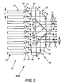
- FIG. 3 is an elevation view schematically illustrating a second embodiment of apparatus in accordance with the present invention including a vertical stack of diode-laser bars, two polarization rotators and a three-element compound prism arranged to half the vertical spacing of output beams of the diode-laser bars.
- FIG. 4 is a three dimensional view schematically illustrating a third embodiment of apparatus in accordance with the present invention including a vertical stack of diode-laser bars, a plurality of polarization rotators and first and second two-element compound prisms arranged to quarter the vertical spacing of output beams of the diode-laser bars.
- FIG. 5 is a plan view schematically illustrating a compound prism arranged to laterally overlap two horizontally spaced parallel beams from a diode-laser bar into a single beam.
- FIG. 6 is a three-dimensional view schematically illustrating a fourth embodiment of apparatus in accordance with the present invention including the apparatus of FIG. 1 arranged to half the vertical spacing of output beams of the diode-laser bars, and a plurality of polarization rotators and the compound prism of FIG. 5 arranged to overlap horizontally spaced output beams having the halved vertical spacing.
- FIG. 7 is a side elevation view schematically illustrating a fifth embodiment of apparatus in accordance with the present invention including two stacks of diode-laser bars having the same spacing therebetween, and a beam combiner including spaced apart reflective strips for combining output beams from the diode-laser bars into a parallel set of beams having a vertical spacing therebetween equal to one-half the spacing of the diode-laser bars.
- FIG. 7A is a side elevation view schematically illustrating apparatus in accordance with the present invention including the beam combiner of FIG. 7 with only one stack of diode-laser bars and a mirror cooperative with the beam combiner for combining output beams from the diode-laser bars into a parallel set of beams having a vertical spacing therebetween equal to one-half the spacing of the diode-laser bars.
- FIG. 7B is a side elevation view schematically illustrating apparatus in accordance with the present invention similar to the apparatus of FIG. 7A but wherein the beam combiner including reflective strips is incorporated in a compound prism.
- FIG. 7C is a side elevation view schematically illustrating apparatus in accordance with the present invention similar to the apparatus of FIG. 7A but wherein the beam combiner including reflective strips is supported on an entrance surface of a slab of transparent material, the slab having a mirror on a portion of a second surface parallel to the first surface.
- FIG. 8 is a front elevation view, seen generally in the direction 8 — 8 of FIG. 7 , schematically illustrating details of the beam combiner of FIG. 7 .
- FIG. 9 is a three-dimensional view schematically illustrating a sixth embodiment of apparatus in accordance with the present invention comprising the apparatus of FIG. 7 , including the two stacks of diode-laser bars having the same spacing therebetween and the beam combiner including spaced apart reflective strips, cooperative with a polarization rotator and the second compound prism of the apparatus of FIG. 4 for combining output beams from the diode-laser bars thereby forming the output beams into a parallel set of beams having a vertical spacing therebetween equal to one-quarter the spacing of the diode-laser bars.
- FIG. 10 is a three-dimensional view schematically illustrating a seventh embodiment of apparatus in accordance with the present invention including the apparatus of FIG. 7 , including the two stacks of diode-laser bars having the same spacing therebetween and the beam combiner including spaced apart reflective strips, cooperative with a polarization rotator and the compound prism of FIG. 5 for combining output beams from the diode-laser bars and overlapping horizontally spaced ones of the combined beams.
- FIG. 11 is a three-dimensional view schematically illustrating an eighth embodiment of apparatus in accordance with the present invention similar to the apparatus of FIG. 6 , but wherein diode-laser bars emit light that is polarized in an orientation at 90° to the polarization orientation of light emitted by the diode-laser bars of FIG. 6 .
- FIG. 12 is a side elevation view schematically illustrating a ninth embodiment of apparatus in accordance with the present invention, similar to the apparatus of claim 3 , but wherein diode-laser bars emit light polarized in a different orientation and the apparatus includes only one polarization rotator.
- FIG. 1 and FIG. 2 schematically illustrate a first embodiment 20 of apparatus in accordance with the present invention.
- Apparatus 20 includes a vertical stack 22 of diode-laser bars 24 .
- Each diode-laser bar includes two diode-lasers (emitters) 26 A and 26 B having emitting apertures 30 A and 30 B respectively.
- Diode-laser bars are shown with only two emitters, here, for convenience of illustration.
- the present invention is equally applicable to diode-laser bars having more than two emitters as well as to a vertical stack of individual emitters.
- corresponding emitters in each diode-laser bar are depicted as being vertically aligned as indicated by dotted line 28 . This should not be construed, however, as limiting the present invention.
- emitters 26 A and 26 B emit beams 32 A and 32 B, respectively, from emitting apertures 30 A and 30 B respectively (see FIG. 2 ).
- Beams here, are depicted by single lines, representing the propagation direction of the beams, for convenience of illustration.
- the diode-laser bars are arranged such that the beams propagate parallel to each other.
- a diode-laser emits a beam that diverges at a half angle of about 35° in a so-called fast-axis and at a half-angle of between about 5° and 15° in a so-called slow-axis direction.
- the fast-axis direction and slow-axis direction are respectively perpendicular and parallel to the length direction of the emitting aperture, i.e., respectively perpendicular and parallel to the length direction of the diode-laser bar.
- the divergence in the slow-axis direction is directly dependent, inter alia, on the width of the diode-laser.
- Each diode-laser bar 24 is provided with a cylindrical lens 34 arranged to collimate beams 32 A and 32 B in the fast-axis direction only. Only two lenses 34 are depicted in FIG. 2 for convenience of illustration.
- Output beams from diode-lasers are plane-polarized.
- the beams may be plane-polarized with the electric vector in the fast-axis direction or the slow-axis direction, depending inter alia, on the method by which the diode-lasers are grown.
- FIGS. 1 and 2 the beams are depicted with the electric vector parallel to the fast-axis direction as indicated by arrows P 1 .
- Diode-laser bars having this polarization orientation are available from Coherent Inc. of Santa Clara, Calif.
- Output beams 32 A and 32 B from diode-laser bar stack 22 have a vertical spacing V corresponding to the vertical spacing of diode-laser bars 24 in the stack.
- the output beams are directed toward a composite prism 36 having a parallelepiped prism component 38 and a triangular prism component 40 .
- Triangular prism 40 has right-angle faces 50 and 51 , and a hypotenuse face 52 .
- Right-angle face 50 serves as an entrance face.
- Hypotenuse face 52 is depicted in FIG. 1 as being at 45° to right-angle faces 50 and 51 but this should not to be construed as limiting the present invention.
- Parallelepiped prism 38 has opposite parallel faces 42 and 44 .
- Parallelepiped prism 38 also has opposite parallel faces 46 and 48 . These faces are inclined at 45° and 135° to faces 42 and 44 . Here again, these angles should not be construed as limiting the present invention. Face 46 is internally reflective for light incident thereon at 45°.
- Face 48 of parallelepiped prism 38 and hypotenuse face 52 of triangular prism 40 are optically bonded together with a highly polarization sensitive (when optically immersed in a medium having the refractive index of the prisms) reflecting coating 54 therebetween.
- Coating 54 may be deposited on either surface 52 or surface 48 . Bonding may be effected using an optical cement or even by optically contacting the surfaces. Bonding these surfaces with the coating provides, in effect, a single internal surface 56 that is highly transmissive, for example greater than 99% transmissive, for radiation incident at 45° plane-polarized in orientation P 1 .
- Surface 56 is highly reflective, for example greater than 99% reflective, for radiation incident at 45° plane-polarized in an orientation P 2 at 90° to orientation P 1 .
- the four beam-pairs polarized in orientation P 2 are reflected from face 46 of parallelepiped prism 38 and then reflected from polarization selective reflecting surface 56 of compound prism 36 . After reflection from surface 56 the P 2 -polarized beams exit compound prism 36 via face 44 of parallelepiped prism component 38 .
- the dimensions of compound prism 36 are selected, cooperative with the angles at which component prism faces are inclined, such that each P 2 -polarized beam leaves the compound prism parallel to and midway between two P 1 -polarized beams. This reduces the vertical spacing between pairs of beams leaving compound prism 36 to a value V/2, i.e., one-half the spacing of corresponding beam-pairs leaving diode-laser bars 24 in stack 22 thereof.
- V/2 spacing of beam pairs is effected by making the vertical spacing between faces 46 and 48 (the height of face 42 ) of parallelepiped prism component 38 equal to nV plus V/2, where n is equal to the number of bars in the upper group.
- a second embodiment 20 A of apparatus in accordance with the present invention includes a stack 22 of diode-laser bars 24 configured as discussed above with respect to FIGS. 1 and 2 .
- Apparatus 20 A includes a compound prism 60 including two parallelepiped prism components 62 and 63 , and a truncated, isosceles, triangular prism component 66 .
- Triangular prism 66 has a base face 68 and isosceles faces 70 and 72 .
- Base face 68 serves as an entrance face.
- Isosceles faces 70 and 72 are depicted in FIG. 3 as being at 90° to each other but this should not be construed as limiting the present invention.
- Truncation face 73 is depicted in FIG. 3 as being parallel to base face 69 but this should also not be construed as limiting the present invention.
- Parallelepiped prism 62 has opposite parallel faces 74 and 76
- parallelepiped prism 63 has corresponding opposite parallel faces 75 and 77 . These faces are transmissive and serve, in each case, as respectively entrance and exit faces.
- Parallelepiped prism 62 also has opposite parallel faces 78 and 80
- parallelepiped prism 63 has corresponding opposite parallel faces 79 and 81 .
- Faces 78 and 80 of parallelepiped prism 62 are inclined at 45° and 135° to faces 74 and 76 .
- Faces 79 and 81 of parallelepiped prism 63 are inclined at 45° and 135° to faces 75 and 77 .
- these angles should not be construed as limiting the present invention.
- Face 78 of parallelepiped prism 62 and face 79 of parallelepiped prism 63 are each internally reflective for light incident thereon at 45°.
- Face 80 of parallelepiped prism 62 and isosceles face 70 of triangular prism 66 are optically bonded together, and face 81 of parallelepiped prism 63 and isosceles face 72 of triangular prism 66 are also optically bonded together.
- These prism faces are bonded together, in each case, with a highly polarization sensitive coating 54 therebetween, as discussed above with respect to compound prism 36 of FIG. 1 . Bonding these surfaces with the coating provides in effect two single internal surfaces 84 and 86 that are each highly transmissive for radiation incident thereon at 45°, plane-polarized in orientation P 1 , and highly reflective, for radiation incident thereon at 45°, plane-polarized in an orientation P 2 .
- Five beam pairs 32 (actually beam pairs 32 A and 32 B as seen in FIG. 2 ) polarized in orientation P 1 enter compound prism 60 through base face 68 of triangular prism component 66 of the compound prism. Two of these five pairs of beams are transmitted through polarization selective reflecting surface 84 , and exit the compound prism via face 76 of parallelepiped prism 62 of the compound prism. One of these five pairs of beams exits the compound prism via truncation face 73 of triangular prism 66 of the compound prism. Another two of these five pairs of beams are transmitted through polarization selective reflecting surface 86 , and exit the compound prism via face 77 of parallelepiped prism 63 of the compound prism.
- Two pairs 32 A and 32 B of beams polarized in orientation P 1 are transmitted through a half-wave plate 88 (polarization rotator), which rotates the plane of polarization of the beams by 90° into orientation P 2 .
- the two beam-pairs polarized in orientation P 2 are reflected from face 78 of parallelepiped prism 62 and then reflected from polarization selective reflecting surface 84 of compound prism 60 . After reflection from surface 84 the P 2 -polarized beams exit compound prism 60 via face 76 of parallelepiped prism 62 of the compound prism.
- Another two pairs 32 A and 32 B of beams polarized in orientation P 1 are transmitted through a half-wave plate 90 , which rotates the plane of polarization of the beams by 90° into orientation P 2 .
- These two pairs of beams undergo reflections at face 79 of parallelepiped prism 63 and surface 86 of the compound prism, exiting the compound prism via face 77 of parallelepiped prism 63 .
- compound prism 60 The dimensions of compound prism 60 are selected, cooperative with the angles at which component prism faces are inclined, such that each P 2 -polarized beam leaves the compound prism parallel to and midway between two P 1 -polarized beams. This reduces the vertical spacing between pairs of beams leaving compound prism 36 to a value V/2, i.e., one-half the spacing of corresponding beam-pairs leaving diode-laser bars 24 in stack 22 thereof. This is the same result as is achieved by above described apparatus 20 of FIG. 1 .
- An advantage of apparatus 20 A compared with apparatus 20 is that beams traverse a shorter path in compound prism 60 than in compound prism 36 . This can be of advantage in limiting beam width due to divergence in the slow-axis.
- a disadvantage of apparatus 20 A compared with apparatus 20 is that compound prism 60 is more complex than compound prism 36 and, accordingly, may be more expensive to manufacture.
- a third embodiment 21 of apparatus in accordance with the present invention is arranged to reduce the vertical spacing of beams emitted by a vertical stack of diode-laser bars by a factor of four.
- Apparatus 21 includes a stack 22 of diode-laser bars 24 , cylindrical lenses 134 , a half-wave plate polarization rotator 58 and a compound prism 36 cooperatively arranged to provide nine pairs 32 A and 32 B of parallel beams having a vertical spacing equal to one-half of the spacing of the diode-laser bars in stack 22 thereof, as described above with reference to apparatus 20 of FIGS. 1 and 2 .
- Polarization rotators 94 are arranged spaced apart and parallel to each other, adjacent to or bonded to face 44 of parallelepiped prism 38 of compound prism 36 .
- Polarization rotators 94 are arranged to intercept only those pairs of beams polarized in orientation P 2 and rotate the polarization of those pairs of beams to orientation P 1 .
- Beam-pairs already polarized in orientation P 1 pass between polarization rotators 94 with polarization orientation unchanged. As a result nine parallel beam-pairs are produced, all polarized in orientation P 1 , with a vertical spacing therebetween of V/2, half the vertical spacing V of diode-laser bars 24 in stack 22 .
- the nine parallel beam-pairs are directed toward another compound prism 36 A, including a parallelepiped prism component 38 A and a triangular prism component 40 A.
- Compound prism 36 A is configured similarly to above described compound prism 36 , with an exception that dimensions of certain features compound prism 36 A are only one-half the dimensions of corresponding features of compound prism 36 . Similar features of the two compound prisms are designated by like reference numerals with the features of compound prism 36 A identified by a suffix A.
- exit face 44 A of compound prism 36 A corresponds to exit face 44 of compound prism 36
- reflective face 46 A of compound prism 36 A corresponds to reflective face 46 of compound prism 36
- Prism components 38 A and 40 A are bonded together with an optical coating to provide an internal, polarization selective reflective surface 56 A.
- the vertical spacing of output of beams from a vertical stack of diode-laser bars is reduced for increasing the intensity of beams as a group.
- Beam intensity or brightness may also be increased by overlapping horizontally spaced ones of the beams emitted by the diode-laser bar stack as depicted in FIG. 5 .
- a polarization rotator 96 and a compound prism 98 are arranged to effect such a lateral overlap of beams 32 A and 32 B having polarization orientation P 1 .
- Compound prism 98 has a parallelepiped prism component 100 and a triangular prism component 102 .
- Triangular prism 102 has right-angle faces 112 and 114 , and a hypotenuse face 116 .
- Hypotenuse face 116 is depicted in FIG. 1 as being at 45° to right-angle faces 112 and 114 but this should not be construed as limiting the present invention.
- Parallelepiped prism 100 has opposite parallel faces 104 and 106 . These faces are transmissive and serve as respectively entrance and exit faces of the compound prism.
- Parallelepiped prism 100 also has opposite parallel faces 108 and 110 . These faces are inclined at 45° and 135° to faces 104 and 106 . Here again, these angles should not be construed as limiting the present invention.
- Face 108 is internally reflective for light incident thereon at 45°.
- Face 110 of parallelepiped prism 100 and hypotenuse face 116 of triangular prism 102 are optically bonded together with a highly polarization sensitive reflecting coating 118 therebetween.
- Coating 118 may be deposited on either face 110 or face 116 . Bonding may be effected, for example, by using an optical cement or by optically contacting the surfaces. Bonding these surfaces with the coating provides, in effect, a single internal surface 120 that is highly transmissive for radiation incident at 45° plane-polarized in orientation P 2 . Surface 120 is highly reflective for radiation incident at 45° plane-polarized in orientation P 1 at 90° to orientation P 2 .
- a fourth embodiment 23 of apparatus in accordance with the present invention includes a polarization rotator 58 and a compound prism 36 arranged to half the vertical spacing of pairs 32 A and 32 B of beams emitted by diode-laser bars 24 in a stack 22 thereof as discussed above with reference to FIGS. 1 and 2 . Beam-pairs having the reduced vertical spacing exit face 44 of compound prism 36 .
- Polarization rotators 94 are arranged spaced apart and parallel to each other, adjacent to or bonded to face 44 of parallelepiped prism 38 of compound prism 36 .
- Polarization rotators 94 are configured and arranged as discussed above with reference to apparatus 21 of FIG. 4 to provide nine parallel beam-pairs, all polarized in orientation P 1 , with a vertical spacing therebetween of V/2, half the vertical spacing V of diode-laser bars 24 in stack 22 thereof.
- Each beam 32 B is transmitted by polarization rotator 96 , which rotates the polarization of the beam to orientation P 2 .
- the P 2 -polarized beams are transmitted through polarization selective reflecting surface 120 , and exit compound prism 98 through face 106 .
- Each beam 32 A enters compound prism 98 through face 104 , is sequentially reflected from face 108 and polarization selective reflecting surface 120 and exits compound prism 98 through face 106 .
- Dimensions and angles of the compound prism are selected, here, such that each beam 32 A exits the compound prism along the same path as, i.e., overlapped with, a corresponding beam 32 B.
- This provides a beam 33 having both P 1 and P 2 -polarized components.
- apparatus 21 provides nine parallel vertically spaced beams 33 , each having both P 1 and P 2 -polarized components.
- beam dimensions and angles of compound prism 98 may be selected cooperative with horizontal spacing H such that beams 32 A and 32 B do not overlap on exiting the compound prism, but merely have the horizontal spacing therebetween reduced. Overlapping beams, of course, have horizontal spacing thereof reduced to zero.
- diode-laser bars may include more emitters and thereby emit more beams than diode-laser bars 24 . Diode-laser bars may include as many as fifty emitters.
- a compound prism such as prism 98 could overlap four horizontally spaced beams to provide two compound beams, six horizontally spaced beams to provide three compound beams, and so on.
- An extensive description of beam overlapping using compound prisms such as prism 98 is provided in copending application Ser. No. 10/266,066 filed Oct. 7, 2002, the complete disclosure of which is hereby incorporated by reference.
- a fifth embodiment 130 of apparatus in accordance with the present invention includes two stacks 22 A and 22 B of respectively five and four, diode-laser bars 24 .
- Emitters (not shown) in each stack here, emit parallel pairs of beams polarized in orientation P 1 . Only one beam 32 B from each bar is visible in FIG. 7 .
- the spacing of diode-laser bars 24 in each stack is the same, here equal to V.
- Stack 22 B emits beams in a direction at 90° to the direction of beams emitted by stack 22 A. Beams from each stack are collimated in the fast-axis direction by cylindrical microlenses 34 .
- Beams emitted by each stack are directed toward a beam combiner 132 on a substrate 133 having opposite surfaces 134 and 136 . Beams from each of stacks 22 A and 22 B are incident on beam combiner 132 at 45° to the emission direction of the beams.
- Each of surfaces 134 and 136 preferably includes an antireflection coating (not shown) arranged to provide minimum reflection at the wavelength of the diode-laser beams in the polarization-orientation of the beams, here orientation P 1 .
- Deposited on surface 136 and forming beam combiner 132 are four parallel, elongated reflective strips 138 separated by spaces 140 (see FIG. 8 ). Surface 136 here, defines a beam combiner plane.
- Strips 138 preferably having greater than 99% reflection for the wavelength of the diode-laser beams in the polarization-orientation of the beams. Reflective strips 138 are preferably sufficiently wide to intercept (at 45° incidence) the full height of a collimated beam from a diode-laser bar 24 , and preferably spaced apart sufficient that such a beam can pass (again at 45° incidence) unvignetted through a space 140 .
- Beam combiner 132 is arranged with respect to diode-laser bar stack 22 A such that, of the five beam-pairs emitted by the stack, outermost ones thereof are transmitted through the beam combiner, with one passing under and the other over reflective strips 138 . The remaining three beam-pairs are transmitted through the beam combiner via a corresponding space 140 between the reflective strips.
- Beam combiner 132 is arranged with respect to diode-laser bar stack 22 B such that the four beam-pairs emitted by the stack are intercepted by reflective strips 138 and reflected by the reflective strips parallel to and midway between beams transmitted through the strips. This provides vertically aligned, parallel beams having a vertical spacing V/2 (half the diode-laser bar spacing V) with all beams having the same polarization orientation.
- FIG. 7A schematically illustrates a variation 130 A of apparatus 30 .
- the apparatus includes only one stack 22 of diode-laser bars 24 .
- the apparatus includes a beam combiner 132 A similar to beam combiner 132 but wherein at least one edge 135 thereof is beveled to avoid vignetting output beams from the diode-laser bars. Beams from the diode laser bars to be reflected from reflective strips 138 of the beam combiner are reflected by a mirror 144 onto the beam combiner.
- FIG. 7B schematically illustrates a variation 130 B of apparatus 130 A.
- a beam combiner 132 B is formed at a bonded interface between a parallelpiped prism 38 and a triangular prism 40 forming a compound prism 36 R similar to compound prism 36 of apparatus 20 except for the bonded interface arrangement.
- reflective strips 139 corresponding reflective strips 138 of apparatus 130 A
- Beam combiner 132 B essentially comprises the reflective strips and the transparent adhesive filling spaces 40 therebetween.
- the beam combiner plane is defined by the interface.
- Face 46 of parallelepiped prism directs beams onto the reflective strips by total internal reflection.
- an “enhanced metal” reflective coating including twenty-two layers alternating Al 2 O 3 and ZnSe on a gold layer, with layers optimized in thickness for 45° incidence in the prism material, will provide about 99.9% reflection for P 1 -polarized radiation and 99.99% or greater for P 2 -polarized radiation with prism material (and adhesive) having a refractive index of about 1.52.
- prism material and adhesive
- FIG. 7C schematically illustrates a variation 130 C of apparatus 130 A.
- a beam combiner 132 C comprising parallel, spaced-apart reflective strips 138 is formed on a lower portion of an entrance surface 150 of a slab 152 of a transparent material surface 150 defines the beam combiner plane.
- a reflector 154 is formed on an upper portion of an exit face 156 of slab 52 .
- Surfaces 150 and 156 are parallel to each other and are inclined to the propagation direction of beams 32 B from diode-lasers 24 .
- the angle is depicted as being 45°. This should not, however, be considered as limiting the invention.
- Reflective strips 138 and mirror 154 are arranged and aligned with diode-laser bars 24 such that beams from five of the diode-laser bars enter the slab 152 via surface 150 , proceed directly to surface 156 , and exit the slab via surface 156 . Three of the beams from the five diode-laser bars pass between the strips, and the other two pass around the strips. Beams from four other of the diode laser bars also enter slab 152 via surface 150 . These beams, however, are intercepted by mirror 154 and are reflected thereby onto reflective strips 138 .
- the beams are reflected by reflective strips 138 out of slab 152 via exit face 156 thereof parallel to the beams that have been directly transmitted through the slab without being reflected by mirror 154 .
- the five directly transmitted beams and the four twice-reflected beams leave the slab parallel to each other and spaced apart by a distance V/2.
- An advantage of apparatus 130 , 130 A, 130 B and 130 C compared with other embodiments of the inventive apparatus described above is that the halving of the beam spacing from the diode-laser bar stacks is accomplished without a need to change, even once, the polarization orientation of any of the beams. All of these apparatus are operable independent of the polarization orientation of the beams.
- a disadvantage of apparatus 130 ( FIG. 7 ) is that two diode-laser bar stacks must be provided, and aligning the two diode-laser bar stacks and the beam combiner may prove somewhat more difficult than aligning one diode-laser bar stack with a compound prism such as compound prism 36 of FIGS. 1 and 2 .
- a disadvantage of apparatus 130 a FIG.
- mirror 144 and beam combiner 132 A must be independently aligned. Nevertheless, providing vertically aligned, parallel beams having the same polarization orientation makes any apparatus 130 , 130 A, 130 B, or 130 C convenient to combine with an above-discussed compound prism 36 A for further reducing the vertical spacing of beams, or with an above-discussed compound prism 98 for overlapping horizontally spaced beams. A description of two such combinations is set forth below with reference to FIG. 9 and FIG. 10
- FIG. 9 depicts a sixth embodiment 25 of apparatus in accordance with the present invention.
- Apparatus 25 comprises a beam combining apparatus 130 including a stack 22 A of five two-emitter diode-laser bars 24 , and a stack 22 B of four two-emitter diode-laser bars 24 .
- Each stack has a diode-laser bar spacing V.
- Each diode-laser bar 24 emits a beam-pair including beams 32 A and 32 B polarized in orientation P 1 .
- Beam combiner 132 combines the beam-pairs from the two stacks as discussed above such that nine parallel beam-pairs polarized in orientation P 1 and having a vertical spacing V/2 leave beam combiner 132 .
- the nine beam-pairs are directed to a compound prism 36 A configured as described above with reference to apparatus 21 of FIG. 4 .
- Dimensions and angles of the compound prism are selected such that the P 2 -polarized beam-pairs exit face 44 A midway between and parallel to the P 1 -polarized beam-pairs as depicted.
- This provides nine pairs 32 A and 32 B of parallel beams having a vertical spacing V/4, i.e., one-quarter of the vertical spacing V of the diode-laser bars in stacks 22 A and 22 B thereof.
- FIG. 10 depicts a seventh embodiment 27 of apparatus in accordance with the present invention.
- Apparatus 27 comprises a beam combining apparatus 130 including a stack 22 A of five two-emitter diode-laser bars 24 , a stack 22 B of four two-emitter diode-laser bars 24 , and beam combiner 132 .
- Nine beam-pairs 32 A and 32 B leave the beam combiner and are directed to a compound prism 98 configured as described above with reference to apparatus 23 of FIG. 6 .
- Each beam 32 B is transmitted by polarization rotator 96 , which rotates the polarization of the beam to orientation P 2 .
- the P 2 -polarized beams are transmitted through polarization selective reflecting surface 120 and exit compound prism 98 through face 106 .
- Each beam 32 A enters compound prism 98 through face 104 , is sequentially reflected from face 108 and a polarization selective reflecting surface 120 , and exits compound prism 98 through face 106 .
- Dimensions and angles of the compound prism are selected such that each beam 32 A exits the compound prism along the same path as, i.e., overlapped with, a corresponding beam 32 B.
- This provides a beam 33 having both P 1 and P 2 -polarized components.
- apparatus 27 provides nine parallel, vertically spaced beams 33 , having a vertical spacing V/2, and each having both P 1 and P 2 -polarized components.
- diode-laser bars have been assumed to emit light polarized in an orientation P 1 , wherein the electric vector is parallel to the fast-axis of emitters in the diode-laser bar.
- diode-laser bars that emit light polarized in orientation P 2 (at 90 to orientation P 1 ), wherein the electric vector is parallel to the slow-axis of emitters in the diode-laser bar are also commercially available. All above discussed embodiments, except apparatus 130 of FIG. 7 , would require a minor reconfiguration to accommodate diode-laser bars emitting P 2 -polarized radiation. Such a reconfiguration is discussed below with reference to FIG. 11 .
- FIG. 11 schematically depicts an eighth embodiment 29 of apparatus in accordance with the present invention.
- Apparatus 29 is configured to achieve the same result as the apparatus 23 of FIG. 6 .
- a diode-laser bar stack 22 P including diode-laser bars 24 P emitting radiation polarized in orientation P 2 is substituted for diode-laser bar stack 24 of apparatus 23 wherein diode-laser bars 24 emit radiation polarized in orientation P 1 .
- the different polarization orientation is accommodated by changing the position of polarization rotators with respect to compound prisms, such that apparatus 29 functions as follows.
- polarization rotator 58 Five pairs 32 A and 32 B of beams polarized in orientation P 2 are transmitted through polarization rotator 58 , which rotates the polarization orientation of the beams into orientation P 1 .
- the P 1 -polarized beams enter compound prism 36 through face 50 of triangular prism component 40 of the compound prism, are transmitted through polarization selective reflecting surface 58 , and exit the compound prism via face 44 of parallelepiped prism component 38 of the compound prism.
- Polarization rotators 94 are arranged spaced apart and parallel to each other, adjacent to or bonded to face 44 of parallelepiped prism 38 of compound prism 36 .
- Polarization rotators 94 rotate the polarization of P 1 -polarized beams to orientation P 2 , thereby providing nine parallel beam-pairs, all polarized in orientation P 2 , with a vertical spacing therebetween of V/2.
- the nine P 2 -polarized beam-pairs are then directed to a compound prism 98 .
- each beam 32 A is transmitted by polarization rotator 96 , which rotates the polarization of the beam to orientation P 1 .
- the P 1 -polarized beams then enter compound prism 98 and are sequentially reflected from face 108 and polarization selective reflecting surface 120 and exit compound prism 98 through face 106 .
- Each beam 32 B enters compound prism 98 via face 112 , is transmitted through polarization selective reflecting surface 120 , and exits compound prism 98 through face 106 .
- Dimensions and angles of the compound prism are selected such that each beam 32 A exits the compound prism along the same path as, i.e., overlapped with, a corresponding beam 32 B. This provides nine parallel, vertically spaced beams 33 , each having both P 1 and P 2 -polarized components.
- polarization rotators 94 could be deployed to rotate the polarization of P 2 -polarized beams to P 1 -polarized beams. This would direct nine P 1 -polarized beam-pairs toward compound prism 98 . In this case, it would be necessary to relocate polarization rotator 96 from its position adjacent face 104 of the compound prism to a position adjacent face 112 of the compound prism.
- FIG. 12 schematically illustrates a ninth embodiment 20 P of apparatus in accordance with the present invention.
- Apparatus 20 P is similar to apparatus 20 A of FIG. 3 with an exception that diode-laser bar stack 22 is replaced by a diode-laser bar stack 22 P emitting beams polarized in orientation P 2 as discussed above with reference to FIG. 11 .
- the two polarization rotators 88 and 90 of apparatus 20 A are replaced with a single polarization rotator 89 located adjacent isosceles prism component 66 of compound prism 60 .
- Polarization rotator 89 rotates the polarization orientation of P 2 -polarized beams to orientation P 1 . This allows the polarization-rotated beams to be transmitted by polarization selective surfaces 84 and 86 .
- P 2 -polarized that are not polarization rotated are twice reflected from surfaces 78 and 84 and 79 and 86 .
- diode-laser bars there may be more or less diode-laser bars in a stack with, generally, beams from M diode-laser bars interleaved with beams from N diode laser bars, where M may be equal to N+1 or where M and N may be equal.
Abstract
Description
Claims (28)
Priority Applications (2)
| Application Number | Priority Date | Filing Date | Title |
|---|---|---|---|
| US10/459,281 US7006549B2 (en) | 2003-06-11 | 2003-06-11 | Apparatus for reducing spacing of beams delivered by stacked diode-laser bars |
| PCT/US2004/017998 WO2004112209A1 (en) | 2003-06-11 | 2004-06-07 | Apparatus for reducing spacing of beams delivered by stacked diode-laser bars |
Applications Claiming Priority (1)
| Application Number | Priority Date | Filing Date | Title |
|---|---|---|---|
| US10/459,281 US7006549B2 (en) | 2003-06-11 | 2003-06-11 | Apparatus for reducing spacing of beams delivered by stacked diode-laser bars |
Publications (2)
| Publication Number | Publication Date |
|---|---|
| US20040252743A1 US20040252743A1 (en) | 2004-12-16 |
| US7006549B2 true US7006549B2 (en) | 2006-02-28 |
Family
ID=33510784
Family Applications (1)
| Application Number | Title | Priority Date | Filing Date |
|---|---|---|---|
| US10/459,281 Expired - Lifetime US7006549B2 (en) | 2003-06-11 | 2003-06-11 | Apparatus for reducing spacing of beams delivered by stacked diode-laser bars |
Country Status (2)
| Country | Link |
|---|---|
| US (1) | US7006549B2 (en) |
| WO (1) | WO2004112209A1 (en) |
Cited By (40)
| Publication number | Priority date | Publication date | Assignee | Title |
|---|---|---|---|---|
| US20060280209A1 (en) * | 2005-02-11 | 2006-12-14 | Hans-Georg Treusch | Beam combining methods and devices with high output intensity |
| US20070268571A1 (en) * | 2006-05-20 | 2007-11-22 | Newport Corporation | Multiple emitter coupling devices and methods with beam transform system |
| US20070268572A1 (en) * | 2006-05-20 | 2007-11-22 | Newport Corporation | Multiple emitter coupling devices and methods with beam transform system |
| US20070291373A1 (en) * | 2006-06-15 | 2007-12-20 | Newport Corporation | Coupling devices and methods for laser emitters |
| US20070291813A1 (en) * | 2006-06-15 | 2007-12-20 | Newport Corporation | Coupling devices and methods for stacked laser emitter arrays |
| US20080089371A1 (en) * | 2006-10-11 | 2008-04-17 | Patrick Reichert | Bright light source with two-dimensional array of diode-laser emitters |
| US20080131060A1 (en) * | 2006-10-06 | 2008-06-05 | Yongdan Hu | Apparatus and method of coupling a fiber optic device to a laser |
| US7515346B2 (en) | 2006-07-18 | 2009-04-07 | Coherent, Inc. | High power and high brightness diode-laser array for material processing applications |
| US20090251697A1 (en) * | 2007-12-17 | 2009-10-08 | Serge Cutillas | Laser emitter modules and methods of assembly |
| US20100183039A1 (en) * | 2009-01-21 | 2010-07-22 | Coherent, Inc. | Two-dimensional diode-laser array with broad-band output |
| US20110103056A1 (en) * | 2008-05-08 | 2011-05-05 | Oclaro Photonics Inc. | High brightness diode output methods and devices |
| EP2450737A2 (en) | 2010-11-09 | 2012-05-09 | PowerPhotonic Ltd | Fast-axis collimator array |
| US20120275149A1 (en) * | 2011-04-29 | 2012-11-01 | Delta Electronics, Inc. | Light source apparatus |
| US8427749B2 (en) | 2010-06-30 | 2013-04-23 | Jds Uniphase Corporation | Beam combining light source |
| US8437086B2 (en) | 2010-06-30 | 2013-05-07 | Jds Uniphase Corporation | Beam combining light source |
| US20130162956A1 (en) * | 2011-12-21 | 2013-06-27 | Sanyo Electric Co., Ltd. | Light source apparatus and projection display apparatus |
| US8644357B2 (en) | 2011-01-11 | 2014-02-04 | Ii-Vi Incorporated | High reliability laser emitter modules |
| US9004699B2 (en) | 2011-04-29 | 2015-04-14 | Delta Electronics, Inc. | Light source system for use in a projector and having a first light source array and a second light source array |
| US9166365B2 (en) | 2010-01-22 | 2015-10-20 | Ii-Vi Laser Enterprise Gmbh | Homogenization of far field fiber coupled radiation |
| US20150333483A1 (en) * | 2014-05-16 | 2015-11-19 | Coherent, Inc. | Light-source including a planar array of diode-laser bars |
| US9647416B2 (en) | 2013-12-23 | 2017-05-09 | Lumentum Operations Llc | Bidirectional long cavity semiconductor laser for improved power and efficiency |
| WO2017122611A1 (en) * | 2016-01-14 | 2017-07-20 | 株式会社アマダミヤチ | Laser device |
| US20170351167A1 (en) * | 2016-06-02 | 2017-12-07 | Coretronic Corporation | Projection system and illumination system |
| US20180294623A1 (en) * | 2011-10-11 | 2018-10-11 | Appotronics Corporation Limited | Light source system and laser light source |
| US10170892B2 (en) * | 2015-06-19 | 2019-01-01 | Amada Miyachi Co., Ltd. | Laser unit and laser device |
| US10203593B2 (en) * | 2017-01-27 | 2019-02-12 | Panasonic Intellectual Property Management Co., Ltd. | Light source device having a retardation plate and projection display apparatus including the light source |
| US10562132B2 (en) | 2013-04-29 | 2020-02-18 | Nuburu, Inc. | Applications, methods and systems for materials processing with visible raman laser |
| US10634842B2 (en) | 2017-04-21 | 2020-04-28 | Nuburu, Inc. | Multi-clad optical fiber |
| US10804680B2 (en) | 2017-06-13 | 2020-10-13 | Nuburu, Inc. | Very dense wavelength beam combined laser system |
| US10940562B2 (en) | 2017-01-31 | 2021-03-09 | Nuburu, Inc. | Methods and systems for welding copper using blue laser |
| US10971896B2 (en) | 2013-04-29 | 2021-04-06 | Nuburu, Inc. | Applications, methods and systems for a laser deliver addressable array |
| US11079605B2 (en) * | 2017-11-13 | 2021-08-03 | Samsung Electronics Co., Ltd. | Total internal reflection prism unit, total internal reflection prism assembly including the same and apparatus for forming a line beam including the same |
| US20220072659A1 (en) * | 2016-04-29 | 2022-03-10 | Nuburu, Inc. | Methods and Systems for Reducing Hazardous Byproduct from Welding Metals Using Lasers |
| US11506850B2 (en) * | 2018-12-13 | 2022-11-22 | Sony Group Corporation | Optical connector, optical cable, and electronic device |
| US11612957B2 (en) * | 2016-04-29 | 2023-03-28 | Nuburu, Inc. | Methods and systems for welding copper and other metals using blue lasers |
| US11624860B2 (en) * | 2019-12-05 | 2023-04-11 | Honda Motor Co., Ltd. | Light body |
| US20230112027A1 (en) * | 2020-07-13 | 2023-04-13 | Focuslight Technologies Inc. | Laser Device |
| US11646549B2 (en) | 2014-08-27 | 2023-05-09 | Nuburu, Inc. | Multi kW class blue laser system |
| US11862927B2 (en) | 2019-02-02 | 2024-01-02 | Nuburu, Inc. | High reliability high power high brightness blue laser diode systems and methods of making the same |
| US11870203B2 (en) | 2018-11-23 | 2024-01-09 | Nuburu, Inc. | Multi-wavelength visible laser source |
Families Citing this family (27)
| Publication number | Priority date | Publication date | Assignee | Title |
|---|---|---|---|---|
| JP4264231B2 (en) * | 2002-08-07 | 2009-05-13 | 浜松ホトニクス株式会社 | Concentrator |
| JP4040934B2 (en) * | 2002-08-30 | 2008-01-30 | 浜松ホトニクス株式会社 | Concentrator |
| US6993059B2 (en) * | 2003-06-11 | 2006-01-31 | Coherent, Inc. | Apparatus for reducing spacing of beams delivered by stacked diode-laser bars |
| DE102004040107A1 (en) * | 2004-08-18 | 2006-02-23 | Arctos Showlasertechnik E.Kfm. | Laser device for generating red laser beam e.g. in advertising and animation etc, uses first and second laser part-beam devices |
| US20070024959A1 (en) * | 2005-07-26 | 2007-02-01 | Infocus Corporation | Laser combiner |
| JP5141080B2 (en) * | 2007-04-10 | 2013-02-13 | セイコーエプソン株式会社 | LIGHT SOURCE DEVICE, IMAGE DISPLAY DEVICE, MONITOR DEVICE, AND LIGHTING DEVICE USING THE SAME |
| US7936799B2 (en) * | 2008-10-27 | 2011-05-03 | Trumpf Photonics Inc. | Interleaving laser beams |
| US8345724B2 (en) * | 2008-10-27 | 2013-01-01 | Trumpf Photonics Inc. | Laser beam interleaving |
| WO2010084021A1 (en) * | 2009-01-23 | 2010-07-29 | Limo Patentverwaltung Gmbh & Co. Kg | Method and device for illuminating a working plane with laser light in a geometrically dense manner |
| US8848753B2 (en) * | 2011-01-20 | 2014-09-30 | Dilas Diode Laser Inc. | Spatially combined laser assembly and method of combining laser beams |
| DE102014205450A1 (en) * | 2014-03-24 | 2015-09-24 | Osram Gmbh | Light source arrangement |
| CN103944068B (en) * | 2014-05-09 | 2017-02-01 | 西安炬光科技有限公司 | Beam combining device for high-power semiconductor laser |
| CN103944066B (en) * | 2014-05-09 | 2018-03-16 | 西安炬光科技有限公司 | A kind of high-power semiconductor laser closes Shu Fangfa |
| CN103944069A (en) * | 2014-05-09 | 2014-07-23 | 西安炬光科技有限公司 | High-power semiconductor laser beam combining device |
| FR3024555A1 (en) * | 2014-07-31 | 2016-02-05 | Valeo Vision | PIXELLIZED LIGHTING MODULE USING A SHUTTER-BASED RECOMBINANT SUBSYSTEM |
| RU2719337C2 (en) * | 2015-07-15 | 2020-04-17 | Нубуру, Инк. | Applications, methods and systems for delivering laser radiation of addressed matrix |
| US10541509B2 (en) * | 2016-01-28 | 2020-01-21 | Sony Corporation | Semiconductor light emitting device |
| CN105846308A (en) * | 2016-05-31 | 2016-08-10 | 南京理工大学 | Spectrum synthesis device and method based on 45-degree incident dichroscope |
| CN106292145A (en) * | 2016-09-07 | 2017-01-04 | 广景视睿科技(深圳)有限公司 | A kind of laser array device and scialyscope illumination path thereof |
| JP2018124538A (en) * | 2017-01-27 | 2018-08-09 | パナソニックIpマネジメント株式会社 | Light source device and projection type display device |
| US10698227B2 (en) * | 2017-08-11 | 2020-06-30 | Christie Digital Systems Usa, Inc. | Apparatus for combining laser beams |
| CN108873128B (en) * | 2018-09-05 | 2024-02-23 | 四川新易盛通信技术有限公司 | Prism, method for using prism as light beam adjuster, prism set and light assembly |
| US11086058B2 (en) | 2018-12-06 | 2021-08-10 | Beijing Voyager Technology Co., Ltd | Transmitter having a light modulator for light detection and ranging (LIDAR) |
| CN109638649B (en) * | 2019-01-14 | 2020-11-03 | 北京工业大学 | High-power semiconductor stacked array space beam combination method and device |
| CN112782860A (en) * | 2019-11-01 | 2021-05-11 | 广州光联电子科技有限公司 | Light source system |
| KR20220086656A (en) * | 2019-11-29 | 2022-06-23 | 사이머 엘엘씨 | Apparatus and method for combining a plurality of laser beams |
| CN114077138A (en) * | 2020-08-21 | 2022-02-22 | 深圳光峰科技股份有限公司 | Light source system |
Citations (28)
| Publication number | Priority date | Publication date | Assignee | Title |
|---|---|---|---|---|
| US4978197A (en) | 1988-08-26 | 1990-12-18 | Fuji Photo Film Co., Ltd. | Beam-combining laser beam source device |
| US5155623A (en) | 1988-09-23 | 1992-10-13 | At&T Bell Laboratories | Arrangement for imaging multiple arrays of light beams |
| US5258989A (en) | 1990-02-12 | 1993-11-02 | Diomed Limited | Solid state laser diode light source |
| US5513201A (en) | 1993-04-30 | 1996-04-30 | Nippon Steel Corporation | Optical path rotating device used with linear array laser diode and laser apparatus applied therewith |
| US5650873A (en) | 1995-01-30 | 1997-07-22 | Lockheed Missiles & Space Company, Inc. | Micropolarization apparatus |
| US5798877A (en) | 1994-07-12 | 1998-08-25 | Coherent, Inc. | Optical system for improving the symmetry of the beam emitted from a broad area laser diode |
| WO1999035724A1 (en) | 1998-01-09 | 1999-07-15 | Jenoptik Aktiengesellschaft | Optical system for symmetrizing the beam of one or more superimposed high-power diode laser |
| US5946130A (en) * | 1997-10-03 | 1999-08-31 | Mcdonnell Douglas Corporation | Optical fiber amplifier network having a coherently combined output and high-power laser amplifier containing same |
| US6005717A (en) | 1998-11-17 | 1999-12-21 | Ceramoptec Industries, Inc. | Diode laser beam combiner system |
| EP0984312A2 (en) | 1998-09-02 | 2000-03-08 | Laserline Gesellschaft für Entwicklung und Vertrieb von Diodenlasern GmbH | Laser diode assembly |
| US6064528A (en) | 1998-11-20 | 2000-05-16 | Eastman Kodak Company | Multiple laser array sources combined for use in a laser printer |
| DE20010309U1 (en) | 1999-06-14 | 2000-09-28 | Fraunhofer Ges Forschung | Diode laser arrangement |
| WO2000057229A1 (en) | 1999-03-23 | 2000-09-28 | Iridex Corporation | Direct diode laser with fiber delivery |
| WO2000060399A1 (en) | 1999-03-31 | 2000-10-12 | Fraunhofer-Gesellschaft zur Förderung der angewandten Forschung e.V. | Optical arrangement for symmetrizing the radiation of two-dimensional arrays of laser diodes |
| US6151342A (en) | 1997-12-08 | 2000-11-21 | Coherent, Inc. | Bright diode-laser light-source |
| US6212216B1 (en) | 1996-12-17 | 2001-04-03 | Ramadas M. R. Pillai | External cavity micro laser apparatus |
| WO2001027686A1 (en) | 1999-10-11 | 2001-04-19 | Unique-M.O.D.E. Ag | Device for symmetrizing the radiation emitted by linear optical transmitters |
| US6229831B1 (en) | 1997-12-08 | 2001-05-08 | Coherent, Inc. | Bright diode-laser light-source |
| EP1143584A2 (en) | 2000-03-31 | 2001-10-10 | Matsushita Electric Industrial Co., Ltd. | Semiconductor laser array |
| US6356577B1 (en) * | 1999-07-15 | 2002-03-12 | Silicon Light Machines | Method and apparatus for combining light output from multiple laser diode bars |
| JP2002148562A (en) | 2000-11-14 | 2002-05-22 | Matsushita Electric Ind Co Ltd | Semiconductor laser machining device |
| US6411323B1 (en) | 1996-10-22 | 2002-06-25 | Sdl, Inc. | High power marking system achieved through power scaling via multiplexing |
| DE10113019A1 (en) | 2001-03-17 | 2002-09-19 | Lissotschenko Vitalij | Beam shaper has boundary surface at which sub-beams are incident from different directions; one sub-beam passes through surface, the other is reflected to combine beams |
| US6556352B2 (en) | 2000-08-23 | 2003-04-29 | Apollo Instruments Inc. | Optical coupling system |
| US20040067016A1 (en) | 2002-10-07 | 2004-04-08 | Anikitchev Serguei G. | Method and apparatus for coupling radiation from a stack of diode-laser bars into a single-core optical fiber |
| US20040091013A1 (en) | 2001-03-30 | 2004-05-13 | Satoshi Yamaguchi | Semiconductor laser device and solid laser device using the same |
| US6785440B1 (en) | 1992-04-16 | 2004-08-31 | Coherent, Inc. | Assembly for focusing and coupling the radiation produced by a semiconductor laser into optical fibers |
| US6851610B2 (en) | 1999-06-07 | 2005-02-08 | Metrologic Instruments, Inc. | Tunnel-type package identification system having a remote image keying station with an ethernet-over-fiber-optic data communication link |
-
2003
- 2003-06-11 US US10/459,281 patent/US7006549B2/en not_active Expired - Lifetime
-
2004
- 2004-06-07 WO PCT/US2004/017998 patent/WO2004112209A1/en active Application Filing
Patent Citations (33)
| Publication number | Priority date | Publication date | Assignee | Title |
|---|---|---|---|---|
| US4978197A (en) | 1988-08-26 | 1990-12-18 | Fuji Photo Film Co., Ltd. | Beam-combining laser beam source device |
| US5155623A (en) | 1988-09-23 | 1992-10-13 | At&T Bell Laboratories | Arrangement for imaging multiple arrays of light beams |
| US5258989A (en) | 1990-02-12 | 1993-11-02 | Diomed Limited | Solid state laser diode light source |
| US6785440B1 (en) | 1992-04-16 | 2004-08-31 | Coherent, Inc. | Assembly for focusing and coupling the radiation produced by a semiconductor laser into optical fibers |
| US5513201A (en) | 1993-04-30 | 1996-04-30 | Nippon Steel Corporation | Optical path rotating device used with linear array laser diode and laser apparatus applied therewith |
| US5798877A (en) | 1994-07-12 | 1998-08-25 | Coherent, Inc. | Optical system for improving the symmetry of the beam emitted from a broad area laser diode |
| US5650873A (en) | 1995-01-30 | 1997-07-22 | Lockheed Missiles & Space Company, Inc. | Micropolarization apparatus |
| US6411323B1 (en) | 1996-10-22 | 2002-06-25 | Sdl, Inc. | High power marking system achieved through power scaling via multiplexing |
| US6212216B1 (en) | 1996-12-17 | 2001-04-03 | Ramadas M. R. Pillai | External cavity micro laser apparatus |
| US5946130A (en) * | 1997-10-03 | 1999-08-31 | Mcdonnell Douglas Corporation | Optical fiber amplifier network having a coherently combined output and high-power laser amplifier containing same |
| US6229831B1 (en) | 1997-12-08 | 2001-05-08 | Coherent, Inc. | Bright diode-laser light-source |
| US6151342A (en) | 1997-12-08 | 2000-11-21 | Coherent, Inc. | Bright diode-laser light-source |
| WO1999035724A1 (en) | 1998-01-09 | 1999-07-15 | Jenoptik Aktiengesellschaft | Optical system for symmetrizing the beam of one or more superimposed high-power diode laser |
| US6337873B1 (en) | 1998-01-09 | 2002-01-08 | Jenoptik Aktiengesellschaft | Optical arrangement for balancing the beam of one or more high power diode lasers arranged one above another |
| EP0984312A2 (en) | 1998-09-02 | 2000-03-08 | Laserline Gesellschaft für Entwicklung und Vertrieb von Diodenlasern GmbH | Laser diode assembly |
| US6175452B1 (en) | 1998-09-02 | 2001-01-16 | Laserline Gesellschaft Fur Entwicklung Und Vertrieb Von Diodenlasem Mbh | Optical arrangement for use in a laser diode arrangement |
| US6005717A (en) | 1998-11-17 | 1999-12-21 | Ceramoptec Industries, Inc. | Diode laser beam combiner system |
| US6064528A (en) | 1998-11-20 | 2000-05-16 | Eastman Kodak Company | Multiple laser array sources combined for use in a laser printer |
| WO2000057229A1 (en) | 1999-03-23 | 2000-09-28 | Iridex Corporation | Direct diode laser with fiber delivery |
| US6683727B1 (en) | 1999-03-31 | 2004-01-27 | Fraunhofer-Gesellschaft Zur Foerderung Der Angewandten Forschung E.V. | Optical arrangement for symmetrizing the radiation of two-dimensional arrays of laser diodes |
| WO2000060399A1 (en) | 1999-03-31 | 2000-10-12 | Fraunhofer-Gesellschaft zur Förderung der angewandten Forschung e.V. | Optical arrangement for symmetrizing the radiation of two-dimensional arrays of laser diodes |
| US6851610B2 (en) | 1999-06-07 | 2005-02-08 | Metrologic Instruments, Inc. | Tunnel-type package identification system having a remote image keying station with an ethernet-over-fiber-optic data communication link |
| DE20010309U1 (en) | 1999-06-14 | 2000-09-28 | Fraunhofer Ges Forschung | Diode laser arrangement |
| US6356577B1 (en) * | 1999-07-15 | 2002-03-12 | Silicon Light Machines | Method and apparatus for combining light output from multiple laser diode bars |
| WO2001027686A1 (en) | 1999-10-11 | 2001-04-19 | Unique-M.O.D.E. Ag | Device for symmetrizing the radiation emitted by linear optical transmitters |
| US6680800B1 (en) | 1999-10-11 | 2004-01-20 | Unique-M.O.D.E. Ag | Device for symmetrizing the radiation emitted by linear optical transmitters |
| EP1143584A2 (en) | 2000-03-31 | 2001-10-10 | Matsushita Electric Industrial Co., Ltd. | Semiconductor laser array |
| US6556352B2 (en) | 2000-08-23 | 2003-04-29 | Apollo Instruments Inc. | Optical coupling system |
| JP2002148562A (en) | 2000-11-14 | 2002-05-22 | Matsushita Electric Ind Co Ltd | Semiconductor laser machining device |
| US20040091209A1 (en) | 2001-03-17 | 2004-05-13 | Alexei Mikhailov | Beam shaping device, system for launching a light beam into an optical fibber, and beam rotation unit for such a beam shaping device or such a system |
| DE10113019A1 (en) | 2001-03-17 | 2002-09-19 | Lissotschenko Vitalij | Beam shaper has boundary surface at which sub-beams are incident from different directions; one sub-beam passes through surface, the other is reflected to combine beams |
| US20040091013A1 (en) | 2001-03-30 | 2004-05-13 | Satoshi Yamaguchi | Semiconductor laser device and solid laser device using the same |
| US20040067016A1 (en) | 2002-10-07 | 2004-04-08 | Anikitchev Serguei G. | Method and apparatus for coupling radiation from a stack of diode-laser bars into a single-core optical fiber |
Non-Patent Citations (3)
| Title |
|---|
| "Uniform Line Illumination with Small Area High Radiant Sources," IBM Technical Disclosure Bulletin, vol. 35, No. 3, Aug. 1992, 2 pages in length. |
| J.D. Minelly et al., "Diode-Array Pumping of Er<SUP>3+</SUP>/Yb<SUP>3+</SUP> Co-Doped Fiber Lasers and Amplifiers," IEEE Photonics Technology Letters, vol. 5, No. 3, Mar. 1993, pp. 301-303. |
| U.S. Appl. No. 10/266,066, filed Oct. 7, 2002, by Serguei Anikitchev and Mathew Rekow, entitled: Method and Apparatus for Coupling Radiation from a Stack of Diode-Laser Bars into a Single-Core Optical Fiber, 53 pages in length. |
Cited By (56)
| Publication number | Priority date | Publication date | Assignee | Title |
|---|---|---|---|---|
| US20060280209A1 (en) * | 2005-02-11 | 2006-12-14 | Hans-Georg Treusch | Beam combining methods and devices with high output intensity |
| US20070268571A1 (en) * | 2006-05-20 | 2007-11-22 | Newport Corporation | Multiple emitter coupling devices and methods with beam transform system |
| US20070268572A1 (en) * | 2006-05-20 | 2007-11-22 | Newport Corporation | Multiple emitter coupling devices and methods with beam transform system |
| US7830608B2 (en) | 2006-05-20 | 2010-11-09 | Oclaro Photonics, Inc. | Multiple emitter coupling devices and methods with beam transform system |
| US7680170B2 (en) * | 2006-06-15 | 2010-03-16 | Oclaro Photonics, Inc. | Coupling devices and methods for stacked laser emitter arrays |
| US20070291373A1 (en) * | 2006-06-15 | 2007-12-20 | Newport Corporation | Coupling devices and methods for laser emitters |
| US20070291813A1 (en) * | 2006-06-15 | 2007-12-20 | Newport Corporation | Coupling devices and methods for stacked laser emitter arrays |
| US7515346B2 (en) | 2006-07-18 | 2009-04-07 | Coherent, Inc. | High power and high brightness diode-laser array for material processing applications |
| US20090190218A1 (en) * | 2006-07-18 | 2009-07-30 | Govorkov Sergei V | High power and high brightness diode-laser array for material processing applications |
| US7697207B2 (en) | 2006-07-18 | 2010-04-13 | Coherent, Inc. | High power and high brightness diode-laser array for material processing applications |
| US7866897B2 (en) | 2006-10-06 | 2011-01-11 | Oclaro Photonics, Inc. | Apparatus and method of coupling a fiber optic device to a laser |
| US20080131060A1 (en) * | 2006-10-06 | 2008-06-05 | Yongdan Hu | Apparatus and method of coupling a fiber optic device to a laser |
| US20080089371A1 (en) * | 2006-10-11 | 2008-04-17 | Patrick Reichert | Bright light source with two-dimensional array of diode-laser emitters |
| US8553737B2 (en) | 2007-12-17 | 2013-10-08 | Oclaro Photonics, Inc. | Laser emitter modules and methods of assembly |
| US20090251697A1 (en) * | 2007-12-17 | 2009-10-08 | Serge Cutillas | Laser emitter modules and methods of assembly |
| US9341856B2 (en) | 2008-05-08 | 2016-05-17 | Ii-Vi Laser Enterprise Gmbh | High brightness diode output methods and devices |
| US20110103056A1 (en) * | 2008-05-08 | 2011-05-05 | Oclaro Photonics Inc. | High brightness diode output methods and devices |
| US8804246B2 (en) | 2008-05-08 | 2014-08-12 | Ii-Vi Laser Enterprise Gmbh | High brightness diode output methods and devices |
| US20100183039A1 (en) * | 2009-01-21 | 2010-07-22 | Coherent, Inc. | Two-dimensional diode-laser array with broad-band output |
| US8160115B2 (en) | 2009-01-21 | 2012-04-17 | Coherent, Inc. | Two-dimensional diode-laser array with broad-band output |
| US9166365B2 (en) | 2010-01-22 | 2015-10-20 | Ii-Vi Laser Enterprise Gmbh | Homogenization of far field fiber coupled radiation |
| US8427749B2 (en) | 2010-06-30 | 2013-04-23 | Jds Uniphase Corporation | Beam combining light source |
| US8437086B2 (en) | 2010-06-30 | 2013-05-07 | Jds Uniphase Corporation | Beam combining light source |
| EP2450737A2 (en) | 2010-11-09 | 2012-05-09 | PowerPhotonic Ltd | Fast-axis collimator array |
| US8644357B2 (en) | 2011-01-11 | 2014-02-04 | Ii-Vi Incorporated | High reliability laser emitter modules |
| US8752981B2 (en) * | 2011-04-29 | 2014-06-17 | Delta Electronics, Inc. | Light source apparatus |
| US9004699B2 (en) | 2011-04-29 | 2015-04-14 | Delta Electronics, Inc. | Light source system for use in a projector and having a first light source array and a second light source array |
| US20120275149A1 (en) * | 2011-04-29 | 2012-11-01 | Delta Electronics, Inc. | Light source apparatus |
| US10530131B2 (en) * | 2011-10-11 | 2020-01-07 | Appotronics Corporation Limited | Light source system and laser light source |
| US20180294623A1 (en) * | 2011-10-11 | 2018-10-11 | Appotronics Corporation Limited | Light source system and laser light source |
| US9063404B2 (en) * | 2011-12-21 | 2015-06-23 | Panasonic Intellectual Property Management Co., Ltd. | Laser light source and projection device having first and second refractive parallelizing elements |
| US20130162956A1 (en) * | 2011-12-21 | 2013-06-27 | Sanyo Electric Co., Ltd. | Light source apparatus and projection display apparatus |
| US10971896B2 (en) | 2013-04-29 | 2021-04-06 | Nuburu, Inc. | Applications, methods and systems for a laser deliver addressable array |
| US10562132B2 (en) | 2013-04-29 | 2020-02-18 | Nuburu, Inc. | Applications, methods and systems for materials processing with visible raman laser |
| US9647416B2 (en) | 2013-12-23 | 2017-05-09 | Lumentum Operations Llc | Bidirectional long cavity semiconductor laser for improved power and efficiency |
| US10490967B2 (en) | 2013-12-23 | 2019-11-26 | Lumentum Operations Llc | Bidirectional long cavity semiconductor laser for improved power and efficiency |
| US20150333483A1 (en) * | 2014-05-16 | 2015-11-19 | Coherent, Inc. | Light-source including a planar array of diode-laser bars |
| US9377611B2 (en) * | 2014-05-16 | 2016-06-28 | Coherent, Inc. | Light-source including a planar array of diode-laser bars |
| US11646549B2 (en) | 2014-08-27 | 2023-05-09 | Nuburu, Inc. | Multi kW class blue laser system |
| US10170892B2 (en) * | 2015-06-19 | 2019-01-01 | Amada Miyachi Co., Ltd. | Laser unit and laser device |
| WO2017122611A1 (en) * | 2016-01-14 | 2017-07-20 | 株式会社アマダミヤチ | Laser device |
| JPWO2017122611A1 (en) * | 2016-01-14 | 2018-08-09 | 株式会社アマダミヤチ | Laser equipment |
| US11612957B2 (en) * | 2016-04-29 | 2023-03-28 | Nuburu, Inc. | Methods and systems for welding copper and other metals using blue lasers |
| US20220072659A1 (en) * | 2016-04-29 | 2022-03-10 | Nuburu, Inc. | Methods and Systems for Reducing Hazardous Byproduct from Welding Metals Using Lasers |
| US20240058896A1 (en) * | 2016-04-29 | 2024-02-22 | Nuburu, Inc. | Methods and Systems for Welding Copper and Other Metals Using Blue Lasers |
| US20170351167A1 (en) * | 2016-06-02 | 2017-12-07 | Coretronic Corporation | Projection system and illumination system |
| US10203593B2 (en) * | 2017-01-27 | 2019-02-12 | Panasonic Intellectual Property Management Co., Ltd. | Light source device having a retardation plate and projection display apparatus including the light source |
| US10940562B2 (en) | 2017-01-31 | 2021-03-09 | Nuburu, Inc. | Methods and systems for welding copper using blue laser |
| US10634842B2 (en) | 2017-04-21 | 2020-04-28 | Nuburu, Inc. | Multi-clad optical fiber |
| US10804680B2 (en) | 2017-06-13 | 2020-10-13 | Nuburu, Inc. | Very dense wavelength beam combined laser system |
| US11079605B2 (en) * | 2017-11-13 | 2021-08-03 | Samsung Electronics Co., Ltd. | Total internal reflection prism unit, total internal reflection prism assembly including the same and apparatus for forming a line beam including the same |
| US11870203B2 (en) | 2018-11-23 | 2024-01-09 | Nuburu, Inc. | Multi-wavelength visible laser source |
| US11506850B2 (en) * | 2018-12-13 | 2022-11-22 | Sony Group Corporation | Optical connector, optical cable, and electronic device |
| US11862927B2 (en) | 2019-02-02 | 2024-01-02 | Nuburu, Inc. | High reliability high power high brightness blue laser diode systems and methods of making the same |
| US11624860B2 (en) * | 2019-12-05 | 2023-04-11 | Honda Motor Co., Ltd. | Light body |
| US20230112027A1 (en) * | 2020-07-13 | 2023-04-13 | Focuslight Technologies Inc. | Laser Device |
Also Published As
| Publication number | Publication date |
|---|---|
| WO2004112209A1 (en) | 2004-12-23 |
| US20040252743A1 (en) | 2004-12-16 |
Similar Documents
| Publication | Publication Date | Title |
|---|---|---|
| US7006549B2 (en) | Apparatus for reducing spacing of beams delivered by stacked diode-laser bars | |
| US6993059B2 (en) | Apparatus for reducing spacing of beams delivered by stacked diode-laser bars | |
| US7010194B2 (en) | Method and apparatus for coupling radiation from a stack of diode-laser bars into a single-core optical fiber | |
| US20130258469A1 (en) | Spatial beam combining for multiple diode laser elements | |
| JP3649737B2 (en) | Beam guidance formation mechanism from linear laser diode array | |
| CN102089943B (en) | High brightness diode output methods and devices | |
| JP6154965B2 (en) | Laser unit and laser device | |
| US8861082B2 (en) | Method and apparatus for combining laser array light sources | |
| US6680800B1 (en) | Device for symmetrizing the radiation emitted by linear optical transmitters | |
| US6377410B1 (en) | Optical coupling system for a high-power diode-pumped solid state laser | |
| US11726341B2 (en) | Method and system for multispectral beam combiner | |
| US7773653B2 (en) | Diode laser arrangement and associated beam shaping unit | |
| US6700709B1 (en) | Configuration of and method for optical beam shaping of diode laser bars | |
| US9235053B2 (en) | Device and method for beam shaping | |
| US10310280B2 (en) | Offset laser array with beam combining optical element | |
| US8842369B2 (en) | Method and apparatus for combining light sources | |
| US6493148B1 (en) | Increasing laser beam power density | |
| US6765725B1 (en) | Fiber pigtailed high power laser diode module with high brightness | |
| JP2014515565A (en) | Method and apparatus for combining light sources as a pump laser array | |
| KR20220054838A (en) | Optical device having a dichroic beam combiner, optical device for use with a dichroic beam combiner, and method of making the same | |
| US8767304B2 (en) | Beam shaping device for focusing light beams from semiconductor laser | |
| US6943957B2 (en) | Laser light source and an optical system for shaping light from a laser-bar-stack | |
| JPH1039250A (en) | Device for forming flat beam | |
| JP3043718B2 (en) | Laser device and manufacturing method thereof | |
| US6400512B1 (en) | Refractive/reflective optical element multiple beam spacer |
Legal Events
| Date | Code | Title | Description |
|---|---|---|---|
| AS | Assignment |
Owner name: COHERENT, INC., CALIFORNIA Free format text: ASSIGNMENT OF ASSIGNORS INTEREST;ASSIGNORS:ANIKITCHEV, SERGUEI G.;AUSTIN, R. RUSSEL;REEL/FRAME:014412/0051;SIGNING DATES FROM 20030617 TO 20030624 |
|
| STCF | Information on status: patent grant |
Free format text: PATENTED CASE |
|
| FPAY | Fee payment |
Year of fee payment: 4 |
|
| FPAY | Fee payment |
Year of fee payment: 8 |
|
| AS | Assignment |
Owner name: BARCLAYS BANK PLC, AS COLLATERAL AGENT, NEW YORK Free format text: NOTICE OF GRANT OF SECURITY INTEREST IN PATENTS;ASSIGNOR:COHERENT, INC.;REEL/FRAME:040575/0001 Effective date: 20161107 |
|
| FPAY | Fee payment |
Year of fee payment: 12 |
|
| AS | Assignment |
Owner name: JPMORGAN CHASE BANK, N.A., AS COLLATERAL AGENT, NEW YORK Free format text: SECURITY INTEREST;ASSIGNORS:II-VI INCORPORATED;II-VI DELAWARE, INC.;M CUBED TECHNOLOGIES, INC.;AND OTHERS;REEL/FRAME:060562/0254 Effective date: 20220701 Owner name: COHERENT, INC., CALIFORNIA Free format text: PATENT RELEASE AND REASSIGNMENT - RELEASE OF REEL/FRAME 040575/0001;ASSIGNOR:BARCLAYS BANK PLC, AS COLLATERAL AGENT;REEL/FRAME:060562/0650 Effective date: 20220701 |