US7006283B2 - Three-dimensional optical amplifier structure - Google Patents
Three-dimensional optical amplifier structure Download PDFInfo
- Publication number
- US7006283B2 US7006283B2 US11/104,026 US10402605A US7006283B2 US 7006283 B2 US7006283 B2 US 7006283B2 US 10402605 A US10402605 A US 10402605A US 7006283 B2 US7006283 B2 US 7006283B2
- Authority
- US
- United States
- Prior art keywords
- light beam
- medium
- optical
- lens
- optical amplifier
- Prior art date
- Legal status (The legal status is an assumption and is not a legal conclusion. Google has not performed a legal analysis and makes no representation as to the accuracy of the status listed.)
- Expired - Fee Related
Links
Images


Classifications
-
- H—ELECTRICITY
- H01—ELECTRIC ELEMENTS
- H01S—DEVICES USING THE PROCESS OF LIGHT AMPLIFICATION BY STIMULATED EMISSION OF RADIATION [LASER] TO AMPLIFY OR GENERATE LIGHT; DEVICES USING STIMULATED EMISSION OF ELECTROMAGNETIC RADIATION IN WAVE RANGES OTHER THAN OPTICAL
- H01S3/00—Lasers, i.e. devices using stimulated emission of electromagnetic radiation in the infrared, visible or ultraviolet wave range
- H01S3/23—Arrangements of two or more lasers not provided for in groups H01S3/02 - H01S3/22, e.g. tandem arrangements of separate active media
- H01S3/2308—Amplifier arrangements, e.g. MOPA
- H01S3/2325—Multi-pass amplifiers, e.g. regenerative amplifiers
- H01S3/2341—Four pass amplifiers
-
- H—ELECTRICITY
- H01—ELECTRIC ELEMENTS
- H01S—DEVICES USING THE PROCESS OF LIGHT AMPLIFICATION BY STIMULATED EMISSION OF RADIATION [LASER] TO AMPLIFY OR GENERATE LIGHT; DEVICES USING STIMULATED EMISSION OF ELECTROMAGNETIC RADIATION IN WAVE RANGES OTHER THAN OPTICAL
- H01S3/00—Lasers, i.e. devices using stimulated emission of electromagnetic radiation in the infrared, visible or ultraviolet wave range
- H01S3/09—Processes or apparatus for excitation, e.g. pumping
- H01S3/091—Processes or apparatus for excitation, e.g. pumping using optical pumping
- H01S3/094—Processes or apparatus for excitation, e.g. pumping using optical pumping by coherent light
- H01S3/0941—Processes or apparatus for excitation, e.g. pumping using optical pumping by coherent light of a laser diode
- H01S3/09415—Processes or apparatus for excitation, e.g. pumping using optical pumping by coherent light of a laser diode the pumping beam being parallel to the lasing mode of the pumped medium, e.g. end-pumping
-
- H—ELECTRICITY
- H01—ELECTRIC ELEMENTS
- H01S—DEVICES USING THE PROCESS OF LIGHT AMPLIFICATION BY STIMULATED EMISSION OF RADIATION [LASER] TO AMPLIFY OR GENERATE LIGHT; DEVICES USING STIMULATED EMISSION OF ELECTROMAGNETIC RADIATION IN WAVE RANGES OTHER THAN OPTICAL
- H01S3/00—Lasers, i.e. devices using stimulated emission of electromagnetic radiation in the infrared, visible or ultraviolet wave range
- H01S3/005—Optical devices external to the laser cavity, specially adapted for lasers, e.g. for homogenisation of the beam or for manipulating laser pulses, e.g. pulse shaping
-
- H—ELECTRICITY
- H01—ELECTRIC ELEMENTS
- H01S—DEVICES USING THE PROCESS OF LIGHT AMPLIFICATION BY STIMULATED EMISSION OF RADIATION [LASER] TO AMPLIFY OR GENERATE LIGHT; DEVICES USING STIMULATED EMISSION OF ELECTROMAGNETIC RADIATION IN WAVE RANGES OTHER THAN OPTICAL
- H01S3/00—Lasers, i.e. devices using stimulated emission of electromagnetic radiation in the infrared, visible or ultraviolet wave range
- H01S3/05—Construction or shape of optical resonators; Accommodation of active medium therein; Shape of active medium
- H01S3/06—Construction or shape of active medium
- H01S3/0602—Crystal lasers or glass lasers
- H01S3/0604—Crystal lasers or glass lasers in the form of a plate or disc
-
- H—ELECTRICITY
- H01—ELECTRIC ELEMENTS
- H01S—DEVICES USING THE PROCESS OF LIGHT AMPLIFICATION BY STIMULATED EMISSION OF RADIATION [LASER] TO AMPLIFY OR GENERATE LIGHT; DEVICES USING STIMULATED EMISSION OF ELECTROMAGNETIC RADIATION IN WAVE RANGES OTHER THAN OPTICAL
- H01S3/00—Lasers, i.e. devices using stimulated emission of electromagnetic radiation in the infrared, visible or ultraviolet wave range
- H01S3/05—Construction or shape of optical resonators; Accommodation of active medium therein; Shape of active medium
- H01S3/08—Construction or shape of optical resonators or components thereof
- H01S3/08072—Thermal lensing or thermally induced birefringence; Compensation thereof
-
- H—ELECTRICITY
- H01—ELECTRIC ELEMENTS
- H01S—DEVICES USING THE PROCESS OF LIGHT AMPLIFICATION BY STIMULATED EMISSION OF RADIATION [LASER] TO AMPLIFY OR GENERATE LIGHT; DEVICES USING STIMULATED EMISSION OF ELECTROMAGNETIC RADIATION IN WAVE RANGES OTHER THAN OPTICAL
- H01S3/00—Lasers, i.e. devices using stimulated emission of electromagnetic radiation in the infrared, visible or ultraviolet wave range
- H01S3/23—Arrangements of two or more lasers not provided for in groups H01S3/02 - H01S3/22, e.g. tandem arrangements of separate active media
- H01S3/2308—Amplifier arrangements, e.g. MOPA
- H01S3/2325—Multi-pass amplifiers, e.g. regenerative amplifiers
Definitions
- the present invention relates to an optical amplifier, and in particular to a three-dimensional optically pumped amplifier structure for lasers.
- the oscillator is traditionally a mode-locked laser producing very short pulses, typically less than 100 ps, at high frequency, typically a few tens of MHz, and with low energy per pulse, typically a few nJ.
- an amplifier working at a lower repetition rate ranging from a few kHz to a few hundreds of kHz depending on the pumping configuration, is used.
- the traditional systems are complex and complicated to use because they involve active modulation (acousto-optic or electro-optic), high-speed electronics, short-pulse production for the oscillator, and injection and synchronization of the pulses inside the amplifier.
- Passively Q-switched lasers using Nd-doped crystals can produce high peak power pulses of several kW at a wavelength of 1064 nm.
- the pulse width can vary from a few tens of ns (A. Agnesi, S. Dell'Acqua, E. Piccinini, G. Reali and G. Piccinno, “Efficient wavelength conversion with high power passively Q-switched diode-pumped neodymium laser”, IEEE, J. Q. E., Vol. 34, 1480–1484, 1998) to a few hundreds of ps (J. J. Zayhowski, “Diode-pumped passively Q-switched picosecond microchip lasers”, Opt.
- pulses of 19 ns and 108 ⁇ J can be obtained at 25 kHz and 1064 nm from a diode-pumped Nd:YAG laser with a Cr 4+ :YAG saturable absorber crystal.
- the high peak power of these lasers allows efficient wavelength conversion into the ultra-violet (UV) range with optically nonlinear materials (A. Agnesi, S. Dell'Acqua, E. Piccinini, G. Reali and G. Piccinno, “Efficient wavelength conversion with high power passively Q-switched diode-pumped neodymium laser”, IEEE, J. Q. E., Vol.
- a microchip laser combines the two materials in a monolithic crystal (J. J. Zaykowski, “Non linear frequency conversion with passively Q-switched microchip lasers”, CLEO 96, paper CWA6, 23 6–237, 1996) to reduce the energy to approximately 8 ⁇ J at 1064 nm.
- the two materials i.e. the laser material and the saturable absorber, can be connected by thermal bonding, or the saturable absorber can be grown by liquid phase epitaxy (LPE) directly on the laser material (B. Ferrand, B. Chambaz, M.
- Another solution consists of combining a compact oscillator, producing short pulses at high frequency, with an amplifier to increase the pulse energy.
- Amplifiers have been used in the past with pulsed microlasers. After amplification, pulses with 87 nJ (small-signal gain of 3.5) at 100 kHz have been produced using a 10-W diode bar as a pump (C. Larat, M. Schwarz, J. P. Pocholle, G. Feugnet, M. Papuchon, “High repetition rate solid-state laser for space communication”, SPIE, Vol.
- Nd:YAG and Nd:YVO 4 limits the small-signal gain to a value lower than that obtained when only Nd:YVO 4 is used in both the oscillator and the amplifier; the aforementioned spectral distance is comprised between 5.5 cm ⁇ 1 and 7.0 cm ⁇ 1 (J. F. Bernard, E. Mc Cullough, A. J. Alcock, “High gain, diode-pumped Nd:YVO 4 slab amplifier”, Opt. Commun. Vol. 109, 109–114, 1994).
- a high small-signal gain of 240 was achieved in an end-pumped double-pass bulk Nd:YLF amplifier, but it was used with a CW laser with an expensive diode-beam shaping optical setup (G. J. Friel, W. A. Clarkson, D. C. Hanna, “High gain Nd:YLF amplifier end-pumped by a beam shaped bread-stripe diode laser”, CLEO 96, paper CTUL 28, p. 144, 1996).
- Nd:YAG and Nd:YVO 4 allowed the best use of their respective properties: Nd:YAG/Cr 4+ :YAG microchip lasers are simpler and easier to manufacture than Nd:YVO 4 microchips because they use the same crystal (YAG) for the laser medium and the saturable absorber, and can be produced in a collective fashion. In addition they produce shorter pulses except in the case of the semiconductor saturable absorber described in B. Braun, F. X. Kartner, G. Zhang, M. Moser, U. Keller, “56 ps passively Q-switched diode-pumped microchip laser”, Opt. Lett. 22, 381–383, 1997.
- Nd:YVO 4 is on the other hand well suited for amplification due to its high stimulated emission cross section. It is also better suited than Nd:YAG for higher repetition rates due to a shorter fluorescence lifetime (100 ⁇ s instead of 230 ⁇ s).
- the light beam to be amplified initially gets passed through the amplifier medium along a first path and subsequently gets reflected back through the amplifier medium along a second path, thereby traversing the amplifier medium twice.
- the planar geometry used by Georges et at is not optimal since the pump beam propagates in three dimensions whereas the light beam to be amplified travels in a single plane. This results in poor overlap between the volume occupied in the amplifier medium by the pump beam and the volume occupied in the amplifier medium by the light beam to be amplified.
- Georges et al. alludes to multi-pass scenarios wherein the light beam (to be amplified) traverses the amplifier medium at least twice. Such multi-pass amplification schemes are known.
- McIntyre discloses co-linear and two-dimensional multi-pass amplification schemes in U.S. Pat. No. 5,268,787, issued Dec. 7, 1993, which is incorporated herein by reference.
- Plaessmann et al. in U.S. Pat. No. 5,546,222, issued Aug. 13, 1996, which is incorporated herein by reference, discloses a multi-pass laser amplifier that uses optical focusing between subsequent passes through a single gain medium.
- the multi-pass laser amplification schemes disclosed by Plaessman et al. are all two-dimensional schemes, i.e. the multi-paths of the light beam traversing the amplifier medium all lie in a same plane.
- the number of optical components used in the embodiments taught by Plaessman et al. is relatively small and consequently, the alignment of said components is crucial in view of the multi-pass amplification scheme.
- C. LeBlanc et al. “Compact and efficient multi-pass Ti:sapphire system for femto-second chirped-pulse amplification at the terawatt level”, Optics Letters, Vol. 18, No. 2, Pp. 140–142, Jan. 15, 1993, discloses a Ti:sapphire crystal amplifier medium pumped at two ends by Nd:YAG light and traversed eight times by the light beam to be amplified. The light beam to be amplified traverses the amplifier medium four times in a first plane and four other times in a distinct second plane parallel to the first plane.
- Scott et al. “Efficient high-gain laser amplification from a low-gain amplifier by use of self-imaging multi-pass geometry”, Applied Optics, Vol. 40, No. 15, Pp. 2461–2467, 20 May 2001.
- Scott et al. illustrates how the light beam to be amplified traverse the amplifier medium four times in a first plane and four additional times in a distinct other plane parallel to the first plane.
- a phase-conjugate mirror is then used to double the number of passes.
- An object of the invention is to provide a method for amplifying a light beam comprising the step of passing a light beam through an amplifying medium along multiple paths, wherein no more than two of the multiple paths lie in a same plane.
- the present invention relates to an optical amplifier stage for amplifying a light beam comprising:
- Another feature of the present invention relates to an optical amplifier stage for amplifying a light beam comprising:
- the present invention relates to a laser system for emitting a pulsed light beam comprising:
- FIG. 1 is a schematic illustration of a prior art laser system
- FIGS. 2 a and 2 b is a schematic illustration of a prior art optically pumped amplifier structure
- FIG. 3 is a schematic illustration of an embodiment of the present invention.
- FIG. 4 is a cross-sectional view of an amplifier medium of the embodiment of FIG. 3 ;
- FIG. 5 is a schematic illustration of an alternative embodiment of the present invention.
- FIG. 6 is a cross-sectional view of an amplifier medium of the embodiment of FIG. 5 ;
- FIGS. 7 a and 7 b are schematic illustrations of a redirecting means in the form of a recirculating fiber
- FIGS. 8 a and 8 b are schematic illustrations showing the equivalent performance of a roof prism compared to two mirrors
- FIG. 9 is an end view of the embodiment of FIG. 3 with an anisotropic amplifier medium
- FIG. 10 is a plot of horizontal and vertical beam radii vs distance from the lens for the embodiment of FIG. 3 ;
- FIG. 11 is an alternative embodiment of an amplifier according to the present invention.
- FIG. 12 a illustrates the alignment of the crystal in the embodiment of FIG. 3 ;
- FIG. 12 b illustrates the alignment of the crystal in the embodiment of FIG. 11 ;
- FIG. 13 is an end view of the embodiment of FIG. 11 ;
- FIG. 14 is a plot of horizontal and vertical beam radii vs distance from the lens for the embodiment of FIG. 11 ;
- FIG. 15 an alternative embodiment of the present invention with eight passes through the amplifier medium
- FIG. 16 is an end view of the embodiment of FIG. 15 .
- FIG. 1 depicts a conventional entirely passive laser system for both the generation and amplification of short pulses, the full description of which is found in U.S. Pat. No. 6,373,864, issued to Georges et al. on Apr. 16, 2002.
- the Georges et al. laser system comprises a first sub-system; i.e. a microchip laser stage 1 , and a second sub-system; i.e. an amplifier stage 2 .
- a first pump laser 3 emits a first pumping radiation 4 , which is directed by a first lens 5 towards a microchip laser 6 .
- the microchip laser 6 comprises reflective elements, a first gain medium and a saturable absorber, all of which are not depicted.
- a microchip laser beam 8 is directed by lenses 7 and 9 towards an amplifying medium 10 which is optically pumped by a second pump laser 14 , whose pumping radiation 13 is directed towards the amplifying medium 10 by a lens 12 .
- a dichroic filter 11 transparent to pumping radiation 13 and reflective to the microchip laser beam 8 , is disposed at an end of the amplifying medium 10 .
- the pumping radiation 13 generated by pump laser 14 , is transmitted through the dichroic filter 11 and excites the amplifier medium 10 , while the microchip laser beam 8 , traversing the amplifying medium 10 a first time for a first amplification, is reflected by the dichroic filter 11 back through the amplifying medium 10 a second time for a second amplification.
- a twice-amplified microchip laser beam 15 is directed by lens 9 to an optical circuit (not shown).
- FIGS. 2 a and 2 b illustrate the amplifying medium 10 being pumped by the pumping radiation 13 .
- Shaded area 16 depicts a cross-sectional view of the volume being optically pumped by the pumping radiation 13 . It is apparent from FIGS. 2 a and 2 b that the optically pumped volume 16 of the amplifying medium 10 is not being substantially overlapped by the microchip laser beam 8 and the twice-amplified microchip laser beam 15 .
- the present invention addresses the poor overlap situation by disclosing a three-dimensional amplification scheme that sees the beam to be amplified travel along multiple paths inside the amplifier medium with the combined volume occupied by the multiple paths inside the amplifier medium substantially overlapping with the volume occupied by the optical pump beam. This provides a laser system with high gain and good efficiency.
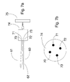
- FIG. 3 depicts a preferred embodiment of the present invention.
- a beam of light to be amplified 20 1 propagates parallel to the optical axis (OA) of a lens 19 and is directed by the lens 19 towards an amplifier medium 22 , which is being optically pumped at a wavelength ⁇ p by a pump beam 23 through a dichroic filter 24 transparent to ⁇ p .
- the beam 20 1 having a wavelength ⁇ 1 , traverses the amplifier medium 22 for a first time along a first path for a first amplification and is reflected by the dichroic filter 24 .
- the reflected beam 20 2 traverses the amplifier medium a second time for a second amplification along a second path and is directed by the lens 19 towards a reflector in the form of a corner cube 30 .
- the corner cube 30 displaces the beam 20 2 into a displaced beam 20 3 and reflects the beam 20 3 back towards the lens 19 , which directs the beam 20 3 along a third path towards the amplifier medium 22 for a third amplification.
- the dichroic filter 24 reflects the beam a second time and the reflected beam 20 4 traverses the amplifier medium for a fourth amplification along a fourth path. Subsequently, the beam 20 4 is directed towards an output port, preferably via the lens 19 .
- FIG. 4 shows a cross-sectional view of the amplifier medium 22 and a pump beam area 23 populated by areas occupied by the light beam to be amplified as it propagates along the first, second, third and fourth paths here labeled by the corresponding beam numerals 20 1 , 20 2 , 20 3 and 20 4 .
- the embodiment just described has the input beam 20 1 and the output beam 20 4 traversing the lens 19 , it is not necessary that they do so for the invention to work.
- FIG. 5 depicts an alternative embodiment of the present invention, in which an output pump beam 34 of a fiber coupled diode array 35 is imaged by a lens 36 on an amplifier medium 37 through a dichroic filter 38 .
- a light beam to be amplified 39 propagates along a first path 40 towards a lens 41 , which directs the beam 39 towards the amplifier medium 37 and the dichroic filter 38 .
- the dichroic filter 38 reflects the light beam 39 back through the amplifier medium 37 and towards the lens 41 , which directs beam 39 along a second path 42 to a first roof prism 43 .
- the roof prism 43 reflects and displaces the beam 39 to propagate along a third path 44 towards the lens 41 , which directs the beam 39 towards the amplifier medium 37 and the dichroic filter 38 .
- the dichroic filter 38 reflects the beam 39 for propagation through the amplifier medium 37 and towards the lens 41 , which directs the beam 39 along a fourth path 45 to a second roof prism 46 .
- the roof prism 46 reflects and displaces the beam 39 to propagate along a fifth path 47 towards the lens 41 , which directs beam 39 through the amplifier medium 37 to the dichroic filter 38 .
- the dichroic filter 38 reflects the beam 39 through the amplifier medium 37 and towards the lens 41 , which directs the beam 39 along a sixth path 50 to a third roof prism 51 .
- the roof prism 51 reflects and displaces the beam 39 to propagate along a seventh path 52 towards the lens 41 , which directs beam 39 through the amplifier medium 37 to dichroic filter 38 .
- the dichroic filter 38 reflects the beam 39 for propagation through the amplifier medium 37 and towards the lens 41 , which directs the beam 39 along an eight path 53 towards an output port (not shown).
- the beam 39 is amplified each time it traverses the amplifier medium 37 and consequently, according to the description just given, is amplified eight times.
- FIG. 6 shows a cross-sectional view of the amplifier medium 37 with a concentric dashed circle 60 representing the area of the cross-section being optically pumped by the pump beam 34 . Also shown in FIG. 6 are the areas of beam 39 traveling along the various paths 40 , 45 , 47 , 53 , 42 , 44 , 50 , and 52 as they intercept the cross-section of the pump beam. One can observe in FIG. 6 that the area covered by beam paths 40 , 45 , 47 , 53 , 42 , 44 , 50 , and 52 substantially overlap the area 60 covered by the pump beam 34 .
- FIG. 7 a illustrates how a recirculating fiber 62 can be used to replace the roof prisms or the corner cube of the previously described embodiments.
- a beam of light 60 propagates towards a lens 74 , intersects the lens 74 at a port 72 and is directed along a first path by the lens 74 towards a reflector 75 .
- the beam 60 is then reflected towards the lens 74 along a second path by the reflector 75 and is directed by the lens 74 towards a first end of a recirculating fiber 61 , said first end located at port 70 .
- the beam 60 propagates through the recirculating fiber 61 and exits the recirculating fiber 61 at port 71 .
- the beam 60 is then directed along a third path by the lens 74 towards the reflector 75 .
- the beam 60 is then reflected towards the lens 74 along a fourth path by the reflector 75 and is directed by the lens 74 towards a port 73 .
- the beam of light 60 then exits the port 73 as an output beam 62 .
- FIG. 7 a is frontal view of the side of the lens 74 having the ports 70 , 71 , 72 and 73 .
- FIGS. 8 a and 8 b show how mirrors can perform the equivalent task of a roof prism.
- FIG. 8 a one can see an optical beam 85 entering a roof prism 80 and being redirected by the roof prism 80 .
- FIG. 8 b shows how the two mirrors 81 and 82 perform the same function as the roof prism 80 on the beam 85 .
- a combination of mirrors can function as a corner cube.
- Nd:YVO 4 Nd:YAG, Yb:YAG, Er:glass and Yb:glass can all be utilized as the amplifier medium.
- an a-cut Neodymium doped Vanadate (Nd:YVO 4 ) crystal is the preferred choice for the amplifier medium, because of a large stimulated cross-section and a strong broadband absorption at 809 nm. Since YVO 4 is an anisotropic crystal, the gain therefrom is polarization dependent, i.e.
- the polarization state of the signal beam must be maintained and aligned parallel with the crystallographic c axes of the crystal during each amplification stage.
- a prism is preferred to a corner cube as a reflector, since a prism can withstand higher power and higher energy beams. Therefore, to maintain the polarization of the signal beam constant, the prism and the YVO 4 crystal must be carefully aligned.
- the YVO 4 crystal is anisotropic, propagation along the crystallographic a-axis exhibits a different thermal conductivity along the crystallographic b-axis (equivalent to a-axis in a uniaxial YVO 4 crystal) than along the crystallographic c-axis (equivalent to an optical axis in a uniaxial YVO 4 crystal). Since the crystal is primarily cooled from the sides, the absorbed pump power creates an anisotropic variation of the indices, which results in an anisotropic thermal lens, i.e. the focal length along the two transverse axes (horizontal and vertical) is different.
- a beam propagating in the amplifier medium 23 will undergo anisotropic focusing during each pass, and become elliptical and astigmatic.
- the beam 20 2 becomes somewhat elliptical, but after four passes the beam 20 4 is clearly much broader along the horizontal axis than the vertical axis.
- the horizontal (or major) axis of the beam corresponding to the b-axis of the crystal 23 and the longitudinal axis of the corner cube 30 , i.e. the direction in which the light travels from one facet of the corner cube 30 to the other.
- the graph in FIG. 10 illustrates the difference in beam radius along the horizontal and vertical axes at distances from the lens 19 .
- the image of the beam is rotated by 90° between each pass, whereby the elliptical focusing acts in perpendicular directions for consecutive passes, i.e. the axis of the beam experiencing more broadening during the first pass will receive less broadening during the second pass, thereby recovering a circular profile.
- this technique requires a ring cavity to enable multiple passes in the gain medium, which, thus far, has prevented its use in amplifiers.
- the astigmatism can be compensated after the beam has exited the amplifier using various combinations of lenses to refocus the elliptical astigmatic beam back into a circular profile.
- lensing solutions require difficult alignment procedures, and vary from laser to laser, because they are very sensitive to variations in the astigmatism.
- compensation does not operate for various power levels, since the thermal lens and the corresponding astigmatism vary with the absorbed pump power.
- FIG. 11 illustrates an alternative embodiment of the present invention, similar to the embodiment of FIG. 3 , in which a lens 119 directs an input beam 120 1 along a first path through an amplifier medium 122 , which is being optically pumped at a wavelength ⁇ p by a pump beam 123 through a dichroic filter 124 transparent to ⁇ p .
- the dichroic filter 124 reflects the input beam 120 1 back through the amplifier medium 122 along a second path forming reflected beam 120 2 .
- a redirecting means preferably in the form of a right angle prism 130 , creates a lateral displacement of the reflecting beam 120 2 and redirects the reflected beam 120 2 back through the amplifier medium 122 along a third path as redirected beam 120 3 , which gets reflected by the dichroic filter 124 forming output beam 120 4 traveling along a fourth path.
- the plane defined by the first and second paths and the plane defined by the third and fourth paths are distinct due to the beam-displacing action of the prism 130 . Having distinct planes implies that the combined volume occupied by the beam paths inside the amplifier medium 122 is greater than it would be were it not for the presence of the prism 130 .
- the prism 130 is defined by a longitudinal (or displacement) axis LA along which the light travels when being displaced, e.g. reflected from total internal reflection (TIR) surface of the prism 130 to another, and a transverse axis TA defined by the intersection of the two TIR planar surfaces.
- TIR total internal reflection
- the c-axis (and/or b-axis) of the crystal is rotated by an acute angle relative to the longitudinal and transverse axes LA and TA, respectively, of the prism 130 , e.g. by 40°to 50°, preferably 45°.
- the beam 120 2 is slightly elliptical with the major and minor axes along diagonal lines, which are at the angle or rotation, e.g.
- FIG. 14 A plot of the beam radii along the major and minor axes according to the embodiment of FIG. 11 is found in FIG. 14 , which when compared to that of FIG. 10 , illustrates that the beam output beam 120 4 is much closer to circular than in the previous embodiment.
- a half-wave plate 132 is positioned in the first path to rotate the polarization of the input beam 120 1 corresponding to the rotation angle of the crystal of the amplifier medium 122 , e.g. by 40° to 50°, preferably 45°, back into alignment with the proper axis, e.g. the c-axis for the YVO 4 example.
- the half-wave plate 132 is positioned in each of the first, second, third and fourth paths, as in FIG. 11 , whereby the polarization of the beams of light 120 1 to 120 4 will continually be rotated between its original state, when incident upon the redirecting means (e.g.
- the redirecting means is a prism
- the polarization of the light beams 120 1 to 120 4 is selected parallel to the longitudinal axis LA of the prism 130 , thereby to avoid depolarization during total internal reflection therein.
- the polarization of the light beams 120 1 to 120 4 will rotate between horizontally polarized on the prism side of the half-wave plate 132 to having a 45° polarization on the amplifier medium side of the half-wave plate 132 .
- the amplifier according to the present invention works independently of the absorbed pump power and of the heat dissipation from the lateral sides of the amplifier medium 122 . Accordingly, the amplifier according to the present invention can be operated at virtually any output power, while preserving optimum beam quality. Moreover, aging of the pump diode will not degrade the roundness of the beam.
- an input beam 220 1 is directed by a lens 219 through an amplifier medium 222 , which is being optically pumped at a wavelength ⁇ p by a pump beam 223 through a dichroic filter 224 transparent to ⁇ 4 .
- a first prism 230 a laterally displaces and redirects a reflected beam 220 2 traveling along a second path through the amplifier medium 222 back along a third path through the amplifier medium 222 forming redirected beam 220 3 .
- second and third prisms 230 b and 230 c redirect beams 220 4 to 220 7 traveling along fourth to seventh paths, respectively through the amplifier medium 222 until the output beam 220 8 is directed out the output port.
- the amplifier medium is comprised of an anisotropic crystal, e.g. Nd:YVO 4 , with its axis rotated at an angle to the longitudinal axes of the first, second and third prisms 230 a to 230 c , respectively, whereby the astigmatism is self compensated during multiple passes therethrough.
- the major and minor axes of the elliptical beams are effectively rotated by 90°, whereby during the next two passes through the amplifier medium 223 the major axis undergoes more focusing than the minor axis, thereby recreating a circular beam profile. Any multiple of four passes through the amplifier medium 223 results in optimum compensation.
Abstract
The present invention relates to a multi-pass three-dimensional amplifier structure in which a beam of light traverses an amplifier medium multiple times via distinct multiple paths. The distribution of the multiple paths being such that the volume occupied by the multiple paths inside the amplifier medium substantially overlaps with the volume of the amplifier medium being optically pumped by an optical pump beam. The distribution of the optical paths is such that no more than two of the multiple paths lie in a same plane. The astigmatism induced by anisotropic amplifying crystals is self-compensated by aligning the crystallographic axes of the amplifying crystal at a 45° angle to the longitudinal axis of the redirecting means.
Description
The present application is a continuation-in-part of U.S. patent application Ser. No. 10/342,437 filed Jan. 13, 2003 now abandoned, which claimed priority from Canadian Patent Application No. 2,368,031 filed Jan. 15, 2002 and from Canadian Patent Application No. 2,370,037 filed Feb. 1, 2002, which are incorporated herein by reference for all purposes. The present application also claims priority from U.S. Patent Application No. 60/649,227 filed Feb. 2, 2005, which is incorporated herein by reference for all purposes.
The present invention relates to an optical amplifier, and in particular to a three-dimensional optically pumped amplifier structure for lasers.
Production of short pulses with high energy per pulse is usually achieved by a combination of one oscillator and one amplifier. The oscillator is traditionally a mode-locked laser producing very short pulses, typically less than 100 ps, at high frequency, typically a few tens of MHz, and with low energy per pulse, typically a few nJ. To increase the pulse energy to several μJ, an amplifier working at a lower repetition rate, ranging from a few kHz to a few hundreds of kHz depending on the pumping configuration, is used. Unfortunately, the traditional systems are complex and complicated to use because they involve active modulation (acousto-optic or electro-optic), high-speed electronics, short-pulse production for the oscillator, and injection and synchronization of the pulses inside the amplifier.
Passively Q-switched lasers using Nd-doped crystals can produce high peak power pulses of several kW at a wavelength of 1064 nm. Depending on the experimental setup, the pulse width can vary from a few tens of ns (A. Agnesi, S. Dell'Acqua, E. Piccinini, G. Reali and G. Piccinno, “Efficient wavelength conversion with high power passively Q-switched diode-pumped neodymium laser”, IEEE, J. Q. E., Vol. 34, 1480–1484, 1998) to a few hundreds of ps (J. J. Zayhowski, “Diode-pumped passively Q-switched picosecond microchip lasers”, Opt. Lett., Vol. 19, 1427–1429, 1994). For example, pulses of 19 ns and 108 μJ can be obtained at 25 kHz and 1064 nm from a diode-pumped Nd:YAG laser with a Cr4+:YAG saturable absorber crystal. The high peak power of these lasers allows efficient wavelength conversion into the ultra-violet (UV) range with optically nonlinear materials (A. Agnesi, S. Dell'Acqua, E. Piccinini, G. Reali and G. Piccinno, “Efficient wavelength conversion with high power passively Q-switched diode-pumped neodymium laser”, IEEE, J. Q. E., Vol. 34, 1480–1484, 1998; J. J. Zayhowski, “Diode-pumped passively Q-switched picosecond microchip lasers”, Opt. Lett., Vol. 19, 1427–1429, 1994; J. J. Zaykowski, “UV generation with passively Q-switched microchip laser”, Opt. Lett., Vol. 21, 588–590, 1996).
To reduce the pulse width, while using the same material combination, one must combine the active medium and the saturable absorber in a short distance to reduce the cavity length to about 1 mm. A microchip laser combines the two materials in a monolithic crystal (J. J. Zaykowski, “Non linear frequency conversion with passively Q-switched microchip lasers”, CLEO 96, paper CWA6, 23 6–237, 1996) to reduce the energy to approximately 8 μJ at 1064 nm. The two materials, i.e. the laser material and the saturable absorber, can be connected by thermal bonding, or the saturable absorber can be grown by liquid phase epitaxy (LPE) directly on the laser material (B. Ferrand, B. Chambaz, M. Couchaud, “Liquid Phase Epitaxy: a versatile technique for the development of miniature optical components in single crystal dielectric media”, Optical Materials 11, 101, 1998). At the same time, in order to obtain sub-nanosecond pulses, the saturable absorber must be highly doped to lower the repetition rate, e.g. 6–8 kHz with Nd:YAG. The wavelength conversion efficiency from infrared (IR) to UV is in the order of 4%. A solution to simultaneously obtain short pulses and a high repetition rate is to combine a Nd:YVO4 crystal, whose short fluorescence lifetime is well suited for a higher repetition rate, with a semiconductor-based saturable absorber in an anti-resonant Fabry-Perot structure (B. Braun, F. X. Kdarner, G. Zhang, M. Moser, U. Keller, “56 PS passively Q-switched diode-pumped microchip laser”, Opt. Lett. 22, 381–383, 1997). Unfortunately this structure is nevertheless complex and very difficult to produce.
It is therefore difficult to simultaneously produce sub-nanosecond short pulses, at frequencies of a few tens of kHz, with several micro-Joule per pulse in a simple and compact system. Another solution consists of combining a compact oscillator, producing short pulses at high frequency, with an amplifier to increase the pulse energy. Amplifiers have been used in the past with pulsed microlasers. After amplification, pulses with 87 nJ (small-signal gain of 3.5) at 100 kHz have been produced using a 10-W diode bar as a pump (C. Larat, M. Schwarz, J. P. Pocholle, G. Feugnet, M. Papuchon, “High repetition rate solid-state laser for space communication”, SPIE, Vol. 2381, 256–263). A small-signal gain of 16 has been obtained with an 88-pass complex structure using two 20-W diode bars as a pump (J. J. Degnan, “Optimal design of passively Q-switched microlaser transmitters for satellite laser ranging”, Tenth International Workshop on Laser Ranging Instrumentation, Shanghai, China, Nov. 11–15, 1996). In these two examples, the amplification efficiency, which can be defined as the ratio between the small-signal gain and the pump power, is small because the transverse pumping has a low efficiency due to the poor overlap of the gain areas with the injected beam. Furthermore, these setups use Nd:YAG crystals not suited for high-frequency pulses (the fluorescence lifetime is 230 μs).
A combination of Nd ions in two different hosts, in an oscillator-amplifier system, has been performed in the past in continuous wave (CW) (H. Plaesmann, S. A. Re, J. J. Alonis, D. L. Vecht, W. M. Grossmann, “Multipass diode-pumped solid-state optical amplifier”, Opt. Lett. 18, 1420–1422, 1993) or pulsed mode (C. Larat, M. Schwarz, J. P. Pocholle; G. Feugnet, M. Papuchon, “High repetition rate solid-state laser for space communication”, SPIE, Vol. 2381, 256–263). In these cases, the spectral distance between the emission lines of the two different materials, i.e. Nd:YAG and Nd:YVO4, limits the small-signal gain to a value lower than that obtained when only Nd:YVO4 is used in both the oscillator and the amplifier; the aforementioned spectral distance is comprised between 5.5 cm−1 and 7.0 cm−1 (J. F. Bernard, E. Mc Cullough, A. J. Alcock, “High gain, diode-pumped Nd:YVO4 slab amplifier”, Opt. Commun. Vol. 109, 109–114, 1994).
A number of amplification schemes using Nd ions in crystals have been studied, but often end up with complex multipass setups, with low efficiency due to transverse pumping.
End-pumped single-pass or double-pass amplification schemes based on guiding structures to increase the interaction length between the pump beam and the injected beam have been studied in the past: in planar guides (D. P. Shepherd, C. T. A. Brown, T. J. Warburton, D. C. Hanna and A. C. Tropper, “A diode-pumped, high gain, planar waveguide Nd:Y3Al5O12 amplifier”, Appl. Phys. Left., 71, 876–878, 1997) or in double-cladding fibers (E. Rochat, K. Haroud, R. Dandliker, “High power Nd-doped fiber amplifier for coherent intersatellite links”, IEEE, JQE, 35, 1419–1423, 1999; I. Zawischa, K. Plaman, C. Fallnich, H. Welling, H. Zellner, A. Tunnermann, “All solid-state neodymium band single frequency master oscillator fiber power amplifier system emitting 5.5 W of radiation at 1064 nm”, Opt. Lett. 24, p. 469–471, 1999). However, these schemes are not suited for high-peak-power pulses because unwanted nonlinear effects, such as the Raman effect, start to appear around 1 kW of peak power.
A high small-signal gain of 240 was achieved in an end-pumped double-pass bulk Nd:YLF amplifier, but it was used with a CW laser with an expensive diode-beam shaping optical setup (G. J. Friel, W. A. Clarkson, D. C. Hanna, “High gain Nd:YLF amplifier end-pumped by a beam shaped bread-stripe diode laser”, CLEO 96, paper CTUL 28, p. 144, 1996).
U.S. Pat. No. 6,373,864, Georges et al., issued Apr. 16, 2002, incorporated herein by reference, discloses an entirely passive laser system both for the generation and amplification of short pulses. In the Georges et al. invention, the oscillator directly produces μJ pulses at the required repetition rate, and the pulses are amplified after only a few passes in a non-synchronized amplifier. The uniqueness of that approach was to combine an optically pumped, passively Q-switched, high frequency, Nd:YAG microchip laser producing short pulses with an optically end-pumped Nd:YVO4 amplifier producing high small-signal gain while pumped at low power. The use of the two materials, Nd:YAG and Nd:YVO4, allowed the best use of their respective properties: Nd:YAG/Cr4+:YAG microchip lasers are simpler and easier to manufacture than Nd:YVO4 microchips because they use the same crystal (YAG) for the laser medium and the saturable absorber, and can be produced in a collective fashion. In addition they produce shorter pulses except in the case of the semiconductor saturable absorber described in B. Braun, F. X. Kartner, G. Zhang, M. Moser, U. Keller, “56 ps passively Q-switched diode-pumped microchip laser”, Opt. Lett. 22, 381–383, 1997. Nd:YVO4 is on the other hand well suited for amplification due to its high stimulated emission cross section. It is also better suited than Nd:YAG for higher repetition rates due to a shorter fluorescence lifetime (100 μs instead of 230 μs).
In the invention disclosed be Georges et al., the light beam to be amplified initially gets passed through the amplifier medium along a first path and subsequently gets reflected back through the amplifier medium along a second path, thereby traversing the amplifier medium twice. The planar geometry used by Georges et at is not optimal since the pump beam propagates in three dimensions whereas the light beam to be amplified travels in a single plane. This results in poor overlap between the volume occupied in the amplifier medium by the pump beam and the volume occupied in the amplifier medium by the light beam to be amplified. Georges et al. alludes to multi-pass scenarios wherein the light beam (to be amplified) traverses the amplifier medium at least twice. Such multi-pass amplification schemes are known. For instance, McIntyre discloses co-linear and two-dimensional multi-pass amplification schemes in U.S. Pat. No. 5,268,787, issued Dec. 7, 1993, which is incorporated herein by reference. Plaessmann et al., in U.S. Pat. No. 5,546,222, issued Aug. 13, 1996, which is incorporated herein by reference, discloses a multi-pass laser amplifier that uses optical focusing between subsequent passes through a single gain medium. The multi-pass laser amplification schemes disclosed by Plaessman et al. are all two-dimensional schemes, i.e. the multi-paths of the light beam traversing the amplifier medium all lie in a same plane. The number of optical components used in the embodiments taught by Plaessman et al. is relatively small and consequently, the alignment of said components is crucial in view of the multi-pass amplification scheme.
Three-dimensional amplification schemes are also known. C. LeBlanc et al., “Compact and efficient multi-pass Ti:sapphire system for femto-second chirped-pulse amplification at the terawatt level”, Optics Letters, Vol. 18, No. 2, Pp. 140–142, Jan. 15, 1993, discloses a Ti:sapphire crystal amplifier medium pumped at two ends by Nd:YAG light and traversed eight times by the light beam to be amplified. The light beam to be amplified traverses the amplifier medium four times in a first plane and four other times in a distinct second plane parallel to the first plane. Another three-dimensional amplification scheme is that of Scott et al., “Efficient high-gain laser amplification from a low-gain amplifier by use of self-imaging multi-pass geometry”, Applied Optics, Vol. 40, No. 15, Pp. 2461–2467, 20 May 2001. Scott et al. illustrates how the light beam to be amplified traverse the amplifier medium four times in a first plane and four additional times in a distinct other plane parallel to the first plane. A phase-conjugate mirror is then used to double the number of passes.
The three-dimensional amplification schemes discussed above are quite complex and not well suited for miniaturization.
An object of the invention is to provide a method for amplifying a light beam comprising the step of passing a light beam through an amplifying medium along multiple paths, wherein no more than two of the multiple paths lie in a same plane.
Accordingly, the present invention relates to an optical amplifier stage for amplifying a light beam comprising:
- a first lens having a collimating end, a focusing end, an optical axis, and a focal point lying on the optical axis, the first lens for receiving the light beam at the collimating end for directing the light beam towards the focal point along a path s1;
- an amplifying medium disposed along the optical axis for amplifying the light beam propagating along s1;
- a reflector disposed for reflecting the light beam back through the amplifier medium towards the focusing end of the first lens along a path s2 to amplify the light beam, wherein s1 and s2 lie in a same plane P1;
- N redirecting means {R1, R2, R3, . . . ,RN}, N being a natural number, disposed adjacent the collimating end of the lens;
- wherein redirecting means Rx, x being a natural number between 1 and N, is for receiving the light beam having propagated along the path s2x, and for redirecting the light beam through the first lens back through the amplifier medium along a path s2x+1 to amplify the light beam;
- wherein, s2x+1 and s2(x+1) lie in a same plane Px+1; and
- wherein all the planes are distinct.
Another embodiment of the present invention relates to a laser system for emitting a pulsed light beam comprising:
- a microchip laser for emitting pulsed laser radiation, said microchip laser including:
- two reflective elements defining an optical resonator for laser radiation, a laser gain medium placed inside said resonator and a saturable absorber medium placed inside said resonator for passively Q-switching said laser radiation, said reflective elements, said gain medium and said saturable absorber medium being rigidly and irreversibly bonded such as to form a monolithic body, and
- an optical pump source for emitting pumping radiation which impinges on said monolithic body and excites said gain medium to emit a pulsed laser radiation light beam; and
- an optical amplifier stage as defined above for amplifying the pulsed laser radiation light beam;
- wherein the microchip laser and the optical amplifier are mutually arranged such that the laser radiation light beam emitted by the microchip laser is amplified by the optical amplifier.
Another feature of the present invention relates to an optical amplifier stage for amplifying a light beam comprising:
-
- a first lens having a collimating end, a focusing end, an optical axis, and a focal point lying on the optical axis, the first lens for receiving the light beam at the collimating end, and for directing the light beam towards the focal point;
- an amplifying medium disposed along the optical axis for amplifying the light beam traveling therethrough;
- a reflector for reflecting the light beam back through the amplifying medium towards the focusing end of the first lens; and
- at least one redirecting means disposed adjacent the collimating end of the first lens, each redirecting means for receiving the light beam from the reflector via the amplifying medium and the lens, for laterally displacing the light beam, and for reflecting the light beam back through the first lens and the amplifying medium to the reflector;
wherein each time the light beam passes back and forth between the reflector and one of the redirecting means the light beam travels in a different plane through the amplifying medium.
Furthermore the present invention relates to a laser system for emitting a pulsed light beam comprising:
- a microchip laser for emitting pulsed laser radiation, said microchip laser having:
- two reflective elements defining an optical resonator for laser radiation, a laser gain medium placed inside said resonator and a saturable absorber medium placed inside said resonator for passively Q-switching said laser radiation, said reflective elements, said gain medium and said saturable absorber medium being rigidly and irreversibly bonded such as to form a monolithic body, and
- an optical pump source for emitting pumping radiation which impinges on said monolithic body and excites said gain medium to emit a pulsed laser radiation light beam; and
- an optical amplifier stage as defined above for amplifying the pulsed laser radiation light beam;
wherein the microchip laser and optical amplifier are mutually arranged such that the laser radiation light beam emitted by the microchip laser is amplified by the optical amplifier.
The present invention addresses the poor overlap situation by disclosing a three-dimensional amplification scheme that sees the beam to be amplified travel along multiple paths inside the amplifier medium with the combined volume occupied by the multiple paths inside the amplifier medium substantially overlapping with the volume occupied by the optical pump beam. This provides a laser system with high gain and good efficiency.
It should be clear to those skilled in the art that the corner cube of the former embodiment and the roof prisms of the latter embodiment can be replaced by a number of equivalent redirecting means. Such alternative redirecting means include recirculating fiber and mirrors. For example, FIG. 7 a illustrates how a recirculating fiber 62 can be used to replace the roof prisms or the corner cube of the previously described embodiments. In FIG. 7 a, a beam of light 60 propagates towards a lens 74, intersects the lens 74 at a port 72 and is directed along a first path by the lens 74 towards a reflector 75. The beam 60 is then reflected towards the lens 74 along a second path by the reflector 75 and is directed by the lens 74 towards a first end of a recirculating fiber 61, said first end located at port 70. The beam 60 propagates through the recirculating fiber 61 and exits the recirculating fiber 61 at port 71. The beam 60 is then directed along a third path by the lens 74 towards the reflector 75. The beam 60 is then reflected towards the lens 74 along a fourth path by the reflector 75 and is directed by the lens 74 towards a port 73. The beam of light 60 then exits the port 73 as an output beam 62. In FIG. 7 a, the first and second paths form a first plane, the third and fourth paths form a second plane and the first and second planes are distinct. Since FIG. 7 a was meant to illustrate how a recirculating fiber can serve as a redirecting means equivalent to corner cubes and roof prisms, the amplifier medium present in the aforementioned embodiments was left out. FIG. 7 b is frontal view of the side of the lens 74 having the ports 70, 71, 72 and 73.
As another example of redirecting means, FIGS. 8 a and 8 b show how mirrors can perform the equivalent task of a roof prism. In FIG. 8 a one can see an optical beam 85 entering a roof prism 80 and being redirected by the roof prism 80. FIG. 8 b shows how the two mirrors 81 and 82 perform the same function as the roof prism 80 on the beam 85. Although not illustrated, one will understand that a combination of mirrors can function as a corner cube.
Many types of amplifier medium can be envisaged in the present invention. Amongst others, Nd:YVO4, Nd:YAG, Yb:YAG, Er:glass and Yb:glass can all be utilized as the amplifier medium. However, to obtain the highest gain with the best efficiency, an a-cut Neodymium doped Vanadate (Nd:YVO4) crystal is the preferred choice for the amplifier medium, because of a large stimulated cross-section and a strong broadband absorption at 809 nm. Since YVO4 is an anisotropic crystal, the gain therefrom is polarization dependent, i.e. the polarization state of the signal beam must be maintained and aligned parallel with the crystallographic c axes of the crystal during each amplification stage. In the multi-pass scheme, according to the present invention, a prism is preferred to a corner cube as a reflector, since a prism can withstand higher power and higher energy beams. Therefore, to maintain the polarization of the signal beam constant, the prism and the YVO4 crystal must be carefully aligned.
Unfortunately, since the YVO4 crystal is anisotropic, propagation along the crystallographic a-axis exhibits a different thermal conductivity along the crystallographic b-axis (equivalent to a-axis in a uniaxial YVO4 crystal) than along the crystallographic c-axis (equivalent to an optical axis in a uniaxial YVO4 crystal). Since the crystal is primarily cooled from the sides, the absorbed pump power creates an anisotropic variation of the indices, which results in an anisotropic thermal lens, i.e. the focal length along the two transverse axes (horizontal and vertical) is different. As a consequence, a beam propagating in the amplifier medium 23 will undergo anisotropic focusing during each pass, and become elliptical and astigmatic. With reference to FIG. 9 , after two passes the beam 20 2 becomes somewhat elliptical, but after four passes the beam 20 4 is clearly much broader along the horizontal axis than the vertical axis. The horizontal (or major) axis of the beam corresponding to the b-axis of the crystal 23 and the longitudinal axis of the corner cube 30, i.e. the direction in which the light travels from one facet of the corner cube 30 to the other. The graph in FIG. 10 illustrates the difference in beam radius along the horizontal and vertical axes at distances from the lens 19.
To compensate for astigmatism induced by anisotropic thermal lensing in laser cavities, the image of the beam is rotated by 90° between each pass, whereby the elliptical focusing acts in perpendicular directions for consecutive passes, i.e. the axis of the beam experiencing more broadening during the first pass will receive less broadening during the second pass, thereby recovering a circular profile. Unfortunately, this technique requires a ring cavity to enable multiple passes in the gain medium, which, thus far, has prevented its use in amplifiers.
Alternatively, the astigmatism can be compensated after the beam has exited the amplifier using various combinations of lenses to refocus the elliptical astigmatic beam back into a circular profile. However, such lensing solutions require difficult alignment procedures, and vary from laser to laser, because they are very sensitive to variations in the astigmatism. Moreover, such compensation does not operate for various power levels, since the thermal lens and the corresponding astigmatism vary with the absorbed pump power.
With reference to FIGS. 12 a and 12 b, to compensate for the astigmatism caused by an amplifier medium 122 comprising an anisotropic crystal, e.g. YVO4, the c-axis (and/or b-axis) of the crystal is rotated by an acute angle relative to the longitudinal and transverse axes LA and TA, respectively, of the prism 130, e.g. by 40°to 50°, preferably 45°. Accordingly, with reference to FIG. 13 , after two passes through the amplifier medium 122, the beam 120 2 is slightly elliptical with the major and minor axes along diagonal lines, which are at the angle or rotation, e.g. 40° to 50°, to the longitudinal and transverse axes of the prism 130, whereby, when the beam is flipped, i.e. mirror imaged, by the prism 130, the major and minor axes of the beam 120 3 will be effectively rotated by 90°. Therefore, during the third and fourth passes through the amplifier medium 122, the tighter focusing will be applied to the major axis of the elliptical beam, i.e. the astigmatism in the anisotropic crystal will be self compensating, thereby restoring the circular beam profile. A plot of the beam radii along the major and minor axes according to the embodiment of FIG. 11 is found in FIG. 14 , which when compared to that of FIG. 10 , illustrates that the beam output beam 120 4 is much closer to circular than in the previous embodiment.
In order to maximize amplification in the amplifier medium 122, a half-wave plate 132 is positioned in the first path to rotate the polarization of the input beam 120 1 corresponding to the rotation angle of the crystal of the amplifier medium 122, e.g. by 40° to 50°, preferably 45°, back into alignment with the proper axis, e.g. the c-axis for the YVO4 example. To maximize the amplification efficiency, the half-wave plate 132 is positioned in each of the first, second, third and fourth paths, as in FIG. 11 , whereby the polarization of the beams of light 120 1 to 120 4 will continually be rotated between its original state, when incident upon the redirecting means (e.g. prism 130) and the optimum state for the amplifier medium 122, when entering the amplifier medium 122. Accordingly, when the redirecting means is a prism, the polarization of the light beams 120 1 to 120 4 is selected parallel to the longitudinal axis LA of the prism 130, thereby to avoid depolarization during total internal reflection therein. Assuming the light beam 120 1 is horizontally polarized, the polarization of the light beams 120 1 to 120 4 will rotate between horizontally polarized on the prism side of the half-wave plate 132 to having a 45° polarization on the amplifier medium side of the half-wave plate 132.
Because the astigmatism is self-compensated through image rotation inside the redirecting means, e.g. the prism 130, the amplifier according to the present invention works independently of the absorbed pump power and of the heat dissipation from the lateral sides of the amplifier medium 122. Accordingly, the amplifier according to the present invention can be operated at virtually any output power, while preserving optimum beam quality. Moreover, aging of the pump diode will not degrade the roundness of the beam.
In an eight-pass arrangement, illustrated in FIGS. 15 and 16 , an input beam 220 1 is directed by a lens 219 through an amplifier medium 222, which is being optically pumped at a wavelength λp by a pump beam 223 through a dichroic filter 224 transparent to λ4. A first prism 230 a laterally displaces and redirects a reflected beam 220 2 traveling along a second path through the amplifier medium 222 back along a third path through the amplifier medium 222 forming redirected beam 220 3. Subsequently, second and third prisms 230 b and 230 c redirect beams 220 4 to 220 7 traveling along fourth to seventh paths, respectively through the amplifier medium 222 until the output beam 220 8 is directed out the output port. As above, the amplifier medium is comprised of an anisotropic crystal, e.g. Nd:YVO4, with its axis rotated at an angle to the longitudinal axes of the first, second and third prisms 230 a to 230 c, respectively, whereby the astigmatism is self compensated during multiple passes therethrough. As above, each time the light is redirected by one of the prisms 230 a to 230 c, the major and minor axes of the elliptical beams are effectively rotated by 90°, whereby during the next two passes through the amplifier medium 223 the major axis undergoes more focusing than the minor axis, thereby recreating a circular beam profile. Any multiple of four passes through the amplifier medium 223 results in optimum compensation.
It is possible to devise embodiments other than the ones described here without departing from the spirit and scope of the present invention.
Claims (22)
1. An optical amplifier stage for amplifying a light beam comprising:
a first lens having a collimating end, a focusing end, an optical axis, and a focal point lying on the optical axis, the first lens for receiving the light beam at the collimating end for directing the light beam towards the focal point along a first path s1;
an amplifying medium disposed along the optical axis for amplifying the light beam propagating along the first path s1;
a reflector disposed for reflecting the light beam back through the amplifier medium towards the focusing end of the first lens along a second path s2 to amplify the light beam, wherein the first path s1 and the second path s2 lie in a same plane P1; and
N redirecting means {R1, R2, R3, . . . , RN}, N being a natural number, disposed adjacent the collimating end of the lens;
wherein redirecting means Rx, x being a natural number between 1 and N, receives the light beam propagating along the path s2x, and redirects the light beam through the first lens back through the amplifier medium along a path s2x+1 to amplify the light beam;
wherein, s2x+1 and s2(x+1) lie in a same plane Px+1; and
wherein all the planes are distinct.
2. An optical amplifier stage as described in claim 1 , further comprising an optical pump for pumping the amplifier medium with an optical pump beam;
wherein the light beam is at a wavelength λ1;
wherein the pump beam is at a wavelength λ2;
wherein the reflector is substantially reflective at λ1 and substantially transmissive at λ2; and
wherein the optical pump beam is transmitted through the reflector to optically pump the amplifying medium.
3. An optical amplifier stage as described in claim 2 , further comprising a second lens for focusing the optical pump beam to a focal point located proximate the reflector, said optical pump beam diverging passed the focal point,
wherein the optical pump beam transmitted through the reflector is for illuminating a pumping volume of the amplifying medium, said pumping volume being a function of focusing properties of the second lens; and
wherein the paths are distributed in said pumping volume to substantially overlap with the pumping volume.
4. An optical amplifier stage as described in claim 3 , wherein the focal point of the second lens is located between the second lens and the amplifying medium, whereby the pumping volume of the amplifier medium is in the form of a conical frustum.
5. An optical amplifier stage as described in claim 1 , wherein each the redirecting means is selected from a group consisting of mirrors, roof prisms, and corner cubes defined by a longitudinal axis for providing a lateral displacement along the longitudinal axis.
6. An optical amplifier stage as described in claim 1 , wherein said amplifying medium is selected from a group consisting of Nd:YVO4, Nd:YAG, Yb:YAG, Er:glass and Yb:glass.
7. The optical amplifier stage as described in claim 5 , wherein said amplifying medium comprises an anisotropic crystal defined by first, second and third crystallographic axes, with the light beam propagating along the first axis,
wherein the second axis of the anisotropic crystal is oriented at an acute angle to the longitudinal axis of the amplifying medium.
8. The optical amplifier stage as described in claim 7 , wherein the acute angle is between 40° and 50°.
9. The optical amplifier stage as described in claim 7 , further comprising a polarization rotator for rotating the polarization of the light beam parallel to the second axis prior to entering the amplifying medium to maximize amplification therein.
10. The optical amplifier stage as described in claim 9 , wherein the polarization rotator rotates the polarization of the light beam parallel to the longitudinal axis of each redirecting means prior to being incident thereon.
11. A laser system for emitting a pulsed light beam comprising;
a microchip laser for emitting pulsed laser radiation, said microchip laser including:
two reflective elements defining an optical resonator for laser radiation, a laser gain medium placed inside said resonator and a saturable absorber medium placed inside said resonator for passively O-switching said laser radiation, said reflective elements, said gain medium and said saturable absorber medium being rigidly and irreversibly bonded such as to form a monolithic body, and
an optical pump source for emitting pumping radiation which impinges on said monolithic body and excites said gain medium to emit a pulsed laser radiation light beam; and
an optical amplifier stage as defined in claim 1 for amplifying the pulsed laser radiation light beam;
wherein the microchip laser and the optical amplifier are mutually arranged such that the laser radiation light beam emitted by the microchip laser is amplified by the optical amplifier.
12. An optical amplifier stage for amplifying a light beam comprising:
a first lens having a collimating end, a focusing end, an optical axis, and a focal point lying on the optical axis, the first lens for receiving the light beam at the collimating end, and for directing the light bean towards the focal point;
an amplifying medium disposed along the optical axis for amplifying the light beam traveling therethrough;
a reflector for reflecting the light beam back through the amplifying medium towards the focusing end of the first lens; and
at least one redirecting means disposed adjacent the collimating end of the first lens, each redirecting means for receiving the light beam from the reflector via the amplifying medium and the lens, for laterally displacing the light beam, and for redirecting the light back through the first lens and the amplifying medium to the reflector;
wherein each time the light beam passes back and forth between the reflector and one of the redirecting means the light beam travels in a different plane through the amplifying medium.
13. The optical amplifier stage as described in claim 12 , further comprising an optical pump beam for pumping the amplifier medium, wherein the light beam is at a first wavelength and the pump beam is at a second wavelength;
wherein the reflector is substantially reflective at the first wavelength and substantially transmissive at the second wavelength, whereby the pump beam is transmitted through the reflector to optically pump the amplifying medium.
14. The optical amplifier stage as described in claim 12 , further comprising a second lens for focusing the optical pump beam to a focal point located proximate the reflector, said optical pump beam diverging passed the focal point, wherein the optical pump beam transmitted through the reflector is for illuminating a pumping volume of the amplifying medium, said volume being a function of the focusing properties of the lens;
wherein the paths are distributed in said pumping volume to substantially overlap with the pumping volume.
15. The optical amplifier stage as described in claim 14 , wherein the focal point of the second lens is located between the second lens and the amplifying medium, whereby the pumping volume of the amplifier medium is in the form of a conical frustum.
16. The optical amplifier stage as described in claim 12 , wherein each redirecting means is selected from the group consisting of mirrors, roof prisms and corner cubes, defined by a longitudinal axis, each redirecting means for providing a lateral displacement along the longitudinal axis.
17. The optical amplifier stage as described in claim 16 , wherein said amplifying medium comprises an anisotropic crystal defined by first, second and third crystallographic axes, with the light beam propagating along the first axis;
wherein the second axis of the anisotropic crystal is oriented at an acute angle to the longitudinal axis of the amplifying medium.
18. The optical amplifier stage as described in claim 17 , wherein the acute angle is between 40° and 50°.
19. The optical amplifier stage as described in claim 17 , further comprising a polarization rotator for rotating the polarization of the light beam parallel to the second axis prior to entering the amplifying medium to maximize amplification therein.
20. The optical amplifier stage as described in claim 19 , wherein the polarization rotator rotates the polarization of the light beam parallel to the longitudinal axis of each redirecting means prior to being incident thereon.
21. The optical amplifier stage as described in claim 12 , wherein the amplifying medium is selected from a group consisting of Nd:YVO4, Nd:YAG, Yb:YAG, Er:glass and Yb:glass.
22. A laser system for emitting a pulsed light beam comprising:
a microchip laser for emitting pulsed laser radiation, said microchip laser having:
two reflective elements defining an optical resonator for laser radiation, a laser gain medium placed inside said resonator and a saturable absorber medium placed inside said resonator for passively Q-switching said laser radiation, said reflective elements, said gain medium and said saturable absorber medium being rigidly and irreversibly bonded such as to form a monolithic body, and
an optical pump source for emitting pumping radiation which impinges on said monolithic body and excites said gain medium to emit a pulsed laser radiation light beam; and
an optical amplifier stage as defined in claim 12 for amplifying the pulsed laser radiation light beam;
wherein the microchip laser and optical amplifier are mutually arranged such that the laser radiation light beam emitted by the microchip laser is amplified by the optical amplifier.
Priority Applications (1)
| Application Number | Priority Date | Filing Date | Title |
|---|---|---|---|
| US11/104,026 US7006283B2 (en) | 2002-01-15 | 2005-04-12 | Three-dimensional optical amplifier structure |
Applications Claiming Priority (7)
| Application Number | Priority Date | Filing Date | Title |
|---|---|---|---|
| CA2,368,031 | 2002-01-15 | ||
| CA 2368031 CA2368031A1 (en) | 2002-01-15 | 2002-01-15 | Three-dimension amplifying structure |
| CA2,370,037 | 2002-02-01 | ||
| CA 2370037 CA2370037A1 (en) | 2002-01-15 | 2002-02-01 | Three dimensional amplifier structure |
| US10/342,437 US20030161035A1 (en) | 2002-01-15 | 2003-01-13 | Three-dimensional optical amplifier structure |
| US64922705P | 2005-02-02 | 2005-02-02 | |
| US11/104,026 US7006283B2 (en) | 2002-01-15 | 2005-04-12 | Three-dimensional optical amplifier structure |
Related Parent Applications (1)
| Application Number | Title | Priority Date | Filing Date |
|---|---|---|---|
| US10/342,437 Continuation-In-Part US20030161035A1 (en) | 2002-01-15 | 2003-01-13 | Three-dimensional optical amplifier structure |
Publications (2)
| Publication Number | Publication Date |
|---|---|
| US20050195474A1 US20050195474A1 (en) | 2005-09-08 |
| US7006283B2 true US7006283B2 (en) | 2006-02-28 |
Family
ID=34916380
Family Applications (1)
| Application Number | Title | Priority Date | Filing Date |
|---|---|---|---|
| US11/104,026 Expired - Fee Related US7006283B2 (en) | 2002-01-15 | 2005-04-12 | Three-dimensional optical amplifier structure |
Country Status (1)
| Country | Link |
|---|---|
| US (1) | US7006283B2 (en) |
Cited By (5)
| Publication number | Priority date | Publication date | Assignee | Title |
|---|---|---|---|---|
| US20110122483A1 (en) * | 2009-11-24 | 2011-05-26 | Lundquist Paul B | Axial walk off multi-pass amplifiers |
| US20120170112A1 (en) * | 2010-12-29 | 2012-07-05 | Cymer, Inc. | Multi-Pass Optical Apparatus |
| US20180001417A1 (en) * | 2015-01-09 | 2018-01-04 | Lsp Technologies, Inc. | Method and apparatus for use in laser shock peening |
| US10585215B2 (en) | 2017-06-29 | 2020-03-10 | Cymer, Llc | Reducing optical damage on an optical element |
| US11858065B2 (en) | 2015-01-09 | 2024-01-02 | Lsp Technologies, Inc. | Method and system for use in laser shock peening and laser bond inspection process |
Families Citing this family (10)
| Publication number | Priority date | Publication date | Assignee | Title |
|---|---|---|---|---|
| DE102006005325B4 (en) * | 2006-02-07 | 2011-01-27 | Karlsruher Institut für Technologie | Ring resonator with prism combination |
| US7826513B2 (en) * | 2007-08-30 | 2010-11-02 | The Boeing Company | Re-entrant structure for thin disk resonators |
| US20130256286A1 (en) * | 2009-12-07 | 2013-10-03 | Ipg Microsystems Llc | Laser processing using an astigmatic elongated beam spot and using ultrashort pulses and/or longer wavelengths |
| CN102646918B (en) * | 2012-04-25 | 2013-10-16 | 北京国科世纪激光技术有限公司 | Multi-pass amplification device applied to end-pumped laser amplifier |
| CN102637992B (en) * | 2012-04-25 | 2013-08-21 | 北京国科世纪激光技术有限公司 | Multipass amplification device applied to end-pumped laser amplifier |
| DE102015107040B4 (en) * | 2015-05-06 | 2021-04-01 | Trumpf Laser Gmbh | Corner-cube-like reflector |
| DE102017126453A1 (en) * | 2017-11-10 | 2019-05-16 | Amphos GmbH | Method for laser amplification |
| DE102018104170B3 (en) * | 2018-02-23 | 2019-07-04 | Trumpf Scientific Lasers Gmbh + Co. Kg | Extraction energy controlled switching process of a laser system |
| CN109936041A (en) * | 2019-03-18 | 2019-06-25 | 苏州贝林激光有限公司 | A kind of solid femtosecond amplifying device and its method |
| EP3823111B1 (en) * | 2019-11-15 | 2023-06-07 | Universität Stuttgart | Method for amplifying a laser beam, laser amplifier system and optical module for use in a laser amplifier system |
Citations (8)
| Publication number | Priority date | Publication date | Assignee | Title |
|---|---|---|---|---|
| US3460046A (en) * | 1968-05-13 | 1969-08-05 | Bell Telephone Labor Inc | Lasers and optical resonators with beam twisting |
| US5268787A (en) | 1993-02-17 | 1993-12-07 | Energy Compression Research Corp. | Multiple-pass method and apparatus for laser amplification |
| US5546222A (en) | 1992-11-18 | 1996-08-13 | Lightwave Electronics Corporation | Multi-pass light amplifier |
| US5615043A (en) * | 1993-05-07 | 1997-03-25 | Lightwave Electronics Co. | Multi-pass light amplifier |
| US5923684A (en) * | 1996-09-26 | 1999-07-13 | Lucent Technologies Inc. | Fiber amplifier with multiple pass pumping |
| DE10005194A1 (en) | 2000-02-05 | 2001-08-16 | Univ Stuttgart Strahlwerkzeuge | Laser amplifier system |
| US6373864B1 (en) * | 2000-01-21 | 2002-04-16 | Nanolase S.A. | Sub-nanosecond passively q-switched microchip laser system |
| US20020105997A1 (en) * | 1993-05-28 | 2002-08-08 | Tong Zhang | Multipass geometry and constructions for diode-pumped solid-state lasers and fiber lasers, and for optical amplifier and detector |
-
2005
- 2005-04-12 US US11/104,026 patent/US7006283B2/en not_active Expired - Fee Related
Patent Citations (8)
| Publication number | Priority date | Publication date | Assignee | Title |
|---|---|---|---|---|
| US3460046A (en) * | 1968-05-13 | 1969-08-05 | Bell Telephone Labor Inc | Lasers and optical resonators with beam twisting |
| US5546222A (en) | 1992-11-18 | 1996-08-13 | Lightwave Electronics Corporation | Multi-pass light amplifier |
| US5268787A (en) | 1993-02-17 | 1993-12-07 | Energy Compression Research Corp. | Multiple-pass method and apparatus for laser amplification |
| US5615043A (en) * | 1993-05-07 | 1997-03-25 | Lightwave Electronics Co. | Multi-pass light amplifier |
| US20020105997A1 (en) * | 1993-05-28 | 2002-08-08 | Tong Zhang | Multipass geometry and constructions for diode-pumped solid-state lasers and fiber lasers, and for optical amplifier and detector |
| US5923684A (en) * | 1996-09-26 | 1999-07-13 | Lucent Technologies Inc. | Fiber amplifier with multiple pass pumping |
| US6373864B1 (en) * | 2000-01-21 | 2002-04-16 | Nanolase S.A. | Sub-nanosecond passively q-switched microchip laser system |
| DE10005194A1 (en) | 2000-02-05 | 2001-08-16 | Univ Stuttgart Strahlwerkzeuge | Laser amplifier system |
Non-Patent Citations (20)
| Title |
|---|
| A. Agnesi et al., "Efficient wavelength conversion with high power passively Q-switched diode-pumped neodymium laser", IEEE, Journal of Quantum Electronics, vol. 34, 1998, pp. 1480-1484. |
| B. Braun et al., "56 PS passively Q-switched diode-pumped microchip laser", Optics Letters, 22, Mar. 15, 1997, pp. 381-383. |
| B. Ferrand et al., "Liquid Phase Epitaxy: a versatile technique for the development of miniature optical components in single crystal dielectric media", Optical Materials 11, 101, 1998. |
| C. Larat et al., "High repetition rate solid-state laser for space communications", SPIE, vol. 2381, pp. 256-263. |
| D. P. Shepherd et al., "A diode-pumped, high gain, planar waveguide Nd:Y<SUB>3 </SUB>Al<SUB>5 </SUB>O<SUB>12 </SUB>amplifier", Appl. Phys. Lett., 71, Aug. 18, 1997, pp. 876-878. |
| Druon et al., "High-Repetition-Rate 300-ps Pulsed Ultraviolet Source with a Passively Q-Switched Microchip Laser and a Multipass Amplifier", Optics Letters, vol. 24, No. 7, Apr. 1, 1999, pp. 499-501. |
| E. Rochat et al., "High power Nd-doped fiber amplifier for coherent intersatellite links", IEEE, Journal of Quantum Electronics, 35, 1999, 1419-1423. |
| Forget et al., "A New 3D Multipass Amplifier Based on Nd:YAG or Nd:YVO<SUP>4 </SUP>Crystals", Applied Physics B, vol. B75, No. 4-5, Oct. 2002, pp. 481-485. |
| Forget et al., "New 3D Multipass Amplification Scheme Based on Diode-Pumped Nd:YAG or Nd:YVO<SUB>4 </SUB>Crystals", Conference on Lasers and Electro-Optics (CLEO 2002), Technical Digest, vol. 73, May 19, 2002, pp. 390-391. |
| G. J. Friel et al., "High gain Nd:YLF amplifier end-pumped by a beam shaped broad-stripe diode laser", Lasers and Electro-Optics, CLEO '96, paper CTUL 28,1996, p. 144. |
| I. Zawischa et al., "All solid-state neodymium-based single frequency master oscillator fiber power-amplifier system emitting 5.5 W of radiation at 1064 nm", Optics Letters, 24,Apr. 1, 1999, pp. 469-471. |
| J. J. Degnan, "Optimal Design of Passively Q-Switched Microlaser Transmitters for Satellite Laser Ranging", Tenth International Workshop on Laser Ranging Instrumentation, Shanghai, China, Nov. 11-15, 1996. |
| J. J. Zayhowski et al., "Diode-pumped passively Q-switched picosecond microchip lasers", Optics Letters, vol. 19, 1994, pp. 1427-1429. |
| J. J. Zaykowski, "Non linear frequency conversion with passively Q-switched microchip lasers", Lasers and Electro-Optics, CLEO '96, paper CWA6, 1996, pp. 236-237. |
| J. J. Zaykowski, "Ultraviolet generation with passively Q-switched microchip lasers", Optics Letters, vol. 21, 1996, pp. 588-590. |
| J.E. Bernard et al., "High gain, diode-pumped Nd:YVO<SUB>4 </SUB>slab amplifier", Optics Communications, vol. 109, Jun. 15, 1994, pp. 109-114. |
| Le Blanc et al., Compact and efficient multipass Ti:sapphire system for femtosecond chirped-pulse amplification at the terawatt level, Optics Letters, vol. 18, No. 2, Jan. 15, 1993. |
| Olson et al., "Multipass Diode-Pumped Nd:YAG Optical Amplifiers at 1.06 mum and 1.32 mum", IEEE Photonics Technology Letters, vol. 6, No. 5, May 1, 1994, pp. 605-608. |
| Plaessmann et al., "Multipass Diode-pumped solid-state Optical Amplifier", Optics Letters, vol. 18, No. 17, Sep. 1, 1993. |
| Scott et al., "Efficient high-gain laser Amplification from a Low-gain Amplifier by Use of Self-Imaging multipass Geometry", Applied Optics, vol. 40, No. 15, May 20, 2001. |
Cited By (13)
| Publication number | Priority date | Publication date | Assignee | Title |
|---|---|---|---|---|
| US20110122483A1 (en) * | 2009-11-24 | 2011-05-26 | Lundquist Paul B | Axial walk off multi-pass amplifiers |
| US20110134511A1 (en) * | 2009-11-24 | 2011-06-09 | Samvel Sarkisyan | Off axis walk off multi-pass amplifiers |
| US20110157689A1 (en) * | 2009-11-24 | 2011-06-30 | Lundquist Paul B | Off axis walk off multi-pass amplifiers |
| US8896915B2 (en) | 2009-11-24 | 2014-11-25 | Applied Energetics | Axial walk off multi-pass amplifiers |
| US8605355B2 (en) | 2009-11-24 | 2013-12-10 | Applied Energetics | Off axis walk off multi-pass amplifiers |
| US8749880B2 (en) | 2009-11-24 | 2014-06-10 | Applied Energetics | Off axis walk off multi-pass amplifiers |
| US8810902B2 (en) * | 2010-12-29 | 2014-08-19 | Asml Netherlands B.V. | Multi-pass optical apparatus |
| US20120170112A1 (en) * | 2010-12-29 | 2012-07-05 | Cymer, Inc. | Multi-Pass Optical Apparatus |
| US20180001417A1 (en) * | 2015-01-09 | 2018-01-04 | Lsp Technologies, Inc. | Method and apparatus for use in laser shock peening |
| US10819079B2 (en) * | 2015-01-09 | 2020-10-27 | Lsp Technologies, Inc. | Method and apparatus for use in laser shock peening |
| US11858065B2 (en) | 2015-01-09 | 2024-01-02 | Lsp Technologies, Inc. | Method and system for use in laser shock peening and laser bond inspection process |
| US11955763B2 (en) | 2015-01-09 | 2024-04-09 | Sunrise International, Inc. | Method and apparatus for use in laser shock peening |
| US10585215B2 (en) | 2017-06-29 | 2020-03-10 | Cymer, Llc | Reducing optical damage on an optical element |
Also Published As
| Publication number | Publication date |
|---|---|
| US20050195474A1 (en) | 2005-09-08 |
Similar Documents
| Publication | Publication Date | Title |
|---|---|---|
| US7006283B2 (en) | Three-dimensional optical amplifier structure | |
| US6373864B1 (en) | Sub-nanosecond passively q-switched microchip laser system | |
| EP0652616B1 (en) | High brightness solid-state laser with zig-zag amplifier | |
| US7149231B2 (en) | Monolithic, side-pumped, passively Q-switched solid-state laser | |
| US4734911A (en) | Efficient phase conjugate laser | |
| US8773754B2 (en) | Utilization of Yb: and Nd: mode-locked oscillators in solid-state short pulse laser systems | |
| US7796671B2 (en) | Multi-pass optical power amplifier | |
| US5872804A (en) | Solid-state laser amplifier | |
| JP4883503B2 (en) | Laser device using multi-path solid slab laser rod or nonlinear optical crystal | |
| WO2006086036A1 (en) | High-gain diode-pumped laser amplifier | |
| US6807198B1 (en) | Laser device | |
| US7876802B2 (en) | High gain tapered laser gain module | |
| US20030161035A1 (en) | Three-dimensional optical amplifier structure | |
| US20050276300A1 (en) | Laser device using two laser media | |
| JP2007227448A (en) | Regenerative amplifier, mode lock laser, and gain smoothing method | |
| CN114024199A (en) | Laser amplifier light path | |
| Isyanova et al. | High-power, passively Q-switched microlaser-power amplifier system | |
| JPH04229690A (en) | Method and device for pumping weakly absorptive laser material | |
| JP2004172230A (en) | Laser device using two laser media | |
| CA2416232A1 (en) | Three-dimensional optical amplifier structure | |
| US20220302669A1 (en) | Raman amplifier with shared resonator | |
| WO2020054869A1 (en) | Optical oscillator | |
| Dehn et al. | Phase conjugation for improvement of solid state and excimer lasers | |
| US20050195880A1 (en) | Method for amplifying a solid laser | |
| Eichler et al. | Phase conjugation for improving the beam quality of solid state and excimer lasers |
Legal Events
| Date | Code | Title | Description |
|---|---|---|---|
| AS | Assignment |
Owner name: JDS UNIPHASE CORPORATION, CALIFORNIA Free format text: ASSIGNMENT OF ASSIGNORS INTEREST;ASSIGNORS:LEFORT, LAURENT;GEORGES, PATRICK;BALEMBOIS, FRANCOIS;AND OTHERS;REEL/FRAME:016585/0569;SIGNING DATES FROM 20050406 TO 20050412 |
|
| CC | Certificate of correction | ||
| REMI | Maintenance fee reminder mailed | ||
| LAPS | Lapse for failure to pay maintenance fees | ||
| STCH | Information on status: patent discontinuation |
Free format text: PATENT EXPIRED DUE TO NONPAYMENT OF MAINTENANCE FEES UNDER 37 CFR 1.362 |
|
| FP | Lapsed due to failure to pay maintenance fee |
Effective date: 20100228 |
|
| FEPP | Fee payment procedure |
Free format text: PAYOR NUMBER ASSIGNED (ORIGINAL EVENT CODE: ASPN); ENTITY STATUS OF PATENT OWNER: LARGE ENTITY |