US6998356B2 - Method of fabricating a semiconductor device including a dielectric layer formed using a reactive agent - Google Patents
Method of fabricating a semiconductor device including a dielectric layer formed using a reactive agent Download PDFInfo
- Publication number
- US6998356B2 US6998356B2 US10/706,415 US70641503A US6998356B2 US 6998356 B2 US6998356 B2 US 6998356B2 US 70641503 A US70641503 A US 70641503A US 6998356 B2 US6998356 B2 US 6998356B2
- Authority
- US
- United States
- Prior art keywords
- silicon
- dielectric layer
- containing material
- layer
- dielectric
- Prior art date
- Legal status (The legal status is an assumption and is not a legal conclusion. Google has not performed a legal analysis and makes no representation as to the accuracy of the status listed.)
- Expired - Fee Related, expires
Links
- 239000004065 semiconductor Substances 0.000 title claims abstract description 27
- 238000004519 manufacturing process Methods 0.000 title claims abstract description 4
- XUIMIQQOPSSXEZ-UHFFFAOYSA-N Silicon Chemical compound [Si] XUIMIQQOPSSXEZ-UHFFFAOYSA-N 0.000 claims abstract description 49
- 229910052710 silicon Inorganic materials 0.000 claims abstract description 43
- 239000010703 silicon Substances 0.000 claims abstract description 43
- 239000000463 material Substances 0.000 claims abstract description 39
- 239000000758 substrate Substances 0.000 claims abstract description 16
- 239000003795 chemical substances by application Substances 0.000 claims abstract description 3
- 238000000034 method Methods 0.000 claims description 18
- 238000012545 processing Methods 0.000 claims description 12
- 230000037452 priming Effects 0.000 claims description 8
- ZOXJGFHDIHLPTG-UHFFFAOYSA-N Boron Chemical compound [B] ZOXJGFHDIHLPTG-UHFFFAOYSA-N 0.000 claims 1
- OAICVXFJPJFONN-UHFFFAOYSA-N Phosphorus Chemical compound [P] OAICVXFJPJFONN-UHFFFAOYSA-N 0.000 claims 1
- 229910052796 boron Inorganic materials 0.000 claims 1
- 150000004767 nitrides Chemical class 0.000 description 9
- 239000003990 capacitor Substances 0.000 description 6
- 230000001186 cumulative effect Effects 0.000 description 6
- FFUAGWLWBBFQJT-UHFFFAOYSA-N hexamethyldisilazane Chemical compound C[Si](C)(C)N[Si](C)(C)C FFUAGWLWBBFQJT-UHFFFAOYSA-N 0.000 description 6
- 239000002243 precursor Substances 0.000 description 6
- 230000015572 biosynthetic process Effects 0.000 description 5
- 230000015556 catabolic process Effects 0.000 description 4
- 239000003989 dielectric material Substances 0.000 description 4
- 229910052751 metal Inorganic materials 0.000 description 4
- 239000002184 metal Substances 0.000 description 4
- 235000012431 wafers Nutrition 0.000 description 4
- KRHYYFGTRYWZRS-UHFFFAOYSA-N Fluorane Chemical compound F KRHYYFGTRYWZRS-UHFFFAOYSA-N 0.000 description 3
- BLRPTPMANUNPDV-UHFFFAOYSA-N Silane Chemical compound [SiH4] BLRPTPMANUNPDV-UHFFFAOYSA-N 0.000 description 3
- 238000000151 deposition Methods 0.000 description 3
- 150000002739 metals Chemical class 0.000 description 3
- 125000004433 nitrogen atom Chemical group N* 0.000 description 3
- 229910000069 nitrogen hydride Inorganic materials 0.000 description 3
- 230000003647 oxidation Effects 0.000 description 3
- 238000007254 oxidation reaction Methods 0.000 description 3
- 125000004430 oxygen atom Chemical group O* 0.000 description 3
- 230000008569 process Effects 0.000 description 3
- 229910000077 silane Inorganic materials 0.000 description 3
- QVGXLLKOCUKJST-UHFFFAOYSA-N atomic oxygen Chemical compound [O] QVGXLLKOCUKJST-UHFFFAOYSA-N 0.000 description 2
- 238000004891 communication Methods 0.000 description 2
- 230000007423 decrease Effects 0.000 description 2
- 230000001590 oxidative effect Effects 0.000 description 2
- 229910052760 oxygen Inorganic materials 0.000 description 2
- 239000001301 oxygen Substances 0.000 description 2
- 229920002120 photoresistant polymer Polymers 0.000 description 2
- JOOMLFKONHCLCJ-UHFFFAOYSA-N N-(trimethylsilyl)diethylamine Chemical compound CCN(CC)[Si](C)(C)C JOOMLFKONHCLCJ-UHFFFAOYSA-N 0.000 description 1
- 229910052581 Si3N4 Inorganic materials 0.000 description 1
- 229910000577 Silicon-germanium Inorganic materials 0.000 description 1
- 229910008310 Si—Ge Inorganic materials 0.000 description 1
- GJWAPAVRQYYSTK-UHFFFAOYSA-N [(dimethyl-$l^{3}-silanyl)amino]-dimethylsilicon Chemical compound C[Si](C)N[Si](C)C GJWAPAVRQYYSTK-UHFFFAOYSA-N 0.000 description 1
- XKMRRTOUMJRJIA-UHFFFAOYSA-N ammonia nh3 Chemical compound N.N XKMRRTOUMJRJIA-UHFFFAOYSA-N 0.000 description 1
- 230000004888 barrier function Effects 0.000 description 1
- 230000006399 behavior Effects 0.000 description 1
- 238000004140 cleaning Methods 0.000 description 1
- 238000007796 conventional method Methods 0.000 description 1
- 230000003247 decreasing effect Effects 0.000 description 1
- 238000006731 degradation reaction Methods 0.000 description 1
- 238000009792 diffusion process Methods 0.000 description 1
- 239000012212 insulator Substances 0.000 description 1
- 238000013508 migration Methods 0.000 description 1
- 230000005012 migration Effects 0.000 description 1
- 238000012986 modification Methods 0.000 description 1
- 230000004048 modification Effects 0.000 description 1
- QPJSUIGXIBEQAC-UHFFFAOYSA-N n-(2,4-dichloro-5-propan-2-yloxyphenyl)acetamide Chemical compound CC(C)OC1=CC(NC(C)=O)=C(Cl)C=C1Cl QPJSUIGXIBEQAC-UHFFFAOYSA-N 0.000 description 1
- KAHVZNKZQFSBFW-UHFFFAOYSA-N n-methyl-n-trimethylsilylmethanamine Chemical compound CN(C)[Si](C)(C)C KAHVZNKZQFSBFW-UHFFFAOYSA-N 0.000 description 1
- 238000000059 patterning Methods 0.000 description 1
- 230000002093 peripheral effect Effects 0.000 description 1
- 229910021420 polycrystalline silicon Inorganic materials 0.000 description 1
- 229920005591 polysilicon Polymers 0.000 description 1
- 230000009467 reduction Effects 0.000 description 1
- 238000005389 semiconductor device fabrication Methods 0.000 description 1
- HQVNEWCFYHHQES-UHFFFAOYSA-N silicon nitride Chemical compound N12[Si]34N5[Si]62N3[Si]51N64 HQVNEWCFYHHQES-UHFFFAOYSA-N 0.000 description 1
- PBCFLUZVCVVTBY-UHFFFAOYSA-N tantalum pentoxide Inorganic materials O=[Ta](=O)O[Ta](=O)=O PBCFLUZVCVVTBY-UHFFFAOYSA-N 0.000 description 1
Images


Classifications
-
- H—ELECTRICITY
- H01—ELECTRIC ELEMENTS
- H01L—SEMICONDUCTOR DEVICES NOT COVERED BY CLASS H10
- H01L21/00—Processes or apparatus adapted for the manufacture or treatment of semiconductor or solid state devices or of parts thereof
- H01L21/02—Manufacture or treatment of semiconductor devices or of parts thereof
- H01L21/02104—Forming layers
- H01L21/02107—Forming insulating materials on a substrate
- H01L21/02225—Forming insulating materials on a substrate characterised by the process for the formation of the insulating layer
- H01L21/02227—Forming insulating materials on a substrate characterised by the process for the formation of the insulating layer formation by a process other than a deposition process
- H01L21/0223—Forming insulating materials on a substrate characterised by the process for the formation of the insulating layer formation by a process other than a deposition process formation by oxidation, e.g. oxidation of the substrate
- H01L21/02233—Forming insulating materials on a substrate characterised by the process for the formation of the insulating layer formation by a process other than a deposition process formation by oxidation, e.g. oxidation of the substrate of the semiconductor substrate or a semiconductor layer
- H01L21/02236—Forming insulating materials on a substrate characterised by the process for the formation of the insulating layer formation by a process other than a deposition process formation by oxidation, e.g. oxidation of the substrate of the semiconductor substrate or a semiconductor layer group IV semiconductor
- H01L21/02238—Forming insulating materials on a substrate characterised by the process for the formation of the insulating layer formation by a process other than a deposition process formation by oxidation, e.g. oxidation of the substrate of the semiconductor substrate or a semiconductor layer group IV semiconductor silicon in uncombined form, i.e. pure silicon
-
- H—ELECTRICITY
- H01—ELECTRIC ELEMENTS
- H01L—SEMICONDUCTOR DEVICES NOT COVERED BY CLASS H10
- H01L21/00—Processes or apparatus adapted for the manufacture or treatment of semiconductor or solid state devices or of parts thereof
- H01L21/02—Manufacture or treatment of semiconductor devices or of parts thereof
- H01L21/02104—Forming layers
- H01L21/02107—Forming insulating materials on a substrate
- H01L21/02109—Forming insulating materials on a substrate characterised by the type of layer, e.g. type of material, porous/non-porous, pre-cursors, mixtures or laminates
- H01L21/02112—Forming insulating materials on a substrate characterised by the type of layer, e.g. type of material, porous/non-porous, pre-cursors, mixtures or laminates characterised by the material of the layer
- H01L21/02123—Forming insulating materials on a substrate characterised by the type of layer, e.g. type of material, porous/non-porous, pre-cursors, mixtures or laminates characterised by the material of the layer the material containing silicon
- H01L21/02164—Forming insulating materials on a substrate characterised by the type of layer, e.g. type of material, porous/non-porous, pre-cursors, mixtures or laminates characterised by the material of the layer the material containing silicon the material being a silicon oxide, e.g. SiO2
-
- H—ELECTRICITY
- H01—ELECTRIC ELEMENTS
- H01L—SEMICONDUCTOR DEVICES NOT COVERED BY CLASS H10
- H01L21/00—Processes or apparatus adapted for the manufacture or treatment of semiconductor or solid state devices or of parts thereof
- H01L21/02—Manufacture or treatment of semiconductor devices or of parts thereof
- H01L21/02104—Forming layers
- H01L21/02107—Forming insulating materials on a substrate
- H01L21/02109—Forming insulating materials on a substrate characterised by the type of layer, e.g. type of material, porous/non-porous, pre-cursors, mixtures or laminates
- H01L21/02112—Forming insulating materials on a substrate characterised by the type of layer, e.g. type of material, porous/non-porous, pre-cursors, mixtures or laminates characterised by the material of the layer
- H01L21/02123—Forming insulating materials on a substrate characterised by the type of layer, e.g. type of material, porous/non-porous, pre-cursors, mixtures or laminates characterised by the material of the layer the material containing silicon
- H01L21/0217—Forming insulating materials on a substrate characterised by the type of layer, e.g. type of material, porous/non-porous, pre-cursors, mixtures or laminates characterised by the material of the layer the material containing silicon the material being a silicon nitride not containing oxygen, e.g. SixNy or SixByNz
-
- H—ELECTRICITY
- H01—ELECTRIC ELEMENTS
- H01L—SEMICONDUCTOR DEVICES NOT COVERED BY CLASS H10
- H01L21/00—Processes or apparatus adapted for the manufacture or treatment of semiconductor or solid state devices or of parts thereof
- H01L21/02—Manufacture or treatment of semiconductor devices or of parts thereof
- H01L21/02104—Forming layers
- H01L21/02107—Forming insulating materials on a substrate
- H01L21/02225—Forming insulating materials on a substrate characterised by the process for the formation of the insulating layer
- H01L21/02227—Forming insulating materials on a substrate characterised by the process for the formation of the insulating layer formation by a process other than a deposition process
- H01L21/02247—Forming insulating materials on a substrate characterised by the process for the formation of the insulating layer formation by a process other than a deposition process formation by nitridation, e.g. nitridation of the substrate
-
- H—ELECTRICITY
- H01—ELECTRIC ELEMENTS
- H01L—SEMICONDUCTOR DEVICES NOT COVERED BY CLASS H10
- H01L21/00—Processes or apparatus adapted for the manufacture or treatment of semiconductor or solid state devices or of parts thereof
- H01L21/02—Manufacture or treatment of semiconductor devices or of parts thereof
- H01L21/04—Manufacture or treatment of semiconductor devices or of parts thereof the devices having at least one potential-jump barrier or surface barrier, e.g. PN junction, depletion layer or carrier concentration layer
- H01L21/18—Manufacture or treatment of semiconductor devices or of parts thereof the devices having at least one potential-jump barrier or surface barrier, e.g. PN junction, depletion layer or carrier concentration layer the devices having semiconductor bodies comprising elements of Group IV of the Periodic System or AIIIBV compounds with or without impurities, e.g. doping materials
- H01L21/30—Treatment of semiconductor bodies using processes or apparatus not provided for in groups H01L21/20 - H01L21/26
- H01L21/31—Treatment of semiconductor bodies using processes or apparatus not provided for in groups H01L21/20 - H01L21/26 to form insulating layers thereon, e.g. for masking or by using photolithographic techniques; After treatment of these layers; Selection of materials for these layers
- H01L21/314—Inorganic layers
- H01L21/3143—Inorganic layers composed of alternated layers or of mixtures of nitrides and oxides or of oxinitrides, e.g. formation of oxinitride by oxidation of nitride layers
- H01L21/3144—Inorganic layers composed of alternated layers or of mixtures of nitrides and oxides or of oxinitrides, e.g. formation of oxinitride by oxidation of nitride layers on silicon
-
- H—ELECTRICITY
- H01—ELECTRIC ELEMENTS
- H01L—SEMICONDUCTOR DEVICES NOT COVERED BY CLASS H10
- H01L21/00—Processes or apparatus adapted for the manufacture or treatment of semiconductor or solid state devices or of parts thereof
- H01L21/02—Manufacture or treatment of semiconductor devices or of parts thereof
- H01L21/04—Manufacture or treatment of semiconductor devices or of parts thereof the devices having at least one potential-jump barrier or surface barrier, e.g. PN junction, depletion layer or carrier concentration layer
- H01L21/18—Manufacture or treatment of semiconductor devices or of parts thereof the devices having at least one potential-jump barrier or surface barrier, e.g. PN junction, depletion layer or carrier concentration layer the devices having semiconductor bodies comprising elements of Group IV of the Periodic System or AIIIBV compounds with or without impurities, e.g. doping materials
- H01L21/30—Treatment of semiconductor bodies using processes or apparatus not provided for in groups H01L21/20 - H01L21/26
- H01L21/31—Treatment of semiconductor bodies using processes or apparatus not provided for in groups H01L21/20 - H01L21/26 to form insulating layers thereon, e.g. for masking or by using photolithographic techniques; After treatment of these layers; Selection of materials for these layers
- H01L21/314—Inorganic layers
- H01L21/316—Inorganic layers composed of oxides or glassy oxides or oxide based glass
- H01L21/3165—Inorganic layers composed of oxides or glassy oxides or oxide based glass formed by oxidation
- H01L21/31683—Inorganic layers composed of oxides or glassy oxides or oxide based glass formed by oxidation of metallic layers, e.g. Al deposited on the body, e.g. formation of multi-layer insulating structures
-
- H—ELECTRICITY
- H01—ELECTRIC ELEMENTS
- H01L—SEMICONDUCTOR DEVICES NOT COVERED BY CLASS H10
- H01L29/00—Semiconductor devices adapted for rectifying, amplifying, oscillating or switching, or capacitors or resistors with at least one potential-jump barrier or surface barrier, e.g. PN junction depletion layer or carrier concentration layer; Details of semiconductor bodies or of electrodes thereof ; Multistep manufacturing processes therefor
- H01L29/66—Types of semiconductor device ; Multistep manufacturing processes therefor
- H01L29/68—Types of semiconductor device ; Multistep manufacturing processes therefor controllable by only the electric current supplied, or only the electric potential applied, to an electrode which does not carry the current to be rectified, amplified or switched
- H01L29/76—Unipolar devices, e.g. field effect transistors
- H01L29/772—Field effect transistors
- H01L29/78—Field effect transistors with field effect produced by an insulated gate
Definitions
- the present invention relates to the field of semiconductors and, more particularly, to an improved dielectric for increasing semiconductor performance.
- Capacitors generally have two conductive layers or plates separated by an insulator layer or dielectric layer. Capacitor performance can be improved by increasing the dielectric constant of the dielectric material or decreasing the leakage characteristics of the dielectric material.
- a silicon-containing material is deposited over at least a portion of a semiconductor device.
- the deposited silicon-containing material is processed in a reactive ambient to form the dielectric layer.
- a method for fabricating a semiconductor device is disclosed. According to the method, a substrate having at least one semiconductor layer is provided. A first conductive layer is formed over the substrate. A silicon-containing material is deposited over at least a portion of the semiconductor device. The deposited silicon-containing material is processed in a reactive ambient to form a dielectric layer. A second conductive layer is formed over the dielectric layer.
- a semiconductor device in accordance with yet another embodiment of the present invention, includes a substrate, a first conductive layer, a silicon-containing dielectric layer and a second conductive layer.
- the first conductive layer is formed over the substrate.
- the silicon-containing layer is formed over the first conductive layer by reacting silicon atoms from a precursor layer with a reactive agent.
- the second conductive layer is formed over the silicon-containing layer.
- FIG. 1 illustrates a method for forming a dielectric layer according to one embodiment of the present invention.
- FIG. 2 illustrates a method for forming a dielectric layer according to another embodiment of the present invention.
- FIG. 3B is a graphical illustration of capacitance versus leakage for various dielectric layers.
- FIG. 3C is a graphical illustration of capacitance versus breakdown voltage for various dielectric layers.
- FIG. 3D is a graphical illustration of the cumulative probability of leakage for various dielectric layers.
- FIG. 3E is a graphical illustration of the cumulative probability versus capacitance for various dielectric layers.
- FIG. 3F is a graphical illustration of the cumulative probability versus breakdown voltage.
- FIG. 3G is a graphical illustration of the performance index versus low level voltages for various dielectric layers.
- FIG. 3H is a graphical illustration of the performance index for various dielectric layers.
- FIG. 4 illustrates a semiconductor device according to another embodiment of the present invention.
- FIG. 5 illustrates use of a silicon-containing dielectric layer in a capacitor according to another embodiment of the present invention.
- FIG. 6 illustrates a computer system that can use and be used with embodiments of the present invention.
- FIG. 1 illustrates a method for forming a dielectric layer according to one embodiment of the present invention.
- a silicon-containing layer or precursor layer is deposited over a substrate at block 101 .
- the silicon-containing layer includes material from a silazane or silane source such as, but not limited to hexamethyldisilazane (HMDS).
- a dielectric layer is formed by processing the silicon-containing layer in a reactive ambient 102 .
- the reactive ambient can be comprised of, but not limited to, NH 3 , N 2 , O 2 , O 3 , N 2 O and NO.
- the reactive ambient causes silicon atoms from the silicon-containing layer to react with oxygen atom, nitrogen atoms or both.
- the dielectric layer is primarily nitride, primarily oxide or oxynitride depending on whether the reactive ambient is nitridizing, oxidizing or nitridizing and oxidizing.
- dielectric layer of the present invention is typically processed using temperature ranges of 500° C. to 900° C., processing time of 30 seconds to 5 minutes, and processing pressure of 450 torr.
- silicon sources such as HMDS
- the time is not critical because they are self limiting sources. It is contemplated that variations to these ranges may also result in suitable dielectric layer formation.
- FIG. 2 illustrates a method of fabricating a silicon-nitride dielectric layer.
- a wafer is cleaned using hydrofluoric acid (HF) or any other suitable cleaning technique 201 .
- a silicon-containing material is vapor deposited over the wafer 202 from a silicon source such as HMDS.
- the silicon-containing material can be deposited using a vapor priming (VP) step.
- VP vapor priming
- vapor priming is one method that has been used, for example, to minimize the amount of photoresist needed during a patterning process.
- the vapor prime helps “pre-wet” the semiconductor wafer and allows photoresist to flow out more smoothly, and thus more homogeneously.
- a dielectric layer is fabricated by rapid thermal nitridization (RTN) of the deposited material in an ammonia nitrogen (NH 3 ) ambient 203 .
- RTN rapid thermal nitridization
- NH 3 ammonia nitrogen
- Table 3A shows experimental results for dielectric layers fabricated utilizing the method of FIG. 2A versus conventional dielectric layers.
- each split represents a set of dielectric layers fabricated according to the same or similar parameters.
- Splits 302 and 303 are dielectric layers fabricated according to conventional means with a thickness of 45 ⁇ and 55 ⁇ , respectively.
- Splits 301 and 306 – 309 are dielectric layers formed according to the present invention.
- Split 301 is a dielectric layer fabricated using RTN.
- Split 306 utilizes a single vapor priming (VP) step and a processing temperature of 850° C. to fabricate a dielectric layer at a thickness of 35 ⁇ . Vapor priming or VP is used to deposit a layer of silicon-containing material.
- VP vapor priming
- Splits 307 – 309 perform vapor priming twice to deposit two layers of silicon-containing material.
- Splits 307 and 308 are processed at a temperature of 850° C. to form dielectric layers of 35 ⁇ and 45 ⁇ , respectively.
- Split 309 is processes at a temperature of 950° C. to form a dielectric layer having a thickness of 35 ⁇ .
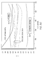
- FIG. 3B shows capacitance versus leakage for the dielectric layers of table 3A.
- the leakage is shown on a logarithmic scale.
- Split 302 demonstrates larger leakage than the other splits.
- the other splits are well grouped and have less than 7 fA/Cell leakage.
- the present invention decreases leakage compared to conventional dielectric layers of comparable thickness.
- FIG. 3C shows capacitance versus BV (breakdown voltage to induce 1 uA) for the dielectric layers of table 3A.
- This figure shows the BV of the 302 split at around 3.0V. This behavior in leakage and BV is indicative of 45 ⁇ nitride. The remaining splits demonstrate higher BV. It is worth noting that the less thick splits, 306 , 307 and 309 even demonstrate a higher BV. A higher BV indicates a large increase in dielectric strength. Thus, it can be seen that the present invention increases dielectric strength.
- FIG. 3D shows the cumulative probability of leakage for the dielectric layers of table 3A.
- the leakage probability of split 302 is unacceptable and all other splits are comparable to split 303 , the 55 ⁇ thick control dielectric layer which is thicker than the other splits.
- FIG. 3E shows the cumulative probability versus capacitance. A 2.5 fF/cell gap is seen between split 303 and the best remaining splits. Thus, it can be seen that the present invention demonstrates an increase in capacitance over conventional dielectrics.
- FIG. 3F shows the cumulative probability versus BV and a significant gap between split 302 and the other splits. This shows that the dielectric layers of the present invention demonstrate improved back voltage characteristics over conventional dielectrics of comparable thickness.
- FIG. 3G shows a performance index C/I (capacitance over current) versus low level voltages for the dielectric layers of table 3A.
- the data for the graph was gathered using keithley CV and IV sweeps.
- the bias voltage was swept from +1V to ⁇ 1V while measuring capacitance.
- the IV sweep swept bias voltage from 0 to ⁇ 1V and measured 20K array current.
- the performance of the 302 split significantly degrades over a range of approximately 0.6V. This performance degradation is a result of leakage increases.
- the best performance of the splits is shown by split 307 which uses 2VP, a processing temperature of 850° C. and a 35 ⁇ thickness.
- FIG. 3H shows the performance index C/I for the various dielectric layers of table 3A.
- the vertical axis is the performance index C/I and the horizontal axis shows the various splits.
- the circles on the right hand side of the graph show the differences between the various dielectric layers. If the circles do not intersect, the difference between splits is significant.
- Splits 307 , 308 and 309 are significantly better in performance than control splits 302 and 303 .
- Table 3A and FIGS. 3B , 3 C, 3 D, 3 E, 3 F, 3 G and 3 H show exemplary experimental results of actual implementations. It can be seen from those figures that thinner dielectric layers fabricated according to the present invention are able to perform as well or better that thicker conventional dielectric layers. Other actual implementations may vary and embodiments of the present invention are not limited to the implementations shown in table 3A and FIGS. 3B , 3 C, 3 D, 3 E, 3 F, 3 G and 3 H.
- FIG. 4 illustrates a transistor semiconductor device utilizing a dielectric layer 402 according to another embodiment of the present invention.
- a source 405 is formed in a substrate 401 .
- a drain 406 is formed in the substrate 401 .
- a gate oxide layer 404 is formed over the substrate 401 from the source 405 to the drain 406 .
- An electrode or gate electrode 403 is formed over the gate oxide layer 404 .
- a dielectric layer 402 is formed over the electrode 403 .
- the dielectric layer 402 is fabricated by vapor depositing a selected material or precursor and subsequently processing those materials.
- the selected material can be deposited by using vapor priming (VP).
- the selected material is a silicon containing material such as silazane or silane type materials.
- An example of a typical silicon-containing material is hexamethyldisilazane (HMDS).
- HMDS hexamethyldisilazane
- Other materials or precursors which may be used are tetramethyldisilazane, octamethylcyclotetrasilazine, hexamethylcyclotrisilazine, diethylaminotrimethylsilane or dimethylaminotrimethylsilane.
- the selected material can be deposited a single time or the depositing can be repeated any number of times.
- the selected material is processed in a reactive ambient to create a final desirable silicon-containing dielectric layer.
- the reactive ambient can be materials such as NH 3 , N 2 , O 2 , O 3 , N 2 , NO and the like and cause silicon atoms of the selected material to react with oxygen atoms, nitrogen atoms or both.
- the resulting silicon-containing dielectric layer is the dielectric layer 402 and can result in a layer that is primarily nitride, primarily oxide or an oxynitride.
- FIG. 5 illustrates use of a silicon-containing dielectric layer 502 in a capacitor according to another embodiment of the present invention.
- the silicon-containing dielectric layer 502 is formed over an electrode 501 .
- the silicon-containing dielectric layer 502 is created by depositing a silicon-containing precursor material from a silazane or silane source. The layer is then processed in a reactive ambient. The reactive ambient causes silicon atoms in the precursor layer to react with oxygen atoms, nitrogen atoms or both to form the silicon-containing dielectric layer.
- a second dielectric layer 503 is formed over the silicon-containing dielectric layer 502 .
- the second dielectric layer 503 may be of a material susceptible to oxygen migration such as Ta 2 O 5 and may be formed using conventional methods.
- the electrode 501 may be composed of a material such as P—Si, SiGe or metal. The remaining capacitor structure is formed according to conventional methodology.
- FIG. 6 is an illustration of a computer system 612 that can use and be used with embodiments of the present invention.
- the computer system 612 would include ROM 614 , mass memory 616 , peripheral devices 618 , and I/O devices 620 in communication with a microprocessor 622 via a data bus 624 or another suitable data communication path.
- the ROM 614 and mass memory 616 can be fabricated using silicon-containing dielectric layers according to the various embodiments of the present invention.
- formation of a material “on” a substrate or layer refers to formation in contact with a surface of the substrate or layer. Formation “over” a substrate or layer refers to formation above or in contact with a surface of the substrate.
- a “substrate” may comprise one or more semiconductor layers or semiconductor structures which may define portions of a semiconductor device.
- Dielectric layers fabricated using the present invention can be used for a variety of purposes. Some examples follow, but embodiments of the present invention are not limited to these.
- a dielectric layer can be used as a covering on a semiconductor device.
- a dielectric layer according to the present invention can be used in a gate structure of a transistor or in an anti-fuse application.
- a dielectric layer according to the present invention can be formed on top of metals to prevent oxidation of metals.
- a dielectric layer according to the present invention can be used in post gate stack and pre oxidation steps to prevent oxygen in-diffusion into active areas of the transistor.
- a dielectric layer according to the present invention can be used to prevent oxidation of gate electrodes with subsequent processing steps when using materials such as polysilicon, Si—Ge, W or other transistion metals.
- a dielectric layer according to the present invention can be used in anti-fuse components of a semiconductor device.
- dielectric layers formed according to the various embodiments of the present invention can be used in a single device and can be stacked or intermixed with other types of dielectric layers.
- Semiconductor devices fabricated utilizing the present invention can be improved compared to other semiconductor devices because the dielectric of this invention can provide an increased dielectric constant and reduced leakage. This may also permit reductions in the size of semiconductor devices.
Abstract
A method of fabricating a semiconductor device including a silicon-containing dielectric layer is provided. In one embodiment, a silicon-containing material is deposited on a substrate. The deposited material is processed with a reactive agent to react with silicon atoms of the deposited material to form the dielectric layer. The silicon-containing dielectric layer provides for improved or smaller semiconductor devices by reducing leakage and increasing the dielectric constant.
Description
This application is a divisional of U.S. patent application Ser. No. 10/273,667 filed Oct. 18, 2002, now U.S. Pat. No. 6,670,231 which is a divisional of U.S. patent application Ser. No. 09/653,096, filed Aug. 31, 2000, now U.S. Pat. No. 6,576,964.
This application is related to commonly assigned U.S. patent application Ser. No. 09/653,639, now U.S. Pat. No. 6,410,968, METHOD FOR FORMING A BARRIER LAYER TO INCREASE SEMICONDUCTOR DEVICE PERFORMANCE, filed Aug. 31, 2000, by Powell et al. and Ser. No. 09/653,298, now U.S. Pat. No. 6,521,544, METHOD FOR FORMING A DIELECTRIC LAYER AT A LOW TEMPERATURE, filed Aug. 31, 2000, by Mercaldi et al., the disclosures of which are incorporated herein by reference.
The present invention relates to the field of semiconductors and, more particularly, to an improved dielectric for increasing semiconductor performance.
There is a constant demand for semiconductor devices of a reduced size. The performance characteristics of semiconductor capacitors, transistors, electrode layers and the like become more critical as device size decreases. Accordingly, processes that result in increased device performance are critical to improved semiconductor device fabrication.
Capacitors generally have two conductive layers or plates separated by an insulator layer or dielectric layer. Capacitor performance can be improved by increasing the dielectric constant of the dielectric material or decreasing the leakage characteristics of the dielectric material.
Accordingly, there is a need in the art for an improved dielectric layer that has improved characteristics such as lower leakage and a higher dielectric constant.
This need is met by the present invention, where a silicon-containing material is deposited over at least a portion of a semiconductor device. The deposited silicon-containing material is processed in a reactive ambient to form the dielectric layer.
In accordance with one embodiment of the present invention, a method for fabricating a semiconductor device is disclosed. According to the method, a substrate having at least one semiconductor layer is provided. A first conductive layer is formed over the substrate. A silicon-containing material is deposited over at least a portion of the semiconductor device. The deposited silicon-containing material is processed in a reactive ambient to form a dielectric layer. A second conductive layer is formed over the dielectric layer.
In accordance with yet another embodiment of the present invention, a semiconductor device is disclosed. The semiconductor device includes a substrate, a first conductive layer, a silicon-containing dielectric layer and a second conductive layer. The first conductive layer is formed over the substrate. The silicon-containing layer is formed over the first conductive layer by reacting silicon atoms from a precursor layer with a reactive agent. The second conductive layer is formed over the silicon-containing layer.
Other methods and devices are disclosed.
The following detailed description of the present invention can be best understood when read in conjunction with the accompanying drawings, where like structure is indicated with like reference numerals.
Generally, conventional dielectric layers are processed using temperature ranges of 700° C. to 1050° C., processing time of 10 seconds to 60 minutes, and processing pressure of 760 torr. Whereas, the dielectric layer of the present invention is typically processed using temperature ranges of 500° C. to 900° C., processing time of 30 seconds to 5 minutes, and processing pressure of 450 torr. However, with silicon sources such as HMDS, the time is not critical because they are self limiting sources. It is contemplated that variations to these ranges may also result in suitable dielectric layer formation.
| TABLE 3A | |||||||
| Split | Wafers | VP | | Dielectric | Thickness | ||
| 301 | 2 | — | 850° | Nitride | 45Å | ||
| 302 | 4, 16 | — | — | | 45Å | ||
| 303 | 6, 18 | — | — | | 55Å | ||
| 306 | 14 | 1 | 850° | Nitride | 35Å | ||
| 307 | 1, 15 | 2 | 850° | Nitride | 35Å | ||
| 308 | 3, 17 | 2 | 850° | Nitride | 45Å | ||
| 309 | 5, 19 | 2 | 950° C. | Nitride | 35Å | ||
Table 3A, shown above, shows experimental results for dielectric layers fabricated utilizing the method of FIG. 2A versus conventional dielectric layers. Here, each split represents a set of dielectric layers fabricated according to the same or similar parameters. Splits 302 and 303 are dielectric layers fabricated according to conventional means with a thickness of 45 Å and 55 Å, respectively. Splits 301 and 306–309 are dielectric layers formed according to the present invention. Split 301 is a dielectric layer fabricated using RTN. Split 306 utilizes a single vapor priming (VP) step and a processing temperature of 850° C. to fabricate a dielectric layer at a thickness of 35 Å. Vapor priming or VP is used to deposit a layer of silicon-containing material. Splits 307–309 perform vapor priming twice to deposit two layers of silicon-containing material. Splits 307 and 308 are processed at a temperature of 850° C. to form dielectric layers of 35 Å and 45 Å, respectively. Split 309 is processes at a temperature of 950° C. to form a dielectric layer having a thickness of 35 Å.
Table 3A and FIGS. 3B , 3C, 3D, 3E, 3F, 3G and 3H show exemplary experimental results of actual implementations. It can be seen from those figures that thinner dielectric layers fabricated according to the present invention are able to perform as well or better that thicker conventional dielectric layers. Other actual implementations may vary and embodiments of the present invention are not limited to the implementations shown in table 3A and FIGS. 3B , 3C, 3D, 3E, 3F, 3G and 3H.
The dielectric layer 402 is fabricated by vapor depositing a selected material or precursor and subsequently processing those materials. The selected material can be deposited by using vapor priming (VP). The selected material is a silicon containing material such as silazane or silane type materials. An example of a typical silicon-containing material is hexamethyldisilazane (HMDS). Other materials or precursors which may be used are tetramethyldisilazane, octamethylcyclotetrasilazine, hexamethylcyclotrisilazine, diethylaminotrimethylsilane or dimethylaminotrimethylsilane. The selected material can be deposited a single time or the depositing can be repeated any number of times. The selected material is processed in a reactive ambient to create a final desirable silicon-containing dielectric layer. The reactive ambient can be materials such as NH3, N2, O2, O3, N2, NO and the like and cause silicon atoms of the selected material to react with oxygen atoms, nitrogen atoms or both. The resulting silicon-containing dielectric layer is the dielectric layer 402 and can result in a layer that is primarily nitride, primarily oxide or an oxynitride.
For the purposes of describing and defining the present invention, formation of a material “on” a substrate or layer refers to formation in contact with a surface of the substrate or layer. Formation “over” a substrate or layer refers to formation above or in contact with a surface of the substrate. A “substrate” may comprise one or more semiconductor layers or semiconductor structures which may define portions of a semiconductor device.
Dielectric layers fabricated using the present invention can be used for a variety of purposes. Some examples follow, but embodiments of the present invention are not limited to these. A dielectric layer can be used as a covering on a semiconductor device. A dielectric layer according to the present invention can be used in a gate structure of a transistor or in an anti-fuse application. A dielectric layer according to the present invention can be formed on top of metals to prevent oxidation of metals. A dielectric layer according to the present invention can be used in post gate stack and pre oxidation steps to prevent oxygen in-diffusion into active areas of the transistor. A dielectric layer according to the present invention can be used to prevent oxidation of gate electrodes with subsequent processing steps when using materials such as polysilicon, Si—Ge, W or other transistion metals. A dielectric layer according to the present invention can be used in anti-fuse components of a semiconductor device.
Additionally, multiple dielectric layers formed according to the various embodiments of the present invention can be used in a single device and can be stacked or intermixed with other types of dielectric layers.
Semiconductor devices fabricated utilizing the present invention can be improved compared to other semiconductor devices because the dielectric of this invention can provide an increased dielectric constant and reduced leakage. This may also permit reductions in the size of semiconductor devices.
Having described the present invention in detail and by reference to preferred embodiments thereof, it will be apparent that modifications and variations are possible without departing from the scope of the present invention defined in the appended claims.
Claims (4)
1. A method of fabricating a semiconductor device comprising:
providing a substrate having at least one semiconductor layer;
forming a conductive layer over the substrate;
vapor priming a first silicon-containing material over the gate oxide;
vapor priming a second silicon-containing material over the first silicon-containing material;
forming a silicon-containing dielectric layer having a thickness of about 35 Å by processing the first silicon-containing material and the second silicon-containing material with a reactive agent selected to react with silicon atoms of the first silicon-containing material and the second silicon-containing material; and
forming a gate electrode over the silicon-containing dielectric layer.
2. The method of claim 1 further comprising:
doping the gate electrode with phosphor.
3. The method of claim 1 further comprising:
doping the gate electrode with boron.
4. The method of claim 1 wherein processing the silicon-containing material in a reactive ambient comprises rapid thermally nitridizing the silicon-containing material in an NH3 ambient at a processing temperature of 850° C.
Priority Applications (1)
| Application Number | Priority Date | Filing Date | Title |
|---|---|---|---|
| US10/706,415 US6998356B2 (en) | 2000-08-31 | 2003-11-12 | Method of fabricating a semiconductor device including a dielectric layer formed using a reactive agent |
Applications Claiming Priority (3)
| Application Number | Priority Date | Filing Date | Title |
|---|---|---|---|
| US09/653,096 US6576964B1 (en) | 2000-08-31 | 2000-08-31 | Dielectric layer for a semiconductor device having less current leakage and increased capacitance |
| US10/273,667 US6670231B2 (en) | 2000-08-31 | 2002-10-18 | Method of forming a dielectric layer in a semiconductor device |
| US10/706,415 US6998356B2 (en) | 2000-08-31 | 2003-11-12 | Method of fabricating a semiconductor device including a dielectric layer formed using a reactive agent |
Related Parent Applications (1)
| Application Number | Title | Priority Date | Filing Date |
|---|---|---|---|
| US10/273,667 Division US6670231B2 (en) | 2000-08-31 | 2002-10-18 | Method of forming a dielectric layer in a semiconductor device |
Publications (2)
| Publication Number | Publication Date |
|---|---|
| US20040106248A1 US20040106248A1 (en) | 2004-06-03 |
| US6998356B2 true US6998356B2 (en) | 2006-02-14 |
Family
ID=24619486
Family Applications (4)
| Application Number | Title | Priority Date | Filing Date |
|---|---|---|---|
| US09/653,096 Expired - Lifetime US6576964B1 (en) | 2000-08-31 | 2000-08-31 | Dielectric layer for a semiconductor device having less current leakage and increased capacitance |
| US10/080,119 Expired - Lifetime US6770574B2 (en) | 2000-08-31 | 2002-02-21 | Method of forming a dielectric layer |
| US10/273,667 Expired - Lifetime US6670231B2 (en) | 2000-08-31 | 2002-10-18 | Method of forming a dielectric layer in a semiconductor device |
| US10/706,415 Expired - Fee Related US6998356B2 (en) | 2000-08-31 | 2003-11-12 | Method of fabricating a semiconductor device including a dielectric layer formed using a reactive agent |
Family Applications Before (3)
| Application Number | Title | Priority Date | Filing Date |
|---|---|---|---|
| US09/653,096 Expired - Lifetime US6576964B1 (en) | 2000-08-31 | 2000-08-31 | Dielectric layer for a semiconductor device having less current leakage and increased capacitance |
| US10/080,119 Expired - Lifetime US6770574B2 (en) | 2000-08-31 | 2002-02-21 | Method of forming a dielectric layer |
| US10/273,667 Expired - Lifetime US6670231B2 (en) | 2000-08-31 | 2002-10-18 | Method of forming a dielectric layer in a semiconductor device |
Country Status (1)
| Country | Link |
|---|---|
| US (4) | US6576964B1 (en) |
Families Citing this family (4)
| Publication number | Priority date | Publication date | Assignee | Title |
|---|---|---|---|---|
| US20030199951A1 (en) * | 2002-04-22 | 2003-10-23 | Pardo Xavier E. | Implantable lead with improved conductor lumens |
| US6734089B1 (en) * | 2003-01-16 | 2004-05-11 | Micron Technology Inc | Techniques for improving wordline fabrication of a memory device |
| US7071117B2 (en) * | 2004-02-27 | 2006-07-04 | Micron Technology, Inc. | Semiconductor devices and methods for depositing a dielectric film |
| US7521378B2 (en) * | 2004-07-01 | 2009-04-21 | Micron Technology, Inc. | Low temperature process for polysilazane oxidation/densification |
Citations (17)
| Publication number | Priority date | Publication date | Assignee | Title |
|---|---|---|---|---|
| US5290736A (en) | 1990-09-25 | 1994-03-01 | Kawasaki Steel Corporation | Method of forming interlayer-insulating film using ozone and organic silanes at a pressure above atmospheric |
| US5304398A (en) | 1993-06-03 | 1994-04-19 | Watkins Johnson Company | Chemical vapor deposition of silicon dioxide using hexamethyldisilazane |
| US5312776A (en) | 1991-11-18 | 1994-05-17 | Matsushita Electric Industrial Co., Ltd. | Method of preventing the corrosion of metallic wirings |
| US5358739A (en) | 1993-02-05 | 1994-10-25 | Dow Corning Corporation | Coating electronic substrates with silica derived from silazane polymers |
| US5525551A (en) | 1993-09-20 | 1996-06-11 | Fujitsu Limited | Method for forming insulating film in semiconductor device using a TEOS or HMDS pre-treatment |
| US5567661A (en) | 1993-08-26 | 1996-10-22 | Fujitsu Limited | Formation of planarized insulating film by plasma-enhanced CVD of organic silicon compound |
| US5814852A (en) | 1995-05-19 | 1998-09-29 | Micron Technology, Inc. | Method of forming a Ta2 O5 dielectric layer, method of forming a capacitor having a Ta2 O5 dielectric layer, and capacitor construction |
| US5844771A (en) | 1996-06-26 | 1998-12-01 | Micron Technology, Inc. | Capacitor construction |
| US5872696A (en) | 1997-04-09 | 1999-02-16 | Fujitsu Limited | Sputtered and anodized capacitors capable of withstanding exposure to high temperatures |
| US5874766A (en) | 1988-12-20 | 1999-02-23 | Matsushita Electric Industrial Co., Ltd. | Semiconductor device having an oxynitride film |
| US5882978A (en) | 1996-10-30 | 1999-03-16 | Micron Technology, Inc. | Methods of forming a silicon nitride film, a capacitor dielectric layer and a capacitor |
| US5917571A (en) | 1996-06-03 | 1999-06-29 | Sharp Kabushiki Kaisha | Active matrix substrate having benzocyclobutene-containing interlayer insulating film and method for fabricating same |
| US6197628B1 (en) | 1998-08-27 | 2001-03-06 | Micron Technology, Inc. | Ruthenium silicide diffusion barrier layers and methods of forming same |
| US6258653B1 (en) | 2000-02-24 | 2001-07-10 | Novellus Systems, Inc. | Silicon nitride barrier for capacitance maximization of tantalum oxide capacitor |
| US6291288B1 (en) | 1999-04-15 | 2001-09-18 | United Microelectronics Corp. | Method of fabricating a thin and structurally-undefective dielectric structure for a storage capacitor in dynamic random-access memory |
| US6444584B1 (en) * | 1998-07-16 | 2002-09-03 | Taiwan Semiconductor Manufacturing Company | Plasma etch method for forming composite silicon/dielectric/silicon stack layer |
| US6686292B1 (en) * | 1998-12-28 | 2004-02-03 | Taiwan Semiconductor Manufacturing Company | Plasma etch method for forming uniform linewidth residue free patterned composite silicon containing dielectric layer/silicon stack layer |
Family Cites Families (2)
| Publication number | Priority date | Publication date | Assignee | Title |
|---|---|---|---|---|
| DE4416720C1 (en) * | 1994-05-11 | 1995-03-23 | Siemens Ag | Method and circuit arrangement for synchronising communication cell streams transmitted redundantly |
| US6245690B1 (en) * | 1998-11-04 | 2001-06-12 | Applied Materials, Inc. | Method of improving moisture resistance of low dielectric constant films |
-
2000
- 2000-08-31 US US09/653,096 patent/US6576964B1/en not_active Expired - Lifetime
-
2002
- 2002-02-21 US US10/080,119 patent/US6770574B2/en not_active Expired - Lifetime
- 2002-10-18 US US10/273,667 patent/US6670231B2/en not_active Expired - Lifetime
-
2003
- 2003-11-12 US US10/706,415 patent/US6998356B2/en not_active Expired - Fee Related
Patent Citations (17)
| Publication number | Priority date | Publication date | Assignee | Title |
|---|---|---|---|---|
| US5874766A (en) | 1988-12-20 | 1999-02-23 | Matsushita Electric Industrial Co., Ltd. | Semiconductor device having an oxynitride film |
| US5290736A (en) | 1990-09-25 | 1994-03-01 | Kawasaki Steel Corporation | Method of forming interlayer-insulating film using ozone and organic silanes at a pressure above atmospheric |
| US5312776A (en) | 1991-11-18 | 1994-05-17 | Matsushita Electric Industrial Co., Ltd. | Method of preventing the corrosion of metallic wirings |
| US5358739A (en) | 1993-02-05 | 1994-10-25 | Dow Corning Corporation | Coating electronic substrates with silica derived from silazane polymers |
| US5304398A (en) | 1993-06-03 | 1994-04-19 | Watkins Johnson Company | Chemical vapor deposition of silicon dioxide using hexamethyldisilazane |
| US5567661A (en) | 1993-08-26 | 1996-10-22 | Fujitsu Limited | Formation of planarized insulating film by plasma-enhanced CVD of organic silicon compound |
| US5525551A (en) | 1993-09-20 | 1996-06-11 | Fujitsu Limited | Method for forming insulating film in semiconductor device using a TEOS or HMDS pre-treatment |
| US5814852A (en) | 1995-05-19 | 1998-09-29 | Micron Technology, Inc. | Method of forming a Ta2 O5 dielectric layer, method of forming a capacitor having a Ta2 O5 dielectric layer, and capacitor construction |
| US5917571A (en) | 1996-06-03 | 1999-06-29 | Sharp Kabushiki Kaisha | Active matrix substrate having benzocyclobutene-containing interlayer insulating film and method for fabricating same |
| US5844771A (en) | 1996-06-26 | 1998-12-01 | Micron Technology, Inc. | Capacitor construction |
| US5882978A (en) | 1996-10-30 | 1999-03-16 | Micron Technology, Inc. | Methods of forming a silicon nitride film, a capacitor dielectric layer and a capacitor |
| US5872696A (en) | 1997-04-09 | 1999-02-16 | Fujitsu Limited | Sputtered and anodized capacitors capable of withstanding exposure to high temperatures |
| US6444584B1 (en) * | 1998-07-16 | 2002-09-03 | Taiwan Semiconductor Manufacturing Company | Plasma etch method for forming composite silicon/dielectric/silicon stack layer |
| US6197628B1 (en) | 1998-08-27 | 2001-03-06 | Micron Technology, Inc. | Ruthenium silicide diffusion barrier layers and methods of forming same |
| US6686292B1 (en) * | 1998-12-28 | 2004-02-03 | Taiwan Semiconductor Manufacturing Company | Plasma etch method for forming uniform linewidth residue free patterned composite silicon containing dielectric layer/silicon stack layer |
| US6291288B1 (en) | 1999-04-15 | 2001-09-18 | United Microelectronics Corp. | Method of fabricating a thin and structurally-undefective dielectric structure for a storage capacitor in dynamic random-access memory |
| US6258653B1 (en) | 2000-02-24 | 2001-07-10 | Novellus Systems, Inc. | Silicon nitride barrier for capacitance maximization of tantalum oxide capacitor |
Also Published As
| Publication number | Publication date |
|---|---|
| US20020135031A1 (en) | 2002-09-26 |
| US20040106248A1 (en) | 2004-06-03 |
| US6576964B1 (en) | 2003-06-10 |
| US6670231B2 (en) | 2003-12-30 |
| US20030052338A1 (en) | 2003-03-20 |
| US6770574B2 (en) | 2004-08-03 |
Similar Documents
| Publication | Publication Date | Title |
|---|---|---|
| US5780115A (en) | Methods for fabricating electrode structures including oxygen and nitrogen plasma treatments | |
| US6943078B1 (en) | Method and structure for reducing leakage current in capacitors | |
| US5861651A (en) | Field effect devices and capacitors with improved thin film dielectrics and method for making same | |
| US6306742B1 (en) | Method for forming a high dielectric constant insulator in the fabrication of an integrated circuit | |
| US7245010B2 (en) | System and device including a barrier layer | |
| US6734068B2 (en) | Method to form silicates as high dielectric constant materials | |
| US6989565B1 (en) | Memory device having an electron trapping layer in a high-K dielectric gate stack | |
| US20060275991A1 (en) | Method of manufacturing a semiconductor integrated circuit device | |
| US5554558A (en) | Method of making high precision w-polycide-to-poly capacitors in digital/analog process | |
| US6831319B2 (en) | Cell nitride nucleation on insulative layers and reduced corner leakage of container capacitors | |
| JPH06151751A (en) | Semiconductor integrated circuit device and manufacture thereof | |
| US6998356B2 (en) | Method of fabricating a semiconductor device including a dielectric layer formed using a reactive agent | |
| JPH0621333A (en) | Method for fabricating semiconductor device | |
| US6635524B2 (en) | Method for fabricating capacitor of semiconductor memory device | |
| JP3219856B2 (en) | Method for manufacturing semiconductor device | |
| JP3316210B2 (en) | Method for manufacturing semiconductor device | |
| KR19980065739A (en) | Capacitor Manufacturing Method of Semiconductor Memory Device | |
| JPH0945901A (en) | Mis semiconductor device | |
| JPH0750395A (en) | Semiconductor memory device and manufacture thereof | |
| JPH04275454A (en) | Manufacture of semiconductor device |
Legal Events
| Date | Code | Title | Description |
|---|---|---|---|
| FEPP | Fee payment procedure |
Free format text: PAYOR NUMBER ASSIGNED (ORIGINAL EVENT CODE: ASPN); ENTITY STATUS OF PATENT OWNER: LARGE ENTITY |
|
| FPAY | Fee payment |
Year of fee payment: 4 |
|
| REMI | Maintenance fee reminder mailed | ||
| LAPS | Lapse for failure to pay maintenance fees | ||
| STCH | Information on status: patent discontinuation |
Free format text: PATENT EXPIRED DUE TO NONPAYMENT OF MAINTENANCE FEES UNDER 37 CFR 1.362 |
|
| FP | Lapsed due to failure to pay maintenance fee |
Effective date: 20140214 |