US6992676B2 - Image display system - Google Patents
Image display system Download PDFInfo
- Publication number
- US6992676B2 US6992676B2 US10/916,454 US91645404A US6992676B2 US 6992676 B2 US6992676 B2 US 6992676B2 US 91645404 A US91645404 A US 91645404A US 6992676 B2 US6992676 B2 US 6992676B2
- Authority
- US
- United States
- Prior art keywords
- data
- image
- display device
- pixels
- compressed data
- Prior art date
- Legal status (The legal status is an assumption and is not a legal conclusion. Google has not performed a legal analysis and makes no representation as to the accuracy of the status listed.)
- Expired - Lifetime
Links
Images


Classifications
-
- H—ELECTRICITY
- H04—ELECTRIC COMMUNICATION TECHNIQUE
- H04N—PICTORIAL COMMUNICATION, e.g. TELEVISION
- H04N5/00—Details of television systems
- H04N5/44—Receiver circuitry for the reception of television signals according to analogue transmission standards
-
- G—PHYSICS
- G06—COMPUTING; CALCULATING OR COUNTING
- G06F—ELECTRIC DIGITAL DATA PROCESSING
- G06F3/00—Input arrangements for transferring data to be processed into a form capable of being handled by the computer; Output arrangements for transferring data from processing unit to output unit, e.g. interface arrangements
- G06F3/14—Digital output to display device ; Cooperation and interconnection of the display device with other functional units
-
- G—PHYSICS
- G09—EDUCATION; CRYPTOGRAPHY; DISPLAY; ADVERTISING; SEALS
- G09G—ARRANGEMENTS OR CIRCUITS FOR CONTROL OF INDICATING DEVICES USING STATIC MEANS TO PRESENT VARIABLE INFORMATION
- G09G3/00—Control arrangements or circuits, of interest only in connection with visual indicators other than cathode-ray tubes
- G09G3/20—Control arrangements or circuits, of interest only in connection with visual indicators other than cathode-ray tubes for presentation of an assembly of a number of characters, e.g. a page, by composing the assembly by combination of individual elements arranged in a matrix no fixed position being assigned to or needed to be assigned to the individual characters or partial characters
- G09G3/34—Control arrangements or circuits, of interest only in connection with visual indicators other than cathode-ray tubes for presentation of an assembly of a number of characters, e.g. a page, by composing the assembly by combination of individual elements arranged in a matrix no fixed position being assigned to or needed to be assigned to the individual characters or partial characters by control of light from an independent source
- G09G3/36—Control arrangements or circuits, of interest only in connection with visual indicators other than cathode-ray tubes for presentation of an assembly of a number of characters, e.g. a page, by composing the assembly by combination of individual elements arranged in a matrix no fixed position being assigned to or needed to be assigned to the individual characters or partial characters by control of light from an independent source using liquid crystals
- G09G3/3611—Control of matrices with row and column drivers
- G09G3/3648—Control of matrices with row and column drivers using an active matrix
- G09G3/3659—Control of matrices with row and column drivers using an active matrix the addressing of the pixel involving the control of two or more scan electrodes or two or more data electrodes, e.g. pixel voltage dependant on signal of two data electrodes
-
- G—PHYSICS
- G09—EDUCATION; CRYPTOGRAPHY; DISPLAY; ADVERTISING; SEALS
- G09G—ARRANGEMENTS OR CIRCUITS FOR CONTROL OF INDICATING DEVICES USING STATIC MEANS TO PRESENT VARIABLE INFORMATION
- G09G2300/00—Aspects of the constitution of display devices
- G09G2300/08—Active matrix structure, i.e. with use of active elements, inclusive of non-linear two terminal elements, in the pixels together with light emitting or modulating elements
- G09G2300/0809—Several active elements per pixel in active matrix panels
- G09G2300/0814—Several active elements per pixel in active matrix panels used for selection purposes, e.g. logical AND for partial update
-
- G—PHYSICS
- G09—EDUCATION; CRYPTOGRAPHY; DISPLAY; ADVERTISING; SEALS
- G09G—ARRANGEMENTS OR CIRCUITS FOR CONTROL OF INDICATING DEVICES USING STATIC MEANS TO PRESENT VARIABLE INFORMATION
- G09G2320/00—Control of display operating conditions
- G09G2320/02—Improving the quality of display appearance
- G09G2320/0266—Reduction of sub-frame artefacts
-
- G—PHYSICS
- G09—EDUCATION; CRYPTOGRAPHY; DISPLAY; ADVERTISING; SEALS
- G09G—ARRANGEMENTS OR CIRCUITS FOR CONTROL OF INDICATING DEVICES USING STATIC MEANS TO PRESENT VARIABLE INFORMATION
- G09G2340/00—Aspects of display data processing
- G09G2340/02—Handling of images in compressed format, e.g. JPEG, MPEG
-
- G—PHYSICS
- G09—EDUCATION; CRYPTOGRAPHY; DISPLAY; ADVERTISING; SEALS
- G09G—ARRANGEMENTS OR CIRCUITS FOR CONTROL OF INDICATING DEVICES USING STATIC MEANS TO PRESENT VARIABLE INFORMATION
- G09G2340/00—Aspects of display data processing
- G09G2340/04—Changes in size, position or resolution of an image
- G09G2340/0407—Resolution change, inclusive of the use of different resolutions for different screen areas
-
- G—PHYSICS
- G09—EDUCATION; CRYPTOGRAPHY; DISPLAY; ADVERTISING; SEALS
- G09G—ARRANGEMENTS OR CIRCUITS FOR CONTROL OF INDICATING DEVICES USING STATIC MEANS TO PRESENT VARIABLE INFORMATION
- G09G3/00—Control arrangements or circuits, of interest only in connection with visual indicators other than cathode-ray tubes
- G09G3/20—Control arrangements or circuits, of interest only in connection with visual indicators other than cathode-ray tubes for presentation of an assembly of a number of characters, e.g. a page, by composing the assembly by combination of individual elements arranged in a matrix no fixed position being assigned to or needed to be assigned to the individual characters or partial characters
- G09G3/2007—Display of intermediate tones
- G09G3/2018—Display of intermediate tones by time modulation using two or more time intervals
- G09G3/2022—Display of intermediate tones by time modulation using two or more time intervals using sub-frames
- G09G3/2025—Display of intermediate tones by time modulation using two or more time intervals using sub-frames the sub-frames having all the same time duration
Definitions
- the present invention relates to an image display system, and more particularly to an image display system suitable for performing a signal processing of a color image data using a compressed data.
- a CRT Cathode Ray Tube
- a display for each pixel by projecting an electron beam that is narrowly focused, onto a surface of a fluorescent material, and then to display a color image over an entire screen by scanning the electron beam.
- the number of pixels that constitute the screen has been increased comparing to the conventional television broadcasting.
- a display device that is used in a computer terminal and the like, at a time when enhancing a quality of an image, it is adopted a system of increasing the number of rewritings (frame rates) of the display screen as well as an increase of the number of pixels.
- a liquid crystal display device a plasma display device and the like
- a structure (configuration) of constituting a pixel that becomes a unit of a display as a circuit-like, and of displaying a color image on a screen by supplying a display signal to each pixel while selecting each pixel.
- this kind of display device it is constituted to display a color image by inputting data with respect to a color image through a wire from a display control device that creates or stores a display data, supplying the inputted data to each pixel using a driver circuit, and then driving each pixel sequentially.
- a method of enhancing a quality of an image to be displayed increasing the number of pixels within the screen and/or of increasing the frame rate are/is adopted.
- enhancing an image quality is equivalent to increasing an amount of information to be sensed visually, and this is eventually equivalent to increasing an amount of data to be displayed.
- an enhancement of an image quality can be planned, by simply increasing the number of pixels that constitute the screen, or increasing the number of rewritings (the frame rate “f”) of the display screen, as in the conventional technology.
- the frame rate “f” the number of rewritings
- a processing time for a sheet of screen is “pf”
- a time required for a generation or an input of a display data is “pi”
- a transfer time of the display data is “pt”
- the processing time “pf” for the sheet of screen is proportional to the number of pixels, then increasing the number of pixels for the purpose of an enhancement of the image quality causes the processing time “pf” to be extended, and eventually this causes the frame rate “f” to be decreased.
- a so-called VGA screen is constituted of 640 horizontal pixels and 480 vertical pixels
- a so-called UXGA screen is constituted of 3200 horizontal pixels and 2400 vertical pixels
- the ratio of the number of pixels between two screens is 1:25.
- a screen of 30 frames per second is transmitted for reproducing and displaying the motion pictures, and on one hand, for a screen display of a computer terminal and the like, a high frame rate such as 120 frame per second is set up, for example, and the ratio between the frame rates in both cases is 1:4.
- an amount of data for a display is a multiplication of the frame rate and the number of pixels, and the ratio of the amount of data in both cases is 1:100.
- the increased data can be easily transferred, if the frame rate is made to be higher, but if the transfer condition of the data transfer path is 30 frames/second, then for transferring the data corresponding to 120 frames/second, the amount of data transfer is restricted by the transfer condition, and thus it can not be dealt with the increase of the amount of data.
- a processing time largely depends on a capability of a device that performs a screen display, and thus it is possible that the device for generating the data and the device for receiving the data have the different capabilities. For example, if a generation capability of a display data is equivalent to the one of television broadcasting, when the display device has the ability of the QUXGA, then an image that can be displayed in practice is equivalent to the one of the television broadcasting. Conversely, even if the processing time “pf” is shortened by increasing the capability of the device that performs the processing, there is a case that an upper limit value of the frame rate “f” possessed by the display device becomes a restriction. As described above, at a time when processing the image data, if the capabilities of the device for generating the data and of the device for receiving the data are not managed, the capabilities of devices can not be utilized sufficiently as a whole system.
- a control device which includes a compressed data generation unit for generating a compressed data based on a set-up value inputted, and a controller for outputting a frame rate information to the compressed data generation unit, and for making compressed data to be outputted from a memory for use in storing a compressed data to an image display device in accordance with the frame rate.
- an image display system which includes an image display device for displaying an image in accordance with an image information, a memory for storing a compressed data, and a controller for making the compressed data to be outputted from the memory to the image display device in accordance with a frame rate.
- an image display system which includes an image display device for displaying an image in accordance with an image information, a compressed data generation unit for generating a compressed data based on a frame rate and an image information, and a controller for outputting an information of a frame rate to the compressed data generation unit.
- an image display system which includes an image display device for displaying an image in accordance with an image information, a compressed data generation unit for generating a compressed data based on a frame rate and an image information, and a controller for outputting a frame rate information to the compressed data generation unit, and for making the compressed data to be outputted from a memory for use in storing a compressed data to the image display device in accordance with the frame rate.
- an information processing device which includes an image display device for displaying an image in accordance with an image information, and a control device for outputting an image information to the image display device, wherein the control device includes an image information generation unit for generating an image information, a compressed data generation unit for generating a compressed data based on a frame rate and an image information, and a controller for outputting a frame rate information to the compressed data generation unit, and for making the compressed data to be outputted from a memory for use in storing a compressed data to the image display device in accordance with the frame rate.
- a television receiver which includes an image display device for displaying an image in accordance with an image information, and a control device for outputting an image information to the image display device
- the control device includes a receiving unit for receiving an image information, a compressed data generation unit for generating a compressed data based on a frame rate and an image information received by the receiving unit, and a controller for outputting a frame rate information to the compressed data generation unit, and for making the compressed data to be outputted from a memory for use in storing a compressed data to the image display device in accordance with the frame rate.
- a transmitter which includes an image information generation unit for generating an image information, a compressed data generation unit for generating a compressed data in accordance with a predetermined transmission rate and the image information, and a transmission unit for transmitting the compressed data.
- an image distribution system which includes a first recording unit for recording a distribution request from a user and an information about an image display device of which the user possesses, on a recording medium through a telecommunication line, a second recording unit for recording a transmission rate of an image information on the recording medium, a compressing unit for compressing an image information to be displayed on the image display device, in accordance with the distribution request, the information about the image display device and the transmission rate, a transmission unit for transmitting the compressed image information, and an accounting unit for processing the distribution request recorded on the recording medium or the information of the image display device, and for performing an accounting in response to a result of the processing.
- the above-described units it is configured to change the compression rate of data along with the frame rate, so that the increase in the load of the data transfer can be suppressed for the increase of the amount of data. More concretely, by increasing the data compression rate along with the increase of the frame rate, the contrary conditions of the number of pixels and of the frame rate can be relaxed. As a result, by transferring the compressed data in which the compression rate of data has been changed along with the frame rate to the image display device, it can be contributed to an enhancement of the image quality.
- FIG. 1A is a block diagram showing a structure of an image display system according to one embodiment of the present invention.
- FIG. 1B is a block diagram showing a structure of an image display system according to another embodiment of the present invention.
- FIG. 2 is a block diagram showing a structure of a display device according to the present invention.
- FIG. 3 is a diagram for illustrating the structures of an address generation control signal and a compressed data generation control signal
- FIG. 4 is a diagram for illustrating a relationship between a diagram structure and a pixel block
- FIG. 5 is a diagram for illustrating a relationship between a display device and a display data in a compression rate set-up
- FIG. 6 is a diagram for illustrating a transfer method of a compressed data
- FIG. 7 is a diagram for illustrating a generation method of a compressed data
- FIG. 8 is a block diagram showing an entire structure of a display device according to the present invention.
- FIG. 9 is diagram enlargedly showing a portion of a display area in order to illustrate a write situation into a pixel for each frame in the embodiment shown in FIG. 8 ;
- FIG. 10 is a circuit diagram showing an embodiment of a pixel circuit structure for implementing an image area separation display according to the present invention.
- FIG. 11 is a timing chart showing an example of a driving voltage waveform to be applied to each wire, in order to perform the image area separation display according to the present invention
- FIG. 12 is a block diagram showing an entire structure of a display device according to another embodiment of the present invention.
- FIG. 13 is a circuit diagram showing an example of the pixel unit 300 shown in FIG. 12 ;
- FIG. 14 is a circuit diagram showing an example of a detailed circuit structure of the pixel unit 300 shown in FIG. 12 ;
- FIG. 15 is a diagram for illustrating an operation of the signal comparator shown in FIG. 14 ;
- FIG. 16 is a diagram for illustrating a control operation of the display device shown in FIG. 12 ;
- FIG. 17 is a timing chart for illustrating a control operation of the display device shown in FIG. 12 ;
- FIG. 18 is a diagram for illustrating a negotiation procedure of a device capability
- FIG. 19 is a diagram for illustrating a negotiation of a device capability
- FIG. 20 is a diagram for illustrating a data structure of a data transfer
- FIG. 21 is a block diagram showing a structure at a time when applying the present invention to a transmitter
- FIG. 22 is a block diagram showing a structure at a time when applying the present invention to an image distribution system
- FIG. 1A is a block diagram showing a structure of an image display system according one embodiment of the present invention.
- the image display system is constituted of a display control device 200 , a data transfer device 211 , and a display device (image display device) 212 .
- the display control device 200 is configured to, as an element of a video card, input a screen structure of the display device 212 , a data concerning a frame rate (frame rate information) or a color image data as an image information, from a keyboard, for example, to compress the inputted data in a compression rate (data compression rate) matching with a frame rate, and to transfer the compressed data to the display device 212 through the data transfer device 211 .
- a compression rate data compression rate
- FIG. 1B it may also adopt a structure to input an image information, for example, a color image data, according to a generation of the processor (CPU) 210 connected to the display control device 200 , and then to compress the inputted data in the display control device 200 .
- the display device 200 is, as shown in FIG. 2 , constituted of a management unit 201 , a compressed data generation unit 202 , a compressed data memory 203 , and an address generation unit 204 .
- the management unit 201 is configured to input a data including a screen structure, a frame rate, and a color image information, to generate a compressed data generation control signal and an address generation control signal based on the inputted data, to output the compressed data generation control signal to the compressed data generation unit 202 , and to output the address generation control signal to the address generation unit 204 .
- the compressed data generation signal and the address generation signal are, as shown in FIG. 3 , constituted of signals including information of a frame rate (100 fps, 50 fps, . . . ), a block size (1000 ⁇ 1000, 640 ⁇ 480, . . . ), a number of analogous colors (two colors, four colors, . . . ), areas (animation area, still-picture area, . . . ), and a clock.
- the address generation unit 204 is configured to generate a write address and a read address, as a memory address associated with each pixel that constitutes the color image, in response to the address generation control signal, and to sequentially output the memory addresses for the write/read to the compressed data memory 203 .
- the memory address for writing the data is generated using the information such as a format and a timing of the data input, a type of the compressed data, a screen structure of the display device 212 and the like.
- the memory address for reading the data is generated using the information such as a type of the compressed data, a screen structure of the display device 212 , a frame rate and the like.
- the compressed address generation unit 202 is configured to compress the color image data, in accordance with the frame rate as the set-up value (predetermined value), in response to the compressed data generation control signal, and to transfer the compressed data together with a header information to the compressed data memory 203 .
- the compressed data memory 203 is configured to store the compressed data into a designated memory area in response to the memory address for the write, as a memory (storage medium) for storing the compressed data, to read the compressed data from the designated memory area in response to the memory address for the read, and to output the compressed data read as a display data to the data transfer device 211 .
- the management unit 201 , the address generation unit 204 are configured to have an capability of a controller so as to output an information concerning the frame rate to the compressed data generation unit 202 , at a time when the data concerning the color image data is inputted, as well as to read the compressed data from the compressed data memory 203 , in response to the frame rate, and then to cause the compressed data read, as a display data, to be outputted to the display device 212 through the data transfer device 211 .
- the compressed data generated by the compressed data generation unit 202 is generated in that a block of which a plurality of pixels are combined is a unit, as shown in FIG. 4 . It is performed with the block unit when the compressed data generated by the compressed data generation unit 202 is transferred or stored, as well as it is performed with the block unit when an elongation-process is performed on the transferred data.
- the parameters such as a shape and a size of this block, a number of pixels to be included in the block may be set-up with a fixed value, or it may be set-up as variables based on the characteristics of the image signal, and a compression rate may be established based on the set-up parameters.
- the parameters may be set-up as variables by separating the image areas based on the signal characteristics.
- a compressed data it may be generated by implementing a compression process as making an image data for a pixel (of a pixel unit) inputted from the processor 210 to be a subject thereto, or a compressed data may be generated based on a plotting command.
- the data transfer device 211 may be constituted of a data transmission line in which a lead is used, as well as of a wireless data transmitting means or an optical data transmission line.
- the image data by the compressed data is transferred along with a control signal, and an electric power may be transmitted simultaneously if necessary.
- the image data to be transferred follows with a predefined data format, a transmission procedure and the like, the same image data may be rearranged on the receiving side, i.e., the display device 212 side.
- the data transfer device 211 is in that an upper limit of a rate with which a data transfer can be made stably is defined in many cases, and in general, a transfer rate is expressed in a unit of bps (bit per second) and the like. This value is to define a time “pt” required for a certain data transfer. Under the condition as the time “pt” being defined, in the present embodiment, as will be described later, assuming the data to be transferred as a compressed type, it is arranged that a substantial transfer rate is enhanced, and the process time “pt” is shortened.
- the display device 212 is constituted by using a liquid crystal display device of an active matrix type, for example, and an upper limit “fup” of a physical frame rate possessed by the display device itself is set-up, by electrical operation conditions such as an element structure, a wiring, a driver structure and the like.
- an operation condition can be eased by reducing an amount of signal to be driven by a driver, thereby it is arranged to enhance the frame rate “fup” of the display device 212 itself.
- a compatibility of an interface can be implemented, because an operation of a driver of the display device 212 , a signal flowing through a wiring, and the like become the same as the ones of the conventional driving conditions per pixel unit.
- the processing time “pf” could be 1/2 as a result of the compression rate of data being 1/2, then, from the above-mentioned relational expression, the frame rate capable of displaying the inputted data can be set-up in two-holds.
- the upper limit value “fup” defined by the device capability of the display device itself can not be exceeded. Accordingly, the processing time “pf” can be defined as the upper limit value “fup” being the constraint.
- the display control device 200 performing a negotiation procedure for exchanging the capabilities among the devices, a set-up of the compressed data type, the image area separation based on the image content, and adjusting the processing time “pf” and the display frame “f”, it is also possible to enhance the image quality while utilizing the device capabilities.
- an influential factor of the processing time “pf” becomes the data transfer time “pt”.
- the processing time can not be established in advance, and thus the device design becomes difficult.
- the processing time can be established in advance by adopting a compression system in which the compression rate is to be fixed by the parameter set-up, as in the present invention.
- the commands concerning the screen 1 to the screen 4 are inputted based on the start directive and the terminate directive of the operator, the compressed data 1 to 4 concerning the screen 1 to 4 are generated based on the commands inputted, and it makes possible to display the images that follow the respective commands onto the screen of the display device 212 by iterating the processes of transferring the compressed data 1 to 4 to the display device 212 through the data transfer device 211 after having stored the compressed data 1 to 4 into the compressed data memory 203 .
- the frame rate of the display is substantially controlled by the data transfer time, in order to shorten the transfer time, utilizing the compressed data may enhance the frame rate.
- the generation time “pi” of the compressed data as seeing from the data output side could-be made approximately zero “0” by constituting the compressed data memory 203 with the one having the capacity to store the compressed data for two screens, for example, two memories, as well as constituting the switches on both sides of each memory, and arranging them (the switches) to enable the processes of writing the data for one screen into one of the memories through one of the switches, and reading the data for one screen from the other memory through the other switch, and thereby alternately switching the memories which perform the reading of data and the writing of data.
- the processes of writing the data and of reading the data in the block unit could be performed simultaneously by arranging the memory in a dihedral structure.
- the compressed data memory 203 may be no longer required by arranging the generation of the compressed data to be faster than the data transfer rate.
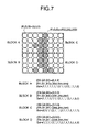
- the inputted image is a two-dimensional image of which several pixels are arranged on a plane, the inputted image is divided into a block constituted of a plurality of pixels, and the compression processing procedures for a block unit is performed.
- a size of the block is not restricted, but it may be configured as 4 (four) in vertical and 4 (four) in horizontal (total 16 pixels/block), as shown in FIG. 7 , for example.
- the color signal C may be any one of the RGB. Further, it may be varied for each block.
- a pixel of the white background is set-up to 1
- a pixel constituting the character is set-up to 0, respectively.
- the inside of block is represented by the two kinds (white and black) of analogous color signals, but it is not intended to limit the kind and the number thereof. Further, as he parameters of the compression processes, the block size, the kind of analogous colors within the block, the number of bits for the color signal and the like may be set-up.
- each pixel is classified according to only a single color signal C.
- the grouping may be made by performing a distance calculation on a color space.
- the parameters such as the block size, the number of analogous colors within the block and the like may be modified arbitrarily in the above-mentioned procedures.
- the compression rate may be set-up along with this set-up of the parameters.
- FIG. 8 is a block diagram showing an entire structure of the image display device 212 .
- the image display device 212 in the present embodiment is constituted of a display controller 10 , an image conversion circuit 11 , and a display panel 15 .
- the display controller 10 converts the image data (compressed data) from the data transfer device 211 to a display data.
- the image conversion circuit 11 is constituted of a frame memory, which sends the data with different resolutions to the display panel 15 , and an animation discriminate circuit.
- a signal driver 12 for applying an image data signal to the display panel 15 On the periphery of the display panel 15 , a signal driver 12 for applying an image data signal to the display panel 15 , a gate driver 13 for applying a scanning signal to the display panel 15 , and a pixel selection driver 14 for applying a selection signal which selects a display block are arranged.
- the display panel 15 is capable of optionally switching an animation area 15 A in which a plurality of pixels within one block is selected in one scanning period of time simultaneously and the same content is displayed, and a still-picture area 15 B in which a plurality of pixels within 1 block are selected by multiple times of scanning and the different displays are possible for each selection, with a plurality of pixels among which several pixels are arranged in a matrix shape as 1 block unit.
- the image display device 212 of the present embodiment for the plurality of pixels, it implements a smooth display of an animation by displaying the data with the low resolution in one scanning period of time simultaneously, and it also implements a highly minute display of a still-picture by displaying the data with high resolution in multiple times.
- the animation area 15 A in which input signals from the signal driver 12 , the gate driver 13 and the pixel selection driver 14 are selected for a plurality of pixels within one block in one scanning period of time simultaneously and the same content is displayed
- the still-picture area 15 B in which the input signals are selected by the scanning of multiple times, for the plurality of pixels within 1 block and the different displays are possible for each selection may be optionally selected, and the sizes and the display locations may be changed.
- one pixel is constituted of 3 pixels of red, green and blue, and for a case of the monochrome display, it is assumed that one pixel is equal to one pixel.
- FIG. 9 is a diagram enlargedly showing a portion of the display area for illustrating a write situation into a pixel for each frame in the present embodiment.
- 4 pixels of 2 ⁇ 2 pixels are defined as 1 block unit.
- the high minute still-picture area writes the image data a (1) 1,1 into the pixel 150 , and similarly, to other high minute still-picture areas, the image data is written into one pixel within four pixels, respectively.
- the low minute animation area writes the same image data a (1) 3,0 into four pixels 160 , and similarly, to other low minute animation areas, the same image data is written into four pixels, respectively.
- the high minute still-picture area holds the image data a (1) 1,1 of the pixel 150 written into the previous frame, and newly writes the image data a( 2 ) 1,2 into the pixel 151 which is different from the previous frame within the block, and similarly, to other high minute still-picture areas, the image data is written into one pixel that is different from the previous frame, respectively.
- the low minute animation area writes the same and the new image data a (2) 3,0 into four pixels 161 , and similarly, to other low minute animation areas, the same and new image data is written into four pixels, respectively.
- the high minute still-picture area holds the image data of the pixels 150 , 151 written into the first and second frames, and newly writes the image data a (3) 1,3 into the pixel 152 which is different from the first and second frames within the block, and similarly, to other high minute still-picture areas, the image data is written into one pixel that is different from the first and second frames, respectively.
- the low minute animation area writes the same and the new image data a (3) 3,0 into four pixels 162 , and similarly, to other low minute animation areas, the same and new image data is-written into four pixels, respectively.
- the high minute still-picture area holds the image data of the pixels 150 , 151 , 152 written into the first, second and third frames, and newly writes the image data a (4) 1,4 into the pixel 153 which is different from the first, second and third frames within the block, and similarly, to other high minute still-picture areas, the image data is written into one pixel that is different from the first, second and third frames, respectively.
- the low minute animation area writes the same and the new image data a (4) 3,0 into four pixels 163 , and similarly, to other low minute animation areas, the same and new image data is written into four pixels, respectively.
- the high minute still-picture display area and the low minute animation display area can be displayed in arbitrary areas within the display area.
- the high minute still-picture area forms a high minute image with four frames, and the low minute animation area can display a new data for each frame. Accordingly, the still-picture having no variation within four frames can be displayed in a high minute, and the animation with a rapid motion can be fast-displayed for each frame.
- a display system for displaying by varying a resolution of an arbitrary area within a display area as described above is called as an image area separation display system.
- FIG. 10 is a circuit diagram showing an embodiment of a pixel circuit structure for implementing an image area separation display according to the present invention.
- the present embodiment is a pixel circuit structure of which 2 ⁇ 2 pixels are made as 1 block unit, and an entire display area of the display panel 15 is formed by arranging a large number of this pixel circuit structures.
- One block unit is not restricted to four pixels. However, in considering a degradation of an opening ratio caused by an increase of wiring and the like, one block with four pixels is preferable.
- the image display device using the image area separation display system of the present invention is not restricted to the liquid crystal display, and it is applicable to the ELD, FED, PDP and the like.
- the present invention will be described with the liquid crystal display that is the most suitable as an example.
- the liquid crystal display of the present embodiment is constituted of an illumination device on the background, and includes a pair of transparent substrates having polarizing plates and a liquid crystal layer sandwiched between these pair of transparent substrates, and is configured to control an orientation state of the liquid crystal layer by applying an electrical field to the liquid crystal layer, and to display an image.
- one block is formed by four pixels of the pixels 50 A, 50 B, 50 C, 50 D.
- the pixel 50 A is constituted of three pixels of the Red 50 AR, the Green 50 AG, and the Blue 50 AB.
- the pixel 50 B is constituted of three pixels of the Red 50 BR, the Green 50 BG, and the Blue 50 BB.
- the pixel 50 C is constituted of three pixels of the Red 50 CR, the Green 50 CG, and the Blue 50 CB.
- the pixel 50 D is constituted of three pixels of the Red 50 DR, the Green 50 DG, and the Blue 50 DB.
- a scanning wiring 20 that is a common to the four pixels is formed at a center, and twelve gates of the thin film transistors 24 AR, 24 BR, 24 CB, 24 DB and the like that are the first switches are connected to the scanning wiring 20 .
- a block selection signal wiring 21 A is connected to the drain electrodes of the thin film transistors 24 AR, 24 AG, and 24 AB that are the first switches.
- a block selection signal wiring 21 B is connected to the drain electrodes of the thin film transistors 24 BR, 24 BG, and 24 BB.
- a block selection signal wiring 21 C is connected to the drain electrodes of the thin film transistors 24 CR, 24 CG, and 24 CB.
- a block selection signal wiring 21 D is connected to the drain electrodes of the thin film transistors 24 DR, 24 DG, and 24 DB.
- the thin film transistors 24 AR, 24 AG, 24 AB that are the first switches are the switches for selecting the pixel 50 A, respectively, and can also be formed as one by a commonization. Similarly to the pixels 50 B, 50 C, 50 D, the first switches can also be formed as one by a commonization.
- Twelve gate electrodes of the thin film transistors 23 AR, 23 BR, 23 CB, 23 CB and the like that are the second switches are connected to the source electrodes of the thin film transistors that are the first switches.
- a red color image signal wiring 22 R, a green color image signal wiring 22 G, and a blue color image signal wiring 22 B are connected to the drain electrodes of the thin film transistors that are the second switches, respectively.
- the pixel electrodes are connected, respectively, and the counter electrodes 26 AR, 26 BR, 26 CB, 26 DB and the like are connected thereto, by sandwiching the liquid crystal layer, so that they form the pixel units 25 AR, 25 BR, 25 CB, 25 DB and the like.
- the counter electrodes are the electrodes that are common to all pixels.
- the holding capacitors are formed in parallel.
- the scanning wiring 20 is connected to the gates of the first switches and the block selection signal wiring is connected to the drain electrodes of the first switches, but it may be arranged as a structure of which the block signal selection wiring for each pixel is connected to the respective gates, and the scanning wiring 20 is connected to the drain electrodes of all four pixels.
- FIG. 11 is a timing-chart showing an example of a driving voltage waveform to be applied to each wiring in FIG. 10 in order to perform an image area separation display.
- a gate voltage 30 which turns on the thin film transistors that are first switches for every frame period of time 34 is applied.
- the voltages 32 A to 32 D are applied to the block selection signal wiring X(i) 1 to X(i) 4 21 A to 21 D for each 4 blocks, respectively, and in synchronization with the gate voltage 30 , the image signals 31 corresponding to the red color D(i)R, the green color D(i)G, and the blue color D(i)B are applied to the pixels through the second switches.
- the voltages are held, during four (4) frames.
- the voltage 33 is applied to 21 A to 21 D that are the block selection signal wiring X(i) all for each frame, respectively, and in synchronization with the gate voltage 30 , the image signals 31 corresponding to the red color D(i)R, the green color D(i)G, and the blue color D(i)B are applied to the pixels through the second switches. Accordingly, the same signal is applied to all of the pixels 50 A, 50 B, 50 C, 50 D, and thus the same display for four pixels can be rewritten for each frame.
- the j+1-th scanning wiring Y(j+1) similarly to the j-th wiring, it discriminates whether it is the high minute display area or the low minute display area, and by inputting the above-mentioned driving waveform, it makes possible a display of an image area separation.
- FIG. 12 is a block diagram showing an entire structure of the display device 212 according to the present invention.
- the display device 212 in the present embodiment is constituted of n-levels of gray approximation arithmetic circuit 310 for converting the inputted image signal to a n-levels of gray approximate image signal approximated to a gray level of a binary value for each block, a signal control circuit 320 for supplying predetermined signals to the X driver 330 , the Y driver 340 , the common voltage generation circuit 350 , and the signal supply circuit 360 in accordance with the n-levels of gray approximation image signals outputted from the n-levels of gray approximation arithmetic circuit 310 , and a plurality of pixel units 300 provided at an intersection unit of a X signal line 331 connected to the X driver 330 and extended to the Y direction and a Y signal line 3
- FIG. 13 is a circuit diagram showing an example of a structure of the pixel unit 300 .
- the X signal V X is supplied from the X driver 330 through the X signal line 331 .
- the Y signal V Y is supplied from the Y driver 340 through the Y signal line 341 .
- the liquid crystal driving signal V LCD is supplied from the signal supply circuit 360 through the liquid crystal driving signal line 361 .
- the common voltage V COM is supplied from the common voltage generation circuit 350 through the common voltage line 351 .
- the pixel unit 300 is constituted of a XY arithmetic circuit 310 connected to both the X signal line 331 and the Y signal line 341 , a signal comparator 320 connected to the XY arithmetic circuit 310 , a switch 332 which is controlled in response to an output of the signal comparator 320 , a pixel electrode 340 of which a connection to the liquid crystal driving signal line 361 is controlled by the switch 332 , and a liquid crystal 352 arranged between the pixel electrode 340 and the common voltage line 351 .
- the pixel unit 300 is divided into the block 360 that consists of the total of 16 pixel units of 4 columns in the X direction and 4 rows in the Y direction.
- FIG. 14 is a circuit diagram showing an example of a detailed circuit structure of the pixel unit 300 .
- the XY arithmetic circuit 310 is constituted of a capacitor 111 connected to a terminal to which the V X is supplied from the X signal line 331 , a capacitor 312 connected to a terminal to which the V Y is supplied from the Y signal line 341 , and a p-type MOS-TFT 313 which operates in response to a clock signal CLK.
- the clock signal CLK is supplied from the Y driver 340 through a clock signal line 371 .
- the signal comparator 320 is constituted of a p-type MOS-TFT 321 and an n-type MOS-TFT 322 , which are connected in series.
- the switch 332 is a p-type MOS-TFT 331 .
- a source terminal of the p-type MOS-TFT 331 is connected to the pixel electrode 340 , and a drain terminal thereof is connected to the liquid crystal driving signal line 361 .
- FIG. 15 is a diagram for illustrating an operation of the signal comparator 320 .
- FIGS. 12 and 13 for simplifying a description, a signal line for supplying the V DD and a signal line for supplying a grounded voltage are omitted.
- n-levels of gray approximation arithmetic circuit 310 an image signal having a gray level information for each pixel is inputted.
- This approximation is performed as follows. First, calculating an average value of the gray levels of the 16 pixels. Classifying the pixels within the block into the pixels H having the higher gray levels than the average value and the pixels L having the lower gray levels than the average value. Calculating an average value of the gray levels of the pixels H, and approximate this as the gray level value of the pixels H. Similarly, calculating an average value of the gray levels of the pixels L, and approximate this as the gray level value of the pixels L.
- the pixels within the block in the Y direction and for example, if they are arranged as the pixel H, the pixel H, the pixel L, the pixel H in order, it should be rearranged as the pixel H, the pixel H, the pixel H, the pixel L, and should be approximated as to be two areas of the pixel H and the pixel L, or only the pixels H, or only the pixels L along the Y direction.
- two gray level values are defined as the first gray level value and the second gray level value in order in the Y direction.
- FIG. 16 is a diagram for illustrating a control operation of the display device 312 in FIG. 12 .
- Vin (V X +V Y )/2.
- the V LCD corresponding to the first gray level value is written into the pixel electrodes of all pixels of the first row to the fourth row during the period time of t 1 .
- the V LCD of the same block are the same, but the V LCD of the other blocks have the different voltage values. That is, the first gray level value is different for each block.
- the signal comparator 320 has the characteristics shown in FIG. 15 , the Vout in this case is 12 V, regardless the V x . Accordingly, the p-type MOS-TFT 331 of the switch 130 is in non-continuity, and thus the voltage of the pixel electrode 340 is held without being varied.
- a voltage is applied to in response to the n-levels gray approximation signal.
- the first column of FIG. 16( b ) is a case that the n-level of gray approximation signal in which the pixels in the first to second rows are the first gray level value, and the pixels in the third to fourth rows are the second gray level value is being transmitted, and the V X of the first column becomes 0 V in response thereto.
- the squares shown in hatching are the pixels of which the liquid crystal driving voltages are written into the pixel electrodes during this period of time.
- the second gray level values of the blocks corresponding to the first to the fourth rows are the same value as the first gray level values of the blocks corresponding to the fifth to eighth rows.
- FIG. 17 is a timing-chart showing a control operation of the display device shown in FIG. 12 .
- the V LCD is a liquid crystal driving voltage common to the blocks corresponding to the first to fourth rows.
- the CLK is a clock signal of the XY arithmetic circuit.
- the V Y ( 1 ) to V Y ( 8 ) are the voltages VY of the Y signal line 41 from the first row to the eighth row, respectively.
- the Vin ( 1 , 1 ) to Vin ( 1 , 8 ) are the input voltages Vin of the signal comparator 320 from the pixels of the first column, the first row to the pixels of first column, the eighth row, respectively.
- the Vpx ( 1 , 1 ) to Vpx ( 1 , 8 ) are the voltages of the pixel electrodes 340 from the pixels of the first column, the first row to the pixels of first column, the eighth row, respectively.
- the dotted lined part indicates that the p-type MOS-TFT 331 is in non-continuity, and the state of the voltages of the pixel electrodes being held.
- V LCD Va
- V x ( 1 ) 4 V
- CLK 12 V
- V LCD Vb
- V x ( 1 ) 0 V
- CLK 12 V
- Vin Vin +V Y )/2
- Vin ( 1 , 1 ) 2 V
- Vin ( 1 , 2 ) 4 V
- Vin ( 1 , 3 ) 6 V
- Vin ( 1 , 4 ) 8 V.
- the p-type MOS-TFT 331 becomes in continuity
- V LCD Vc
- V x ( 1 ) ⁇ 4 V
- CLK 12 V
- V Y ( 5 ) 4 V
- V Y ( 6 ) 8 V
- V Y ( 7 ) 12 V
- V Y ( 8 ) 16 V
- Vin ( 1 , 5 ) 0 V
- Vin ( 1 , 6 ) 2 V
- Vin ( 1 , 7 ) 4V
- Vin ( 1 , 8 ) 6 V.
- the length of the period of time can be made twice as much. Further, in the case of the present embodiment, since the second selection of period of time and the next first selection of period of time of the block constituted of 4 rows are the same, the selection time of period become twice as much, and thus the period of time of total four times can be secured.
- the image display system of the present embodiment at a time when transferring the compressed data generated by the display control device 200 to the display device 212 through the data transfer device 211 , by varying the compression rate of the data in matching with the frame rate, an increase of the load of the data transfer can be suppressed, for an increase of the amount of data. More concretely, by enlarging the data compression rate in matching with an increase of the frame rate, the contrast conditions of the number of pixels and the frame rate can be eased.
- the display device 212 there are fixed characteristics attached to the device such as the screen size, the number of pixels, the colors (fluorescence, color filter, etc.) and the like, and variable characteristics represented by the upper limit and the lower limit such as the frame rate of the display device itself.
- the frame rate to be displayed in practice is set up in synchronization with the display data to be inputted, and in general, flickering would be less as the frame rate becomes higher, and thus it contributes to an enhancement of an image quality.
- the characteristics can be converted by a signal processing.
- the general image processing software there are readily provided several processing items such as the enlarging/contracting, the color conversion, the gamma characteristics, the edge enlightening, the averaging and the like, and an image quality may be varied by these set-ups.
- this management means collect the information about the device structures of the entire devices and forces to implement the non-failure operations. Further, in the non-failure range, it is desirable to set up the conditions of which a user may use easily and see easily.
- the negotiation procedures of the capabilities among the devices can be implemented by turning on the power supply by an operator, pressing down the reset button, the measurement result of the device characteristics, the measurement results of the environmental conditions, or the modification of the set-up conditions by the operator and the like, as a trigger.
- the image quality may vary according to the aging or the environment conditions and the like, and a stabilization of the image quality can be implemented by preparing the means for feeding back these conditions as the device capabilities. Based on these device capabilities, the operation conditions can be set-up by the management means.
- the set-up parameters of the compressed data type are, as shown in FIG. 3 , there are the frame rate, the block size, the number of analogous colors, the area signal, and the clock, and the based on these, the compressed data generation control signal is generated.
- the upper limit of the frame rate “fup” of the display device itself is 60 frames/sec.
- the capability of the data transfer device 211 is 40M bites/sec.
- the data transfer device 211 does not become a constraint, but the condition “fup” (60 frames/sec.) of the frame rate of the display device 212 becomes a constraint.
- the maximum capabilities of both the data transfer device 211 and the display device 212 can be demonstrated.
- the average compression rate were the above-mentioned numerical value, in the compression system that may be varied with the image contents, for example, in the MPEG and the like, there would be a case that causes a trouble in the display.
- the parameter set-up can be performed based on the above-mentioned device capabilities, and thus an enhancement of the image quality can be implemented.
- the set-up value close to the condition can be selected by preparing a correspondence table of the set-up parameters and the compression rates in advance.
- the data to be transferred from the display control device 200 to the display device 212 can be implemented by the combinations of the device capability data for performing the above-mentioned negotiation procedures, the header information indicating the data contents to be transferred, the display data based on this header information, and the like.
- the device capability of the display device 212 may be constituted of the items as shown in FIG. 19 . Further, as shown in FIG. 20 , the header information and the display data can be integrated.
- an information processing device may be constituted by using the display control device 200 and the processor 210 as the control device of the information processing device, and generating the image information by the processor 210 , and in the compressed data generation unit 200 of the display control device 200 , generating the compressed data based on the frame rate and the image information, and in the controller constituted of the management unit 201 and the address generation unit 204 , outputting the frame rate information to the compressed data generation unit and outputting the compressed data from the compressed data memory 203 to the image display device (display device 212 ) in response to the frame rate.
- the display control device 200 may be also used as a control device for a television receiver.
- the control device of the television receiver it can be constituted of a receiving unit for receiving an image information (image information by the television broadcasting), a compressed data generation unit 202 for generating the compressed data based on the frame rate and the image information received by the receiving unit, and a controller (the management unit 201 and the address generation unit 204 ) for outputting the frame rate information to the compressed data generation unit, as well as for outputting the compressed data from the compressed data memory 203 to the image display device (CRT) in response to the frame rate.
- the control device of the television receiver it can be constituted of a receiving unit for receiving an image information (image information by the television broadcasting), a compressed data generation unit 202 for generating the compressed data based on the frame rate and the image information received by the receiving unit, and a controller (the management unit 201 and the address generation unit 204 ) for outputting the frame rate information to the compressed data generation unit, as well as for outputting the compressed data from
- an increase of the load of the data transfer can be suppressed, for an increase of the amount of data, by varying the compression rate of the data in matching with the frame rate. More concretely, by enlarging the data compression rate in matching with an increase of the frame rate, the contrast conditions of the number of pixels and the frame rate can be eased.
- This transmitter may be constituted of a processor 210 as an image information generation unit for generating the image information, a compressed data generation unit 202 for generating the compressed data in response to the image information and the transmission rate being set-up, and a transmitting unit 214 for transmitting the compressed data.
- a processor 210 as an image information generation unit for generating the image information
- a compressed data generation unit 202 for generating the compressed data in response to the image information and the transmission rate being set-up
- a transmitting unit 214 for transmitting the compressed data.
- the transmission rate if the data generation capability of the processor 210 is set up to 1M bits/sec.
- the compressed data generation unit 202 in order to vary the compression rate in matching with the transmission rate, by compressing the data with the compression rate 1/4, for an increase of the amount of data, an increase of the load of the data transfer can be suppressed.
- an increase of the load of the data transfer can be suppressed, for an increase of the amount of data, by varying the compression rate of the data in matching with the frame rate. More concretely, by enlarging the data compression rate in matching with an increase of the frame rate, the contrast conditions of the number of pixels and the frame rate can be eased.
- the display control device 200 can be constituted of a processor (image information generation means) 210 for generating an image information, a compressed data generation device (compressing means) 218 for compressing the image information, in response to a distribution request from a user, an information about the image display device (display device 212 ) that the user has and the transmission rate that is set-up in the transmission device 216 , a transmission device (transmitting means) 216 for transmitting the compressed image information, generated by the compressed data generation device 218 , a recording device 220 as a recording means for recording the distribution request from the user, and the information about the image display device 212 that the user has through a communication line (including a telecommunication line and an optical communication line), as well as for recording the transmission rate on the recording medium, respectively, and an accounting device 222 as accounting means for processing the distribution request recorded on the recording medium of the recording device 220 or the information of the image display device 212 , and
- an increase of the load of the data transfer can be suppressed, for an increase of the amount of data, by varying the compression rate of the data in matching with the frame rate. More concretely, by enlarging the data compression rate in matching with an increase of the frame rate, the contrast conditions of the number of pixels and the frame rate can be eased.
- the present invention is arranged to vary the compression rate of the data in matching with the frame rate, an increase of the load of the data transfer can be suppressed, for an increase of the amount of data.
Abstract
Description
Claims (4)
Priority Applications (1)
| Application Number | Priority Date | Filing Date | Title |
|---|---|---|---|
| US10/916,454 US6992676B2 (en) | 2001-02-28 | 2004-08-12 | Image display system |
Applications Claiming Priority (4)
| Application Number | Priority Date | Filing Date | Title |
|---|---|---|---|
| JP2001-053539 | 2001-02-28 | ||
| JP2001053539A JP3852024B2 (en) | 2001-02-28 | 2001-02-28 | Image display system |
| US09/942,799 US6784891B2 (en) | 2001-02-28 | 2001-08-31 | Image display system |
| US10/916,454 US6992676B2 (en) | 2001-02-28 | 2004-08-12 | Image display system |
Related Parent Applications (1)
| Application Number | Title | Priority Date | Filing Date |
|---|---|---|---|
| US09/942,799 Continuation US6784891B2 (en) | 2001-02-28 | 2001-08-31 | Image display system |
Publications (2)
| Publication Number | Publication Date |
|---|---|
| US20050012754A1 US20050012754A1 (en) | 2005-01-20 |
| US6992676B2 true US6992676B2 (en) | 2006-01-31 |
Family
ID=18913990
Family Applications (2)
| Application Number | Title | Priority Date | Filing Date |
|---|---|---|---|
| US09/942,799 Expired - Lifetime US6784891B2 (en) | 2001-02-28 | 2001-08-31 | Image display system |
| US10/916,454 Expired - Lifetime US6992676B2 (en) | 2001-02-28 | 2004-08-12 | Image display system |
Family Applications Before (1)
| Application Number | Title | Priority Date | Filing Date |
|---|---|---|---|
| US09/942,799 Expired - Lifetime US6784891B2 (en) | 2001-02-28 | 2001-08-31 | Image display system |
Country Status (5)
| Country | Link |
|---|---|
| US (2) | US6784891B2 (en) |
| EP (1) | EP1237144A2 (en) |
| JP (1) | JP3852024B2 (en) |
| KR (1) | KR100427734B1 (en) |
| TW (1) | TW529015B (en) |
Cited By (4)
| Publication number | Priority date | Publication date | Assignee | Title |
|---|---|---|---|---|
| US20050074174A1 (en) * | 2003-10-01 | 2005-04-07 | Canon Kabushiki Kaisha | Image processing method and image processing apparatus |
| US20090024924A1 (en) * | 2007-07-16 | 2009-01-22 | Samsung Electronics Co., Ltd. | Display apparatus, host device and control methods thereof |
| US20100177246A1 (en) * | 2009-01-15 | 2010-07-15 | Nokia Corporation | Increasing frame rate for imaging |
| US9997132B2 (en) | 2015-08-06 | 2018-06-12 | Boe Technology Group Co., Ltd. | Data transmission method, data transmission system and portable display device of transmitting compressed data |
Families Citing this family (25)
| Publication number | Priority date | Publication date | Assignee | Title |
|---|---|---|---|---|
| WO2004047441A1 (en) * | 2002-11-15 | 2004-06-03 | Sony Corporation | Transmission device, transmission method, reproduction device, reproduction method, program, and recording medium |
| JP4151422B2 (en) * | 2003-01-23 | 2008-09-17 | セイコーエプソン株式会社 | Image generation apparatus, image generation method, and image generation program |
| JP2004357154A (en) * | 2003-05-30 | 2004-12-16 | Minolta Co Ltd | Data processing unit |
| US7650036B2 (en) * | 2003-10-16 | 2010-01-19 | Sharp Laboratories Of America, Inc. | System and method for three-dimensional video coding |
| KR100997978B1 (en) * | 2004-02-25 | 2010-12-02 | 삼성전자주식회사 | Liquid crystal display |
| JP2005300948A (en) * | 2004-04-13 | 2005-10-27 | Hitachi Displays Ltd | Display device and driving method therefor |
| US7184063B2 (en) * | 2004-09-01 | 2007-02-27 | Microsoft Corporation | Adaptive color schemes |
| US7692642B2 (en) * | 2004-12-30 | 2010-04-06 | Intel Corporation | Method and apparatus for controlling display refresh |
| JP4626473B2 (en) * | 2005-10-12 | 2011-02-09 | セイコーエプソン株式会社 | Image processing apparatus, image output apparatus and method |
| US8055077B2 (en) * | 2005-12-02 | 2011-11-08 | Tektronix, Inc. | R/T display compression preserving intensity information |
| US9019300B2 (en) | 2006-08-04 | 2015-04-28 | Apple Inc. | Framework for graphics animation and compositing operations |
| US8130226B2 (en) * | 2006-08-04 | 2012-03-06 | Apple Inc. | Framework for graphics animation and compositing operations |
| US8878833B2 (en) * | 2006-08-16 | 2014-11-04 | Barco, Inc. | Systems, methods, and apparatus for recording of graphical display |
| US8234392B2 (en) * | 2006-11-17 | 2012-07-31 | Apple Inc. | Methods and apparatuses for providing a hardware accelerated web engine |
| JP4692471B2 (en) * | 2006-11-20 | 2011-06-01 | パナソニック電工株式会社 | Image transfer device |
| TWI400681B (en) * | 2008-04-18 | 2013-07-01 | Innolux Corp | Driving circuit of liquid crystal device and driving method thereof |
| JP5535546B2 (en) * | 2009-08-10 | 2014-07-02 | ルネサスエレクトロニクス株式会社 | Display device and driver |
| US8718322B2 (en) * | 2010-09-28 | 2014-05-06 | Qualcomm Innovation Center, Inc. | Image recognition based upon a broadcast signature |
| WO2012132624A1 (en) * | 2011-03-29 | 2012-10-04 | ルネサスエレクトロニクス株式会社 | Display equipment and display equipment control circuit |
| JP5845663B2 (en) * | 2011-07-04 | 2016-01-20 | セイコーエプソン株式会社 | Image processing apparatus, image display apparatus, and projector |
| JP5966444B2 (en) | 2012-03-01 | 2016-08-10 | セイコーエプソン株式会社 | Control device for electro-optical device, control method for electro-optical device, electro-optical device, and electronic apparatus |
| JP5958003B2 (en) * | 2012-03-23 | 2016-07-27 | セイコーエプソン株式会社 | Display device control device, display device control method, display device, and electronic apparatus |
| JP6082186B2 (en) * | 2012-03-23 | 2017-02-15 | セイコーエプソン株式会社 | Display device control device, display device control method, display device, and electronic apparatus |
| JP6114530B2 (en) | 2012-10-16 | 2017-04-12 | ルネサスエレクトロニクス株式会社 | Display device and display device driver |
| US9332216B2 (en) * | 2014-03-12 | 2016-05-03 | Sony Computer Entertainment America, LLC | Video frame rate compensation through adjustment of vertical blanking |
Citations (8)
| Publication number | Priority date | Publication date | Assignee | Title |
|---|---|---|---|---|
| US4979041A (en) | 1988-01-28 | 1990-12-18 | Massachusetts Institute Of Technology | High definition television system |
| JPH09247654A (en) | 1996-03-07 | 1997-09-19 | Fujitsu General Ltd | Monitor camera system |
| JPH102001A (en) | 1996-06-15 | 1998-01-06 | Okajima Kogyo Kk | Grating |
| US5825408A (en) | 1993-03-31 | 1998-10-20 | Casio Computer Co., Ltd. | Portable compact imaging and displaying apparatus |
| US5914755A (en) | 1995-02-17 | 1999-06-22 | Canon Kabushiki Kaisha | Image transmission apparatus |
| US5953074A (en) | 1996-11-18 | 1999-09-14 | Sage, Inc. | Video adapter circuit for detection of analog video scanning formats |
| US6018362A (en) * | 1993-12-21 | 2000-01-25 | Nikon Corporation | Still camera capable of efficiently selecting compression ratio |
| US6337928B1 (en) | 1996-08-26 | 2002-01-08 | Canon Kabushiki Kaisha | Image transmission apparatus and method therefor |
Family Cites Families (3)
| Publication number | Priority date | Publication date | Assignee | Title |
|---|---|---|---|---|
| KR960001544B1 (en) * | 1988-06-17 | 1996-02-01 | 삼성전자주식회사 | Screen printing apparatus using pip television |
| JPH05344357A (en) * | 1992-06-09 | 1993-12-24 | Nippon Avionics Co Ltd | Picture compression and extension device |
| KR100256646B1 (en) * | 1997-11-25 | 2000-05-15 | 전주범 | Apparatus for auto-changing compression ratio in image coding system |
-
2001
- 2001-02-28 JP JP2001053539A patent/JP3852024B2/en not_active Expired - Lifetime
- 2001-08-29 EP EP20010120622 patent/EP1237144A2/en not_active Withdrawn
- 2001-08-30 TW TW90121476A patent/TW529015B/en not_active IP Right Cessation
- 2001-08-31 US US09/942,799 patent/US6784891B2/en not_active Expired - Lifetime
- 2001-08-31 KR KR10-2001-0053295A patent/KR100427734B1/en active IP Right Grant
-
2004
- 2004-08-12 US US10/916,454 patent/US6992676B2/en not_active Expired - Lifetime
Patent Citations (9)
| Publication number | Priority date | Publication date | Assignee | Title |
|---|---|---|---|---|
| US4979041A (en) | 1988-01-28 | 1990-12-18 | Massachusetts Institute Of Technology | High definition television system |
| US5825408A (en) | 1993-03-31 | 1998-10-20 | Casio Computer Co., Ltd. | Portable compact imaging and displaying apparatus |
| US6018362A (en) * | 1993-12-21 | 2000-01-25 | Nikon Corporation | Still camera capable of efficiently selecting compression ratio |
| US5914755A (en) | 1995-02-17 | 1999-06-22 | Canon Kabushiki Kaisha | Image transmission apparatus |
| JPH09247654A (en) | 1996-03-07 | 1997-09-19 | Fujitsu General Ltd | Monitor camera system |
| JPH102001A (en) | 1996-06-15 | 1998-01-06 | Okajima Kogyo Kk | Grating |
| US6337928B1 (en) | 1996-08-26 | 2002-01-08 | Canon Kabushiki Kaisha | Image transmission apparatus and method therefor |
| US6654498B2 (en) | 1996-08-26 | 2003-11-25 | Canon Kabushiki Kaisha | Image capture apparatus and method operable in first and second modes having respective frame rate/resolution and compression ratio |
| US5953074A (en) | 1996-11-18 | 1999-09-14 | Sage, Inc. | Video adapter circuit for detection of analog video scanning formats |
Cited By (6)
| Publication number | Priority date | Publication date | Assignee | Title |
|---|---|---|---|---|
| US20050074174A1 (en) * | 2003-10-01 | 2005-04-07 | Canon Kabushiki Kaisha | Image processing method and image processing apparatus |
| US7298909B2 (en) * | 2003-10-01 | 2007-11-20 | Canon Kabushiki Kaisha | Image processing method and image processing apparatus |
| US20090024924A1 (en) * | 2007-07-16 | 2009-01-22 | Samsung Electronics Co., Ltd. | Display apparatus, host device and control methods thereof |
| US20100177246A1 (en) * | 2009-01-15 | 2010-07-15 | Nokia Corporation | Increasing frame rate for imaging |
| US8264587B2 (en) * | 2009-01-15 | 2012-09-11 | Nokia Corporation | Increasing frame rate for imaging |
| US9997132B2 (en) | 2015-08-06 | 2018-06-12 | Boe Technology Group Co., Ltd. | Data transmission method, data transmission system and portable display device of transmitting compressed data |
Also Published As
| Publication number | Publication date |
|---|---|
| JP3852024B2 (en) | 2006-11-29 |
| EP1237144A2 (en) | 2002-09-04 |
| TW529015B (en) | 2003-04-21 |
| US20020118183A1 (en) | 2002-08-29 |
| US6784891B2 (en) | 2004-08-31 |
| KR100427734B1 (en) | 2004-04-30 |
| JP2002262243A (en) | 2002-09-13 |
| KR20020070759A (en) | 2002-09-11 |
| US20050012754A1 (en) | 2005-01-20 |
Similar Documents
| Publication | Publication Date | Title |
|---|---|---|
| US6992676B2 (en) | Image display system | |
| US7084850B2 (en) | Image display system and image information transmission method | |
| US7932889B2 (en) | LCD with adaptive luminance intensifying function and driving method thereof | |
| US6359389B1 (en) | Flat panel display screen with programmable gamma functionality | |
| JP4471444B2 (en) | LIQUID CRYSTAL DISPLAY DEVICE, AND MOBILE PHONE AND PORTABLE INFORMATION TERMINAL DEVICE HAVING THE SAME | |
| US20060022922A1 (en) | Liquid crystal display device driving method | |
| US20060208983A1 (en) | Liquid crystal display and driving method thereof | |
| US6850219B2 (en) | Display device | |
| US20040207649A1 (en) | Black image insertion method and apparatus for display | |
| US20080266222A1 (en) | Liquid crystal display having common voltage compensating circuit and driving method thereof | |
| US20110181571A1 (en) | Display driving device and display apparatus comprising the same | |
| JP2008122960A (en) | Display device and drive apparatus thereof | |
| US20060145979A1 (en) | Liquid crystal display and driving method thereof | |
| KR100492832B1 (en) | Display apparatus | |
| KR20020069222A (en) | Flat-panel display driving with sub-sampled y/c color signals | |
| CN101521002A (en) | Display device capable of brightness adjustment by adjusting gamma curve and method thereof | |
| US20040207589A1 (en) | Apparatus and method of driving liquid crystal display having digital gray data | |
| WO2006038253A1 (en) | Liquid crystal display device | |
| US20080278423A1 (en) | Driving method to improve response time of twistred nematic and super twisted nematic LCDs without increasing GRAM | |
| KR20040015910A (en) | A liquid crystal display | |
| US7471272B2 (en) | Control method and device for a display device | |
| KR20070064062A (en) | Repairing system for liquid crystal display | |
| JPH0762792B2 (en) | Image display device | |
| KR20080054551A (en) | Display device |
Legal Events
| Date | Code | Title | Description |
|---|---|---|---|
| STCF | Information on status: patent grant |
Free format text: PATENTED CASE |
|
| FEPP | Fee payment procedure |
Free format text: PAYOR NUMBER ASSIGNED (ORIGINAL EVENT CODE: ASPN); ENTITY STATUS OF PATENT OWNER: LARGE ENTITY |
|
| FPAY | Fee payment |
Year of fee payment: 4 |
|
| FEPP | Fee payment procedure |
Free format text: PAYER NUMBER DE-ASSIGNED (ORIGINAL EVENT CODE: RMPN); ENTITY STATUS OF PATENT OWNER: LARGE ENTITY Free format text: PAYOR NUMBER ASSIGNED (ORIGINAL EVENT CODE: ASPN); ENTITY STATUS OF PATENT OWNER: LARGE ENTITY |
|
| FPAY | Fee payment |
Year of fee payment: 8 |
|
| AS | Assignment |
Owner name: HITACHI, LTD., JAPAN Free format text: ASSIGNMENT OF ASSIGNORS INTEREST;ASSIGNORS:INUZUKA, TATSUKI;YAMAMOTO, TSUNENORI;HIYAMA, IKUO;AND OTHERS;REEL/FRAME:040186/0140 Effective date: 20010806 Owner name: HITACHI MAXELL, LTD., JAPAN Free format text: ASSIGNMENT OF ASSIGNORS INTEREST;ASSIGNOR:HITACHI, LTD.;REEL/FRAME:040186/0189 Effective date: 20161004 |
|
| FPAY | Fee payment |
Year of fee payment: 12 |
|
| AS | Assignment |
Owner name: MAXELL, LTD., JAPAN Free format text: ASSIGNMENT OF ASSIGNORS INTEREST;ASSIGNOR:HITACHI MAXELL, LTD.;REEL/FRAME:045142/0208 Effective date: 20171001 |