US6992505B1 - Structures and methods of implementing a pass gate multiplexer with pseudo-differential input signals - Google Patents
Structures and methods of implementing a pass gate multiplexer with pseudo-differential input signals Download PDFInfo
- Publication number
- US6992505B1 US6992505B1 US10/796,330 US79633004A US6992505B1 US 6992505 B1 US6992505 B1 US 6992505B1 US 79633004 A US79633004 A US 79633004A US 6992505 B1 US6992505 B1 US 6992505B1
- Authority
- US
- United States
- Prior art keywords
- circuit
- multiplexer
- coupled
- output terminal
- output
- Prior art date
- Legal status (The legal status is an assumption and is not a legal conclusion. Google has not performed a legal analysis and makes no representation as to the accuracy of the status listed.)
- Expired - Lifetime, expires
Links
- 238000000034 method Methods 0.000 title abstract description 15
- 230000000295 complement effect Effects 0.000 claims abstract description 19
- 230000004044 response Effects 0.000 claims description 3
- 102000008016 Eukaryotic Initiation Factor-3 Human genes 0.000 description 12
- 108010089790 Eukaryotic Initiation Factor-3 Proteins 0.000 description 12
- 230000006870 function Effects 0.000 description 5
- 102100030147 Integrator complex subunit 7 Human genes 0.000 description 4
- 101710092890 Integrator complex subunit 7 Proteins 0.000 description 4
- 102100028043 Fibroblast growth factor 3 Human genes 0.000 description 3
- 102100024061 Integrator complex subunit 1 Human genes 0.000 description 3
- 101710092857 Integrator complex subunit 1 Proteins 0.000 description 3
- 108050002021 Integrator complex subunit 2 Proteins 0.000 description 3
- 101710092886 Integrator complex subunit 3 Proteins 0.000 description 3
- 102100039131 Integrator complex subunit 5 Human genes 0.000 description 3
- 101710092888 Integrator complex subunit 5 Proteins 0.000 description 3
- 102100025254 Neurogenic locus notch homolog protein 4 Human genes 0.000 description 3
- 230000008901 benefit Effects 0.000 description 3
- 101710092887 Integrator complex subunit 4 Proteins 0.000 description 2
- 102100037075 Proto-oncogene Wnt-3 Human genes 0.000 description 2
- 238000007792 addition Methods 0.000 description 2
- 238000003491 array Methods 0.000 description 2
- 230000015556 catabolic process Effects 0.000 description 2
- 238000004891 communication Methods 0.000 description 2
- 238000006731 degradation reaction Methods 0.000 description 2
- 238000010586 diagram Methods 0.000 description 2
- 238000002370 liquid polymer infiltration Methods 0.000 description 2
- 238000004519 manufacturing process Methods 0.000 description 2
- 238000012986 modification Methods 0.000 description 2
- 230000004048 modification Effects 0.000 description 2
- 230000004075 alteration Effects 0.000 description 1
- 238000013459 approach Methods 0.000 description 1
- 239000000872 buffer Substances 0.000 description 1
- 230000003139 buffering effect Effects 0.000 description 1
- 230000008859 change Effects 0.000 description 1
- 238000013461 design Methods 0.000 description 1
- 230000000694 effects Effects 0.000 description 1
- 239000011159 matrix material Substances 0.000 description 1
- 230000008569 process Effects 0.000 description 1
- 239000000758 substrate Substances 0.000 description 1
Images


Classifications
-
- H—ELECTRICITY
- H03—ELECTRONIC CIRCUITRY
- H03K—PULSE TECHNIQUE
- H03K19/00—Logic circuits, i.e. having at least two inputs acting on one output; Inverting circuits
- H03K19/02—Logic circuits, i.e. having at least two inputs acting on one output; Inverting circuits using specified components
- H03K19/173—Logic circuits, i.e. having at least two inputs acting on one output; Inverting circuits using specified components using elementary logic circuits as components
- H03K19/1733—Controllable logic circuits
- H03K19/1737—Controllable logic circuits using multiplexers
Definitions
- the invention relates to multiplexer circuits. More particularly, the invention relates to multiplexer circuits that utilize pseudo-differential input signals.
- Multiplexer circuits are very common in integrated circuits (ICs) and other electronic circuits.
- multiplexer circuits are used throughout many programmable logic devices (PLDs), such as field programmable gate arrays (FPGAs) and complex programmable logic devices (CPLDs), to programmably select one of several different input signals to pass to a logic destination, or to select one of several stored values to provide as the output signal from a lookup table (LUT). Therefore, multiplexers can form a significant portion of the logic circuitry in a PLD. Hence, reducing the power dissipation and/or the leakage current of these multiplexers can significantly improve the overall performance of an electronic device in these increasingly important areas.
- PLDs programmable logic devices
- FPGAs field programmable gate arrays
- CPLDs complex programmable logic devices
- FIG. 1 illustrates a well known 8-to-1 binary multiplexer circuit.
- a similar multiplexer circuit is commonly included in FPGA LUTs, for example, although LUTs typically have 16 input signals.
- the choice of eight input signals for the various multiplexer circuits illustrated herein is purely exemplary. Multiplexer circuits often have fewer or more than eight input signals.
- the drawings herein are standardized on 8-to-1 multiplexer circuits simply to simplify the drawings and to provide a common standard for comparison purposes. Multiplexer circuits having different numbers of input signals are easily extrapolated from the illustrated examples by those of skill in the relevant arts.
- the circuit of FIG. 1 includes 8 input terminals IN 0 –IN 7 , three select terminals S 0 –S 2 , an output terminal OUT, N-channel transistors 100 – 107 , 110 – 113 , and 120 – 121 , inverters 141 – 143 , and half-latch 130 .
- Half-latch 130 includes inverter 131 and pullup 132 . (In the present specification, the same reference characters are used to refer to terminals, signal lines, signal nodes, and their corresponding signals.)
- a high value on select signal S 0 passes signals IN 7 , IN 5 , IN 3 , and IN 1 to internal nodes INT 3 , INT 2 , INT 1 , and INT 0 , respectively.
- a low value on select signal S 0 is inverted by inverter 141 to provide a high signal that passes signals IN 6 , IN 4 , IN 2 , and IN 0 to internal nodes INT 3 , INT 2 , INT 1 , and INT 0 , respectively.
- a high value on select signal S 1 passes signals INT 3 and INT 1 to internal nodes INT 5 and IN 4 , respectively.
- a low value on select signal S 1 is inverted by inverter 142 to provide a high signal that passes signals INT 2 and INT 0 to internal nodes INT 5 and INT 4 , respectively.
- a high value on select signal S 2 passes signal INT 5 to internal node INT 6 .
- a low value on select signal S 2 is inverted by inverter 143 to provide a high signal that passes signal INT 4 to internal node INT 6 .
- a low value on internal node INT 6 is inverted by inverter 131 and provides a high value (power high VDD) at the output terminal OUT.
- an N-channel transistor passes a high value with a voltage drop of one N-channel threshold voltage Vth from the gate voltage. Therefore, a high value passed to node INT 6 equals not power high VDD, but VDD-Vth.
- this reduced high value may not fully turn off the pullup, or turn on the pulldown, included inverter 131 . Therefore, pullup 132 is provided on internal node INT 6 to pull the node fully to VDD whenever output terminal OUT reaches a sufficiently low value to turn on the pullup.
- inverter 131 functions properly and leakage through the inverter is reduced.
- VDD voltage level
- One known method is to use a gate voltage higher than VDD when driving a high value onto the gates of N-channel transistors 100 – 107 , 110 – 113 , and 120 – 121 (i.e., signals S 0 –S 2 and inverters 141 – 143 are implemented using a “pumped” power high voltage greater than VDD). For example, if the gate voltage is higher than VDD by one threshold voltage Vth, the resulting voltage at node INT 6 is (VDD+Vth ⁇ Vth), or simply VDD.
- Another approach is to lower the threshold voltage of N-channel transistors 100 – 107 , 110 – 113 , and 120 – 121 .
- each of these solutions complicates the fabrication of the circuit, especially at very short gate lengths. These solutions are becoming less viable as IC gate lengths become shorter and shorter, and VDD values lower and lower, with the passage of time.
- an N-channel transistor passes only a “degraded” (e.g., reduced) version of a high voltage value.
- a P-channel transistor passes high voltage values with no voltage degradation. Therefore, the voltage degradation can be eliminated by replacing the N-channel transistors with CMOS passgates, each of which includes a pair of N-channel and P-channel transistors coupled in parallel.
- the P-channel transistor is gated by the inverse signal of the associated N-channel transistor.
- the N-channel transistor provides a fast response to a high input signal, while the P-channel transistor pulls a high output value fully “to the rail”, i.e., all the way to VDD.
- the multiplexer circuit of FIG. 2 is similar to the circuit of FIG. 1 , except that N-channel transistors 100 – 107 , 110 – 113 , and 120 – 121 are replaced by CMOS pass transistors 200 – 207 , 210 – 213 , and 220 – 221 .
- the N-channel transistors are gated by the same signals as in FIG. 1
- the P-channel transistors are gated by the inverted signals. Components unchanged from those of FIG. 1 are similarly numbered, and are not again described.
- pullup 132 of FIG. 1 is not needed in the circuit of FIG. 2 , because a high value provided to node INT 6 already has the full value of VDD.
- the circuit of FIG. 2 also has its drawbacks.
- a matrix of passgates that includes both N-channel and P-channel transistors (as in the circuit of FIG. 2 ) requires more than twice as much area to implement within an IC.
- This limitation is partially due to the fact that P-channel transistors are placed within an N-well in the substrate. The N-well consumes additional area, both in itself and in the extra spacing required to isolate the N-well from the N-channel transistors.
- a P-channel transistor must be made about twice as wide as an N-channel transistor to provide the same speed of operation. Therefore, each P-channel transistor consumes much more area than the associated N-channel transistor.
- VDD full high value
- the invention provides pseudo-differential multiplexer circuits and methods.
- the circuit input signals are provided to two similar multiplexers, one of which is driven by true signals and one by the complementary input signals.
- the complementary input signals are strict inversions of the circuit input signals, wherein each complementary input signal always has an opposite value to the corresponding circuit input signal.
- a given value e.g., a high value
- another value e.g., a low value
- another value (e.g., a low value) on the circuit input signal has no effect on the corresponding complementary input signal.
- At least one of the two multiplexers always selects a low value. Therefore, at least one of the two multiplexers has the capability of overcoming a value stored in an output circuit (e.g., a latch) coupled to the output terminals of the two multiplexers.
- an output circuit e.g., a latch
- the invention enables the use of multiplexers that include only N-channel transistors in the signal paths between the data input and output terminals, even at very low operating voltages. Power dissipation and leakage current are also lower than is normally achieved using traditional multiplexer circuits. Additionally, the layout area required to implement the resulting structures is less than is required for traditional CMOS implementations.
- the invention also encompasses methods of selecting between circuit input signals by utilizing a pseudo-differential multiplexing technique, e.g., utilizing multiplexer circuits similar to those described above.
- FIG. 1 schematically illustrates a well known multiplexer circuit that utilizes N-channel transistors.
- FIG. 2 schematically illustrates a well known multiplexer circuit that utilizes CMOS pass-gates.
- FIG. 3 is a block diagram illustrating a pseudo-differential multiplexer circuit according to an embodiment of the present invention.
- FIG. 4 schematically illustrates a first multiplexer circuit according to an embodiment of the present invention.
- FIG. 5 schematically illustrates a second multiplexer circuit according to an embodiment of the present invention.
- FIG. 6 schematically illustrates a third multiplexer circuit according to an embodiment of the present invention.
- FIG. 7 schematically illustrates a fourth multiplexer circuit according to an embodiment of the present invention.
- FIG. 8 illustrates a well known field programmable gate array (FPGA).
- FIG. 9 schematically illustrates an FPGA routing multiplexer utilizing a pseudo-differential binary multiplexer circuit according to one embodiment of the present invention.
- FIG. 10 schematically illustrates an FPGA routing multiplexer utilizing a pseudo-differential one-hot multiplexer circuit according to one embodiment of the present invention.
- FIG. 11 schematically illustrates an FPGA lookup table (LUT) utilizing a pseudo-differential binary multiplexer circuit according to one embodiment of the present invention.
- FIG. 12 illustrates the steps of a method of selecting one from a plurality of circuit input signals, according to another embodiment of the present invention.
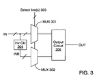
- FIG. 3 is a block diagram of a pseudo-differential multiplexer circuit according to one aspect of the present invention.
- the circuit includes two multiplexers (MUX 301 , 302 ), an inversion circuit 304 coupled between the input terminals of the two multiplexers, and an output circuit coupled to the output terminals of the two multiplexers.
- Inversion circuit 304 can also be considered as including two or more smaller inversion circuits, one inversion circuit being coupled between each corresponding pair of input terminals in the two multiplexers.
- the first multiplexer 301 and the inversion circuit are driven by a plurality of circuit input signals IN. (The slash mark across the IN signal line in FIG. 3 indicates that the line includes two or more input signals.)
- Both multiplexers are controlled by select line or lines 303 .
- Output circuit 305 provides signal OUT, an output signal for the pseudo-differential multiplexer circuit.
- Multiplexers 301 and 302 can be, for example, binary multiplexers (e.g., as shown in FIGS. 4–7 , 9 , and 11 ), or one-hot multiplexers (e.g., as shown in FIG. 10 ). Other multiplexer embodiments can also be used. Maximum benefit is derived from the invention when the multiplexers include only N-channel transistors on each path between the input terminals and the output terminal of each multiplexer. Importantly, the select terminals of the two multiplexers are coupled such that the two multiplexers are configured to select a corresponding one of their respective input signals in response to equivalent signals received at their respective select input terminals.
- Inversion circuit 304 can be implemented, for example, as an inverter coupled between each pair of multiplexer input terminals (e.g., as in the embodiment of FIG. 4 ), or as part of a memory cell providing true and complement output signals (as in the embodiment of FIG. 11 ).
- the complementary input signals driving multiplexer 302 are strict inversions of the corresponding circuit input signals driving multiplexer 301 . (In other words, each complementary input signal always has an opposite value to the corresponding circuit input signal.)
- inversion circuit 304 is implemented as a pulldown gated by the corresponding circuit input signal (e.g., as in the embodiments of FIGS. 5–7 and 9 – 10 ).
- Inversion circuit 304 can also be implemented in other ways (not shown).
- Output circuit 305 can also be implemented in various ways, as shown in the various examples illustrated herein. Output circuit 305 can also be implemented in other ways (not shown). No matter what the values of the circuit input signals, at least one of the two multiplexers always provides a low value. Therefore, there is no need for a reduced high value (VDD-Vth) to flip an inverter in the output circuit.
- VDD-Vth reduced high value
- FIG. 4 illustrates a first embodiment of the pseudo-differential multiplexer circuit of FIG. 3 .
- Multiplexer 301 is implemented as a standard binary multiplexer 301 a , as described in connection with FIG. 1 , and provides signal INT 6 .
- Multiplexer 302 is implemented as another standard binary multiplexer 302 a and includes N-channel transistors 400 – 407 , 410 – 413 , and 420 – 421 , coupled together in the same fashion as N-channel transistors 100 – 107 , 110 – 113 , and 120 – 121 , respectively.
- Multiplexer 302 a provides signal INT 7 .
- the select terminals of the two multiplexers are driven by select signals S 0 –S 2 and inverters 141 – 143 , as in the circuit of FIG. 1 .
- Inversion circuit 304 is implemented as shown in circuit 304 a , which includes eight inverters 450 – 457 coupled between the circuit input signals IN 0 –IN 7 and the corresponding input terminals of multiplexer 302 a.
- Output circuit 305 is implemented as shown in output circuit 305 a , which includes a pair of cross-coupled inverters 431 and 432 . Note that either inverter can drive the output node (i.e., either signal OUT 1 or signal OUT 2 can provide the circuit output signal OUT shown in FIG. 3 ). The selection can be made, for example, based on the desired sense of the output signal. Some embodiments (not shown) include an additional inverter coupled to the selected output terminal and providing additional buffering.
- multiplexers 301 a and 302 a are limited to the range between zero volts (ground, or GND) and VDD-Vth (one N-channel threshold below power high VDD). Because the voltage swing is smaller, for example, than in the CMOS multiplexer illustrated in FIG. 2 , multiplexers 301 a and 302 a together have a lower power dissipation. The leakage current is also reduced relative to the circuit of FIG. 2 .
- FIG. 5 illustrates a second embodiment of the pseudo-differential multiplexer circuit of FIG. 3 .
- the circuit of FIG. 5 is similar to that of FIG. 4 , except for the implementation of inversion circuit 304 .
- Inversion circuit 304 of FIG. 3 is implemented as shown in circuit 304 b of FIG. 5 , which includes eight pulldowns 550 – 557 coupled between the eight multiplexer input terminals and a ground terminal GND.
- a high value on one of the circuit input terminals IN 0 –IN 7 pulls down the corresponding input terminal of the second multiplexer.
- the second multiplexer passes a low value capable of flipping inverter 431 , thereby providing a high value at output terminal OUT 2 and a low value at terminal OUT 1 .
- FIG. 6 illustrates a third embodiment of the pseudo-differential multiplexer circuit of FIG. 3 .
- the circuit of FIG. 6 is similar to that of FIG. 5 , except for the implementation of output circuit 305 .
- Output circuit 305 of FIG. 3 is implemented as shown in circuit 305 b in FIG. 6 .
- Output circuit 305 b includes an inverter 633 driven by the output INT 6 of the first multiplexer and providing output signal OUT, as well as two pullups 631 , 632 .
- pullup 631 is a P-channel transistor coupled between the output terminal INT 7 of the second multiplexer and a power high terminal VDD, and gated by the output INT 6 of the first multiplexer.
- Pullup 632 is a P-channel transistor coupled between the output terminal of the first multiplexer and a power high terminal VDD, and gated by the output of the second multiplexer.
- FIG. 7 illustrates a fourth embodiment of the pseudo-differential multiplexer circuit of FIG. 3 .
- the circuit of FIG. 7 is similar to those of FIGS. 5 and 6 , except for the implementation of output circuit 305 .
- Output circuit 305 of FIG. 3 is implemented as shown in circuit 305 c in FIG. 7 .
- Output circuit 305 c includes an inverter 732 having an input terminal driven by the output INT 7 of the second multiplexer and an output terminal coupled to the output INT 6 of the first multiplexer.
- Output circuit 305 c also includes a pullup 731 .
- pullup 731 is a P-channel transistor coupled between the output terminal INT 7 of the second multiplexer and a power high terminal VDD, and gated by the output INT 6 of the first multiplexer.
- the output signals of the various multiplexer circuits illustrated herein do not always have the same sense.
- the multiplexer circuits of FIGS. 1 , 2 , and 6 are inverting circuits, while the output signals from FIGS. 3–5 can be of either sense.
- the multiplexer circuit illustrated in FIG. 7 provides a non-inverted output value.
- the circuit output signals of any of the illustrated or described embodiments are easily inverted as desired by one of skill in the art.
- Circuits that can particularly benefit from the invention include, for example, programmable logic devices (PLDs), which typically include a very large number of multiplexer circuits.
- PLDs programmable logic devices
- Programmable logic devices are a well-known type of integrated circuit that can be programmed to perform specified logic functions.
- FIG. 8 is a simplified illustration of one type of PLD, the Field Programmable Gate Array (FPGA).
- the FPGA of FIG. 8 includes an array of configurable logic blocks (LBs 801 a – 801 i ) and programmable input/output blocks (I/Os 802 a – 802 d ).
- the LBs and I/O blocks are interconnected by a programmable interconnect structure that includes a large number of interconnect lines 803 interconnected by programmable interconnect points (PIPs 804 , shown as small circles in FIG. 8 ).
- PIPs are often coupled into groups (e.g., group 805 ) that implement multiplexer circuits (routing multiplexers) selecting one of several interconnect lines to provide a signal to a destination interconnect line or logic block.
- Configurable logic blocks often include lookup tables (LUT), addressable memory arrays that provide any function of a limited number of input signal values.
- Lookup tables are typically implemented using memory cells and a multiplexer.
- the memory cells store predetermined values, while the multiplexer uses the input signals to select one of the predetermined values from among the stored contents of the memory cells.
- the multiplexer circuit of FIG. 1 can be used to implement a PLD LUT, where the input signals IN 0 –IN 7 are provided by memory cells.
- a LUT typically has 16 input signals, and this larger structure is easily extrapolated from the circuit of FIG. 1 by doubling the number of input signals and adding another stage to the multiplexer circuit.
- the interconnect structure and logic blocks of an FPGA are typically programmed by loading a stream of configuration data into internal configuration memory cells that define how the logic blocks and interconnect are configured.
- These configuration memory cells can include, for example, the memory cells described above in relation to the routing multiplexers and LUTs.
- the configuration data can be read from memory (e.g., an external PROM) or written into the FPGA by an external device. The collective states of the individual memory cells then determine the function of the FPGA.
- FIG. 9 shows one way in which the invention can be used to implement a routing multiplexer for a PLD.
- the circuit of FIG. 9 can be used, for example, to implement multiplexer 805 of FIG. 8 .
- the input signals are provided by eight interconnect lines IL 0 –IL 7 included in the interconnect structure of the PLD.
- Three configuration memory cells RM 0 –RM 2 provide stored values that programmably select one of the eight input signals from interconnect lines IL 0 –IL 7 .
- the routing multiplexer is implemented in a pseudo-differential manner similar to that of FIG. 7 . Thus, both high and low values from the interconnect lines are properly passed to output node OUT irregardless of a voltage drop applied to a high signal value.
- routing multiplexer can be the same as, smaller than, or larger than eight. In modern PLDS, for example, routing multiplexers often select from more than eight input signals. However, differently sized routing multiplexers can easily be extrapolated from the illustrated examples by one of skill in the relevant arts, as is the case for all of the exemplary circuits shown in the figures herein.
- FIG. 10 illustrates another way in which the invention can be used to implement a routing multiplexer for a PLD.
- the circuit of FIG. 10 can be used, for example, to implement multiplexer 805 of FIG. 8 .
- the embodiment of FIG. 10 utilizes one-hot encoding, rather than binary encoding, for the two multiplexers 301 b and 302 b .
- routing multiplexers often have other numbers of input signals than eight, but an 8-to-1 multiplexer is illustrated, for simplicity and consistency with the other figures herein.
- multiplexer 301 of FIG. 3 is implemented as shown in circuit 301 b .
- Circuit 301 b includes one N-channel transistor 1010 – 1017 for each input signal IL 0 –IL 7 , and provides signal INT 106 .
- circuit 302 b includes one N-channel transistor 1000 – 1007 for each input signal, and provides signal INT 107 .
- Eight configuration memory cells R 0 –R 7 are provided, each controlling one N-channel transistor in each multiplexer.
- only one of the eight configuration memory cells R 0 –R 7 can provide a high value at any given time, to avoid possible contention at intermediate nodes INT 106 and INT 107 .
- FIG. 11 shows one way in which the invention can be used to implement a lookup table (LUT) for a PLD.
- the circuit of FIG. 11 can be used, for example, in logic blocks (LBs) 801 a – 801 i of FIG. 8 .
- the input signals are provided by eight configuration memory cells M 0 –M 7 .
- the three select signals are provided by interconnect lines L 0 –L 2 included in the interconnect structure of the PLD.
- the three input signals L 0 –L 2 programmably select one of the eight stored values from memory cells M 0 –M 7 .
- many LUTs include 16 input signals and four select signals, for example. This and many other variations are easily extrapolated from the examples illustrated herein, as previously described.
- the LUT of FIG. 11 is implemented in a pseudo-differential manner similar to that of FIG. 4 , for example.
- both high and low values from the interconnect lines are properly passed to output node OUT irregardless of a voltage drop applied to a high signal value.
- the output circuit of FIG. 7 is utilized in the pictured embodiment, although other implementations can also be used.
- the multiplexers can also be implemented using one-hot encoding as in FIG. 10 , or in some other manner. It will be apparent to one skilled in the art after reading this specification that the present invention can be practiced within these and other architectural variations.
- each memory cell M 0 –M 7 provides both true and complement values of the stored contents of the memory cell. Thus, an additional inversion circuit is not needed.
- FIG. 12 illustrates the steps of a method of selecting one from a plurality of circuit input signals, according to an aspect of the present invention.
- the method of FIG. 12 can be implemented, for example, by utilizing any of the circuits illustrated in FIGS. 3–7 and 9 – 11 .
- step 1201 two or more circuit input signals are provided to a first multiplexer.
- step 1202 complementary input signals are generated from the circuit input signals.
- Each complementary input signal has a first value (e.g., low) whenever a corresponding circuit input signal has a second value (e.g., high).
- the complementary input signals are strict inversions of the corresponding circuit input signals. In other words, each complementary input signal always has an opposite value to the corresponding circuit input signal.
- only the second value (e.g., high) on a circuit input signal causes the complementary signal to change to the first value (e.g., low), while the first value (e.g., low) on the circuit input signal is ignored.
- the complementary input signals are provided to a second input multiplexer.
- one of the circuit input signals is selected in the first multiplexer, and a corresponding one of the complementary input signals is selected in the second multiplexer.
- values stored in memory cells are used to control the selecting.
- One such embodiment for example, is a routing multiplexer in a PLD, and the memory cells are configuration memory cells of the PLD.
- the circuit input signals are stored in memory cells.
- the circuit implements a PLD lookup table, and the memory cells are configuration memory cells of the PLD.
- the selected signals are utilized to generate an output signal.
- circuits of the invention in the context of programmable logic devices (PLDs) such as FPGAs and CPLDs.
- PLDs programmable logic devices
- the circuits of the invention can also be implemented in other integrated circuits, including non-programmable circuits as well as PLDs other than FPGAs and CPLDs.
- the circuits of the invention can also be implemented in electronic systems other than integrated circuits, e.g., in printed circuit boards including discrete devices.
- pullups, pulldowns, transistors, P-channel transistors, N-channel transistors, multiplexers, inversion circuits, inverters, buffers, output circuits, latches, and other components other than those described herein can be used to implement the invention.
- Active-high signals can be replaced with active-low signals by making straightforward alterations to the circuitry, such as are well known in the art of circuit design.
- Logical circuits can be replaced by their logical equivalents by appropriately inverting input and output signals, as is also well known.
Abstract
Pseudo-differential multiplexer circuits and methods. The circuit input signals are provided to two similar multiplexers, one of which is driven by true signals and one by the complementary input signals. No matter what the values of the circuit input signals, at least one of the two multiplexers always selects a low value. Therefore, at least one of the two multiplexers has the capability of overcoming a value stored in an output circuit (e.g., a latch) coupled to the output terminals of the two multiplexers. Thus, even when neither multiplexer can provide a high signal at the full value of power high VDD, the output circuit provides the correct output value. The invention also encompasses methods of selecting between circuit input signals by utilizing a pseudo-differential multiplexing technique, e.g., utilizing multiplexer circuits similar to those described above.
Description
The invention relates to multiplexer circuits. More particularly, the invention relates to multiplexer circuits that utilize pseudo-differential input signals.
Multiplexer circuits are very common in integrated circuits (ICs) and other electronic circuits. For example, multiplexer circuits are used throughout many programmable logic devices (PLDs), such as field programmable gate arrays (FPGAs) and complex programmable logic devices (CPLDs), to programmably select one of several different input signals to pass to a logic destination, or to select one of several stored values to provide as the output signal from a lookup table (LUT). Therefore, multiplexers can form a significant portion of the logic circuitry in a PLD. Hence, reducing the power dissipation and/or the leakage current of these multiplexers can significantly improve the overall performance of an electronic device in these increasingly important areas.
The circuit of FIG. 1 includes 8 input terminals IN0–IN7, three select terminals S0–S2, an output terminal OUT, N-channel transistors 100–107, 110–113, and 120–121, inverters 141–143, and half-latch 130. Half-latch 130 includes inverter 131 and pullup 132. (In the present specification, the same reference characters are used to refer to terminals, signal lines, signal nodes, and their corresponding signals.)
A high value on select signal S0 passes signals IN7, IN5, IN3, and IN1 to internal nodes INT3, INT2, INT1, and INT0, respectively. A low value on select signal S0 is inverted by inverter 141 to provide a high signal that passes signals IN6, IN4, IN2, and IN0 to internal nodes INT3, INT2, INT1, and INT0, respectively. A high value on select signal S1 passes signals INT3 and INT1 to internal nodes INT5 and IN4, respectively. A low value on select signal S1 is inverted by inverter 142 to provide a high signal that passes signals INT2 and INT0 to internal nodes INT5 and INT4, respectively. A high value on select signal S2 passes signal INT5 to internal node INT6. A low value on select signal S2 is inverted by inverter 143 to provide a high signal that passes signal INT4 to internal node INT6.
A low value on internal node INT6 is inverted by inverter 131 and provides a high value (power high VDD) at the output terminal OUT. However, an N-channel transistor passes a high value with a voltage drop of one N-channel threshold voltage Vth from the gate voltage. Therefore, a high value passed to node INT6 equals not power high VDD, but VDD-Vth. At today's low operating voltages, this reduced high value may not fully turn off the pullup, or turn on the pulldown, included in inverter 131. Therefore, pullup 132 is provided on internal node INT6 to pull the node fully to VDD whenever output terminal OUT reaches a sufficiently low value to turn on the pullup. Thus, inverter 131 functions properly and leakage through the inverter is reduced.
The circuit of FIG. 1 works well with sufficiently high values of VDD. As long as the voltage level VDD-Vth is high enough to flip inverter 131 and turn on pullup 132, the circuit functions properly. However, power high voltage levels (VDD) are much lower in today's ICs than was previously the case. For example, when VDD=1.2 volts and Vth=0.5 volts, a voltage level of VDD−Vth=0.7 volts cannot be relied upon to flip inverter 131.
Various methods have been used to resolve this problem. One known method is to use a gate voltage higher than VDD when driving a high value onto the gates of N-channel transistors 100–107, 110–113, and 120–121 (i.e., signals S0–S2 and inverters 141–143 are implemented using a “pumped” power high voltage greater than VDD). For example, if the gate voltage is higher than VDD by one threshold voltage Vth, the resulting voltage at node INT6 is (VDD+Vth−Vth), or simply VDD. Another approach is to lower the threshold voltage of N-channel transistors 100–107, 110–113, and 120–121. However, each of these solutions complicates the fabrication of the circuit, especially at very short gate lengths. These solutions are becoming less viable as IC gate lengths become shorter and shorter, and VDD values lower and lower, with the passage of time.
An alternative solution to this problem is presented in FIG. 2 . As previously described, an N-channel transistor passes only a “degraded” (e.g., reduced) version of a high voltage value. However, a P-channel transistor passes high voltage values with no voltage degradation. Therefore, the voltage degradation can be eliminated by replacing the N-channel transistors with CMOS passgates, each of which includes a pair of N-channel and P-channel transistors coupled in parallel. The P-channel transistor is gated by the inverse signal of the associated N-channel transistor. The N-channel transistor provides a fast response to a high input signal, while the P-channel transistor pulls a high output value fully “to the rail”, i.e., all the way to VDD.
The multiplexer circuit of FIG. 2 is similar to the circuit of FIG. 1 , except that N-channel transistors 100–107, 110–113, and 120–121 are replaced by CMOS pass transistors 200–207, 210–213, and 220–221. The N-channel transistors are gated by the same signals as in FIG. 1 , and the P-channel transistors are gated by the inverted signals. Components unchanged from those of FIG. 1 are similarly numbered, and are not again described.
Note that the pullup 132 of FIG. 1 is not needed in the circuit of FIG. 2 , because a high value provided to node INT6 already has the full value of VDD.
However, the circuit of FIG. 2 also has its drawbacks. For example, a matrix of passgates that includes both N-channel and P-channel transistors (as in the circuit of FIG. 2 ) requires more than twice as much area to implement within an IC. This limitation is partially due to the fact that P-channel transistors are placed within an N-well in the substrate. The N-well consumes additional area, both in itself and in the extra spacing required to isolate the N-well from the N-channel transistors. Additionally, a P-channel transistor must be made about twice as wide as an N-channel transistor to provide the same speed of operation. Therefore, each P-channel transistor consumes much more area than the associated N-channel transistor.
Therefore, it is desirable to provide multiplexer circuits and methods that pass a full high value (i.e., VDD) to the circuit output node, but do not unduly complicate the fabrication process, and which consume less area than the CMOS solution illustrated in FIG. 2 .
The invention provides pseudo-differential multiplexer circuits and methods. The circuit input signals are provided to two similar multiplexers, one of which is driven by true signals and one by the complementary input signals. In some embodiments, the complementary input signals are strict inversions of the circuit input signals, wherein each complementary input signal always has an opposite value to the corresponding circuit input signal. In other embodiments, a given value (e.g., a high value) on a circuit input signal always forces another value (e.g., a low value) on the corresponding complementary input signal. However, another value (e.g., a low value) on the circuit input signal has no effect on the corresponding complementary input signal.
No matter what the values of the circuit input signals, at least one of the two multiplexers always selects a low value. Therefore, at least one of the two multiplexers has the capability of overcoming a value stored in an output circuit (e.g., a latch) coupled to the output terminals of the two multiplexers. Thus, even when neither multiplexer can provide a high signal at the full value of power high VDD, the output circuit provides the correct output value.
Therefore, the invention enables the use of multiplexers that include only N-channel transistors in the signal paths between the data input and output terminals, even at very low operating voltages. Power dissipation and leakage current are also lower than is normally achieved using traditional multiplexer circuits. Additionally, the layout area required to implement the resulting structures is less than is required for traditional CMOS implementations.
The invention also encompasses methods of selecting between circuit input signals by utilizing a pseudo-differential multiplexing technique, e.g., utilizing multiplexer circuits similar to those described above.
The present invention is illustrated by way of example, and not by way of limitation, in the following figures.
In the following description, numerous specific details are set forth to provide a more thorough understanding of the present invention. However, it will be apparent to one skilled in the art that the present invention can be practiced without these specific details.
Note that the voltage within multiplexers 301 a and 302 a is limited to the range between zero volts (ground, or GND) and VDD-Vth (one N-channel threshold below power high VDD). Because the voltage swing is smaller, for example, than in the CMOS multiplexer illustrated in FIG. 2 , multiplexers 301 a and 302 a together have a lower power dissipation. The leakage current is also reduced relative to the circuit of FIG. 2 .
Note that the output signals of the various multiplexer circuits illustrated herein do not always have the same sense. For example, the multiplexer circuits of FIGS. 1 , 2, and 6 are inverting circuits, while the output signals from FIGS. 3–5 can be of either sense. The multiplexer circuit illustrated in FIG. 7 , on the other hand, provides a non-inverted output value. However, the circuit output signals of any of the illustrated or described embodiments are easily inverted as desired by one of skill in the art.
Many electronic circuits and systems can benefit by including the pseudo-differential multiplexer circuits described herein. Circuits that can particularly benefit from the invention include, for example, programmable logic devices (PLDs), which typically include a very large number of multiplexer circuits. Programmable logic devices (PLDs) are a well-known type of integrated circuit that can be programmed to perform specified logic functions.
Configurable logic blocks often include lookup tables (LUT), addressable memory arrays that provide any function of a limited number of input signal values. Lookup tables are typically implemented using memory cells and a multiplexer. The memory cells store predetermined values, while the multiplexer uses the input signals to select one of the predetermined values from among the stored contents of the memory cells. For example, the multiplexer circuit of FIG. 1 can be used to implement a PLD LUT, where the input signals IN0–IN7 are provided by memory cells. A LUT typically has 16 input signals, and this larger structure is easily extrapolated from the circuit of FIG. 1 by doubling the number of input signals and adding another stage to the multiplexer circuit.
The interconnect structure and logic blocks of an FPGA are typically programmed by loading a stream of configuration data into internal configuration memory cells that define how the logic blocks and interconnect are configured. These configuration memory cells can include, for example, the memory cells described above in relation to the routing multiplexers and LUTs. The configuration data can be read from memory (e.g., an external PROM) or written into the FPGA by an external device. The collective states of the individual memory cells then determine the function of the FPGA.
Note that the number of input signals and select signals in a PLD routing multiplexer can be the same as, smaller than, or larger than eight. In modern PLDS, for example, routing multiplexers often select from more than eight input signals. However, differently sized routing multiplexers can easily be extrapolated from the illustrated examples by one of skill in the relevant arts, as is the case for all of the exemplary circuits shown in the figures herein.
In the embodiment of FIG. 10 , multiplexer 301 of FIG. 3 is implemented as shown in circuit 301 b. Circuit 301 b includes one N-channel transistor 1010–1017 for each input signal IL0–IL7, and provides signal INT106. Similarly, circuit 302 b includes one N-channel transistor 1000–1007 for each input signal, and provides signal INT107. Eight configuration memory cells R0–R7 are provided, each controlling one N-channel transistor in each multiplexer. As indicated by the “one-hot” designation for multiplexers 301 b and 302 b, only one of the eight configuration memory cells R0–R7 can provide a high value at any given time, to avoid possible contention at intermediate nodes INT106 and INT107.
The LUT of FIG. 11 is implemented in a pseudo-differential manner similar to that of FIG. 4 , for example. Thus, both high and low values from the interconnect lines are properly passed to output node OUT irregardless of a voltage drop applied to a high signal value. Note that the output circuit of FIG. 7 is utilized in the pictured embodiment, although other implementations can also be used. The multiplexers can also be implemented using one-hot encoding as in FIG. 10 , or in some other manner. It will be apparent to one skilled in the art after reading this specification that the present invention can be practiced within these and other architectural variations.
Note that in the embodiment of FIG. 11 the inversion circuit is not illustrated. Instead, each memory cell M0–M7 provides both true and complement values of the stored contents of the memory cell. Thus, an additional inversion circuit is not needed.
In step 1201, two or more circuit input signals are provided to a first multiplexer. In step 1202, complementary input signals are generated from the circuit input signals. Each complementary input signal has a first value (e.g., low) whenever a corresponding circuit input signal has a second value (e.g., high). In some embodiments, the complementary input signals are strict inversions of the corresponding circuit input signals. In other words, each complementary input signal always has an opposite value to the corresponding circuit input signal. In some embodiments, only the second value (e.g., high) on a circuit input signal causes the complementary signal to change to the first value (e.g., low), while the first value (e.g., low) on the circuit input signal is ignored. In step 1203, the complementary input signals are provided to a second input multiplexer.
In step 1204, one of the circuit input signals is selected in the first multiplexer, and a corresponding one of the complementary input signals is selected in the second multiplexer. In some embodiments, values stored in memory cells are used to control the selecting. One such embodiment, for example, is a routing multiplexer in a PLD, and the memory cells are configuration memory cells of the PLD. In some embodiments, the circuit input signals are stored in memory cells. In one such embodiment, the circuit implements a PLD lookup table, and the memory cells are configuration memory cells of the PLD. In step 1205, the selected signals are utilized to generate an output signal.
Those having skill in the relevant arts of the invention will now perceive various modifications and additions that can be made as a result of the disclosure herein. For example, the above text describes the circuits of the invention in the context of programmable logic devices (PLDs) such as FPGAs and CPLDs. However, the circuits of the invention can also be implemented in other integrated circuits, including non-programmable circuits as well as PLDs other than FPGAs and CPLDs. The circuits of the invention can also be implemented in electronic systems other than integrated circuits, e.g., in printed circuit boards including discrete devices.
Further, pullups, pulldowns, transistors, P-channel transistors, N-channel transistors, multiplexers, inversion circuits, inverters, buffers, output circuits, latches, and other components other than those described herein can be used to implement the invention. Active-high signals can be replaced with active-low signals by making straightforward alterations to the circuitry, such as are well known in the art of circuit design. Logical circuits can be replaced by their logical equivalents by appropriately inverting input and output signals, as is also well known.
Moreover, some components are shown directly connected to one another while others are shown connected via intermediate components. In each instance, the method of interconnection establishes some desired electrical communication between two or more circuit nodes. Such communication can often be accomplished using a number of circuit configurations, as will be understood by those of skill in the art.
Accordingly, all such modifications and additions are deemed to be within the scope of the invention, which is to be limited only by the appended claims and their equivalents.
Claims (13)
1. A multiplexer circuit, comprising:
a first plurality of circuit input terminals providing a first plurality of input signals;
a second plurality of circuit input terminals providing a second plurality of input signals having complementary values to the first plurality of input signals;
a circuit output terminal;
a first multiplexer having a plurality of input terminals coupled to the first plurality of circuit input terminals, at least one select terminal, and an output terminal;
a second multiplexer having a plurality of input terminals coupled to the second plurality of circuit input terminals, at least one select terminal coupled to the at least one select terminal of the first multiplexer, and an output terminal;
an output circuit having a first input terminal coupled to the output terminal of the first multiplexer, a second input terminal coupled to the output terminal of the second multiplexer, and an output terminal coupled to the circuit output terminal; and
a plurality of inversion circuits, each inversion circuit being coupled between one of the first circuit input terminals and a corresponding one of the second circuit input terminals, each inversion circuit comprising a memory cell,
wherein the first and second multiplexers are configured to select a corresponding one of their respective input terminals in response to equivalent signals received at their respective select terminals.
2. The multiplexer circuit of claim 1 , wherein each of the inversion circuits further comprises an inverter.
3. The multiplexer circuit of claim 1 , wherein each memory cell comprises a true output terminal coupled to one of the first plurality of circuit input terminals and a complement output terminal coupled to a corresponding one of the second plurality of circuit input terminals.
4. The multiplexer circuit of claim 1 , further comprising at least one memory cell coupled to the select terminals of the first and second multiplexers.
5. The multiplexer circuit of claim 1 , wherein:
each of the first and second multiplexers comprises a plurality of select terminals comprising select terminal pairs; and
the multiplexer circuit further comprises, for each select terminal pair, an inverter coupled between the two select terminals comprising the pair.
6. The multiplexer circuit of claim 1 , wherein the output circuit comprises a latch.
7. The multiplexer circuit of claim 6 , wherein the latch comprises first and second cross-coupled inverters.
8. The multiplexer circuit of claim 1 , wherein the output circuit comprises:
an inverter having an input terminal coupled to the output terminal of the first multiplexer and an output terminal coupled to the circuit output terminal;
a first pullup coupled between the output terminal of the first multiplexer and a power high terminal, the first pullup having a gate terminal coupled to the output terminal of the second multiplexer; and
a second pullup coupled between the output terminal of the second multiplexer and the power high terminal, the second pullup having a gate terminal coupled to the output terminal of the first multiplexer.
9. The multiplexer circuit of claim 1 , wherein the output circuit comprises:
an inverter having an input terminal coupled to the output terminal of the second multiplexer and an output terminal coupled to the output terminal of the first multiplexer; and
a P-channel transistor coupled between the output terminal of the second multiplexer and a power high terminal, the P-channel transistor having a gate terminal coupled to the output terminal of the first multiplexer and further coupled to the circuit output terminal.
10. The multiplexer circuit of claim 1 , wherein the first and second pluralities of circuit input terminals each comprise eight input terminals.
11. The multiplexer circuit of claim 1 , wherein the first and second multiplexers each comprise a plurality of transistors coupled in series between their respective input and output terminals, and all of the transistors consist of N-channel transistors.
12. The multiplexer circuit of claim 1 , wherein the first and second multiplexers comprise binary multiplexers.
13. The multiplexer circuit of claim 1 , wherein the first and second multiplexers comprise one-hot multiplexers.
Priority Applications (2)
| Application Number | Priority Date | Filing Date | Title |
|---|---|---|---|
| US10/796,330 US6992505B1 (en) | 2004-03-09 | 2004-03-09 | Structures and methods of implementing a pass gate multiplexer with pseudo-differential input signals |
| US11/235,898 US7046041B1 (en) | 2004-03-09 | 2005-09-27 | Structures and methods of implementing a pass gate multiplexer with pseudo-differential input signals |
Applications Claiming Priority (1)
| Application Number | Priority Date | Filing Date | Title |
|---|---|---|---|
| US10/796,330 US6992505B1 (en) | 2004-03-09 | 2004-03-09 | Structures and methods of implementing a pass gate multiplexer with pseudo-differential input signals |
Related Child Applications (1)
| Application Number | Title | Priority Date | Filing Date |
|---|---|---|---|
| US11/235,898 Division US7046041B1 (en) | 2004-03-09 | 2005-09-27 | Structures and methods of implementing a pass gate multiplexer with pseudo-differential input signals |
Publications (1)
| Publication Number | Publication Date |
|---|---|
| US6992505B1 true US6992505B1 (en) | 2006-01-31 |
Family
ID=35694853
Family Applications (2)
| Application Number | Title | Priority Date | Filing Date |
|---|---|---|---|
| US10/796,330 Expired - Lifetime US6992505B1 (en) | 2004-03-09 | 2004-03-09 | Structures and methods of implementing a pass gate multiplexer with pseudo-differential input signals |
| US11/235,898 Expired - Lifetime US7046041B1 (en) | 2004-03-09 | 2005-09-27 | Structures and methods of implementing a pass gate multiplexer with pseudo-differential input signals |
Family Applications After (1)
| Application Number | Title | Priority Date | Filing Date |
|---|---|---|---|
| US11/235,898 Expired - Lifetime US7046041B1 (en) | 2004-03-09 | 2005-09-27 | Structures and methods of implementing a pass gate multiplexer with pseudo-differential input signals |
Country Status (1)
| Country | Link |
|---|---|
| US (2) | US6992505B1 (en) |
Cited By (63)
| Publication number | Priority date | Publication date | Assignee | Title |
|---|---|---|---|---|
| US7116131B1 (en) * | 2004-09-15 | 2006-10-03 | Xilinx, Inc. | High performance programmable logic devices utilizing dynamic circuitry |
| US7126373B1 (en) | 2004-02-14 | 2006-10-24 | Herman Schmit | Configurable logic circuits with commutative properties |
| US7126381B1 (en) | 2004-02-14 | 2006-10-24 | Herman Schmit | VPA interconnect circuit |
| US7145361B1 (en) | 2004-06-30 | 2006-12-05 | Andre Rohe | Configurable integrated circuit with different connection schemes |
| US7157933B1 (en) | 2004-02-14 | 2007-01-02 | Herman Schmit | Configurable circuits, IC's, and systems |
| US7167025B1 (en) * | 2004-02-14 | 2007-01-23 | Herman Schmit | Non-sequentially configurable IC |
| US7193438B1 (en) | 2004-06-30 | 2007-03-20 | Andre Rohe | Configurable integrated circuit with offset connection |
| US7193432B1 (en) | 2004-02-14 | 2007-03-20 | Herman Schmit | VPA logic circuits |
| US7193440B1 (en) | 2004-02-14 | 2007-03-20 | Herman Schmit | Configurable circuits, IC's, and systems |
| US20070075737A1 (en) * | 2004-02-14 | 2007-04-05 | Herman Schmit | Configurable Circuits, IC's, and Systems |
| US7224181B1 (en) | 2004-11-08 | 2007-05-29 | Herman Schmit | Clock distribution in a configurable IC |
| US7224182B1 (en) | 2005-03-15 | 2007-05-29 | Brad Hutchings | Hybrid configurable circuit for a configurable IC |
| US7242216B1 (en) | 2004-11-08 | 2007-07-10 | Herman Schmit | Embedding memory between tile arrangement of a configurable IC |
| US7259587B1 (en) | 2004-11-08 | 2007-08-21 | Tabula, Inc. | Configurable IC's with configurable logic resources that have asymetric inputs and/or outputs |
| US7268586B1 (en) | 2004-11-08 | 2007-09-11 | Tabula, Inc. | Method and apparatus for accessing stored data in a reconfigurable IC |
| US7276933B1 (en) | 2004-11-08 | 2007-10-02 | Tabula, Inc. | Reconfigurable IC that has sections running at different looperness |
| US7282950B1 (en) | 2004-11-08 | 2007-10-16 | Tabula, Inc. | Configurable IC's with logic resources with offset connections |
| US7284222B1 (en) | 2004-06-30 | 2007-10-16 | Tabula, Inc. | Method and apparatus for identifying connections between configurable nodes in a configurable integrated circuit |
| US20070244959A1 (en) * | 2005-03-15 | 2007-10-18 | Steven Teig | Configurable IC's with dual carry chains |
| US20070241787A1 (en) * | 2004-06-30 | 2007-10-18 | Herman Schmit | Configurable Circuits, IC's, and Systems |
| US20070241781A1 (en) * | 2005-03-15 | 2007-10-18 | Brad Hutchings | Variable width management for a memory of a configurable IC |
| US20070241782A1 (en) * | 2004-11-08 | 2007-10-18 | Steven Teig | Configurable IC with interconnect circuits that also perform storage operations |
| US20070241776A1 (en) * | 2004-06-30 | 2007-10-18 | Herman Schmit | Configurable Logic Circuits with Commutative Properties |
| US20070241788A1 (en) * | 2004-06-30 | 2007-10-18 | Herman Schmit | VPA Logic Circuits |
| US20070241784A1 (en) * | 2005-03-15 | 2007-10-18 | Brad Hutchings | Configurable ic with interconnect circuits that have select lines driven by user signals |
| US20070241773A1 (en) * | 2005-03-15 | 2007-10-18 | Brad Hutchings | Hybrid logic/interconnect circuit in a configurable ic |
| US20070244961A1 (en) * | 2004-11-08 | 2007-10-18 | Herman Schmit | Configurable IC with configurable routing resources that have asymmetric Input and/or outputs |
| US20070257700A1 (en) * | 2005-03-15 | 2007-11-08 | Andrew Caldwell | Method and apparatus for decomposing functions in a configurable IC |
| US7295037B2 (en) | 2004-11-08 | 2007-11-13 | Tabula, Inc. | Configurable IC with routing circuits with offset connections |
| US7301368B2 (en) | 2005-03-15 | 2007-11-27 | Tabula, Inc. | Embedding memory within tile arrangement of a configurable IC |
| US7312630B2 (en) | 2004-06-30 | 2007-12-25 | Tabula, Inc. | Configurable integrated circuit with built-in turns |
| US7317331B2 (en) | 2004-11-08 | 2008-01-08 | Tabula, Inc. | Reconfigurable IC that has sections running at different reconfiguration rates |
| US7330050B2 (en) | 2004-11-08 | 2008-02-12 | Tabula, Inc. | Storage elements for a configurable IC and method and apparatus for accessing data stored in the storage elements |
| US7368946B1 (en) | 2006-06-16 | 2008-05-06 | Xilinx, Inc. | Level-shifting pass gate multiplexer |
| US7425841B2 (en) | 2004-02-14 | 2008-09-16 | Tabula Inc. | Configurable circuits, IC's, and systems |
| US20080231318A1 (en) * | 2007-03-20 | 2008-09-25 | Herman Schmit | Configurable ic having a routing fabric with storage elements |
| US7477073B1 (en) | 2006-06-16 | 2009-01-13 | Xilinx, Inc. | Structures and methods for heterogeneous low power programmable logic device |
| US20090146689A1 (en) * | 2007-09-06 | 2009-06-11 | Trevis Chandler | Configuration Context Switcher with a Clocked Storage Element |
| US20090327987A1 (en) * | 2008-06-26 | 2009-12-31 | Steven Teig | Timing operations in an IC with configurable circuits |
| US7653891B1 (en) * | 2007-02-23 | 2010-01-26 | Xilinx, Inc. | Method of reducing power of a circuit |
| US7669097B1 (en) | 2006-03-27 | 2010-02-23 | Tabula, Inc. | Configurable IC with error detection and correction circuitry |
| US7679401B1 (en) | 2005-12-01 | 2010-03-16 | Tabula, Inc. | User registers implemented with routing circuits in a configurable IC |
| US7694083B1 (en) | 2006-03-08 | 2010-04-06 | Tabula, Inc. | System and method for providing a virtual memory architecture narrower and deeper than a physical memory architecture |
| US20100085076A1 (en) * | 2007-01-05 | 2010-04-08 | Nxp, B.V. | Circuit comprising a matrix of programmable logic cells |
| US7743085B2 (en) | 2004-11-08 | 2010-06-22 | Tabula, Inc. | Configurable IC with large carry chains |
| US7765249B1 (en) | 2005-11-07 | 2010-07-27 | Tabula, Inc. | Use of hybrid interconnect/logic circuits for multiplication |
| US7797497B1 (en) | 2006-03-08 | 2010-09-14 | Tabula, Inc. | System and method for providing more logical memory ports than physical memory ports |
| US7804730B2 (en) | 2005-03-15 | 2010-09-28 | Tabula, Inc. | Method and apparatus for accessing contents of memory cells |
| US7818361B1 (en) | 2005-11-07 | 2010-10-19 | Tabula, Inc. | Method and apparatus for performing two's complement multiplication |
| US7898291B2 (en) | 2004-12-01 | 2011-03-01 | Tabula, Inc. | Operational time extension |
| US7917559B2 (en) | 2004-11-08 | 2011-03-29 | Tabula, Inc. | Configurable IC's with configurable logic circuits that perform adder and/or subtractor operations |
| US7930666B1 (en) | 2006-12-12 | 2011-04-19 | Tabula, Inc. | System and method of providing a memory hierarchy |
| US7971172B1 (en) | 2005-11-07 | 2011-06-28 | Tabula, Inc. | IC that efficiently replicates a function to save logic and routing resources |
| US20110221471A1 (en) * | 2008-09-17 | 2011-09-15 | Jason Redgrave | Controllable storage elements for an ic |
| US8112468B1 (en) | 2007-03-22 | 2012-02-07 | Tabula, Inc. | Method and apparatus for performing an operation with a plurality of sub-operations in a configurable IC |
| US8463836B1 (en) | 2005-11-07 | 2013-06-11 | Tabula, Inc. | Performing mathematical and logical operations in multiple sub-cycles |
| US8760193B2 (en) | 2011-07-01 | 2014-06-24 | Tabula, Inc. | Configurable storage elements |
| US8863067B1 (en) | 2008-02-06 | 2014-10-14 | Tabula, Inc. | Sequential delay analysis by placement engines |
| US8912820B2 (en) | 2010-04-02 | 2014-12-16 | Tabula, Inc. | System and method for reducing reconfiguration power |
| US8984464B1 (en) | 2011-11-21 | 2015-03-17 | Tabula, Inc. | Detailed placement with search and repair |
| US9148151B2 (en) | 2011-07-13 | 2015-09-29 | Altera Corporation | Configurable storage elements |
| US9203397B1 (en) | 2011-12-16 | 2015-12-01 | Altera Corporation | Delaying start of user design execution |
| US9543950B2 (en) * | 2014-07-21 | 2017-01-10 | Lattice Semiconductor Corporation | High speed complementary NMOS LUT logic |
Families Citing this family (1)
| Publication number | Priority date | Publication date | Assignee | Title |
|---|---|---|---|---|
| US8130044B2 (en) * | 2008-06-19 | 2012-03-06 | Altera Corporation | Phase-locked loop circuitry with multiple voltage-controlled oscillators |
Citations (4)
| Publication number | Priority date | Publication date | Assignee | Title |
|---|---|---|---|---|
| US6084437A (en) * | 1995-09-22 | 2000-07-04 | Kawasaki Steel Corporation | Logic circuit utilizing pass transistors and logic gate |
| US6121797A (en) * | 1996-02-01 | 2000-09-19 | Samsung Electronics Co., Ltd. | Energy economized pass-transistor logic circuit and full adder using the same |
| US6232799B1 (en) * | 1999-10-04 | 2001-05-15 | International Business Machines Corporation | Method and apparatus for selectively controlling weak feedback in regenerative pass gate logic circuits |
| US6768338B1 (en) * | 2003-01-30 | 2004-07-27 | Xilinx, Inc. | PLD lookup table including transistors of more than one oxide thickness |
Family Cites Families (1)
| Publication number | Priority date | Publication date | Assignee | Title |
|---|---|---|---|---|
| US6529040B1 (en) * | 2000-05-05 | 2003-03-04 | Xilinx, Inc. | FPGA lookup table with speed read decoder |
-
2004
- 2004-03-09 US US10/796,330 patent/US6992505B1/en not_active Expired - Lifetime
-
2005
- 2005-09-27 US US11/235,898 patent/US7046041B1/en not_active Expired - Lifetime
Patent Citations (4)
| Publication number | Priority date | Publication date | Assignee | Title |
|---|---|---|---|---|
| US6084437A (en) * | 1995-09-22 | 2000-07-04 | Kawasaki Steel Corporation | Logic circuit utilizing pass transistors and logic gate |
| US6121797A (en) * | 1996-02-01 | 2000-09-19 | Samsung Electronics Co., Ltd. | Energy economized pass-transistor logic circuit and full adder using the same |
| US6232799B1 (en) * | 1999-10-04 | 2001-05-15 | International Business Machines Corporation | Method and apparatus for selectively controlling weak feedback in regenerative pass gate logic circuits |
| US6768338B1 (en) * | 2003-01-30 | 2004-07-27 | Xilinx, Inc. | PLD lookup table including transistors of more than one oxide thickness |
Cited By (168)
| Publication number | Priority date | Publication date | Assignee | Title |
|---|---|---|---|---|
| US7872496B2 (en) | 2004-02-14 | 2011-01-18 | Tabula, Inc. | Method of mapping a user design defined for a user design cycle to an IC with multiple sub-cycle reconfigurable circuits |
| US7126373B1 (en) | 2004-02-14 | 2006-10-24 | Herman Schmit | Configurable logic circuits with commutative properties |
| US7126381B1 (en) | 2004-02-14 | 2006-10-24 | Herman Schmit | VPA interconnect circuit |
| US7425841B2 (en) | 2004-02-14 | 2008-09-16 | Tabula Inc. | Configurable circuits, IC's, and systems |
| US7157933B1 (en) | 2004-02-14 | 2007-01-02 | Herman Schmit | Configurable circuits, IC's, and systems |
| US7167025B1 (en) * | 2004-02-14 | 2007-01-23 | Herman Schmit | Non-sequentially configurable IC |
| US7532032B2 (en) | 2004-02-14 | 2009-05-12 | Tabula, Inc. | Configurable circuits, IC's, and systems |
| US7193432B1 (en) | 2004-02-14 | 2007-03-20 | Herman Schmit | VPA logic circuits |
| US7193440B1 (en) | 2004-02-14 | 2007-03-20 | Herman Schmit | Configurable circuits, IC's, and systems |
| US20070075737A1 (en) * | 2004-02-14 | 2007-04-05 | Herman Schmit | Configurable Circuits, IC's, and Systems |
| US8810277B2 (en) | 2004-02-14 | 2014-08-19 | Tbula, Inc. | Non-sequentially configurable IC |
| US20090160481A9 (en) * | 2004-02-14 | 2009-06-25 | Herman Schmit | Configurable Circuits, IC's and Systems |
| US20090167354A9 (en) * | 2004-02-14 | 2009-07-02 | Herman Schmit | Non-Sequentially Configurable IC |
| US8305110B2 (en) | 2004-02-14 | 2012-11-06 | Tabula, Inc. | Non-sequentially configurable IC |
| US7564260B1 (en) | 2004-02-14 | 2009-07-21 | Tabula Inc. | VPA interconnect circuit |
| US8193830B2 (en) | 2004-02-14 | 2012-06-05 | Tabula, Inc. | Configurable circuits, IC's, and systems |
| US7616027B2 (en) | 2004-02-14 | 2009-11-10 | Tabula, Inc. | Configurable circuits, IC's and systems |
| US7667486B2 (en) | 2004-02-14 | 2010-02-23 | Tabula, Inc. | Non-sequentially configurable IC |
| US20100219859A1 (en) * | 2004-02-14 | 2010-09-02 | Herman Schmit | Non-Sequentially Configurable IC |
| US20070241777A1 (en) * | 2004-02-14 | 2007-10-18 | Herman Schmit | Configurable Circuits, IC's and Systems |
| US20070241791A1 (en) * | 2004-02-14 | 2007-10-18 | Herman Schmit | Non-Sequentially Configurable IC |
| US7948266B2 (en) | 2004-02-14 | 2011-05-24 | Tabula, Inc. | Non-sequentially configurable IC |
| US8415973B2 (en) | 2004-06-30 | 2013-04-09 | Tabula, Inc. | Configurable integrated circuit with built-in turns |
| US20110202586A1 (en) * | 2004-06-30 | 2011-08-18 | Steven Teig | Configurable ic's with dual carry chains |
| US20070241789A1 (en) * | 2004-06-30 | 2007-10-18 | Andre Rohe | Configurable Integrated Circuit with Offset Connection |
| US20070241787A1 (en) * | 2004-06-30 | 2007-10-18 | Herman Schmit | Configurable Circuits, IC's, and Systems |
| US20070241788A1 (en) * | 2004-06-30 | 2007-10-18 | Herman Schmit | VPA Logic Circuits |
| US20110163781A1 (en) * | 2004-06-30 | 2011-07-07 | Andre Rohe | Method and apparatus for identifying connections between configurable nodes in a configurable integrated circuit |
| US20070241786A1 (en) * | 2004-06-30 | 2007-10-18 | Andre Rohe | Configurable Integrated Circuit with Different Connection Schemes |
| US7849434B2 (en) | 2004-06-30 | 2010-12-07 | Tabula, Inc. | Method and apparatus for identifying connections between configurable nodes in a configurable integrated circuit |
| US7839166B2 (en) | 2004-06-30 | 2010-11-23 | Tabula, Inc. | Configurable IC with logic resources with offset connections |
| US7994817B2 (en) | 2004-06-30 | 2011-08-09 | Tabula, Inc. | Configurable integrated circuit with built-in turns |
| US20070245287A1 (en) * | 2004-06-30 | 2007-10-18 | Andre Rohe | Method and apparatus for identifying connections between configurable nodes in a configurable integrated circuit |
| US20100210077A1 (en) * | 2004-06-30 | 2010-08-19 | Andre Rohe | Configurable integrated circuit with built-in turns |
| US7737722B2 (en) | 2004-06-30 | 2010-06-15 | Tabula, Inc. | Configurable integrated circuit with built-in turns |
| US7284222B1 (en) | 2004-06-30 | 2007-10-16 | Tabula, Inc. | Method and apparatus for identifying connections between configurable nodes in a configurable integrated circuit |
| US20080061823A1 (en) * | 2004-06-30 | 2008-03-13 | Herman Schmit | Configurable ic's with logic resources with offset connections |
| US20070241776A1 (en) * | 2004-06-30 | 2007-10-18 | Herman Schmit | Configurable Logic Circuits with Commutative Properties |
| US8281273B2 (en) | 2004-06-30 | 2012-10-02 | Tabula, Inc. | Method and apparatus for identifying connections between configurable nodes in a configurable integrated circuit |
| US8350591B2 (en) | 2004-06-30 | 2013-01-08 | Tabula, Inc. | Configurable IC's with dual carry chains |
| US20080129333A1 (en) * | 2004-06-30 | 2008-06-05 | Andre Rohe | Configurable Integrated Circuit with Built-in Turns |
| US7193438B1 (en) | 2004-06-30 | 2007-03-20 | Andre Rohe | Configurable integrated circuit with offset connection |
| US7312630B2 (en) | 2004-06-30 | 2007-12-25 | Tabula, Inc. | Configurable integrated circuit with built-in turns |
| US7468614B2 (en) | 2004-06-30 | 2008-12-23 | Tabula, Inc. | Configurable integrated circuit with offset connections |
| US7449915B2 (en) | 2004-06-30 | 2008-11-11 | Tabula Inc. | VPA logic circuits |
| US7439766B2 (en) | 2004-06-30 | 2008-10-21 | Tabula, Inc. | Configurable logic circuits with commutative properties |
| US7145361B1 (en) | 2004-06-30 | 2006-12-05 | Andre Rohe | Configurable integrated circuit with different connection schemes |
| US7408382B2 (en) | 2004-06-30 | 2008-08-05 | Tabula, Inc. | Configurable circuits, IC's, and systems |
| US20080059937A1 (en) * | 2004-06-30 | 2008-03-06 | Andre Rohe | Method and apparatus for identifying connections between configurable nodes in a configurable integrated circuit |
| US7382157B1 (en) | 2004-09-15 | 2008-06-03 | Xilinx, Inc. | Interconnect driver circuits for dynamic logic |
| US7116131B1 (en) * | 2004-09-15 | 2006-10-03 | Xilinx, Inc. | High performance programmable logic devices utilizing dynamic circuitry |
| US7656188B2 (en) | 2004-11-08 | 2010-02-02 | Tabula, Inc. | Reconfigurable IC that has sections running at different reconfiguration rates |
| US7917559B2 (en) | 2004-11-08 | 2011-03-29 | Tabula, Inc. | Configurable IC's with configurable logic circuits that perform adder and/or subtractor operations |
| US9048833B2 (en) | 2004-11-08 | 2015-06-02 | Tabula, Inc. | Storage elements for a configurable IC and method and apparatus for accessing data stored in the storage elements |
| US20080116931A1 (en) * | 2004-11-08 | 2008-05-22 | Herman Schmit | Embedding Memory within Tile Arrangement of a Configurable IC |
| US20080100339A1 (en) * | 2004-11-08 | 2008-05-01 | Herman Schmit | Configurable ic with routing circuits with offset connections |
| US7224181B1 (en) | 2004-11-08 | 2007-05-29 | Herman Schmit | Clock distribution in a configurable IC |
| US8698518B2 (en) | 2004-11-08 | 2014-04-15 | Tabula, Inc. | Storage elements for a configurable IC and method and apparatus for accessing data stored in the storage elements |
| US7342415B2 (en) * | 2004-11-08 | 2008-03-11 | Tabula, Inc. | Configurable IC with interconnect circuits that also perform storage operations |
| US20080164906A1 (en) * | 2004-11-08 | 2008-07-10 | Jason Redgrave | Storage Elements for a Configurable IC and Method and Apparatus for Accessing Data Stored in the Storage Elements |
| US20080180131A1 (en) * | 2004-11-08 | 2008-07-31 | Steven Teig | Configurable IC with Interconnect Circuits that also Perform Storage Operations |
| US20080036494A1 (en) * | 2004-11-08 | 2008-02-14 | Steven Teig | Reconfigurable ic that has sections running at different looperness |
| US7330050B2 (en) | 2004-11-08 | 2008-02-12 | Tabula, Inc. | Storage elements for a configurable IC and method and apparatus for accessing data stored in the storage elements |
| US7242216B1 (en) | 2004-11-08 | 2007-07-10 | Herman Schmit | Embedding memory between tile arrangement of a configurable IC |
| US7259587B1 (en) | 2004-11-08 | 2007-08-21 | Tabula, Inc. | Configurable IC's with configurable logic resources that have asymetric inputs and/or outputs |
| US7268586B1 (en) | 2004-11-08 | 2007-09-11 | Tabula, Inc. | Method and apparatus for accessing stored data in a reconfigurable IC |
| US20080030227A1 (en) * | 2004-11-08 | 2008-02-07 | Steven Teig | Reconfigurable IC that has Sections Running at Different Reconfiguration Rates |
| US20080018359A1 (en) * | 2004-11-08 | 2008-01-24 | Herman Schmit | Configurable IC's With Configurable Logic Resources That Have Asymmetric Inputs And/Or Outputs |
| US7317331B2 (en) | 2004-11-08 | 2008-01-08 | Tabula, Inc. | Reconfigurable IC that has sections running at different reconfiguration rates |
| US8248102B2 (en) | 2004-11-08 | 2012-08-21 | Tabula, Inc. | Configurable IC'S with large carry chains |
| US7276933B1 (en) | 2004-11-08 | 2007-10-02 | Tabula, Inc. | Reconfigurable IC that has sections running at different looperness |
| US8183882B2 (en) | 2004-11-08 | 2012-05-22 | Tabula, Inc. | Reconfigurable IC that has sections running at different reconfiguration rates |
| US8159264B2 (en) | 2004-11-08 | 2012-04-17 | Tabula, Inc. | Storage elements for a configurable IC and method and apparatus for accessing data stored in the storage elements |
| US20070285125A1 (en) * | 2004-11-08 | 2007-12-13 | Jason Redgrave | Method and Apparatus for Accessing Stored Data in a Reconfigurable IC |
| US7282950B1 (en) | 2004-11-08 | 2007-10-16 | Tabula, Inc. | Configurable IC's with logic resources with offset connections |
| US20070241774A1 (en) * | 2004-11-08 | 2007-10-18 | Steven Teig | Reconfigurable ic that has sections running at different looperness |
| US20110115523A1 (en) * | 2004-11-08 | 2011-05-19 | Jason Redgrave | Storage elements for a configurable ic and method and apparatus for accessing data stored in the storage elements |
| US20110031998A1 (en) * | 2004-11-08 | 2011-02-10 | Jason Redgrave | Configurable ic's with large carry chains |
| US20070241782A1 (en) * | 2004-11-08 | 2007-10-18 | Steven Teig | Configurable IC with interconnect circuits that also perform storage operations |
| US20070241778A1 (en) * | 2004-11-08 | 2007-10-18 | Herman Schmit | IC with configurable storage circuits |
| US20100007376A1 (en) * | 2004-11-08 | 2010-01-14 | Jason Redgrave | Storage elements for a configurable ic and method and apparatus for accessing data stored in the storage elements |
| US7825687B2 (en) | 2004-11-08 | 2010-11-02 | Tabula, Inc. | Storage elements for a configurable IC and method and apparatus for accessing data stored in the storage elements |
| US7652499B2 (en) | 2004-11-08 | 2010-01-26 | Tabula, Inc. | Embedding memory within tile arrangement of an integrated circuit |
| US7295037B2 (en) | 2004-11-08 | 2007-11-13 | Tabula, Inc. | Configurable IC with routing circuits with offset connections |
| US20070244961A1 (en) * | 2004-11-08 | 2007-10-18 | Herman Schmit | Configurable IC with configurable routing resources that have asymmetric Input and/or outputs |
| US7743085B2 (en) | 2004-11-08 | 2010-06-22 | Tabula, Inc. | Configurable IC with large carry chains |
| US8664974B2 (en) | 2004-12-01 | 2014-03-04 | Tabula, Inc. | Operational time extension |
| US20110181317A1 (en) * | 2004-12-01 | 2011-07-28 | Andre Rohe | Operational time extension |
| US7898291B2 (en) | 2004-12-01 | 2011-03-01 | Tabula, Inc. | Operational time extension |
| US7224182B1 (en) | 2005-03-15 | 2007-05-29 | Brad Hutchings | Hybrid configurable circuit for a configurable IC |
| US20080129335A1 (en) * | 2005-03-15 | 2008-06-05 | Brad Hutchings | Configurable IC with interconnect circuits that have select lines driven by user signals |
| US7530033B2 (en) | 2005-03-15 | 2009-05-05 | Tabula, Inc. | Method and apparatus for decomposing functions in a configurable IC |
| US20070241781A1 (en) * | 2005-03-15 | 2007-10-18 | Brad Hutchings | Variable width management for a memory of a configurable IC |
| US7825684B2 (en) | 2005-03-15 | 2010-11-02 | Tabula, Inc. | Variable width management for a memory of a configurable IC |
| US7298169B2 (en) | 2005-03-15 | 2007-11-20 | Tabula, Inc | Hybrid logic/interconnect circuit in a configurable IC |
| US20070241773A1 (en) * | 2005-03-15 | 2007-10-18 | Brad Hutchings | Hybrid logic/interconnect circuit in a configurable ic |
| US7932742B2 (en) | 2005-03-15 | 2011-04-26 | Tabula, Inc. | Configurable IC with interconnect circuits that have select lines driven by user signals |
| US8726213B2 (en) | 2005-03-15 | 2014-05-13 | Tabula, Inc. | Method and apparatus for decomposing functions in a configurable IC |
| US20070244959A1 (en) * | 2005-03-15 | 2007-10-18 | Steven Teig | Configurable IC's with dual carry chains |
| US7804730B2 (en) | 2005-03-15 | 2010-09-28 | Tabula, Inc. | Method and apparatus for accessing contents of memory cells |
| US7310003B2 (en) | 2005-03-15 | 2007-12-18 | Tabula, Inc. | Configurable IC with interconnect circuits that have select lines driven by user signals |
| US7301368B2 (en) | 2005-03-15 | 2007-11-27 | Tabula, Inc. | Embedding memory within tile arrangement of a configurable IC |
| US20080100336A1 (en) * | 2005-03-15 | 2008-05-01 | Brad Hutchings | Hybrid Logic/Interconnect Circuit in a Configurable IC |
| US20070257702A1 (en) * | 2005-03-15 | 2007-11-08 | Brad Hutchings | Hybrid Configurable Circuit for a Configurable IC |
| US20070257700A1 (en) * | 2005-03-15 | 2007-11-08 | Andrew Caldwell | Method and apparatus for decomposing functions in a configurable IC |
| US7816944B2 (en) | 2005-03-15 | 2010-10-19 | Tabula, Inc. | Variable width writing to a memory of an IC |
| US20070241784A1 (en) * | 2005-03-15 | 2007-10-18 | Brad Hutchings | Configurable ic with interconnect circuits that have select lines driven by user signals |
| US20080129337A1 (en) * | 2005-03-15 | 2008-06-05 | Jason Redgrave | Method and apparatus for performing shifting in an integrated circuit |
| US7307449B1 (en) | 2005-03-15 | 2007-12-11 | Tabula, Inc | Sub-cycle configurable hybrid logic/interconnect circuit |
| US7971172B1 (en) | 2005-11-07 | 2011-06-28 | Tabula, Inc. | IC that efficiently replicates a function to save logic and routing resources |
| US7818361B1 (en) | 2005-11-07 | 2010-10-19 | Tabula, Inc. | Method and apparatus for performing two's complement multiplication |
| US8463836B1 (en) | 2005-11-07 | 2013-06-11 | Tabula, Inc. | Performing mathematical and logical operations in multiple sub-cycles |
| US7765249B1 (en) | 2005-11-07 | 2010-07-27 | Tabula, Inc. | Use of hybrid interconnect/logic circuits for multiplication |
| US8089300B2 (en) | 2005-12-01 | 2012-01-03 | Tabula, Inc. | Users registers implemented with routing circuits in a configurable IC |
| US7679401B1 (en) | 2005-12-01 | 2010-03-16 | Tabula, Inc. | User registers implemented with routing circuits in a configurable IC |
| US9018977B2 (en) | 2005-12-01 | 2015-04-28 | Tabula, Inc. | User registers implemented with routing circuits in a configurable IC |
| US8674723B2 (en) | 2005-12-01 | 2014-03-18 | Tabula, Inc. | User registers implemented with routing circuits in a configurable IC |
| US20100213977A1 (en) * | 2005-12-01 | 2010-08-26 | Jason Redgrave | Users registers implemented with routing circuits in a configurable ic |
| US20110004734A1 (en) * | 2006-03-08 | 2011-01-06 | Herman Schmit | System and method for providing more logical memory ports than physical memory ports |
| US7694083B1 (en) | 2006-03-08 | 2010-04-06 | Tabula, Inc. | System and method for providing a virtual memory architecture narrower and deeper than a physical memory architecture |
| US7962705B2 (en) | 2006-03-08 | 2011-06-14 | Tabula, Inc. | System and method for providing a virtual memory architecture narrower and deeper than a physical memory architecture |
| US20100241800A1 (en) * | 2006-03-08 | 2010-09-23 | Herman Schmit | System and method for providing a virtual memory architecture narrower and deeper than a physical memory architecture |
| US7797497B1 (en) | 2006-03-08 | 2010-09-14 | Tabula, Inc. | System and method for providing more logical memory ports than physical memory ports |
| US8230182B2 (en) | 2006-03-08 | 2012-07-24 | Tabula, Inc. | System and method for providing more logical memory ports than physical memory ports |
| US7669097B1 (en) | 2006-03-27 | 2010-02-23 | Tabula, Inc. | Configurable IC with error detection and correction circuitry |
| US7368946B1 (en) | 2006-06-16 | 2008-05-06 | Xilinx, Inc. | Level-shifting pass gate multiplexer |
| US7477073B1 (en) | 2006-06-16 | 2009-01-13 | Xilinx, Inc. | Structures and methods for heterogeneous low power programmable logic device |
| US7930666B1 (en) | 2006-12-12 | 2011-04-19 | Tabula, Inc. | System and method of providing a memory hierarchy |
| US8434045B1 (en) | 2006-12-12 | 2013-04-30 | Tabula, Inc. | System and method of providing a memory hierarchy |
| US20100085076A1 (en) * | 2007-01-05 | 2010-04-08 | Nxp, B.V. | Circuit comprising a matrix of programmable logic cells |
| US7795912B2 (en) | 2007-01-05 | 2010-09-14 | Nxp B.V. | Circuit comprising a matrix of programmable logic cells |
| US7653891B1 (en) * | 2007-02-23 | 2010-01-26 | Xilinx, Inc. | Method of reducing power of a circuit |
| US8723549B2 (en) | 2007-03-20 | 2014-05-13 | Tabula, Inc. | Configurable IC having a routing fabric with storage elements |
| US20100001759A1 (en) * | 2007-03-20 | 2010-01-07 | Steven Teig | Configurable ic having a routing fabric with storage elements |
| EP2140548A4 (en) * | 2007-03-20 | 2010-06-09 | Tabula Inc | Configurable ic having a routing fabric with storage elements |
| US8093922B2 (en) | 2007-03-20 | 2012-01-10 | Tabula, Inc. | Configurable IC having a routing fabric with storage elements |
| US20080231315A1 (en) * | 2007-03-20 | 2008-09-25 | Steven Teig | Configurable IC Having A Routing Fabric With Storage Elements |
| US20080231314A1 (en) * | 2007-03-20 | 2008-09-25 | Steven Teig | Configurable IC Having A Routing Fabric With Storage Elements |
| EP2140548A2 (en) * | 2007-03-20 | 2010-01-06 | Tabula, Inc. | Configurable ic having a routing fabric with storage elements |
| US20080231318A1 (en) * | 2007-03-20 | 2008-09-25 | Herman Schmit | Configurable ic having a routing fabric with storage elements |
| US8112468B1 (en) | 2007-03-22 | 2012-02-07 | Tabula, Inc. | Method and apparatus for performing an operation with a plurality of sub-operations in a configurable IC |
| US8901956B2 (en) | 2007-09-06 | 2014-12-02 | Tabula, Inc. | Configuration context switcher |
| US20110089970A1 (en) * | 2007-09-06 | 2011-04-21 | Tabula, Inc. | Configuration context switcher |
| US8324931B2 (en) | 2007-09-06 | 2012-12-04 | Tabula, Inc. | Configuration context switcher with a latch |
| US8248101B2 (en) | 2007-09-06 | 2012-08-21 | Tabula, Inc. | Reading configuration data from internal storage node of configuration storage circuit |
| US7928761B2 (en) | 2007-09-06 | 2011-04-19 | Tabula, Inc. | Configuration context switcher with a latch |
| US7825685B2 (en) | 2007-09-06 | 2010-11-02 | Tabula, Inc. | Configuration context switcher with a clocked storage element |
| US8344755B2 (en) | 2007-09-06 | 2013-01-01 | Tabula, Inc. | Configuration context switcher |
| US20090146689A1 (en) * | 2007-09-06 | 2009-06-11 | Trevis Chandler | Configuration Context Switcher with a Clocked Storage Element |
| US8138789B2 (en) | 2007-09-06 | 2012-03-20 | Tabula, Inc. | Configuration context switcher with a clocked storage element |
| US8970250B2 (en) | 2007-09-06 | 2015-03-03 | Tabula, Inc. | Configuration context switcher with a latch |
| US8863067B1 (en) | 2008-02-06 | 2014-10-14 | Tabula, Inc. | Sequential delay analysis by placement engines |
| US8166435B2 (en) | 2008-06-26 | 2012-04-24 | Tabula, Inc. | Timing operations in an IC with configurable circuits |
| US20090327987A1 (en) * | 2008-06-26 | 2009-12-31 | Steven Teig | Timing operations in an IC with configurable circuits |
| US8756547B2 (en) | 2008-06-26 | 2014-06-17 | Tabula, Inc. | Timing operations in an IC with configurable circuits |
| US8456190B2 (en) | 2008-09-17 | 2013-06-04 | Tabula, Inc. | Controllable storage elements for an IC |
| US8928352B2 (en) | 2008-09-17 | 2015-01-06 | Tabula, Inc. | Controllable storage elements for an IC |
| US8674721B2 (en) | 2008-09-17 | 2014-03-18 | Tabula, Inc. | Controllable storage elements for an IC |
| US20110221471A1 (en) * | 2008-09-17 | 2011-09-15 | Jason Redgrave | Controllable storage elements for an ic |
| US8912820B2 (en) | 2010-04-02 | 2014-12-16 | Tabula, Inc. | System and method for reducing reconfiguration power |
| US8941409B2 (en) | 2011-07-01 | 2015-01-27 | Tabula, Inc. | Configurable storage elements |
| US8760193B2 (en) | 2011-07-01 | 2014-06-24 | Tabula, Inc. | Configurable storage elements |
| US9154134B2 (en) | 2011-07-01 | 2015-10-06 | Altera Corporation | Configurable storage elements |
| US9148151B2 (en) | 2011-07-13 | 2015-09-29 | Altera Corporation | Configurable storage elements |
| US8984464B1 (en) | 2011-11-21 | 2015-03-17 | Tabula, Inc. | Detailed placement with search and repair |
| US9203397B1 (en) | 2011-12-16 | 2015-12-01 | Altera Corporation | Delaying start of user design execution |
| US10354706B1 (en) | 2011-12-16 | 2019-07-16 | Altera Corporation | Delaying start of user design execution |
| US9543950B2 (en) * | 2014-07-21 | 2017-01-10 | Lattice Semiconductor Corporation | High speed complementary NMOS LUT logic |
Also Published As
| Publication number | Publication date |
|---|---|
| US7046041B1 (en) | 2006-05-16 |
Similar Documents
| Publication | Publication Date | Title |
|---|---|---|
| US6992505B1 (en) | Structures and methods of implementing a pass gate multiplexer with pseudo-differential input signals | |
| US6667635B1 (en) | FPGA lookup table with transmission gate structure for reliable low-voltage operation | |
| US7521959B2 (en) | Configurable IC having a routing fabric with storage elements | |
| US6956399B1 (en) | High-speed lookup table circuits and methods for programmable logic devices | |
| US6960937B1 (en) | Power-up and enable control circuits for interconnection arrays in programmable logic devices | |
| US7053654B1 (en) | PLD lookup table including transistors of more than one oxide thickness | |
| US8456190B2 (en) | Controllable storage elements for an IC | |
| US7368946B1 (en) | Level-shifting pass gate multiplexer | |
| US6949951B1 (en) | Integrated circuit multiplexer including transistors of more than one oxide thickness | |
| US6008670A (en) | Differential CMOS logic family | |
| US7471104B1 (en) | Lookup table with relatively balanced delays | |
| US7932745B2 (en) | Inverting flip-flop for use in field programmable gate arrays | |
| US6617912B1 (en) | Pass gate multiplexer circuit with reduced susceptibility to single event upsets | |
| US5717340A (en) | Circuit for testing pumped voltage gates in a programmable gate array | |
| US6903571B1 (en) | Programmable systems and devices with multiplexer circuits providing enhanced capabilities for triple modular redundancy | |
| US7800402B1 (en) | Look-up table overdrive circuits | |
| US6671202B1 (en) | Programmable circuit structures with reduced susceptibility to single event upsets | |
| EP0897629B1 (en) | Integrated and switchable line termination | |
| US6670826B1 (en) | Configurable logic block with a storage element clocked by a write strobe pulse | |
| US7872503B2 (en) | Combinatorial logic circuit | |
| US10289585B1 (en) | Cross-point programming of pipelined interconnect circuitry |
Legal Events
| Date | Code | Title | Description |
|---|---|---|---|
| AS | Assignment |
Owner name: XILINX, INC., CALIFORNIA Free format text: ASSIGNMENT OF ASSIGNORS INTEREST;ASSIGNOR:ZHOU, SHI-DONG;REEL/FRAME:015068/0072 Effective date: 20040302 |
|
| STCF | Information on status: patent grant |
Free format text: PATENTED CASE |
|
| FPAY | Fee payment |
Year of fee payment: 4 |
|
| FPAY | Fee payment |
Year of fee payment: 8 |
|
| FPAY | Fee payment |
Year of fee payment: 12 |