US6972576B1 - Electrical critical dimension measurement and defect detection for reticle fabrication - Google Patents
Electrical critical dimension measurement and defect detection for reticle fabrication Download PDFInfo
- Publication number
- US6972576B1 US6972576B1 US10/160,334 US16033402A US6972576B1 US 6972576 B1 US6972576 B1 US 6972576B1 US 16033402 A US16033402 A US 16033402A US 6972576 B1 US6972576 B1 US 6972576B1
- Authority
- US
- United States
- Prior art keywords
- test
- reticle
- feature
- test structure
- device feature
- Prior art date
- Legal status (The legal status is an assumption and is not a legal conclusion. Google has not performed a legal analysis and makes no representation as to the accuracy of the status listed.)
- Expired - Fee Related, expires
Links
Images


Classifications
-
- H—ELECTRICITY
- H01—ELECTRIC ELEMENTS
- H01L—SEMICONDUCTOR DEVICES NOT COVERED BY CLASS H10
- H01L22/00—Testing or measuring during manufacture or treatment; Reliability measurements, i.e. testing of parts without further processing to modify the parts as such; Structural arrangements therefor
- H01L22/30—Structural arrangements specially adapted for testing or measuring during manufacture or treatment, or specially adapted for reliability measurements
- H01L22/34—Circuits for electrically characterising or monitoring manufacturing processes, e. g. whole test die, wafers filled with test structures, on-board-devices incorporated on each die, process control monitors or pad structures thereof, devices in scribe line
-
- G—PHYSICS
- G03—PHOTOGRAPHY; CINEMATOGRAPHY; ANALOGOUS TECHNIQUES USING WAVES OTHER THAN OPTICAL WAVES; ELECTROGRAPHY; HOLOGRAPHY
- G03F—PHOTOMECHANICAL PRODUCTION OF TEXTURED OR PATTERNED SURFACES, e.g. FOR PRINTING, FOR PROCESSING OF SEMICONDUCTOR DEVICES; MATERIALS THEREFOR; ORIGINALS THEREFOR; APPARATUS SPECIALLY ADAPTED THEREFOR
- G03F1/00—Originals for photomechanical production of textured or patterned surfaces, e.g., masks, photo-masks, reticles; Mask blanks or pellicles therefor; Containers specially adapted therefor; Preparation thereof
- G03F1/38—Masks having auxiliary features, e.g. special coatings or marks for alignment or testing; Preparation thereof
- G03F1/44—Testing or measuring features, e.g. grid patterns, focus monitors, sawtooth scales or notched scales
-
- G—PHYSICS
- G03—PHOTOGRAPHY; CINEMATOGRAPHY; ANALOGOUS TECHNIQUES USING WAVES OTHER THAN OPTICAL WAVES; ELECTROGRAPHY; HOLOGRAPHY
- G03F—PHOTOMECHANICAL PRODUCTION OF TEXTURED OR PATTERNED SURFACES, e.g. FOR PRINTING, FOR PROCESSING OF SEMICONDUCTOR DEVICES; MATERIALS THEREFOR; ORIGINALS THEREFOR; APPARATUS SPECIALLY ADAPTED THEREFOR
- G03F1/00—Originals for photomechanical production of textured or patterned surfaces, e.g., masks, photo-masks, reticles; Mask blanks or pellicles therefor; Containers specially adapted therefor; Preparation thereof
- G03F1/68—Preparation processes not covered by groups G03F1/20 - G03F1/50
- G03F1/82—Auxiliary processes, e.g. cleaning or inspecting
- G03F1/84—Inspecting
Definitions
- the present invention generally relates to semiconductor processing and, more particularly, to a system and method for facilitating the development of a reticle employed in semiconductor processing.
- lithography refers to processes for pattern transfer between various media. It is a technique used for integrated circuit fabrication in which a silicon structure is coated uniformly with a radiation-sensitive film, the resist, and an exposing source (such as optical light, x-rays, or an electron beam) illuminates selected areas of the surface through an intervening master template, the reticle or photomask, for a particular pattern.
- the lithographic coating is generally a radiation-sensitive coating suitable for receiving a projected image of the subject pattern. Once the image is projected, it is indelibly formed in the coating. The projected image may be either a negative or a positive image of the subject pattern.
- Exposure of the coating through a reticle or photomask causes the image area to become either more or less soluble (depending on the coating) in a particular solvent developer. The more soluble areas are removed in the developing process to leave the pattern image in the coating as less soluble polymer.
- the process of manufacturing semiconductors typically consists of more than a hundred steps, during which hundreds of copies of an integrated circuit may be formed on a single wafer.
- the process involves creating several patterned layers on and into the substrate that ultimately forms the complete integrated circuit.
- the patterned layers are created, in part, by the light that passes through the reticles.
- processing the positive or negative of the pattern into the reticle is important in fabricating the semiconductor.
- Reticle manufacture can involve phases including depositing a photoresist on a reticle, exposing a pattern into the photoresist, post exposure baking, developing the pattern exposed into the photoresist, etching the photoresist and/or mask and stripping the resist.
- Visual inspection methods have been important in both the production and the development of reticles. For example, visually inspecting developed photoresist patterns from a dose-focus matrix is well-known in the art. While visual inspection techniques may be simple to implement, they are difficult to automate, and furthermore, have typically operated in isolation from other fabrication phases. Further, visual techniques employing scanning electron microscopes (SEM) and atomic force microscopes (AFM) can be expensive, time-consuming and/or destructive. Systems and methods capable of rapidly evaluating the critical dimensions of a reticle and the ability to rapidly inspect a reticle for defects can lead to significantly improved results and efficiencies in the manufacture on integrated circuits.
- SEM scanning electron microscopes
- AFM atomic force microscopes
- test structures for electrical resistance measurements of metal lines fabricated in the metal or opaque layer of a reticle.
- test structures are located within the scribe lines between the multiple device feature areas of the reticle.
- the device feature area is the area of the reticle where the features of the integrated circuits are located. Multiple device feature areas are separated by scribe lines.
- the test structure can be located within the actual device feature area.
- the test structures may also be located within both the scribe lines and within the actual device feature layout.
- the test structures contain test features constructed to replicate the critical dimensions of the device feature area. Test structures may contain test features of various lengths, widths, and shapes placed with various spacing between the test features.
- a reticle test system allows a test head to apply a voltage across probe points located at each end of test features within the test structure or within the actual device feature layout. Resulting current measurements are used to calculate the resistance of a metal line from which the critical dimensions are determined. Electrical continuity measurements between probe points are used to determine defects within the reticle. Electrical continuity verifies a contiguous metal line exists.
- a test structure employing test features comprising opens and shorts is provided to measure device defects.
- a plurality of test structures may be spread throughout the actual device feature layout to measure defects throughout the reticle.
- the resistance and electrical continuity results can be utilized to adjust parameters associated with the fabrication of the reticle. Actual results can be determined and compared with expected results to determine if the reticle fabrication processes are within acceptable limits and to adjust the parameters accordingly if the results are not within acceptable limits. Additionally, the measured results and adjusted parameters can provide feedback/feedforward information to alter the fabrication of subsequent reticles.
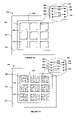
- FIG. 1 is an illustration of a reticle with test structures located within the scribe lines in accordance with one aspect of the present invention.
- FIG. 2 is an illustration of a reticle with test structures located in the device feature areas in accordance with another aspect of the present invention.
- FIG. 3 is an illustration of a reticle test system utilized to determine critical dimensions and/or defects in a reticle in accordance with an aspect of the present invention.
- FIG. 4 is an illustration of a test structure containing two adjacent lines, one open and one short, that may be utilized to create a digital signature in accordance with an aspect of the present invention.
- FIG. 5 is an illustration of a test structure containing four adjacent lines, two opens and two shorts, that may be utilized to create a digital signature and to determine critical dimensions and/or defects in a reticle in accordance with an aspect of the present invention.
- FIG. 6 is an illustration of a test structure containing a short with a defect which can be determined in accordance with an aspect of the present invention.
- FIG. 7 is an illustration of a test structure containing an open with a defect which can be determined in accordance with an aspect of the present invention.
- FIG. 8 is an illustration of a test structure containing metal lines which can be utilized to determine bridging defects between adjacent lines in accordance with an aspect of the present invention.
- FIG. 9 is an illustration of a test structure containing progressively longer metal line shorts which can be utilized to determine critical dimensions and/or defects in a reticle in accordance with an aspect of the present invention.
- FIG. 10 is an illustration of a test structure containing opens with progressively shorter discontinuities in the metal lines which can be utilized to determine critical dimensions and/or defects in a reticle in accordance with an aspect of the present invention.
- FIG. 11 is an illustration of a test structure containing progressively longer adjacent metal lines with 90 degree corners which can be utilized to determine critical dimensions and/or defects in a reticle in accordance with an aspect of the present invention.
- FIG. 12 is an illustration of a test structure containing progressively longer adjacent metal lines with multiple 90 degree corners which can be utilized to determine critical dimensions and/or defects in a reticle in accordance with an aspect of the present invention.
- FIG. 13 is an illustration of a test structure containing a variety of metal lines which can be utilized to determine critical dimensions and/or defects in a reticle in accordance with an aspect of the present invention.
- FIG. 14 is an illustration of a test structure containing four adjacent lines, two opens and two shorts, that may be utilized to create a digital signature and to determine critical dimensions and/or defects in a reticle in accordance with an aspect of the present invention.
- FIG. 15 is an illustration of a reticle with test structures located within the actual device feature areas in accordance with an aspect of the present invention.
- FIG. 16 is an illustration of a reticle with a plurality of test structures located within the actual device feature areas in accordance with an aspect of the present invention.
- FIG. 17 is an illustration of a reticle where features within the actual device feature areas are utilized as test features to determine critical dimensions and/or defects in a reticle in accordance with an aspect of the present invention.
- FIG. 18 is a flow diagram illustrating a methodology for determining defects in a reticle in accordance with an aspect of the present invention.
- FIG. 19 is a flow diagram illustrating a methodology for determining critical dimensions in a reticle in accordance with an aspect of the present invention.
- FIG. 1 illustrates reticle 10 in accordance with one aspect of the present invention.
- a reticle is used during the photolithography process to expose a resist layer coated on a wafer corresponding to the pattern formed on the reticle.
- the reticle 10 includes a plurality of device feature areas 26 which are used to expose a plurality of individual die or chips on a wafer or substrate.
- the device feature area is the area of the reticle where the features of the integrated circuits are located.
- Each device feature area 26 contains an identical pattern to be transferred to the wafer.
- Reticle 10 is illustrated as a brightfield reticle where patterned features to be transferred are opaque features on a clear background.
- Reticle substrate 12 can be any number of types of transparent material such as silica glass, fused quartz, or any other material transparent to the radiation commonly used in semiconductor lithographic operations.
- Metal layer 28 can be a composite material of chromium and gold, chromium and another metal, a homogeneous metal such as gold or other similar metals, or a combination of metals. Metal is used frequently throughout this application, but it is to be understood that any suitable metal or combination of metals may be used.
- Vertical lines and horizontal lines separate the device feature areas 26 from each other and form vertical scribe lines 14 and horizontal scribe lines 16 wherein the individual chips on the wafer may be cut.
- One or more test structures 18 are formed in the area of the scribe lines according to one aspect of the invention.
- a test structure is a collection of one or more test features.
- Test features are metal lines with at least two probe points, one located at either end of the line, operable for making electrical contact.
- the metal lines of the test feature may be designed as a contiguous line from one end to the other end (i.e., a short circuit, or short) or with a discontinuity between one end and the other end (i.e., an open circuit, or open).
- test features of various lengths and widths can be used to replicate the critical dimensions of the device feature areas.
- the test structures may be located in the scribe lines when the device feature areas 26 are too dense to allow for test structures to be formed within the device feature areas.
- Test structure 18 contains a series of metal lines 20 of increasing length.
- test structures in the vertical scribe lines contain vertical metal lines and test structures in the horizontal scribe lines contain horizontal metal lines.
- Each metal line 20 within a test structure 18 contains a first probe point 22 and a second probe point 24 . The first and second probe points are used to allow electrical contact to be made with each metal line 20 . By applying an appropriate voltage to the probe points of each metal line, the resistance of each metal line can be calculated and used to determine critical dimensions.
- FIG. 2 illustrates another aspect of the invention wherein test structures 38 are incorporated into the device feature areas 46 of the reticle.
- reticle 30 has substrate 32 and metal layer 48 .
- Vertical scribe lines 34 and horizontal scribe lines 36 separate device feature areas 46 from each other.
- no test structure is located within the vertical scribe lines 34 or the horizontal scribe lines 36 .
- each device feature area 46 contains an identical set of two test structures 38 , one each in opposite corners; the upper left hand corner and the lower right hand corner of the device feature area 46 .
- Each test structure 38 contains two metal lines of different lengths.
- Each metal line 40 within a test structure 38 contains a first probe point 42 and a second probe point 44 . The first and second probe points are used to allow electrical contact to be made with each metal line 40 . By applying an appropriate voltage to the probe points of each metal line, the resistance of each metal line can be calculated and used to determine critical dimensions.
- FIG. 3 is a schematic illustration of a reticle test system 50 for carrying out an aspect of the present invention.
- a reticle 52 is mounted on a carrier fixture 54 . Attached to the carrier is a spindle 56 .
- a carrier positioning system 58 is operative coupled to the spindle 56 .
- the carrier positioning system provides rotational and translational motion to the carrier allowing the reticle to be properly positioned below test head 60 .
- the test head contains one or more probes 61 which are utilized to probe the probe points on the test features within the test structures or device feature areas of the reticle.
- the test head 60 applies a voltage to the probes 61 , which in turn apply a voltage to the probe points of the test feature.
- a measurement system 62 checks the electrical continuity between appropriate probe points of the reticle and can determine the digital signature of the area under test. Electrical continuity exists when a complete path for current exists. By evaluating the response at various probe points to an applied voltage, defects in the reticle can be detected as described herein. The measurement system 62 can also measure the resultant current from a known applied voltage. From this information, the resistance of the test feature under test is determined. This resistance data is then used to determine the critical dimensions of the test feature under test.
- the system 50 includes a control system 64 and a display system 70 .
- the control system contains a processor 66 and a memory 68 .
- the processor 66 may be any one of a plurality of processors suitable for carrying out the present invention.
- the processor is operatively coupled to the memory system 68 , the measurement system 62 , a load system 72 , and the carrier positioning system 58 .
- the processor 66 receives the output of the measurement system 62 and compares the results to the expected results stored in memory 68 .
- the processor also determines the appropriate time and position that the reticle should be placed under the test head and provides an appropriate input to the positioning system.
- the positioning system moves the reticle at appropriate times to allow for additional measurements to be completed.
- the memory 68 stores expected results data which is supplied to the processor 66 .
- the memory 68 also serves to store program code which is executed by the processor 66 for carrying out the functions of the system.
- the memory also serves as a storage medium for temporarily storing information such as applied voltage, current measurements, resistance, carrier location, active probe points, and other data which may be necessary for carrying out the invention.
- An optional load system 72 provides the ability to rapidly load and unload a plurality of reticles onto the carrier in succession. As testing is completed on one reticle, the load system removes that reticle and loads the next one in succession for test.
- FIGS. 4–14 illustrate how open circuits and short circuits are employed according to another aspect of the invention.
- a short is a short circuit which is implemented as a contiguous conductive line segment with probe points located at each end of the conductive line.
- An open is an open circuit which is implemented as a conductive line segment with a discontinuity located between the probe points which are located at each end of the conductive line.
- a discontinuity is a break in a conductive line segment that interrupts the contiguous nature of the line. A discontinuity causes an incomplete path for current to exist.
- FIG. 4 illustrates a test structure 100 which contains an open 102 , and a short 104 .
- a short circuit is used to represent a digital 1, (“1”) and an open circuit is used to represent a digital 0, (“0”).
- FIG. 5 illustrates how opens and shorts can be used to create a test structure that defines a digital bit pattern of “1001”.
- Test structure 108 contains short 110 , open 112 , second open 114 , and second short 116 .
- probe points 118 and 120 are probed and the short circuit is detected and properly interpreted as a digital “1”.
- the reticle test system probes the probe points 122 and 124 , an open circuit is detected and properly interpreted as a digital “0”.
- line 114 is interpreted as a “0”
- line 116 is interpreted as a “1”. Therefore, the proper digital representation of the test structure in FIG. 5 is “1001”.
- Such digital representations are referred to as the digital signature of the test structure.
- the reticle test system can be used to probe a test structure and rapidly examine its digital signature. If a short circuit has a defect which breaks the contiguous nature of the line, then it is interpreted as a “0” instead of a “1”. This is illustrated in FIG. 6 .
- both line 130 and line 136 are designed to be short circuits which, if properly formed, are interpreted as “0”s by the reticle test system.
- a short circuit or “1” is properly determined for line 130 .
- line 136 contains a defect which breaks the line 136 near probe point 138 . This can be caused from a processing problem known as foreshortening of the line.
- the fact that a defect has occurred is determined when the reticle test system tests for electrical continuity between probe points 138 and 140 . In this case the reticle test system detects a “0” when it is expecting to detect a “1”. In this manner, the foreshortening defect is detected.
- a test feature may be purposely designed as a short like line 136 where the discontinuity is positioned in close proximity to probe point 138 .
- close proximity positioning is about 0.1 microns or more and about 10 microns or less.
- the close proximity positioning is about 0.2 microns or more and about 5 microns or less.
- a test feature such as line 136 may be used to verify that the line does not extend in length in such a manner as to complete a connection to probe point 138 . In this case the reticle test system detects a “1” when it is expecting to detect a “0”.
- both lines 144 and 150 are designed to be open circuits which, if properly formed, are interpreted as “0”s by the reticle test system.
- an open, or “0” is properly determined for line 144 .
- line 150 has a defect in it in which metal bridges the area intended to be open.
- a short, or “1” is determined for line 150 . In this manner, a defect that bridges the two halves of an open is detected.
- FIG. 8 illustrates yet another test structure in accordance with an aspect of the invention.
- the test structure in FIG. 8 can be utilized to look for bridging between closely spaced lines.
- Lines 160 and 166 are spaced to be representative of the closest line spacing utilized on the reticle. In one embodiment, the spacing is about 0.1 microns, or more and about 10 microns or less. In another embodiment, the spacing is about 0.2 microns, or more and about 5 microns or less.
- Lines 172 and 178 are similarly placed.
- a reticle test system which tests for electrical continuity between probe points 162 and 164 properly determines a “1” and between probe points 168 and 170 properly determines a “0”.
- a reticle test system now properly measures electrical continuity between probe points 174 and 176 and interprets a “1”. However, when electrical continuity is checked between probe points 180 and 182 , unexpected electrical continuity is detected and interpreted as a “1” instead of a “0”.
- the reticle test system can also be configured to detect the unexpected electrical continuity that exists between probe point 180 to probe points 174 and 176 and between probe point 182 to probe points 174 and 176 .
- the reticle test system detects the presence of the bridging while testing line 172 as electrical continuity is detected at probe points 180 and 182 while testing between probe points 174 and 176 . It should be understood that this same arrangement detects the bridging in a similar fashion even if the bridging exists in only one of the two locations illustrated. Therefore, this type of test structure is utilized to check for bridging between closely spaced lines.
- FIGS. 9–13 illustrate a few additional test structures that can be employed to test for various defects and/or critical dimensions.
- FIG. 9 illustrates a test structure 190 which contains a series of shorts of increasing length. Based on the actual device features, line 192 is representative of a line of minimum length; line 194 is representative of an average length line; and line 196 is representative of a line of maximum length.
- the reticle test system can be used to probe the probe points and determine a test structure signature or pattern of “111”. The reticle test system can determine whether any opens exists between the lines or whether any bridging exists between the individual lines. Additionally, since the applied voltage is know, by measuring the resultant current, the resistance of each line can be calculated. From the resulting resistance values, the critical dimensions of the lines are individually determined.
- FIG. 10 illustrates test structure 200 which contains a series of opens in which the size of the opening in the line is progressively smaller.
- the opening in line 204 is reduced by about 50% or more from the opening in line 202 .
- the opening in line 206 is reduced by about 50% or more from the opening in line 204 .
- This test structure can be used evaluate the ability to produce opens of various lengths. A reticle test system properly interprets this test structure signature as “000”. The reticle test system determines whether any bridging exists between the respective halves of each line or between the individual lines.
- FIG. 11 illustrates test structure 210 which contains a series of “L” shaped lines.
- Four progressively longer lines 212 , 214 , 216 , and 218 are evenly spaced at an interval representative of the line spacing employed in the device feature area of a reticle.
- This test structure is used to look for defects in closely spaced lines containing 90 degree corners. Rounding of the corners on 90 degree corners can sometimes result in opens.
- This structure has a test signature of “1111” since all lines are shorts. Again, a reticle test system determines whether an open exists or whether any bridging exists between lines. Additionally, since the applied voltage is know, by measuring the resultant current, the resistance of each line can be calculated. From the resulting resistance values, the critical dimensions of the metal lines are individually determined.
- metal lines 232 , 234 , 236 and 238 in test structure 230 each contain two 90 degree turns in opposite directions.
- This test structure can also be used to look for defects in closely spaced 90 degree turns in metal lines. Rounding of the corners on 90 degree turns can sometimes result in opens.
- This structure has a test signature of “1111” since all lines are shorts. Again, a reticle test system determines whether an open exists or whether any bridging exists between lines. Additionally, since the applied voltage is know, by measuring the resultant current, the resistance of each line can be calculated. From the resulting resistance values, the critical dimensions of the metal lines are individually determined.
- FIG. 13 illustrates a test structure in which a variety metal line sizes, shapes, spacing, opens and shorts are employed.
- a structure such as this is utilized to test for a variety of different defects and/or critical dimensions. It is to be understood that a test structure can be created containing any number of sizes, shapes and spacing so as to test for a variety of defects that are likely to occur in the device feature areas.
- This structure contains a straight metal line 252 , metal lines with 90 degree corners 254 , 256 and 258 , a line with 90 degree turns in opposite directions 260 , and opens 262 and 264 of different lengths.
- the applied voltage is known and by measuring the resultant current, the resistance of each line can be calculated. From the resulting resistance values, the critical dimensions of the metal lines are individually determined.
- test structure 270 is shown in FIG. 14 .
- test structure 270 four test features, a short 272 , an open 274 , a second open 276 , and a second short 278 , are employed.
- Short 272 has probe points 282 and 292 ;
- open 274 has probe points 284 and 294 ;
- open 276 has probe points 286 and 296 ;
- short 278 has probe points 288 and 298 .
- a reticle test system which measures electrical continuity at the probe points interprets a proper test structure as having a “1001” signature. This test structure is utilized to check for various defects. Additionally, since the applied voltage is know, by measuring the resultant current, the resistance of each line can be calculated. From the resulting resistance values, the critical dimensions of the metal lines are individually determined.
- FIG. 15 illustrates another aspect of the invention wherein test structures 270 are incorporated into the device feature areas 360 for the semiconductor chips.
- the contents of test structure 270 is identical to that described in FIG. 14 .
- reticle 350 has substrate 352 and metal layer 362 .
- Vertical scribe line 354 and horizontal scribe lines 356 separate device feature areas 360 from each other.
- no test structure is located within the vertical scribe lines 354 or the horizontal scribe lines 356 .
- each device feature area 360 contains an identical test structure 270 .
- the applied voltage is known. By measuring the resultant current, the resistance of each line can be calculated. From the resulting resistance values, the critical dimensions of the metal lines are individually determined.
- FIG. 16 illustrates a plurality of test structures 270 scattered through out the device feature areas 380 in accordance with one aspect of the invention.
- the contents of test structure 270 is identical to that described in FIG. 14 .
- reticle 370 has substrate 372 and metal layer 382 .
- Vertical scribe line 374 and horizontal scribe lines 376 separate device feature areas 380 from each other.
- no test structure is located within the vertical scribe lines 374 or the horizontal scribe lines 376 .
- each device feature area 380 contains a plurality of test structures 270 scattered throughout space available in the device feature areas 380 . Through use of the reticle test system, the applied voltage is known.
- each test structure is the same. However, it is to be understood that a variety of different test structures may be used depending on the space available at any given location within the device feature areas. Each test structure could, in fact, be different and could be designed to test for different defects.
- FIG. 17 illustrates yet another aspect of the invention.
- probe points may be included on one or more metal lines that form the integrated circuit features within the device feature areas of the reticle.
- the metal lines of the device area function as test features from which the reticle critical dimensions are directly evaluated. Certain defects can also be detected.
- reticle 400 has substrate 410 and metal layer 420 .
- Vertical scribe lines 430 and horizontal scribe lines 440 separate device feature areas 450 from each other.
- identical metal lines 460 exist within each device feature area 450 .
- 470 is an enlargement of a typical metal line 472 that forms a part of one of the identical device feature areas 450 .
- metal line 472 is fabricated with probe points 474 and 476 as part of the device feature area.
- Metal line 472 functions as a test feature. Accordingly, a reticle test system may be employed to check for defects and/or to evaluate the critical dimensions of the reticle at or near metal line 472 .
- probe points may be employed on one or more of the metal lines within the device feature area. Furthermore, the probe points may be included as part of one or more metal lines within one or more device feature areas within the reticle.
- FIG. 18 is a flow diagram illustrating a methodology 1800 for checking for defects in a reticle in accordance with the present invention.
- the methodology 1800 begins at 1810 where a complete reticle is loaded by the load system into the reticle carrier. The positioning system then properly positions the reticle so that the test head is engaged at 1820 .
- voltage is applied by the test head to a probe point of the reticle.
- the probe point may be one of the probe points of a test feature within a test structure of the reticle or one of the probe points of a test feature with the device feature areas of the reticle.
- the test head checks for electrical continuity responses at all other probe points within the reticle.
- determination is made as to whether the last probe point has been evaluated. If not, the process returns to 1830 to apply a voltage to the next probe point, otherwise the process proceeds to 1850 .
- the processor analyzes the applied voltages and recorded electrical continuity responses.
- determination is made on whether a defect exists. If a defect does exist, then at 1870 the information as to the type of defect and the location of the defect can be stored in memory and/or fed forward or backward for use in the reticle fabrication process of the current or subsequent reticles.
- the defective reticle is identified to be discarded, then the test head is disengaged at 1880 .
- the test head is disengaged at 1880 .
- the reticle is unloaded and at 1886 , determination is made as to whether the last reticle has been tested. If the last reticle has been tested, then the process is done at 1890 , if not, the process returns to 1810 to load a new reticle and the process continues until the last reticle has been tested.
- FIG. 19 is a flow diagram illustrating a methodology that may be employed for measuring critical dimensions of a reticle in accordance with the present invention.
- the methodology 1900 begins at 1910 where a complete reticle is loaded by the load system into the reticle carrier. The positioning system then properly positions the reticle so that the test head may be engaged at 1920 .
- a voltage is applied by the test head to the probe points of the reticle.
- the probe points may be the probe points of a test feature within a test structure of the reticle, or probe points on test features within the device feature area of the reticle, or both.
- the test head measures the current in responses to the voltage applied to the various probe points.
- the processor analyzes the applied voltages and resulting currents and determines the resistance values and critical dimensions of each feature tested.
- determination is made as to whether the critical dimensions are within the desired limits. If the critical dimensions are not within the desired limits, then at 1970 the information can be stored in memory and/or fed forward or backward for use in the fabrication process of the current or subsequent reticles.
- the defective reticle is identified to be discarded, then the test head is disengaged at 1980 .
- the test head is disengaged at 1980 .
- the reticle is unloaded and at 1986 , determination is made as to whether the last reticle has been tested. If the last reticle has been tested, then the process is done at 1990 , if not, the process returns to 1910 to load a new reticle and the process continues until the last reticle has been tested.
- FIG. 18 and FIG. 19 are merely illustrative of numerous methodologies that could be used to employ the present invention. It should also be understood that the two methods may be used in conjunction with each other to simultaneously look for defects and determine the critical dimensions of the reticle.
Abstract
Description
Claims (25)
Priority Applications (1)
| Application Number | Priority Date | Filing Date | Title |
|---|---|---|---|
| US10/160,334 US6972576B1 (en) | 2002-05-31 | 2002-05-31 | Electrical critical dimension measurement and defect detection for reticle fabrication |
Applications Claiming Priority (1)
| Application Number | Priority Date | Filing Date | Title |
|---|---|---|---|
| US10/160,334 US6972576B1 (en) | 2002-05-31 | 2002-05-31 | Electrical critical dimension measurement and defect detection for reticle fabrication |
Publications (1)
| Publication Number | Publication Date |
|---|---|
| US6972576B1 true US6972576B1 (en) | 2005-12-06 |
Family
ID=35430437
Family Applications (1)
| Application Number | Title | Priority Date | Filing Date |
|---|---|---|---|
| US10/160,334 Expired - Fee Related US6972576B1 (en) | 2002-05-31 | 2002-05-31 | Electrical critical dimension measurement and defect detection for reticle fabrication |
Country Status (1)
| Country | Link |
|---|---|
| US (1) | US6972576B1 (en) |
Cited By (11)
| Publication number | Priority date | Publication date | Assignee | Title |
|---|---|---|---|---|
| US7282374B1 (en) * | 2004-11-03 | 2007-10-16 | Advanced Micro Devices, Inc. | Method and apparatus for comparing device and non-device structures |
| US20070290694A1 (en) * | 2004-10-28 | 2007-12-20 | Mr. Arley Cleveland | System and apparatus for electrically testing lead-to-lead shorting during magnetoresistive sensor fabrication |
| US20080074130A1 (en) * | 2006-09-27 | 2008-03-27 | Taiwan Semiconductor Manufacturing Co., Ltd. | Apparatus and method for testing conductive bumps |
| US20080107329A1 (en) * | 2006-11-06 | 2008-05-08 | Jong-An Kim | Method of detecting defects of patterns on a semiconductor substrate and apparatus for performing the same |
| WO2008052940A2 (en) * | 2006-10-30 | 2008-05-08 | Koninklijke Philips Electronics N.V. | Test structure for detection of defect devices with lowered resistance |
| US7491476B1 (en) * | 2008-04-16 | 2009-02-17 | International Business Machines Corporation | Photomask electrical monitor for production photomasks |
| US20090148782A1 (en) * | 2007-12-10 | 2009-06-11 | Takuya Kono | Exposure method, photo mask, and reticle stage |
| CN101964377A (en) * | 2009-07-22 | 2011-02-02 | 日本麦可罗尼克斯股份有限公司 | Thin film characteristic measuring apparatus and method and thin film processing apparatus and method |
| WO2015148204A1 (en) * | 2014-03-26 | 2015-10-01 | Teradyne, Inc. | Current regulation for accurate and low-cost voltage measurements at the wafer level |
| US20150294918A1 (en) * | 2014-04-11 | 2015-10-15 | Global Foundries Us Inc. | Staggered electrical frame structures for frame area reduction |
| US11041900B2 (en) | 2014-03-26 | 2021-06-22 | Teradyne, Inc. | Equi-resistant probe distribution for high-accuracy voltage measurements at the wafer level |
Citations (14)
| Publication number | Priority date | Publication date | Assignee | Title |
|---|---|---|---|---|
| US4809341A (en) | 1986-07-18 | 1989-02-28 | Fujitsu Limited | Test method and apparatus for a reticle or mask pattern used in semiconductor device fabrication |
| US4926489A (en) | 1983-03-11 | 1990-05-15 | Kla Instruments Corporation | Reticle inspection system |
| US4927692A (en) * | 1988-11-25 | 1990-05-22 | International Business Machines Corporation | Antistatic mask for use with electronic test apparatus |
| US5240796A (en) | 1991-07-09 | 1993-08-31 | Micron Technology, Inc. | Method of fabricating a chromeless phase shift reticle |
| US5390420A (en) * | 1994-02-18 | 1995-02-21 | Seagate Technology, Inc. | MR element-to-contact alignment test structure |
| US5438272A (en) * | 1994-05-09 | 1995-08-01 | International Business Machines Corporation | Voltage-stressing and testing of networks using moving probes |
| US5460908A (en) | 1991-08-02 | 1995-10-24 | Micron Technology, Inc. | Phase shifting retical fabrication method |
| US5789120A (en) | 1996-06-04 | 1998-08-04 | Samsung Electronics Co., Ltd. | Method for designing a reticle mask |
| US5849440A (en) | 1996-07-02 | 1998-12-15 | Motorola, Inc. | Process for producing and inspecting a lithographic reticle and fabricating semiconductor devices using same |
| US5936707A (en) | 1996-06-10 | 1999-08-10 | Sharp Laboratories Of America, Inc. | Multi-level reticle system and method for forming multi-level resist profiles |
| US6027859A (en) | 1997-12-17 | 2000-02-22 | Advanced Micro Devices, Inc. | Semiconductor substrate having extended scribe line test structure and method of fabrication thereof |
| US6136479A (en) | 1998-07-03 | 2000-10-24 | Mitsubishi Denki Kabushiki Kaisha | Method of forming photomask and pattern and method of forming a semiconductor device |
| US6183915B1 (en) | 1998-11-25 | 2001-02-06 | Micron Technology, Inc. | Method of forming a phase shifting reticle |
| US6537708B2 (en) * | 2001-01-31 | 2003-03-25 | Photronics, Inc. | Electrical critical dimension measurements on photomasks |
-
2002
- 2002-05-31 US US10/160,334 patent/US6972576B1/en not_active Expired - Fee Related
Patent Citations (14)
| Publication number | Priority date | Publication date | Assignee | Title |
|---|---|---|---|---|
| US4926489A (en) | 1983-03-11 | 1990-05-15 | Kla Instruments Corporation | Reticle inspection system |
| US4809341A (en) | 1986-07-18 | 1989-02-28 | Fujitsu Limited | Test method and apparatus for a reticle or mask pattern used in semiconductor device fabrication |
| US4927692A (en) * | 1988-11-25 | 1990-05-22 | International Business Machines Corporation | Antistatic mask for use with electronic test apparatus |
| US5240796A (en) | 1991-07-09 | 1993-08-31 | Micron Technology, Inc. | Method of fabricating a chromeless phase shift reticle |
| US5460908A (en) | 1991-08-02 | 1995-10-24 | Micron Technology, Inc. | Phase shifting retical fabrication method |
| US5390420A (en) * | 1994-02-18 | 1995-02-21 | Seagate Technology, Inc. | MR element-to-contact alignment test structure |
| US5438272A (en) * | 1994-05-09 | 1995-08-01 | International Business Machines Corporation | Voltage-stressing and testing of networks using moving probes |
| US5789120A (en) | 1996-06-04 | 1998-08-04 | Samsung Electronics Co., Ltd. | Method for designing a reticle mask |
| US5936707A (en) | 1996-06-10 | 1999-08-10 | Sharp Laboratories Of America, Inc. | Multi-level reticle system and method for forming multi-level resist profiles |
| US5849440A (en) | 1996-07-02 | 1998-12-15 | Motorola, Inc. | Process for producing and inspecting a lithographic reticle and fabricating semiconductor devices using same |
| US6027859A (en) | 1997-12-17 | 2000-02-22 | Advanced Micro Devices, Inc. | Semiconductor substrate having extended scribe line test structure and method of fabrication thereof |
| US6136479A (en) | 1998-07-03 | 2000-10-24 | Mitsubishi Denki Kabushiki Kaisha | Method of forming photomask and pattern and method of forming a semiconductor device |
| US6183915B1 (en) | 1998-11-25 | 2001-02-06 | Micron Technology, Inc. | Method of forming a phase shifting reticle |
| US6537708B2 (en) * | 2001-01-31 | 2003-03-25 | Photronics, Inc. | Electrical critical dimension measurements on photomasks |
Cited By (20)
| Publication number | Priority date | Publication date | Assignee | Title |
|---|---|---|---|---|
| US20070290694A1 (en) * | 2004-10-28 | 2007-12-20 | Mr. Arley Cleveland | System and apparatus for electrically testing lead-to-lead shorting during magnetoresistive sensor fabrication |
| US7737703B2 (en) * | 2004-10-28 | 2010-06-15 | Hitachi Global Storage Technologies Netherlands B.V. | System and apparatus for electrically testing lead-to-lead shorting during magnetoresistive sensor fabrication |
| US7282374B1 (en) * | 2004-11-03 | 2007-10-16 | Advanced Micro Devices, Inc. | Method and apparatus for comparing device and non-device structures |
| US20080074130A1 (en) * | 2006-09-27 | 2008-03-27 | Taiwan Semiconductor Manufacturing Co., Ltd. | Apparatus and method for testing conductive bumps |
| US7439751B2 (en) * | 2006-09-27 | 2008-10-21 | Taiwan Semiconductor Manufacturing Co, Ltd. | Apparatus and method for testing conductive bumps |
| WO2008052940A3 (en) * | 2006-10-30 | 2008-07-03 | Koninkl Philips Electronics Nv | Test structure for detection of defect devices with lowered resistance |
| US20100060292A1 (en) * | 2006-10-30 | 2010-03-11 | Nxp, B.V. | Test structure for detection of defect devices with lowered resistance |
| US8264235B2 (en) * | 2006-10-30 | 2012-09-11 | Nxp B.V. | Test structure for detection of defect devices with lowered resistance |
| WO2008052940A2 (en) * | 2006-10-30 | 2008-05-08 | Koninklijke Philips Electronics N.V. | Test structure for detection of defect devices with lowered resistance |
| US8055056B2 (en) * | 2006-11-06 | 2011-11-08 | Samsung Electronics Co., Ltd. | Method of detecting defects of patterns on a semiconductor substrate and apparatus for performing the same |
| US20080107329A1 (en) * | 2006-11-06 | 2008-05-08 | Jong-An Kim | Method of detecting defects of patterns on a semiconductor substrate and apparatus for performing the same |
| US20090148782A1 (en) * | 2007-12-10 | 2009-06-11 | Takuya Kono | Exposure method, photo mask, and reticle stage |
| US7491476B1 (en) * | 2008-04-16 | 2009-02-17 | International Business Machines Corporation | Photomask electrical monitor for production photomasks |
| CN101964377A (en) * | 2009-07-22 | 2011-02-02 | 日本麦可罗尼克斯股份有限公司 | Thin film characteristic measuring apparatus and method and thin film processing apparatus and method |
| CN101964377B (en) * | 2009-07-22 | 2013-05-08 | 日本麦可罗尼克斯股份有限公司 | Thin film characteristic measuring apparatus and method and thin film processing apparatus and method |
| WO2015148204A1 (en) * | 2014-03-26 | 2015-10-01 | Teradyne, Inc. | Current regulation for accurate and low-cost voltage measurements at the wafer level |
| US10698020B2 (en) | 2014-03-26 | 2020-06-30 | Teradyne, Inc. | Current regulation for accurate and low-cost voltage measurements at the wafer level |
| US11041900B2 (en) | 2014-03-26 | 2021-06-22 | Teradyne, Inc. | Equi-resistant probe distribution for high-accuracy voltage measurements at the wafer level |
| US20150294918A1 (en) * | 2014-04-11 | 2015-10-15 | Global Foundries Us Inc. | Staggered electrical frame structures for frame area reduction |
| US9508618B2 (en) * | 2014-04-11 | 2016-11-29 | Globalfoundries Inc. | Staggered electrical frame structures for frame area reduction |
Similar Documents
| Publication | Publication Date | Title |
|---|---|---|
| US11348222B2 (en) | Methods and systems for inspection of wafers and reticles using designer intent data | |
| US7135344B2 (en) | Design-based monitoring | |
| US6784446B1 (en) | Reticle defect printability verification by resist latent image comparison | |
| JP4637114B2 (en) | How to simulate reticle layout data, inspect reticle layout data, and generate an inspection process for reticle layout data | |
| US6691052B1 (en) | Apparatus and methods for generating an inspection reference pattern | |
| US6972576B1 (en) | Electrical critical dimension measurement and defect detection for reticle fabrication | |
| KR0172801B1 (en) | Photomask of testing for processing margine and testing method | |
| US6562639B1 (en) | Utilizing electrical performance data to predict CD variations across stepper field | |
| US6546125B1 (en) | Photolithography monitoring using a golden image | |
| US7243331B2 (en) | Method and system for controlling the quality of a reticle | |
| KR20040084710A (en) | Substrate inspection system, substrate inspection method and substrate inspection apparatus | |
| JP4503924B2 (en) | Lithographic method and apparatus for forming semiconductor devices on a wafer | |
| US20220196580A1 (en) | Defect inspection methods of semiconductor wafers | |
| US7127359B2 (en) | Real-time mathematical model for wafer spin defect detection and for misalignment analyses | |
| US7856138B2 (en) | System, method and computer software product for inspecting charged particle responsive resist | |
| JPS58196445A (en) | Method of inspecting mask | |
| US20080092088A1 (en) | Process monitoring system and method | |
| KR100755049B1 (en) | Analysis method of defect on photo mask | |
| Warrick et al. | Application of intentional defect arrays for assessing wafer inspection tool capabilities | |
| KR20010003507A (en) | Method for inspection a photomask |
Legal Events
| Date | Code | Title | Description |
|---|---|---|---|
| AS | Assignment |
Owner name: ADVANCED MICRO DEVICES, INC., CALIFORNIA Free format text: ASSIGNMENT OF ASSIGNORS INTEREST;ASSIGNORS:LYONS, CHRISTOPHER F.;TABERY, CYRUS E.;PHAN, KHOI A.;AND OTHERS;REEL/FRAME:012966/0813;SIGNING DATES FROM 20020513 TO 20020522 |
|
| AS | Assignment |
Owner name: ADVANCED MICRO DEVICES, INC., CALIFORNIA Free format text: CORRECTIVE DOCUMENT RE-RECORD TO CORRECT ERROR CONTAINED IN PROPERTY NUMBER 10034233 PREVIOUSLY RECORDED ON REEL 012966 FRAME 0813.;ASSIGNORS:LYONS, CHRISTOPHER F.;TABERY, CYRUS E.;PHAN, KHOI A.;AND OTHERS;REEL/FRAME:013097/0317;SIGNING DATES FROM 20020513 TO 20020522 |
|
| FPAY | Fee payment |
Year of fee payment: 4 |
|
| AS | Assignment |
Owner name: GLOBALFOUNDRIES INC., CAYMAN ISLANDS Free format text: AFFIRMATION OF PATENT ASSIGNMENT;ASSIGNOR:ADVANCED MICRO DEVICES, INC.;REEL/FRAME:023119/0083 Effective date: 20090630 |
|
| FPAY | Fee payment |
Year of fee payment: 8 |
|
| REMI | Maintenance fee reminder mailed | ||
| LAPS | Lapse for failure to pay maintenance fees |
Free format text: PATENT EXPIRED FOR FAILURE TO PAY MAINTENANCE FEES (ORIGINAL EVENT CODE: EXP.) |
|
| STCH | Information on status: patent discontinuation |
Free format text: PATENT EXPIRED DUE TO NONPAYMENT OF MAINTENANCE FEES UNDER 37 CFR 1.362 |
|
| FP | Lapsed due to failure to pay maintenance fee |
Effective date: 20171206 |
|
| AS | Assignment |
Owner name: GLOBALFOUNDRIES U.S. INC., NEW YORK Free format text: RELEASE BY SECURED PARTY;ASSIGNOR:WILMINGTON TRUST, NATIONAL ASSOCIATION;REEL/FRAME:056987/0001 Effective date: 20201117 |