US6959222B1 - Accelerator engine for processing functions used in audio algorithms - Google Patents
Accelerator engine for processing functions used in audio algorithms Download PDFInfo
- Publication number
- US6959222B1 US6959222B1 US09/548,849 US54884900A US6959222B1 US 6959222 B1 US6959222 B1 US 6959222B1 US 54884900 A US54884900 A US 54884900A US 6959222 B1 US6959222 B1 US 6959222B1
- Authority
- US
- United States
- Prior art keywords
- data
- accelerator engine
- chip
- engine
- dsp
- Prior art date
- Legal status (The legal status is an assumption and is not a legal conclusion. Google has not performed a legal analysis and makes no representation as to the accuracy of the status listed.)
- Expired - Fee Related
Links
Images


Classifications
-
- G—PHYSICS
- G06—COMPUTING; CALCULATING OR COUNTING
- G06F—ELECTRIC DIGITAL DATA PROCESSING
- G06F17/00—Digital computing or data processing equipment or methods, specially adapted for specific functions
- G06F17/10—Complex mathematical operations
- G06F17/14—Fourier, Walsh or analogous domain transformations, e.g. Laplace, Hilbert, Karhunen-Loeve, transforms
- G06F17/141—Discrete Fourier transforms
- G06F17/142—Fast Fourier transforms, e.g. using a Cooley-Tukey type algorithm
Definitions
- This invention relates generally to audio digital signal processing (DSP) and more particularly to processing functions used in audio algorithms.
- IDCT Inverse Discrete Cosine Transformation
- IFFT inverse Fast Fourier Transformation
- post-multiplication IDCT is used as one of the last stages of the Dolby®'s third generation audio coding (AC3) decompressing process.
- a subscript r denotes the real part
- a subscript i denotes the imaginary part of the complex number.
- FIG. 1 shows an audio integrated circuit chip 100 that includes a DSP 102 , a Random Access Memory (RAM) 106 , a Read Only Memory (ROM) 110 , and an Input/Output (I/O) interface 114 .
- DSP 102 provides the main digital signal processing for chip 100 including, for example, filtering and transforming audio samples.
- RAM 106 is a “memory on chip” used by programs running on DSP 102 to store data relating to input audio samples and the processing performed on those samples.
- ROM 110 stores additional data for DSP 102 .
- I/O interface 114 implements various protocols for exchanging, via databus 4005 , audio samples with external devices such as analog-to-digital (A/D) and digital-to-analog (D/A) converters, etc.
- A/D analog-to-digital
- D/A digital-to-analog
- DSP 102 cannot perform as fast as desired, that is, it cannot execute as many million instructions per second (MIPs) as are required to do all of the tasks demanded by chip 100 , including, for example, receiving AC3 data, detecting AC3 data error, using IDCT to decode data, and performing audio enhancement and 3D features.
- MIPs million instructions per second
- One approach to improving DSP 102 performance, or to conserving DSP 102 MIPs for other desired functions accelerates the AC3 decompressing stage. However, this approach requires operations that are tightly coupled with the AC3 algorithm, which in turn requires that a designer be intimately familiar with the AC3 decoding process. Further, the approach is useful for accelerating AC3, but provides no benefits for other audio functions or Moving Picture Expert Group (MPEG) functions.
- MPEG Moving Picture Expert Group
- the present invention provides an accelerator engine running in parallel with a DSP in an audio chip to improve its performance.
- the engine avoids AC3-specific algorithms and focuses on general purpose DSP functions, including biquad filtering and IDCT, that comprise pre-multiplication, IFFT, and post-multiplication.
- the DSP is therefore free to do other processing while the engine is performing a requested function.
- the engine utilizes its resources in a pipeline structure for increased efficiency. In the biquad and double precision biquad modes the engine stores data in predefined locations in memory to efficiently access the data.
- the engine also uses an equation and data values stored in the predefined locations to calculate an audio sample. The calculated result is then stored in a memory location in a way that it can easily be used to calculate the next sample.
- the engine efficiently saves 15 MIPs in an AC3 based 3D audio product, including 7.5 MIPs in the AC3 decoding process by accelerating the IFFT, and 7.5 MIPs from the 3D processing via a biquad filtering function.
- FIG. 1 shows a prior art DSP chip
- FIG. 2 shows a chip utilizing the accelerator engine according to the invention
- FIG. 3 is a block diagram of the accelerator engine
- FIG. 4A shows a pipeline structure for the pre-multiplication mode
- FIG. 4B shows a resource utilization map for the pre-multiplication mode
- FIG. 5A shows a pipeline structure for the FFT mode
- FIG. 5B shows a resource utilization map for the FFT mode
- FIG. 5C shows C code describing the address generation for both 128-point and 64-point FFTs
- FIG. 6A shows a pipeline structure for the biquad filtering mode
- FIG. 6B shows a resource utilization map for the biquad filtering mode
- FIG. 6C is a flowchart illustrating how the accelerator engine processes the biquad filtering
- FIG. 6D is a flowchart illustrating how the accelerator engine stores data during the biquad filtering mode
- FIG. 6E illustrates data in memory during a biquad filtering mode
- FIG. 7A shows a pipeline structure for the double precision biquad filtering mode
- FIG. 7B shows a resource utilization map for the double precision biquad filtering mode:
- FIG. 7C illustrates data in memory during a double precision biquad filtering mode
- FIG. 8 is a flowchart illustrating how a chip requests that a function be performed by the accelerator engine.
- the present invention provides an accelerator engine running in parallel with a DSP for processing functions that are usable by audio algorithms including, for example, AC3, 3D, bass managements, MP3, etc., and that would otherwise be performed by the DSP. Consequently, the DSP is free to process other tasks.
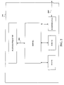
- FIG. 2 shows a chip 250 utilizing the invention.
- Integrated circuit chip 250 is like chip 100 except that chip 250 includes an accelerator engine 200 interfacing via data bus 2003 with DSP 102 .
- Data passing through databus 2003 includes configuration information and data for accelerator engine 200 to perform a requested function.
- FIG. 3 is a block diagram of accelerator engine 200 preferably including an RRAM 304 , an IRAM 308 , a ROM 312 , a control register 316 , a state machine 320 , a multiplier (MPY) 326 , a shift/sign extender 328 , an ALU 330 , and other components.
- accelerator engine 200 supports the following functions: single biquad filtering; double precision biquad filtering; radix2, 7 passes, 128-point IFFT; radix2, 6 passes, 64-point IFFT, premultiplication 128-word and 64-word configurations, post-multiplication 128-word and 64-word configurations. IDCT 128-word and 64-word configurations, and BFE-RAM read/write.
- RRAM 304 depending on the required function, stores different types of values. For example, for a biquad filtering function, RRAM 304 stores filter coefficients. For IFFT and IDCT functions, RRAM 304 stores real parts and IRAM 308 stores imaginary parts of complex numbers required by these functions. Data in RRAM 304 and IRAM 308 , where appropriate, contains new values after each time accelerator engine 200 has calculated an audio sample.
- ROM 312 is used in IFFT and IDCT modes preferably to store both real and imaginary values for complex numbers required by IFFT and IDCT functions.
- State machine 320 generates addresses for RRAM 304 , IRAM 308 , and ROM 312 and control signals for other circuitry of accelerator engine 200 .
- MPY 326 is preferably a conventional 24-bit multiplier for multiplying data on lines 3031 and 3035 .
- Shifter/Sign-Extender 328 shifts its contents to adjust or mask a sign bit on lines 3041 and 3045 .
- ALU 330 is preferably a conventional ALU which accumules, adds, or subtracts data on lines 3051 and 3055 .
- ALU 330 can be divided into an ALUA (not shown) and an ALUB (not shown) for use when two ALUs are required, such as in the pre-multiplication, IFFT, and post-multiplication modes.
- Multiplexers (MUXes) M 01 , M 03 , M 05 , M 07 , M 09 , M 11 , and M 13 perform conventional functions of MUXes, that is, passing selected inputs based on select signals (not shown) provided by state machine 320 and appropriate circuitry.
- Latches L 01 , L 03 , L 05 , L 07 , L 08 , L 09 , L 11 , L 13 , L 15 , and L 17 perform conventional functions of latches including passing inputs based on clocking signals (not shown) provided by state machine 320 and appropriate circuitry.
- Each column represents a critical resource (RRAM 304 , IRAM 308 , MPY 326 , etc.).
- Each row represents a phase-one-to-phase-one clock cycle, which lasts 20 ns in a preferred embodiment.
- the tables show what each resource is doing during each cycle.
- the number in each entry represents the number of operations a resource is executing during a given cycle. A “0” indicates a resource is idle; a “1” indicates a resource is busy.
- Parameters a m and a in represent data in RRAM 304 and IRAM 308 , respectively, and C n are filter coefficients in ROM 312 .
- n ranges from 0 to 127 (for 128 data points).
- the pre- and post-multiplication modes are identical except that data is accessed linearly in the pre-multiplication mode and in bit-reverse order in the post-multiplication mode because the IFFT mode leaves its results in bit-reverse order. Coefficients are accessed linearly in both the pre- and the post-multiplication modes.
- FIG. 4A shows a pipeline structure for the pre-multiplication mode.
- accelerator engine 200 reads b r from RRAM 304 , b i from IRAM 308 , and c r from ROM 312 .
- cycle 2 accelerator engine 200 reads c i from ROM 312 .
- MPY 326 performs b r *c r , b i *c i , b r *c i , and b i *c r , respectively.
- Accelerator engine 200 instead of using the same c r and c i that were read from ROM 312 in cycles 1 and 2 , rereads c i and c r from ROM 312 in cycles 3 and 4 . Rereading these values in cycles 3 and 4 avoids using a register to store the values read in cycles 1 and 2 . Further, ROM 312 is available for accessing its data in cycles 3 and 4 .
- accelerator engine 200 writes b r and b i into RRAM 304 and IRAM 308 , respectively.
- data required for a function in each cycle is made available before the data is needed.
- b r and c r used by MPY 326 in cycle 3 have been made ready to MPY 326 by reading RRAM 304 and IRAM 308 in cycle 1 .
- FIG. 4B shows a resource utilization map for the pre-multiplication mode, which, starting on any four cycle boundary and taking four cycles, shows the number of operations a resource is executing.
- MPY 326 and ROM 312 perform four operations (all four 1's), one in each of the four selected cycles 1 to 4 .
- ALUA performs two operations (one in each of cycles 2 and 3 ) while ALUB performs two operations (one in each of cycles 1 and 4 ).
- Data is accessed in cycles 1 and 2 for RRAM 304 and IRAM 308 . Therefore, MPY 326 and ROM 312 are utilized 100% of the time (4 operations in tour cycles) while each of ALUA, ALUB, RRAM 304 , and IRAM 308 is utilized 50% of the time (2 operations in 4 cycles).
- FIG. 5A shows a pipeline structure for the IFFT mode
- FIG. 5B shows a resource utilization map for the IFFT mode.
- the explanations of this IFFT pipeline structure and resource utilization map are similar to the respective explanations of the pre-multiplication mode in FIGS. 4A and 4B .
- cycle 1 accelerator engine 200 reads b r and c r from RRAM 304 and ROM 312 respectively; MPY 326 is utilized 100% of the time because in the selected four cycles MPY 326 performs four operations; etc. Consequently, as shown in FIG. 5B , all resources are utilized 100% of the time.
- Accelerator engine 200 performs each pass of the IFFT mode sequentially in both 128-point IFFT and 64-point IFFT. The difference between each pass is the method by which data points are addressed. The addressing schemes for the two modes are similar.
- FIG. 5C lists C-code describing the address generation for both 128-point FFT and 64-point FFT modes.
- Accelerator engine 200 stores filter coefficients in RRAM 304 and input samples and filter states in IRAM 308 .
- 48-bit ALU 330 remains as one ALU (instead of being divided into two ALUs: ALUA and ALUB).
- FIG. 6A shows a pipeline structure for the biquad filtering mode.
- FIG. 6B shows a resource utilization map for the biquad filtering mode. This pipeline structure can be repeated every six cycles and all resources will be used five out of every six cycles.
- FIG. 6C is a flowchart illustrating a method for accelerator engine 200 to perform a biquad filtering in accordance with the invention.
- accelerator engine 200 receives, for example, 124 sample data points represented by x 0 to x 123 .
- accelerator engine 200 stores data in IRAM 308 .
- Accelerator engine 200 then continues to receive, store, and calculate sampled data in respective steps 604 , 608 , and 612 until all data has been received. Then accelerator engine 200 completes the biquad filtering function in step 620 .
- FIG. 6D is a flowchart illustrating how accelerator engine 200 , in accordance with steps 608 and 612 of FIG. 6C , calculates and stores y n in IRAM 308 locations for 124 samples of x n from x 0 to x 123 .
- accelerator engine 200 stores x 0 to x 123 in locations 4 to location 127 .
- Accelerator engine 200 also stores values of y ⁇ 2 , y ⁇ 1 , x ⁇ 2 , and x ⁇ 1 in locations 0 , 1 , 2 , and 3 , respectively.
- FIG. 6D is a flowchart illustrating how accelerator engine 200 , in accordance with steps 608 and 612 of FIG. 6C , calculates and stores y n in IRAM 308 locations for 124 samples of x n from x 0 to x 123 .
- step 604 D accelerator engine 200 stores x 0 to x 123 in locations 4 to location 127 .
- locations 0 to 127 are used for illustrative purpose only, any 128 locations, for example, 1 to 128, 2 to 129, or K to K+128 ⁇ 1 are applicable.
- accelerator engine 200 uses the values in locations 0 , 1 , 2 , 3 , and 4 to calculate y 0 .
- step 612 D accelerator engine 200 stores the value of y 0 in location 2 . Accelerator engine 200 then returns to step 608 D to calculate y 1 and store y 1 in location 3 , which is one location higher than location 2 storing y 0 .
- Accelerator engine 200 keeps calculating and storing values of y until accelerator engine 200 is done, that is, accelerator engine 200 calculates and stores values of y 2 to y 123 in location 4 through location 125 , respectively.
- Accelerator engine 200 in calculating y 0 to y 123 , uses values of a 2 , a 1 , b 2 , b 1 , and b 0 preferably stored in ROM 312 .
- the invention uses the zero value for each of y ⁇ 2 , y ⁇ 1 , x ⁇ 2 , and x ⁇ 1 , to calculate the first sequence of 124 x n samples.
- FIG. 6E illustrates how IRAM 308 stores a data value for each y n from y 0 to y 123 .
- the “Address” column shows locations from 0 to 127 in IRAM 308 .
- the “Initial Data” column shows data of y ⁇ 2 , y ⁇ 1 , x ⁇ 2 , x ⁇ 1 , and x 0 to x 123 in corresponding locations of the “Address” column.
- Box 655 includes values (of y ⁇ 2 , y ⁇ 1 , x ⁇ 2 , x ⁇ 1 , and x 0 ) that are used to calculate y 0 .
- boxes 659 , 663 , and 669 include values (y ⁇ 1 , y 0 , x ⁇ 1 , etc.) that are used to calculate y 1 , y 2 , and y 3 , respectively.
- IRAM 308 locations of values in boxes 655 , 659 , 663 and 669 , etc., are increased by one for each increment of n.
- box 655 includes values in locations 0 through 4
- box 659 includes values in locations 1 through 5
- box 663 includes values in locations 2 through 6
- box 669 includes values in locations 3 through 7
- Arrow 602 indicates that y 1 is stored in location three, which is one location higher than the location of y 0
- arrow 604 indicates that y 2 is stored in location four, one location higher than the location of y 1 .
- the invention thus uses the same IRAM 308 locations from location 0 to location 127 for calculating and storing y n for subsequent sequences of 124 samples of x.
- the invention uses the zero value for y ⁇ , y ⁇ 1 , x ⁇ 2 , and x ⁇ 1 for the first sequence of 124 samples of x.
- the invention uses y 122 , y 123 , x 122 , and x 123 for y ⁇ 2 , y ⁇ 1 , x ⁇ 2 , and x ⁇ 1 , respectively.
- the invention uses y 246 , y 247 , x 246 , and x 247 for y ⁇ 2 , y ⁇ 1 , x ⁇ 2 and x ⁇ 1 , respectively.
- accelerator engine 200 stores filter coefficients preferably in RRAM 304 in order of a 2 , a 1 , b 2 , b 1 , and b 0 .
- the double precision biquad mode is similar to the (single) biquad mode, but the feedback state is stored and calculated as double precision for greater numerical stability.
- a double precision term y n comprises 48 bits, and therefore each term y ln and yh n comprises 24 bits.
- FIG. 7A shows a pipeline structure for the double precision biquad mode.
- FIG. 7B shows a resource utilization map for the double precision biquad mode.
- accelerator engine 200 operates in a pipeline fashion that repeats every nine cycles.
- the method for calculating y n in the double precision mode is similar to that for calculating in the biquad mode except, instead of five values (x n , x n ⁇ 1 , x n ⁇ 2 , y n ⁇ 1 , and y n ⁇ 2 ) accelerator engine 200 uses seven values (x n , x n ⁇ 1 , x ⁇ 2 , yl n ⁇ 1 , yl n ⁇ 2 , yh n ⁇ 1 , and yh n ⁇ 2 ) as required by equation (2), to calculate each y n . Further, after calculating y 0 , the invention stores yh 0 and yl 0 in respective locations 2 and 4 .
- the invention stores yh 1 and yl 1 in respective locations 3 and 5 , each location being one higher than the respective locations of yh 0 and yl 0 .
- the invention stores yh n and yin each in one location higher than the locations of respective yh n ⁇ 1 and yl n ⁇ 1 .
- FIG. 7C shows how accelerator engine 200 stores calculating and calculated values in IRAM 308 for the double precision biquad mode.
- the “Address” column shows locations from 0 to 127 in IRAM 308 .
- the “Initial Data” column shows data of yh ⁇ 2 , yh ⁇ 1 , yl ⁇ 2 , yl ⁇ 1 , x ⁇ 2 , x ⁇ 1 , and x 0 to x 121 in corresponding locations of the “Address” column.
- Box 755 includes values (of yh ⁇ 2 , yh ⁇ 1 , yl ⁇ 2 , yl ⁇ 1 , x ⁇ 2 , x ⁇ 1 , and x 0 ) that are used to calculate y 0 .
- boxes 759 , 763 , and 769 include values (yh ⁇ 1 , yh 0 , yl ⁇ 1 , yl 0 , x ⁇ 1 , etc.) that are used to calculate y 1 , y 2 , and y 3 , respectively.
- IRAM 308 locations of values in boxes 759 , 763 , 769 , etc. are increased by one for each increment of n.
- box 755 includes values in locations 0 through 6
- box 759 includes values in locations 1 through 7
- box 763 includes values in locations 2 through 8
- box 769 includes values in locations 3 through 9
- Arrow 702 indicates that yh 1 is stored in location 3 , which is one location higher than the location of yh 0
- Arrow 703 indicates that yl 1 is stored in location 5 , which is one location higher than the location of yl 0
- arrows 704 and 705 indicate that yh 2 and yl 2 are each stored in locations one higher than the respective locations of yh 1 and yl 1 , etc.
- the invention thus uses the same IRAM 308 locations from location 0 to location 127 for calculating and storing y n for subsequent sequences of 122 samples of x.
- the invention uses the zero value for yh ⁇ 2 , yh ⁇ 1 , yl ⁇ 2 , yl ⁇ 1 , x ⁇ 2 , and x ⁇ 1 for the first sequence of 122 samples of x.
- the invention uses yh 120 , yh 121 , yl 120 , yl 121 , x 120 , and x 121 for yh ⁇ 2 , yh ⁇ 1 , yl ⁇ 2 , yl ⁇ 1 , x ⁇ 2 , and x ⁇ 1 , respectively.
- accelerator engine 200 stores filter coefficients preferably in RRAM 304 in order of a 2 , a 1 , a 2 , a 1 , b 2 , b 1 , b 0 .
- FIG. 8 is a flowchart illustrating how chip 100 invokes a function performed by accelerator engine 200 .
- chip 100 writes to configuration register 316 to set the required mode and halt accelerator engine 200 .
- chip 100 downloads required data from chip 100 to accelerator engine 200 .
- For the pre-multiplication. IFFT, or post-multiplication modes chip 100 downloads data preferably in the order of 0 to 127 and alternating between RRAM 304 and IRAM 308 .
- chip 100 downloads coefficients preferably in the order of a 2 , a 1 , b 2 , b 1 , and b 0 in RRAM 304 .
- chip 100 downloads coefficients preferably in the order of a 2 , a 1 , a 2 , a 1 , b 2 , b 1 , and b 0 .
- Chip 100 also downloads data in the order from 0 to 127, which is the order shown in the “Initial Data” column in FIG. 6E .
- chip 100 determines whether all of the data has been downloaded. If the data is not completely downloaded then chip 100 in step 808 keeps downloading data, but if data is completely downloaded then chip 100 in step 816 sets the run bit in configuration register 316 so that accelerator engine 200 in step 820 can perform the requested function.
- Chip 100 in step 824 monitors the status of the done bit in configuration register 316 to determine whether accelerator engine 200 has completed its requested task.
- accelerator engine 200 completes its requested task, and, depending on the mode, chip 100 may or may not set the done bit in configuration register 316 .
- chip 100 via bus 2003 ( FIG. 2 ), reads data from accelerator engine 200 in linear order except in the IFFT mode where IFFT functions leave data in bit-reverse order.
Landscapes
- Physics & Mathematics (AREA)
- Mathematical Physics (AREA)
- Engineering & Computer Science (AREA)
- General Physics & Mathematics (AREA)
- Computational Mathematics (AREA)
- Mathematical Analysis (AREA)
- Mathematical Optimization (AREA)
- Pure & Applied Mathematics (AREA)
- Data Mining & Analysis (AREA)
- Theoretical Computer Science (AREA)
- Discrete Mathematics (AREA)
- Algebra (AREA)
- Databases & Information Systems (AREA)
- Software Systems (AREA)
- General Engineering & Computer Science (AREA)
- Complex Calculations (AREA)
Abstract
Description
A′=A−BC and B′=A+BC,
where A, A′, B, B′ and C are complex numbers in the form of D=dr+jdi. A subscript r denotes the real part, and a subscript i denotes the imaginary part of the complex number.
A n =A n C n where
A n =a m +ja in and
C n =c m +jc in.
Parameters am and ain represent data in
A′=A−BC and B′=A+BC,
where A, A′, B, B′, and C are complex numbers.
y n =b 0 x n +b 1 x n−1 +b 2 x n−2 +a 1 y n−1 +a 2 y n−2 (1)
where the subscript n indicates the current sample number; xn is the current input sample and yn is the current output sample; and b0, b1, b2, a1, and a2 are filter coefficients.
y n =b 0 x n +b 1 x n−1 +b 2 x n−2 +a 1 yl n−1 +a 2 yl n−2 (2)
in which yln represents the lower half bits and yhn represents the upper half bits of yn. In the preferred embodiment, a double precision term yn comprises 48 bits, and therefore each term yln and yhn comprises 24 bits.
Claims (1)
Priority Applications (1)
| Application Number | Priority Date | Filing Date | Title |
|---|---|---|---|
| US09/548,849 US6959222B1 (en) | 2000-04-13 | 2000-04-13 | Accelerator engine for processing functions used in audio algorithms |
Applications Claiming Priority (1)
| Application Number | Priority Date | Filing Date | Title |
|---|---|---|---|
| US09/548,849 US6959222B1 (en) | 2000-04-13 | 2000-04-13 | Accelerator engine for processing functions used in audio algorithms |
Publications (1)
| Publication Number | Publication Date |
|---|---|
| US6959222B1 true US6959222B1 (en) | 2005-10-25 |
Family
ID=35115378
Family Applications (1)
| Application Number | Title | Priority Date | Filing Date |
|---|---|---|---|
| US09/548,849 Expired - Fee Related US6959222B1 (en) | 2000-04-13 | 2000-04-13 | Accelerator engine for processing functions used in audio algorithms |
Country Status (1)
| Country | Link |
|---|---|
| US (1) | US6959222B1 (en) |
Cited By (1)
| Publication number | Priority date | Publication date | Assignee | Title |
|---|---|---|---|---|
| CN110175017A (en) * | 2019-05-23 | 2019-08-27 | 浙江大学 | A kind of multiplier and its operating method based on RRAM |
Citations (5)
| Publication number | Priority date | Publication date | Assignee | Title |
|---|---|---|---|---|
| US5901301A (en) * | 1996-02-07 | 1999-05-04 | Mitsubishi Denki Kabushiki Kaisha | Data processor and method of processing data |
| US6253293B1 (en) * | 1997-11-14 | 2001-06-26 | Cirrus Logic, Inc. | Methods for processing audio information in a multiple processor audio decoder |
| US6311204B1 (en) * | 1996-10-11 | 2001-10-30 | C-Cube Semiconductor Ii Inc. | Processing system with register-based process sharing |
| US6405227B1 (en) * | 1998-12-31 | 2002-06-11 | New Japan Radio Co., Ltd. | Digital crossover and parametric equalizer |
| US6430529B1 (en) * | 1999-02-26 | 2002-08-06 | Sony Corporation | System and method for efficient time-domain aliasing cancellation |
-
2000
- 2000-04-13 US US09/548,849 patent/US6959222B1/en not_active Expired - Fee Related
Patent Citations (5)
| Publication number | Priority date | Publication date | Assignee | Title |
|---|---|---|---|---|
| US5901301A (en) * | 1996-02-07 | 1999-05-04 | Mitsubishi Denki Kabushiki Kaisha | Data processor and method of processing data |
| US6311204B1 (en) * | 1996-10-11 | 2001-10-30 | C-Cube Semiconductor Ii Inc. | Processing system with register-based process sharing |
| US6253293B1 (en) * | 1997-11-14 | 2001-06-26 | Cirrus Logic, Inc. | Methods for processing audio information in a multiple processor audio decoder |
| US6405227B1 (en) * | 1998-12-31 | 2002-06-11 | New Japan Radio Co., Ltd. | Digital crossover and parametric equalizer |
| US6430529B1 (en) * | 1999-02-26 | 2002-08-06 | Sony Corporation | System and method for efficient time-domain aliasing cancellation |
Cited By (2)
| Publication number | Priority date | Publication date | Assignee | Title |
|---|---|---|---|---|
| CN110175017A (en) * | 2019-05-23 | 2019-08-27 | 浙江大学 | A kind of multiplier and its operating method based on RRAM |
| CN110175017B (en) * | 2019-05-23 | 2021-07-02 | 浙江大学 | Multiplier based on RRAM and operation method thereof |
Similar Documents
| Publication | Publication Date | Title |
|---|---|---|
| AU753685B2 (en) | Pipelined fast fourier transform processor | |
| JP3749022B2 (en) | Parallel system with fast latency and array processing with short waiting time | |
| US7640284B1 (en) | Bit reversal methods for a parallel processor | |
| KR20060096511A (en) | Fft architecture and method | |
| JP3938238B2 (en) | Fast Fourier transform processor | |
| JPS58169675A (en) | Monolithic type high speed fourier transform circuit | |
| US6317770B1 (en) | High speed digital signal processor | |
| US6993547B2 (en) | Address generator for fast fourier transform processor | |
| KR20090127462A (en) | Fast fourier transform/inverse fast fourier transform operating core | |
| US6959222B1 (en) | Accelerator engine for processing functions used in audio algorithms | |
| JP2006313518A (en) | Multi-dimensional fast fourier transformation | |
| JP4083387B2 (en) | Compute discrete Fourier transform | |
| JP3709291B2 (en) | Fast complex Fourier transform method and apparatus | |
| US6976047B1 (en) | Skipped carry incrementer for FFT address generation | |
| CN112835073A (en) | FFT (fast Fourier transform) processor for satellite signal acquisition | |
| JP2002504250A (en) | Device for converting a sequence of data elements | |
| US7447722B2 (en) | Low latency computation in real time utilizing a DSP processor | |
| CN1320444C (en) | Data processing unit | |
| JP2002507305A (en) | Device for converting a sequence of data elements | |
| JP2002207718A (en) | Method for fft processing | |
| Jian et al. | A memory-based hardware accelerator for real-time MPEG-4 audio coding and reverberation | |
| JP2708013B2 (en) | Memory control circuit for N-point FFT processor | |
| JP2000067032A (en) | Device and method for high-speed improved discrete cosine transformation | |
| Vojir | The impact of advanced computational techniques on digital avionics signal processor performance | |
| Santin | A multi-purpose set of routines for the Fast Fourier Transform |
Legal Events
| Date | Code | Title | Description |
|---|---|---|---|
| AS | Assignment |
Owner name: NEW JAPAN RADIO CO., LTD., JAPAN Free format text: ASSIGNMENT OF ASSIGNORS INTEREST;ASSIGNORS:VUONG, KENT;PAN, MICHAEL;SEAGRAVES, ERNEST;REEL/FRAME:010739/0417;SIGNING DATES FROM 20000103 TO 20000407 |
|
| FPAY | Fee payment |
Year of fee payment: 4 |
|
| FPAY | Fee payment |
Year of fee payment: 8 |
|
| REMI | Maintenance fee reminder mailed | ||
| LAPS | Lapse for failure to pay maintenance fees |
Free format text: PATENT EXPIRED FOR FAILURE TO PAY MAINTENANCE FEES (ORIGINAL EVENT CODE: EXP.) |
|
| STCH | Information on status: patent discontinuation |
Free format text: PATENT EXPIRED DUE TO NONPAYMENT OF MAINTENANCE FEES UNDER 37 CFR 1.362 |
|
| FP | Lapsed due to failure to pay maintenance fee |
Effective date: 20171025 |