US6943429B1 - Wafer having alignment marks extending from a first to a second surface of the wafer - Google Patents
Wafer having alignment marks extending from a first to a second surface of the wafer Download PDFInfo
- Publication number
- US6943429B1 US6943429B1 US09/803,084 US80308401A US6943429B1 US 6943429 B1 US6943429 B1 US 6943429B1 US 80308401 A US80308401 A US 80308401A US 6943429 B1 US6943429 B1 US 6943429B1
- Authority
- US
- United States
- Prior art keywords
- wafer
- scribe line
- scribe
- alignment marks
- line
- Prior art date
- Legal status (The legal status is an assumption and is not a legal conclusion. Google has not performed a legal analysis and makes no representation as to the accuracy of the status listed.)
- Expired - Fee Related, expires
Links
Images


Classifications
-
- H—ELECTRICITY
- H01—ELECTRIC ELEMENTS
- H01L—SEMICONDUCTOR DEVICES NOT COVERED BY CLASS H10
- H01L23/00—Details of semiconductor or other solid state devices
- H01L23/544—Marks applied to semiconductor devices or parts, e.g. registration marks, alignment structures, wafer maps
-
- H—ELECTRICITY
- H01—ELECTRIC ELEMENTS
- H01L—SEMICONDUCTOR DEVICES NOT COVERED BY CLASS H10
- H01L2223/00—Details relating to semiconductor or other solid state devices covered by the group H01L23/00
- H01L2223/544—Marks applied to semiconductor devices or parts
- H01L2223/54453—Marks applied to semiconductor devices or parts for use prior to dicing
-
- H—ELECTRICITY
- H01—ELECTRIC ELEMENTS
- H01L—SEMICONDUCTOR DEVICES NOT COVERED BY CLASS H10
- H01L2924/00—Indexing scheme for arrangements or methods for connecting or disconnecting semiconductor or solid-state bodies as covered by H01L24/00
- H01L2924/0001—Technical content checked by a classifier
- H01L2924/0002—Not covered by any one of groups H01L24/00, H01L24/00 and H01L2224/00
Definitions
- the present invention relates generally to electronic packaging. More particularly, the present invention relates to a marked structure such as a wafer.
- integrated circuits i.e., electronic components
- the wafer was then cut, sometimes called diced, to singulate the integrated circuits from one another.
- the width of the scribe lines which delineated the integrated circuits, was sufficient to accommodate the width of the saw cut plus tolerance in the positioning of the saw blade. Stated another way, the width of the scribe lines was sufficiently large such that the saw cut made by the saw blade was always within a scribe line.
- the saw blade When singulating the wafer from the front-side surface of the wafer, the saw blade was directly aligned with the scribe lines, which were visible to the operator and alignment system. Since the scribe lines were used directly to align the saw blade, the saw blade was aligned to the scribe lines to within tight tolerance. Accordingly, the scribe lines were relatively narrow and, more particularly, were only slightly wider than the saw blade. To illustrate, the width of the scribe lines was within the range of 0.002 inches (0.051 mm) to 0.008 inches (0.203 mm).
- the wafer was sawed from the back-side surface of the wafer.
- the front-side surface was attached to a tape.
- the tape supported the wafer during sawing.
- the saw blade was aligned with the scribe lines on the front-side surface of the wafer using a two-step process.
- the tape was aligned with the scribe lines.
- the front-side surface of the wafer was attached to the tape.
- the tape had area greater than the area of the front-side surface such that the tape had an exposed region, which extended beyond the wafer.
- the tape had alignment marks in the exposed region of the tape.
- alignment holes 30 a and 30 b of Roberts, Jr. et al. U.S. Pat. No. 5,362,681, which is herein incorporated by reference in its entirety.
- the scribe lines were aligned with the alignment marks of the tape.
- the saw blade was aligned with the alignment marks of the tape.
- the wafer was then sawed with the saw blade from the back-side surface of the wafer.
- the saw blade was aligned indirectly to the scribe lines using the alignment marks of the tape, a large tolerance was associated with the alignment of the saw blade to the scribe lines.
- each of the scribe lines had a relatively large width. More particularly, the width of the scribe lines of the wafer designed to be cut from the back-side surface was significantly larger than the width of the scribe lines of the wafer designed to be cut from the front-side surface. To illustrate, the width of the scribe lines of the wafer designed to be cut from the back-side surface was approximately 0.012 inches (0.305 mm) or more.
- electronic components of a wafer are delineated by a scribe grid on a front-side surface of the wafer.
- the scribe grid includes a vertical scribe line and a horizontal scribe line.
- a wafer support e.g., a sticky tape, is adhesively attached to the front-side surface of the wafer to protect the front-side surface during singulation of the wafer.
- An intersection of the vertical scribe line and the horizontal scribe line is optically recognized through the wafer support, and a drilling device is aligned at the intersection.
- the wafer is drilled all the way through at the intersection from the front-side surface to a back-side surface of the wafer with the drilling device to form a back-side alignment mark on the back-side surface of the wafer.
- a saw is aligned with the scribe grid using the back-side alignment mark.
- the wafer is cut from the back-side surface with the saw along the scribe grid to singulate the wafer.
- the wafer is cut from the back-side surface and the wafer support protects the front-side surface of the wafer during singulation. Further, since the back-side alignment mark is positioned with respect to the scribe grid to within tight tolerance, the wafer is singulated precisely along the scribe grid. Accordingly, the wafer is not fabricated with the extra large width of scribe lines of conventional wafers designed to be cut from the back-side surface.
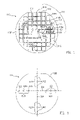
- FIG. 1 is a top plan view of a wafer in accordance with one embodiment of the present invention.
- FIG. 2 is a cross-sectional view of the wafer along the line II—II of FIG. 1 in accordance with one embodiment of the present invention.
- FIG. 3 is a bottom plan view of the wafer of FIG. 1 in accordance with one embodiment of the present invention.
- FIG. 4 is a cross-sectional view of the wafer during singulation processing in accordance with one embodiment of the present invention.
- FIG. 5 is a cross-sectional view of the wafer of FIG. 4 at a further stage during singulation processing in accordance with one embodiment of the present invention.
- FIG. 6 is a cross-sectional view of the wafer of FIG. 5 at a further stage during singulation processing in accordance with one embodiment of the present invention.
- FIG. 7 is a cross-sectional view of the wafer of FIG. 6 at a further stage during singulation processing in accordance with one embodiment of the present invention.
- integrated circuits 112 of a wafer 110 are delineated by a scribe grid 116 on a front-side surface 110 F of wafer 110 .
- Scribe grid 116 includes vertical scribe lines 114 and horizontal scribe lines 115 .
- a wafer support 204 e.g., a sticky tape, is adhesively attached to front-side surface 110 F of wafer 110 ( FIG. 4 ) to protect front-side surface 110 F during singulation of wafer 110 .
- Wafer 110 is drilled all the way through from front-side surface 110 F to a back-side surface 110 B of wafer 110 with drill bit 502 ( FIG. 5 ) to form back-side alignment marks 162 on back-side surface 110 of wafer 110 ( FIG. 3 ).
- a saw 622 ( FIGS. 1 , 6 ) is aligned with scribe grid 116 using back-side alignment marks 162 .
- Wafer 110 is cut from back-side surface 110 B with saw 622 along scribe grid 116 to singulate wafer 110 .
- wafer 110 is cut from back-side surface 110 B and wafer support 204 protects front-side surface 110 F of wafer 110 during singulation. Further, since back-side alignment marks 162 are positioned with respect to scribe grid 116 to within tight tolerance, wafer 110 is singulated precisely along scribe grid 116 . Accordingly, wafer 110 is not fabricated with the extra large width of scribe lines of conventional wafers designed to be cut from the back-side surface.
- FIG. 1 is a top plan view of a wafer 110 , e.g., a substrate, in accordance with the present invention.
- a wafer 110 e.g., a substrate
- integrated circuits 112 are formed in wafer 110 .
- integrated circuits 112 are set forth as the electronic components formed in wafer 110 , electronic components such as micromachine chips or image sensor chips are formed in wafer 110 instead of integrated circuits 112 in other embodiments.
- integrated circuits 112 are discussed below and illustrated in the figures.
- a scribe grid 116 e.g., a reference feature, on a front-side, e.g., first, surface 110 F of wafer 110 delineates integrated circuits 112 .
- scribe grid 116 is a silicon oxide layer, which has been selectively etched, on front-side surface 110 F.
- Integrated circuits 112 include integrated circuits 112 A, 112 B, 112 C, 112 D and 112 E.
- Scribe grid 116 includes a plurality of vertical scribe lines 114 and a plurality of horizontal scribe lines 115 , which delineate adjacent integrated circuits 112 .
- vertical scribe lines 114 extend in a first direction, e.g., vertical in the view of FIG. 1 .
- horizontal scribe lines 115 extend in a second direction perpendicular to the first direction, e.g., horizontal in the view of FIG. 1 .
- wafer 110 includes a flat 113 , which is a cut straight edge of wafer 110 .
- Flat 113 extends in the second direction, e.g., horizontal in the view of FIG. 1 .
- a first vertical scribe line 114 A of the plurality of vertical scribe lines 114 delineates integrated circuit 112 A, e.g., a first integrated circuit 112 , from integrated circuit 112 B, e.g., a second integrated circuit 112 .
- a first horizontal scribe line 115 A of the plurality of horizontal scribe lines 115 delineates integrated circuit 112 B from integrated circuit 112 C, e.g., a third integrated circuit 112 .
- a second vertical scribe line 114 B of the plurality of vertical scribe lines 114 delineates integrated circuit 112 B from integrated circuit 112 D, e.g., a forth integrated circuit 112 .
- first back-side alignment mark 162 A of a plurality of back-side alignment marks 162 of wafer 110 is formed at the intersection of vertical scribe line 114 A and horizontal scribe line 115 A.
- second back-side alignment mark 162 B of the plurality of back-side alignment marks 162 of wafer 110 is formed at the intersection of vertical scribe line 114 B and horizontal scribe line 115 A.
- FIG. 2 is a cross-sectional view of wafer 110 along the line II—II of FIG. 1 in accordance with one embodiment of the present invention.
- a wafer support 204 is attached, e.g., adhesively, to front-side surface 110 F of wafer 110 . More particularly, an adhesive interior, e.g., first, surface 204 I of wafer support 204 is attached to front-side surface 110 F of wafer 110 . Wafer support 204 is not illustrated in FIG. 1 for purposes of clarity.
- wafer support 204 is a sticky tape commonly used during wafer singulation as is well known to those of skill in the art.
- wafer support 204 is a blue or clear sticky tape such as those available from NITTO or LINTEC, respectively, although other supportive materials are used in other embodiments.
- wafer support 204 is sufficiently transparent to allow optical recognition, e.g., by the operator or alignment system, of scribe grid 116 through wafer support 204 .
- Wafer support 204 is a single integral layer or, alternatively, is two or more layers connected together.
- wafer support 204 is ultraviolet radiation (UV) curable. More particularly, upon irradiating wafer support 204 with ultraviolet radiation, wafer support 204 becomes polymerized such that adhesive interior surface 204 I of wafer support 204 becomes nonadhesive and is easily detached from front-side surface 110 F of wafer 110 .
- UV ultraviolet radiation
- Each integrated circuit 112 includes one or more bond pads 240 on front-side surface 110 F. Bond pads 240 are used to form the electrical interconnections with the internal circuitry (not shown) of integrated circuits 112 as is well known to those of skill in the art.
- integrated circuit 112 A includes a first bond pad 240 A and a second bond pad 240 B of a plurality of bond pads 240 on a front-side surface 112 F of integrated circuit 112 A.
- the other integrated circuits 112 include bond pads 240 in a similar manner so are not discussed further to avoid detracting from the principals of the invention.
- wafer 110 is an image sensor substrate and integrated circuits 112 are image sensor chips, sometimes called optical chips.
- integrated circuits 112 include active areas 242 on front-side surface 110 F.
- integrated circuit 112 A includes an active area 242 A on front-side surface 112 F of integrated circuit 112 A.
- the other integrated circuits 112 include active areas 242 in a similar manner so are not discussed further to avoid detracting from the principals of the invention.
- active areas 242 receive radiation, transmit radiation, or receive and transmit radiation, i.e., are transceivers. Active areas 242 and bond pads 240 are not illustrated in FIG. 1 for purposes of clarity.
- wafer 110 is a micromachine substrate and integrated circuits 112 are micromachine chips, sometimes called microelectromechanical systems (MEMS).
- MEMS microelectromechanical systems
- active areas 242 contain miniature movable structures, sometimes called micromachines.
- integrated circuits 112 are vertical cavity surface emitting lasers (VCSEL) chips.
- VCSEL vertical cavity surface emitting lasers
- cavities 206 are formed in wafer support 204 and these cavities 206 are aligned above active areas 242 .
- Cavities 206 can be formed using a wide variety of techniques, e.g., such as that set forth in Roberts, Jr. et al., cited above.
- back-side alignment mark 162 A is an aperture extending through wafer support 204 , i.e., from an exterior, e.g., second, surface 204 E of wafer support 204 to interior surface 204 I, and extending through wafer 110 , i.e., from front-side surface 110 F to a back-side, e.g., second, surface 110 B of wafer 110 . More generally, back-side alignment mark 162 A extends from exterior surface 204 E of wafer support 204 to back-side surface 110 B of wafer 110 . Similarly, back-side alignment mark 162 B extends from exterior surface 204 E to back-side surface 110 B. Back-side alignment marks 162 A, 162 B are perpendicular to exterior surface 204 E, interior surface 204 I, front-side surface 110 F and back-side surface 110 B, which are parallel to one another.
- back-side alignment marks 162 are similar to back-side alignment marks 162 A, 162 B and so are not discussed further to avoid detracting from the principals of the invention.
- back-side alignment marks 162 have a diameter of 0.001 inches (0.0254 millimeters) although back-side alignment marks 162 have other dimensions in other embodiments.
- FIG. 3 is a bottom plan view of wafer 110 of FIG. 1 in accordance with this embodiment of the present invention. Referring now to FIGS. 1 and 3 together, back-side alignment marks 162 form a pattern on back-side surface 110 B.
- back-side alignment mark 162 is formed, e.g., back-side alignment mark 162 A.
- back-side alignment mark 162 A has a positional relationship to scribe grid 116 .
- the position of back-side alignment mark 162 A is related to the position of scribe grid 116 such that by knowing the position of back-side alignment mark 162 A the position of scribe grid 116 is readily determined. More particularly, back-side alignment mark 162 A is directly aligned with the intersection of vertical scribe line 114 A and horizontal scribe line 115 A.
- twelve back-side alignment marks 162 are formed. More particularly, six back-side alignment marks 162 H, which form a first set of the plurality of back-side alignment marks 162 , are directly aligned with horizontal scribe line 115 A. Similarly, six back-side alignment marks 162 V, which form a second set of the plurality of back-side alignment marks 162 , are directly aligned with a vertical scribe line 114 C of the plurality of vertical scribe lines 114 .
- back-side alignment marks 162 H, 162 V define horizontal line 302 , vertical line 304 , respectively.
- Horizontal line 302 is precisely aligned with horizontal scribe line 115 A.
- Vertical line 304 is precisely aligned with vertical scribe line 114 C.
- this allows wafer 110 to be precisely singulated along scribe grid 116 from back-side surface 110 B using back-side alignment marks 162 as described further below.
- a back-side alignment mark is formed at each intersection of a vertical scribe lines 114 with a horizontal scribe line 115 .
- FIG. 4 is a cross-sectional view of wafer 110 during singulation processing in accordance with one embodiment of the present invention.
- FIG. 4 is substantially similar to FIG. 2 and only the significant differences are discussed below.
- interior surface 204 I of wafer support 204 is adhesively attached to front-side surface 110 F of wafer 110 .
- wafer support 204 is mounted to wafer 110 .
- wafer support 204 is mounted to wafer 110 without any alignment.
- wafer 110 is formed without active areas 242 , or, alternatively, active areas 242 can be contacted without causing any damage or destruction.
- wafer support 204 is mounted to wafer 110 without any alignment.
- wafer support 204 is formed with cavities 206 in interior surface 204 I.
- wafer support 204 is aligned, e.g., optically or mechanically, with wafer 110 such that cavities 206 are aligned above active areas 242 .
- wafer support 204 is illustrated without cavities 206 although it is understood that wafer support 204 would include cavities 206 depending upon the particular application.
- FIG. 5 is a cross-sectional view of wafer 110 of FIG. 4 at a further stage during singulation processing in accordance with this embodiment of the present invention.
- a drill bit 502 is aligned at a first intersection of particular vertical scribe line 114 and a particular horizontal scribe line 115 .
- Drill bit 502 drills through wafer 110 at the first intersection to form a first back-side alignment mark 162 .
- drill bit 502 is aligned at the intersection of vertical scribe line 114 A and horizontal scribe line 115 A.
- Drill bit 502 drills through wafer 110 from front-side surface 110 F to back-side surface 110 B at the intersection of vertical scribe line 114 A and horizontal scribe line 115 A to form back-side alignment mark 162 A.
- Drill bit 502 is realigned at a second intersection of another particular vertical scribe line 114 and another particular horizontal scribe line 115 . Drill bit 502 drills through wafer 110 from front-side surface 110 F to back-side surface 110 B at the second intersection to form a second back-side alignment mark 162 .
- drill bit 502 is aligned at the intersection of vertical scribe line 114 B and horizontal scribe line 115 A.
- Drill bit 502 drills through wafer 110 as shown in FIG. 5 at the intersection of vertical scribe line 114 B and horizontal scribe line 115 A to form back-side alignment mark 162 B. This iterative process is repeated until all back-side alignment marks 162 are formed.
- a plurality of drill bits 502 are used to form back-side alignment marks 162 simultaneously.
- a laser, a high-pressure water drill, or other drilling device is used to form back-side alignment marks 162 .
- wafer support 204 is sufficiently transparent to allow optical recognition of scribe grid 116 , i.e., vertical scribe lines 114 and horizontal scribe lines 115 , through wafer support 204 . Accordingly, scribe grid 116 is used directly to align drill bit 502 and form back-side alignment marks 162 . This allows back-side alignment marks 162 to be formed in precise alignment with scribe grid 116 .
- wafer support 204 protects front-side surface 110 F of wafer 110 during formation of align marks 162 . More particularly, wafer support 204 prevents slag and silicon shards 504 , i.e., contaminants, generated during formation of back-side alignment marks 162 from contacting front-side surface 110 F of wafer 110 . In this manner, damage or destruction of integrated circuits 112 is prevented. This, in turn, increases yield, which decreases the fabrication cost of each integrated circuit 112 .
- slag and silicon shards 504 are removed using a high-pressure wash immediately after formation of alignment marks 162 .
- slag and silicon shards 504 are removed after subsequent singulation processing described further below.
- FIG. 6 is a cross-sectional view of wafer 110 of FIG. 5 at a further stage during singulation processing in accordance with this embodiment of the present invention.
- wafer 110 is inverted from the view of FIG. 5 .
- Wafer support 204 is mounted to a sawing chuck 602 , e.g., using vacuum in a conventional manner. More particularly, exterior surface 204 E of wafer support 204 is mounted to sawing chuck 602 .
- a saw 622 e.g., the blade of a mechanical saw, is aligned with a vertical scribe line 114 D, which delineates integrated circuit 112 A from integrated circuit 112 E as best shown in FIG. 1 .
- Saw 622 is aligned with vertical scribe line 114 D using one or more back-side alignment marks 162 (hereinafter referred to as back-side alignment mark 162 for simplicity) as a reference, e.g., see back-side alignment marks 162 of FIG. 3 .
- back-side alignment mark 162 back-side alignment mark 162
- light is shined at an angle to back-side surface 110 B to enhance the contrast between alignment mark 162 and the bulk of back-side surface 110 B to enhance recognition of alignment mark 162 .
- the position of vertical scribe line 114 D is determined from back-side alignment mark 162 and this information is used to align saw 622 with vertical scribe line 114 D.
- an optical or mechanical alignment system which is well known to those of skill in the art, aligns saw 622 with vertical scribe line 114 D using back-side alignment mark 162 as a reference.
- back-side alignment mark 162 is positioned with respect to vertical scribe line 114 D to within tight tolerance, e.g., to within 0.001 in. (0.025 mm) or less
- saw 622 is precisely aligned to vertical scribe line 114 D.
- Wafer 110 is cut from back-side surface 110 B along vertical scribe line 114 D with saw 622 .
- cutting of wafer 110 with saw 622 e.g., the blade of a mechanical saw
- saw 622 as used herein includes a mechanical saw, a laser saw and a high-pressure water saw as well as other comparable saws.
- saw 622 is precisely aligned to vertical scribe line 114 D such that wafer 110 is precisely cut along vertical scribe line 114 D. Since wafer 110 is precisely cut along vertical scribe line 114 D, vertical scribe line 114 D is not fabricated with the extra large width of scribe lines of conventional wafers designed to be cut from the back-side surface. Accordingly, vertical scribe line 114 D is relatively narrow and has a narrow width W.
- width W of vertical scribe line 114 D is the same as the width of a scribe line of a wafer, which was designed to be cut from the front-side surface of the wafer.
- width W is in the range of approximately 0.002 inches (0.051 mm) to 0.008 inches (0.203 mm) and in one particular embodiment is within the range of 0.002 inches (0.051 mm) to 0.003 inches (0.076 mm) or less although width W has other dimensions in other embodiments.
- wafer 110 is cut along scribe lines 114 and 115 ( FIG. 1 ), i.e., along scribe grid 116 , using back-side alignment mark 162 as a reference in a similar manner to that described above with regard to vertical scribe line 114 D.
- Saw 622 cuts wafer 110 from back-side surface 110 B along scribe grid 116 thus singulating integrated circuits 112 .
- wafer 110 is stepped, i.e., moved a fixed distance, such that saw 622 is precisely aligned with the adjacent singulation street 114 (or 115 ).
- the adjacent singulation street 114 (or 115 ) is then sawed. This iterative process is repeated until all of singulation streets 114 (or 115 ) are sawed. Wafer 110 is then rotated 90°.
- wafer 110 After rotation of wafer 110 , another particular singulation street 115 (or 114 ) of the plurality of singulation streets 115 (or 114 ) is sawed. After sawing of the particular singulation street 115 (or 114 ), wafer 110 is stepped, i.e., moved a fixed distance, such that saw 622 is precisely aligned with the adjacent singulation street 115 (or 114 ). The adjacent singulation street 115 (or 114 ) is then sawed. This iterative process is repeated until all of singulation street 115 (or 114 ) are sawed and wafer 110 is singulated.
- wafer 110 is cut from back-side surface 110 B thus protecting front-side surface 110 F of wafer 110 .
- wafer support 204 prevents slag and silicon shards 604 , i.e., contaminants, generated during singulation of wafer 110 from contacting front-side surface 110 F of wafer 110 . In this manner, damage or destruction of integrated circuits 112 is prevented. This, in turn, increases yield, which decreases the fabrication cost of each integrated circuit 112 .
- width W of scribe lines 114 , 115 is significantly less than that of conventional wafers designed to be cut from the back-side surface.
- the wafer designed to be cut from the back-side surface was formed with relatively wide scribe lines.
- forming the scribe lines with a relatively large width resulted in less integrated circuits for any given size wafer, i.e., a loss of yield. This resulted in a substantial increase in the cost of the integrated circuits in the prior art.
- wafer 110 is cut from back-side surface 110 B without the associated loss of yield of the prior art.
- integrated circuits 112 of wafer 110 are protected during singulation yet are fabricated without the associated substantial increase in cost of the prior art.
- FIG. 7 is a cross-sectional view of wafer 110 of FIG. 6 at a further stage during singulation processing in accordance with this embodiment of the present invention.
- wafer 110 is high pressure washed to remove any slag and silicon shards 604 ( FIG. 6 ) generated during singulation of wafer 110 .
- a vacuum pickup head 702 of a pick and place machine 704 attaches to back-side surface 112 B of integrated circuit 112 A, and more generally to back-side surface 110 B of wafer 110 .
- Pick and place machine 704 removes integrated circuit 112 A from wafer support 204 .
- Integrated circuit 112 A is either packaged for shipment or further processed as is well known to those of skill in the art.
- the other integrated circuits 112 are similarly removed from wafer support 204 by pick and place machine 704 .
- front-side surfaces 112 F of integrated circuits 112 is clean and free from slag and silicon shards.
- integrated circuits 112 are flipped over after being removed from wafer support 204 and placed for die attach and wirebonding. Die attach and wirebonding of integrated circuits are well known to those of skill in the art is not discussed further to avoid detracting from the principals of the invention.
- wafer support 204 is UV curable. In accordance with this embodiment, wafer support 204 is irradiated with ultraviolet radiation to polymerize wafer support 204 and render interior surface 204 I nonadhesive. Accordingly, integrated circuits 112 lose the adhesive mounting to wafer support 204 thus facilitating removal of integrated circuits 112 from wafer support 204 .
Abstract
Description
Claims (30)
Priority Applications (1)
| Application Number | Priority Date | Filing Date | Title |
|---|---|---|---|
| US09/803,084 US6943429B1 (en) | 2001-03-08 | 2001-03-08 | Wafer having alignment marks extending from a first to a second surface of the wafer |
Applications Claiming Priority (1)
| Application Number | Priority Date | Filing Date | Title |
|---|---|---|---|
| US09/803,084 US6943429B1 (en) | 2001-03-08 | 2001-03-08 | Wafer having alignment marks extending from a first to a second surface of the wafer |
Publications (1)
| Publication Number | Publication Date |
|---|---|
| US6943429B1 true US6943429B1 (en) | 2005-09-13 |
Family
ID=34912636
Family Applications (1)
| Application Number | Title | Priority Date | Filing Date |
|---|---|---|---|
| US09/803,084 Expired - Fee Related US6943429B1 (en) | 2001-03-08 | 2001-03-08 | Wafer having alignment marks extending from a first to a second surface of the wafer |
Country Status (1)
| Country | Link |
|---|---|
| US (1) | US6943429B1 (en) |
Cited By (46)
| Publication number | Priority date | Publication date | Assignee | Title |
|---|---|---|---|---|
| US20070264798A1 (en) * | 2006-04-14 | 2007-11-15 | Taiwan Semiconductor Manufacturing Company, Ltd. | Method and System for Partially Removing Circuit Patterns From a Multi-Project Wafer |
| US20090081828A1 (en) * | 2007-09-26 | 2009-03-26 | Northrop Grumman Systems Corporation | MEMS Fabrication Method |
| US20090079038A1 (en) * | 2007-09-20 | 2009-03-26 | Infineon Technologies Ag | Method Of Making An Integrated Circuit Including Singulating A Semiconductor Wafer |
| US8354678B1 (en) | 2011-07-11 | 2013-01-15 | International Business Machines Corporation | Structure and method for forming a light detecting diode and a light emitting diode on a silicon-on-insulator wafer backside |
| CN103137633A (en) * | 2011-11-28 | 2013-06-05 | 台湾积体电路制造股份有限公司 | Dark current reduction of back side illuminated image sensor |
| US20140137794A1 (en) * | 2012-11-19 | 2014-05-22 | Memc Singapore, Pte. Ltd (Uen200614797D) | Method of Preparing A Directional Solidification System Furnace |
| US20160126196A1 (en) | 2014-11-03 | 2016-05-05 | Rf Micro Devices, Inc. | Printed circuit module having a semiconductor device with a protective layer in place of a low-resistivity handle layer |
| US9366524B2 (en) | 2013-10-08 | 2016-06-14 | Kla-Tencor Corporation | Alignment sensor and height sensor |
| US9583414B2 (en) | 2013-10-31 | 2017-02-28 | Qorvo Us, Inc. | Silicon-on-plastic semiconductor device and method of making the same |
| US9613831B2 (en) | 2015-03-25 | 2017-04-04 | Qorvo Us, Inc. | Encapsulated dies with enhanced thermal performance |
| US9812350B2 (en) | 2013-03-06 | 2017-11-07 | Qorvo Us, Inc. | Method of manufacture for a silicon-on-plastic semiconductor device with interfacial adhesion layer |
| US9824951B2 (en) | 2014-09-12 | 2017-11-21 | Qorvo Us, Inc. | Printed circuit module having semiconductor device with a polymer substrate and methods of manufacturing the same |
| US20170358511A1 (en) | 2016-06-10 | 2017-12-14 | Qorvo Us, Inc. | Thermally enhanced semiconductor package with thermal additive and process for making the same |
| US20180019184A1 (en) | 2016-07-18 | 2018-01-18 | Qorvo Us, Inc. | Thermally enhanced semiconductor package having field effect transistors with back-gate feature |
| US20180044177A1 (en) | 2016-08-12 | 2018-02-15 | Qorvo Us, Inc. | Wafer-level package with enhanced performance |
| US9960145B2 (en) | 2015-03-25 | 2018-05-01 | Qorvo Us, Inc. | Flip chip module with enhanced properties |
| US10020405B2 (en) | 2016-01-19 | 2018-07-10 | Qorvo Us, Inc. | Microelectronics package with integrated sensors |
| US10038055B2 (en) | 2015-05-22 | 2018-07-31 | Qorvo Us, Inc. | Substrate structure with embedded layer for post-processing silicon handle elimination |
| US20180228030A1 (en) | 2014-10-01 | 2018-08-09 | Qorvo Us, Inc. | Method for manufacturing an integrated circuit package |
| US10062583B2 (en) | 2016-05-09 | 2018-08-28 | Qorvo Us, Inc. | Microelectronics package with inductive element and magnetically enhanced mold compound component |
| US10068831B2 (en) | 2016-12-09 | 2018-09-04 | Qorvo Us, Inc. | Thermally enhanced semiconductor package and process for making the same |
| US10090339B2 (en) | 2016-10-21 | 2018-10-02 | Qorvo Us, Inc. | Radio frequency (RF) switch |
| US10109502B2 (en) | 2016-09-12 | 2018-10-23 | Qorvo Us, Inc. | Semiconductor package with reduced parasitic coupling effects and process for making the same |
| US10109550B2 (en) | 2016-08-12 | 2018-10-23 | Qorvo Us, Inc. | Wafer-level package with enhanced performance |
| US20190013255A1 (en) | 2017-07-06 | 2019-01-10 | Qorvo Us, Inc. | Wafer-level packaging for enhanced performance |
| US20190074263A1 (en) | 2017-09-05 | 2019-03-07 | Qorvo Us, Inc. | Microelectronics package with self-aligned stacked-die assembly |
| US20190074271A1 (en) | 2017-09-05 | 2019-03-07 | Qorvo Us, Inc. | Microelectronics package with self-aligned stacked-die assembly |
| US10276495B2 (en) | 2015-09-11 | 2019-04-30 | Qorvo Us, Inc. | Backside semiconductor die trimming |
| US10486963B2 (en) | 2016-08-12 | 2019-11-26 | Qorvo Us, Inc. | Wafer-level package with enhanced performance |
| US20200235054A1 (en) | 2019-01-23 | 2020-07-23 | Qorvo Us, Inc. | Rf devices with enhanced performance and methods of forming the same |
| US10749518B2 (en) | 2016-11-18 | 2020-08-18 | Qorvo Us, Inc. | Stacked field-effect transistor switch |
| US10773952B2 (en) | 2016-05-20 | 2020-09-15 | Qorvo Us, Inc. | Wafer-level package with enhanced performance |
| US10784149B2 (en) | 2016-05-20 | 2020-09-22 | Qorvo Us, Inc. | Air-cavity module with enhanced device isolation |
| US10804246B2 (en) | 2018-06-11 | 2020-10-13 | Qorvo Us, Inc. | Microelectronics package with vertically stacked dies |
| US10964554B2 (en) | 2018-10-10 | 2021-03-30 | Qorvo Us, Inc. | Wafer-level fan-out package with enhanced performance |
| CN112885241A (en) * | 2021-02-07 | 2021-06-01 | 业成科技(成都)有限公司 | Frame and manufacturing method thereof, display module and measuring method thereof and electronic equipment |
| US11069590B2 (en) | 2018-10-10 | 2021-07-20 | Qorvo Us, Inc. | Wafer-level fan-out package with enhanced performance |
| US20210242364A1 (en) * | 2020-01-31 | 2021-08-05 | Nichia Corporation | Method of producing light-emitting device |
| US20210296199A1 (en) | 2018-11-29 | 2021-09-23 | Qorvo Us, Inc. | Thermally enhanced semiconductor package with at least one heat extractor and process for making the same |
| US11152363B2 (en) | 2018-03-28 | 2021-10-19 | Qorvo Us, Inc. | Bulk CMOS devices with enhanced performance and methods of forming the same utilizing bulk CMOS process |
| US11387157B2 (en) | 2019-01-23 | 2022-07-12 | Qorvo Us, Inc. | RF devices with enhanced performance and methods of forming the same |
| US11646289B2 (en) | 2019-12-02 | 2023-05-09 | Qorvo Us, Inc. | RF devices with enhanced performance and methods of forming the same |
| US11705428B2 (en) | 2019-01-23 | 2023-07-18 | Qorvo Us, Inc. | RF devices with enhanced performance and methods of forming the same |
| US11710680B2 (en) | 2019-01-23 | 2023-07-25 | Qorvo Us, Inc. | RF devices with enhanced performance and methods of forming the same |
| US11923238B2 (en) | 2019-12-12 | 2024-03-05 | Qorvo Us, Inc. | Method of forming RF devices with enhanced performance including attaching a wafer to a support carrier by a bonding technique without any polymer adhesive |
| US11961813B2 (en) | 2022-01-11 | 2024-04-16 | Qorvo Us, Inc. | RF devices with enhanced performance and methods of forming the same |
Citations (27)
| Publication number | Priority date | Publication date | Assignee | Title |
|---|---|---|---|---|
| JPS6042846A (en) * | 1983-08-18 | 1985-03-07 | Nec Kansai Ltd | Dicing method for semiconductor wafer |
| US5362681A (en) * | 1992-07-22 | 1994-11-08 | Anaglog Devices, Inc. | Method for separating circuit dies from a wafer |
| JPH07273069A (en) * | 1994-03-31 | 1995-10-20 | Nichia Chem Ind Ltd | Manufacture of gallium nitride compound semiconductor chip |
| US5777392A (en) * | 1995-03-28 | 1998-07-07 | Nec Corporation | Semiconductor device having improved alignment marks |
| US5888884A (en) | 1998-01-02 | 1999-03-30 | General Electric Company | Electronic device pad relocation, precision placement, and packaging in arrays |
| US6071656A (en) * | 1999-07-07 | 2000-06-06 | United Microelectronics Corp. | Photolithography technique utilizing alignment marks at scribe line intersections |
| US6102775A (en) * | 1997-04-18 | 2000-08-15 | Nikon Corporation | Film inspection method |
| US6132910A (en) * | 1997-12-04 | 2000-10-17 | Nec Corporation | Method of implementing electron beam lithography using uniquely positioned alignment marks and a wafer with such alignment marks |
| US6151344A (en) | 1998-03-30 | 2000-11-21 | Motorola, Inc. | Automatic power control of semiconductor laser |
| US6151120A (en) * | 1997-11-26 | 2000-11-21 | Canon Kabushiki Kaisha | Exposure apparatus and method |
| US6275277B1 (en) * | 1999-05-17 | 2001-08-14 | Colorado Microdisplay, Inc. | Micro liquid crystal displays having a circular cover glass and a viewing area free of spacers |
| US6316334B1 (en) * | 1999-04-12 | 2001-11-13 | Tanner Research, Inc. | Method of fabricating various-sized passivated integrated circuit chips from a borderless gate array |
| US20010040224A1 (en) * | 1997-11-14 | 2001-11-15 | Takahiro Matsumoto | Positional deviation detecting method and device manufacturing method using the same |
| US6340547B1 (en) * | 2000-01-11 | 2002-01-22 | Taiwan Semiconductor Manufacturing Company, Ltd | Method of forming circuit patterns on semiconductor wafers using two optical steppers having nonaligned imaging systems |
| US20020031899A1 (en) * | 1999-06-08 | 2002-03-14 | Ran Manor | Apparatus and method for singulating semiconductor wafers |
| US6407360B1 (en) * | 1998-08-26 | 2002-06-18 | Samsung Electronics, Co., Ltd. | Laser cutting apparatus and method |
| US6421456B1 (en) * | 1997-12-23 | 2002-07-16 | Samsung Electronics Co., Ltd. | Semiconductor wafer on which recognition marks are formed and method for sawing the wafer using the recognition marks |
| US6420776B1 (en) * | 2001-03-01 | 2002-07-16 | Amkor Technology, Inc. | Structure including electronic components singulated using laser cutting |
| US6441504B1 (en) * | 2000-04-25 | 2002-08-27 | Amkor Technology, Inc. | Precision aligned and marked structure |
| US6465329B1 (en) * | 1999-01-20 | 2002-10-15 | Amkor Technology, Inc. | Microcircuit die-sawing protector and method |
| US6476415B1 (en) * | 2000-07-20 | 2002-11-05 | Three-Five Systems, Inc. | Wafer scale processing |
| US6492189B1 (en) * | 1999-11-09 | 2002-12-10 | Kawasaki Microelectronics, Inc. | Method of arranging exposed areas including a limited number of test element group (TEG) regions on a semiconductor wafer |
| US6528393B2 (en) * | 2000-06-13 | 2003-03-04 | Advanced Semiconductor Engineering, Inc. | Method of making a semiconductor package by dicing a wafer from the backside surface thereof |
| US20030054588A1 (en) * | 2000-12-07 | 2003-03-20 | Reflectivity, Inc., A California Corporation | Methods for depositing, releasing and packaging micro-electromechanical devices on wafer substrates |
| US6537836B2 (en) | 1999-07-28 | 2003-03-25 | Infineon Technologies Ag | Semiconductor structures and manufacturing methods |
| JP2003188263A (en) * | 2001-12-17 | 2003-07-04 | Sharp Corp | Method for producing semiconductor integrated circuit chip and semiconductor package using semiconductor integrated circuit chip |
| US20030140514A1 (en) * | 2002-01-28 | 2003-07-31 | Chien-Chih Fu | Scribe lines for increasing wafer utilizable area |
-
2001
- 2001-03-08 US US09/803,084 patent/US6943429B1/en not_active Expired - Fee Related
Patent Citations (27)
| Publication number | Priority date | Publication date | Assignee | Title |
|---|---|---|---|---|
| JPS6042846A (en) * | 1983-08-18 | 1985-03-07 | Nec Kansai Ltd | Dicing method for semiconductor wafer |
| US5362681A (en) * | 1992-07-22 | 1994-11-08 | Anaglog Devices, Inc. | Method for separating circuit dies from a wafer |
| JPH07273069A (en) * | 1994-03-31 | 1995-10-20 | Nichia Chem Ind Ltd | Manufacture of gallium nitride compound semiconductor chip |
| US5777392A (en) * | 1995-03-28 | 1998-07-07 | Nec Corporation | Semiconductor device having improved alignment marks |
| US6102775A (en) * | 1997-04-18 | 2000-08-15 | Nikon Corporation | Film inspection method |
| US20010040224A1 (en) * | 1997-11-14 | 2001-11-15 | Takahiro Matsumoto | Positional deviation detecting method and device manufacturing method using the same |
| US6151120A (en) * | 1997-11-26 | 2000-11-21 | Canon Kabushiki Kaisha | Exposure apparatus and method |
| US6132910A (en) * | 1997-12-04 | 2000-10-17 | Nec Corporation | Method of implementing electron beam lithography using uniquely positioned alignment marks and a wafer with such alignment marks |
| US6421456B1 (en) * | 1997-12-23 | 2002-07-16 | Samsung Electronics Co., Ltd. | Semiconductor wafer on which recognition marks are formed and method for sawing the wafer using the recognition marks |
| US5888884A (en) | 1998-01-02 | 1999-03-30 | General Electric Company | Electronic device pad relocation, precision placement, and packaging in arrays |
| US6151344A (en) | 1998-03-30 | 2000-11-21 | Motorola, Inc. | Automatic power control of semiconductor laser |
| US6407360B1 (en) * | 1998-08-26 | 2002-06-18 | Samsung Electronics, Co., Ltd. | Laser cutting apparatus and method |
| US6465329B1 (en) * | 1999-01-20 | 2002-10-15 | Amkor Technology, Inc. | Microcircuit die-sawing protector and method |
| US6316334B1 (en) * | 1999-04-12 | 2001-11-13 | Tanner Research, Inc. | Method of fabricating various-sized passivated integrated circuit chips from a borderless gate array |
| US6275277B1 (en) * | 1999-05-17 | 2001-08-14 | Colorado Microdisplay, Inc. | Micro liquid crystal displays having a circular cover glass and a viewing area free of spacers |
| US20020031899A1 (en) * | 1999-06-08 | 2002-03-14 | Ran Manor | Apparatus and method for singulating semiconductor wafers |
| US6071656A (en) * | 1999-07-07 | 2000-06-06 | United Microelectronics Corp. | Photolithography technique utilizing alignment marks at scribe line intersections |
| US6537836B2 (en) | 1999-07-28 | 2003-03-25 | Infineon Technologies Ag | Semiconductor structures and manufacturing methods |
| US6492189B1 (en) * | 1999-11-09 | 2002-12-10 | Kawasaki Microelectronics, Inc. | Method of arranging exposed areas including a limited number of test element group (TEG) regions on a semiconductor wafer |
| US6340547B1 (en) * | 2000-01-11 | 2002-01-22 | Taiwan Semiconductor Manufacturing Company, Ltd | Method of forming circuit patterns on semiconductor wafers using two optical steppers having nonaligned imaging systems |
| US6441504B1 (en) * | 2000-04-25 | 2002-08-27 | Amkor Technology, Inc. | Precision aligned and marked structure |
| US6528393B2 (en) * | 2000-06-13 | 2003-03-04 | Advanced Semiconductor Engineering, Inc. | Method of making a semiconductor package by dicing a wafer from the backside surface thereof |
| US6476415B1 (en) * | 2000-07-20 | 2002-11-05 | Three-Five Systems, Inc. | Wafer scale processing |
| US20030054588A1 (en) * | 2000-12-07 | 2003-03-20 | Reflectivity, Inc., A California Corporation | Methods for depositing, releasing and packaging micro-electromechanical devices on wafer substrates |
| US6420776B1 (en) * | 2001-03-01 | 2002-07-16 | Amkor Technology, Inc. | Structure including electronic components singulated using laser cutting |
| JP2003188263A (en) * | 2001-12-17 | 2003-07-04 | Sharp Corp | Method for producing semiconductor integrated circuit chip and semiconductor package using semiconductor integrated circuit chip |
| US20030140514A1 (en) * | 2002-01-28 | 2003-07-31 | Chien-Chih Fu | Scribe lines for increasing wafer utilizable area |
Cited By (79)
| Publication number | Priority date | Publication date | Assignee | Title |
|---|---|---|---|---|
| US7904855B2 (en) * | 2006-04-14 | 2011-03-08 | Taiwan Semiconductor Manufacturing Company, Ltd. | Methods for partially removing circuit patterns from a multi-project wafer |
| US20070264798A1 (en) * | 2006-04-14 | 2007-11-15 | Taiwan Semiconductor Manufacturing Company, Ltd. | Method and System for Partially Removing Circuit Patterns From a Multi-Project Wafer |
| US20090079038A1 (en) * | 2007-09-20 | 2009-03-26 | Infineon Technologies Ag | Method Of Making An Integrated Circuit Including Singulating A Semiconductor Wafer |
| US7674689B2 (en) | 2007-09-20 | 2010-03-09 | Infineon Technologies Ag | Method of making an integrated circuit including singulating a semiconductor wafer |
| US20090081828A1 (en) * | 2007-09-26 | 2009-03-26 | Northrop Grumman Systems Corporation | MEMS Fabrication Method |
| US8354678B1 (en) | 2011-07-11 | 2013-01-15 | International Business Machines Corporation | Structure and method for forming a light detecting diode and a light emitting diode on a silicon-on-insulator wafer backside |
| CN103137633A (en) * | 2011-11-28 | 2013-06-05 | 台湾积体电路制造股份有限公司 | Dark current reduction of back side illuminated image sensor |
| CN103137633B (en) * | 2011-11-28 | 2016-02-10 | 台湾积体电路制造股份有限公司 | Reduce the dark current of back side illumination image sensor |
| US20140137794A1 (en) * | 2012-11-19 | 2014-05-22 | Memc Singapore, Pte. Ltd (Uen200614797D) | Method of Preparing A Directional Solidification System Furnace |
| US9812350B2 (en) | 2013-03-06 | 2017-11-07 | Qorvo Us, Inc. | Method of manufacture for a silicon-on-plastic semiconductor device with interfacial adhesion layer |
| US10134627B2 (en) | 2013-03-06 | 2018-11-20 | Qorvo Us, Inc. | Silicon-on-plastic semiconductor device with interfacial adhesion layer |
| US9366524B2 (en) | 2013-10-08 | 2016-06-14 | Kla-Tencor Corporation | Alignment sensor and height sensor |
| US10062637B2 (en) | 2013-10-31 | 2018-08-28 | Qorvo Us, Inc. | Method of manufacture for a semiconductor device |
| US9583414B2 (en) | 2013-10-31 | 2017-02-28 | Qorvo Us, Inc. | Silicon-on-plastic semiconductor device and method of making the same |
| US9824951B2 (en) | 2014-09-12 | 2017-11-21 | Qorvo Us, Inc. | Printed circuit module having semiconductor device with a polymer substrate and methods of manufacturing the same |
| US10085352B2 (en) | 2014-10-01 | 2018-09-25 | Qorvo Us, Inc. | Method for manufacturing an integrated circuit package |
| US20180228030A1 (en) | 2014-10-01 | 2018-08-09 | Qorvo Us, Inc. | Method for manufacturing an integrated circuit package |
| US10492301B2 (en) | 2014-10-01 | 2019-11-26 | Qorvo Us, Inc. | Method for manufacturing an integrated circuit package |
| US10109548B2 (en) | 2014-11-03 | 2018-10-23 | Qorvo Us, Inc. | Printed circuit module having a semiconductor device with a protective layer in place of a low-resistivity handle layer |
| US10121718B2 (en) | 2014-11-03 | 2018-11-06 | Qorvo Us, Inc. | Printed circuit module having a semiconductor device with a protective layer in place of a low-resistivity handle layer |
| US10199301B2 (en) | 2014-11-03 | 2019-02-05 | Qorvo Us, Inc. | Methods of manufacturing a printed circuit module having a semiconductor device with a protective layer in place of a low-resistivity handle layer |
| US20160126196A1 (en) | 2014-11-03 | 2016-05-05 | Rf Micro Devices, Inc. | Printed circuit module having a semiconductor device with a protective layer in place of a low-resistivity handle layer |
| US9960145B2 (en) | 2015-03-25 | 2018-05-01 | Qorvo Us, Inc. | Flip chip module with enhanced properties |
| US10020206B2 (en) | 2015-03-25 | 2018-07-10 | Qorvo Us, Inc. | Encapsulated dies with enhanced thermal performance |
| US9613831B2 (en) | 2015-03-25 | 2017-04-04 | Qorvo Us, Inc. | Encapsulated dies with enhanced thermal performance |
| US10038055B2 (en) | 2015-05-22 | 2018-07-31 | Qorvo Us, Inc. | Substrate structure with embedded layer for post-processing silicon handle elimination |
| US10276495B2 (en) | 2015-09-11 | 2019-04-30 | Qorvo Us, Inc. | Backside semiconductor die trimming |
| US10020405B2 (en) | 2016-01-19 | 2018-07-10 | Qorvo Us, Inc. | Microelectronics package with integrated sensors |
| US10062583B2 (en) | 2016-05-09 | 2018-08-28 | Qorvo Us, Inc. | Microelectronics package with inductive element and magnetically enhanced mold compound component |
| US10090262B2 (en) | 2016-05-09 | 2018-10-02 | Qorvo Us, Inc. | Microelectronics package with inductive element and magnetically enhanced mold compound component |
| US10773952B2 (en) | 2016-05-20 | 2020-09-15 | Qorvo Us, Inc. | Wafer-level package with enhanced performance |
| US10882740B2 (en) | 2016-05-20 | 2021-01-05 | Qorvo Us, Inc. | Wafer-level package with enhanced performance and manufacturing method thereof |
| US10784149B2 (en) | 2016-05-20 | 2020-09-22 | Qorvo Us, Inc. | Air-cavity module with enhanced device isolation |
| US10103080B2 (en) | 2016-06-10 | 2018-10-16 | Qorvo Us, Inc. | Thermally enhanced semiconductor package with thermal additive and process for making the same |
| US20180197803A1 (en) | 2016-06-10 | 2018-07-12 | Qorvo Us, Inc. | Thermally enhanced semiconductor package with thermal additive and process for making the same |
| US20170358511A1 (en) | 2016-06-10 | 2017-12-14 | Qorvo Us, Inc. | Thermally enhanced semiconductor package with thermal additive and process for making the same |
| US10262915B2 (en) | 2016-06-10 | 2019-04-16 | Qorvo Us, Inc. | Thermally enhanced semiconductor package with thermal additive and process for making the same |
| US10468329B2 (en) | 2016-07-18 | 2019-11-05 | Qorvo Us, Inc. | Thermally enhanced semiconductor package having field effect transistors with back-gate feature |
| US10079196B2 (en) | 2016-07-18 | 2018-09-18 | Qorvo Us, Inc. | Thermally enhanced semiconductor package having field effect transistors with back-gate feature |
| US20180019184A1 (en) | 2016-07-18 | 2018-01-18 | Qorvo Us, Inc. | Thermally enhanced semiconductor package having field effect transistors with back-gate feature |
| US10804179B2 (en) | 2016-08-12 | 2020-10-13 | Qorvo Us, Inc. | Wafer-level package with enhanced performance |
| US10109550B2 (en) | 2016-08-12 | 2018-10-23 | Qorvo Us, Inc. | Wafer-level package with enhanced performance |
| US20180044177A1 (en) | 2016-08-12 | 2018-02-15 | Qorvo Us, Inc. | Wafer-level package with enhanced performance |
| US10486963B2 (en) | 2016-08-12 | 2019-11-26 | Qorvo Us, Inc. | Wafer-level package with enhanced performance |
| US10486965B2 (en) | 2016-08-12 | 2019-11-26 | Qorvo Us, Inc. | Wafer-level package with enhanced performance |
| US10985033B2 (en) | 2016-09-12 | 2021-04-20 | Qorvo Us, Inc. | Semiconductor package with reduced parasitic coupling effects and process for making the same |
| US10109502B2 (en) | 2016-09-12 | 2018-10-23 | Qorvo Us, Inc. | Semiconductor package with reduced parasitic coupling effects and process for making the same |
| US10090339B2 (en) | 2016-10-21 | 2018-10-02 | Qorvo Us, Inc. | Radio frequency (RF) switch |
| US10749518B2 (en) | 2016-11-18 | 2020-08-18 | Qorvo Us, Inc. | Stacked field-effect transistor switch |
| US20180342439A1 (en) | 2016-12-09 | 2018-11-29 | Qorvo Us, Inc. | Thermally enhanced semiconductor package and process for making the same |
| US10790216B2 (en) | 2016-12-09 | 2020-09-29 | Qorvo Us, Inc. | Thermally enhanced semiconductor package and process for making the same |
| US10068831B2 (en) | 2016-12-09 | 2018-09-04 | Qorvo Us, Inc. | Thermally enhanced semiconductor package and process for making the same |
| US10490471B2 (en) | 2017-07-06 | 2019-11-26 | Qorvo Us, Inc. | Wafer-level packaging for enhanced performance |
| US10755992B2 (en) | 2017-07-06 | 2020-08-25 | Qorvo Us, Inc. | Wafer-level packaging for enhanced performance |
| US20190013255A1 (en) | 2017-07-06 | 2019-01-10 | Qorvo Us, Inc. | Wafer-level packaging for enhanced performance |
| US10366972B2 (en) | 2017-09-05 | 2019-07-30 | Qorvo Us, Inc. | Microelectronics package with self-aligned stacked-die assembly |
| US10784233B2 (en) | 2017-09-05 | 2020-09-22 | Qorvo Us, Inc. | Microelectronics package with self-aligned stacked-die assembly |
| US20190074271A1 (en) | 2017-09-05 | 2019-03-07 | Qorvo Us, Inc. | Microelectronics package with self-aligned stacked-die assembly |
| US20190074263A1 (en) | 2017-09-05 | 2019-03-07 | Qorvo Us, Inc. | Microelectronics package with self-aligned stacked-die assembly |
| US11152363B2 (en) | 2018-03-28 | 2021-10-19 | Qorvo Us, Inc. | Bulk CMOS devices with enhanced performance and methods of forming the same utilizing bulk CMOS process |
| US11063021B2 (en) | 2018-06-11 | 2021-07-13 | Qorvo Us, Inc. | Microelectronics package with vertically stacked dies |
| US10804246B2 (en) | 2018-06-11 | 2020-10-13 | Qorvo Us, Inc. | Microelectronics package with vertically stacked dies |
| US11069590B2 (en) | 2018-10-10 | 2021-07-20 | Qorvo Us, Inc. | Wafer-level fan-out package with enhanced performance |
| US10964554B2 (en) | 2018-10-10 | 2021-03-30 | Qorvo Us, Inc. | Wafer-level fan-out package with enhanced performance |
| US11942389B2 (en) | 2018-11-29 | 2024-03-26 | Qorvo Us, Inc. | Thermally enhanced semiconductor package with at least one heat extractor and process for making the same |
| US11646242B2 (en) | 2018-11-29 | 2023-05-09 | Qorvo Us, Inc. | Thermally enhanced semiconductor package with at least one heat extractor and process for making the same |
| US20210296199A1 (en) | 2018-11-29 | 2021-09-23 | Qorvo Us, Inc. | Thermally enhanced semiconductor package with at least one heat extractor and process for making the same |
| US11923313B2 (en) | 2019-01-23 | 2024-03-05 | Qorvo Us, Inc. | RF device without silicon handle substrate for enhanced thermal and electrical performance and methods of forming the same |
| US11387157B2 (en) | 2019-01-23 | 2022-07-12 | Qorvo Us, Inc. | RF devices with enhanced performance and methods of forming the same |
| US11705428B2 (en) | 2019-01-23 | 2023-07-18 | Qorvo Us, Inc. | RF devices with enhanced performance and methods of forming the same |
| US11710680B2 (en) | 2019-01-23 | 2023-07-25 | Qorvo Us, Inc. | RF devices with enhanced performance and methods of forming the same |
| US20200235054A1 (en) | 2019-01-23 | 2020-07-23 | Qorvo Us, Inc. | Rf devices with enhanced performance and methods of forming the same |
| US11646289B2 (en) | 2019-12-02 | 2023-05-09 | Qorvo Us, Inc. | RF devices with enhanced performance and methods of forming the same |
| US11923238B2 (en) | 2019-12-12 | 2024-03-05 | Qorvo Us, Inc. | Method of forming RF devices with enhanced performance including attaching a wafer to a support carrier by a bonding technique without any polymer adhesive |
| US11469344B2 (en) * | 2020-01-31 | 2022-10-11 | Nichia Corporation | Method of producing light-emitting device |
| US20210242364A1 (en) * | 2020-01-31 | 2021-08-05 | Nichia Corporation | Method of producing light-emitting device |
| US11961781B2 (en) | 2020-04-09 | 2024-04-16 | Qorvo Us, Inc. | RF devices with nanotube particles for enhanced performance and methods of forming the same |
| CN112885241A (en) * | 2021-02-07 | 2021-06-01 | 业成科技(成都)有限公司 | Frame and manufacturing method thereof, display module and measuring method thereof and electronic equipment |
| US11961813B2 (en) | 2022-01-11 | 2024-04-16 | Qorvo Us, Inc. | RF devices with enhanced performance and methods of forming the same |
Similar Documents
| Publication | Publication Date | Title |
|---|---|---|
| US6943429B1 (en) | Wafer having alignment marks extending from a first to a second surface of the wafer | |
| US6309943B1 (en) | Precision marking and singulation method | |
| US6869861B1 (en) | Back-side wafer singulation method | |
| US5445559A (en) | Wafer-like processing after sawing DMDs | |
| US7179723B2 (en) | Wafer processing method | |
| US7494900B2 (en) | Back side wafer dicing | |
| JP3568980B2 (en) | Processing method of IC in wafer form after cutting into chips | |
| US6465329B1 (en) | Microcircuit die-sawing protector and method | |
| US8969177B2 (en) | Laser and plasma etch wafer dicing with a double sided UV-curable adhesive film | |
| US20070155131A1 (en) | Method of singulating a microelectronic wafer | |
| US6441504B1 (en) | Precision aligned and marked structure | |
| KR102282858B1 (en) | Method of processing a substrate | |
| US20050101108A1 (en) | Semiconductor wafer dividing method | |
| JP2007158108A (en) | Wafer-dividing method | |
| US20120074565A1 (en) | Semiconductor device provided with rear protective film on other side of semiconductor substrate and manufacturing method of the same | |
| JP2015532542A (en) | Laser plasma etching wafer dicing by partial pre-reaction of UV removal dicing tape for film frame applications | |
| KR20170091533A (en) | Method of processing a substrate | |
| KR100555559B1 (en) | Fabricating method of a semiconductor device which performs a dicing process using a surface protection tape for a back grinding process | |
| US6661080B1 (en) | Structure for backside saw cavity protection | |
| US20070155055A1 (en) | Method of dicing wafer and die | |
| US20220331899A1 (en) | Method of processing a substrate and system for processing a substrate | |
| JP2021072353A (en) | Wafer processing method | |
| US7611967B2 (en) | Wafer sawing method | |
| KR20040078898A (en) | Semiconductor device fabrication method | |
| JP7171138B2 (en) | Device chip manufacturing method |
Legal Events
| Date | Code | Title | Description |
|---|---|---|---|
| AS | Assignment |
Owner name: AMKOR TECHNOLOGY, INC., ARIZONA Free format text: ASSIGNMENT OF ASSIGNORS INTEREST;ASSIGNORS:GLENN, THOMAS P.;HOLLAWAY, ROY DALE;WEBSTER, STEVEN;REEL/FRAME:011612/0403;SIGNING DATES FROM 20010221 TO 20010302 |
|
| AS | Assignment |
Owner name: BANK OF AMERICA, N.A., TEXAS Free format text: SECURITY AGREEMENT;ASSIGNOR:AMKOR TECHNOLOGY, INC.;REEL/FRAME:017379/0630 Effective date: 20051123 |
|
| CC | Certificate of correction | ||
| FPAY | Fee payment |
Year of fee payment: 4 |
|
| FPAY | Fee payment |
Year of fee payment: 8 |
|
| REMI | Maintenance fee reminder mailed | ||
| LAPS | Lapse for failure to pay maintenance fees |
Free format text: PATENT EXPIRED FOR FAILURE TO PAY MAINTENANCE FEES (ORIGINAL EVENT CODE: EXP.) |
|
| STCH | Information on status: patent discontinuation |
Free format text: PATENT EXPIRED DUE TO NONPAYMENT OF MAINTENANCE FEES UNDER 37 CFR 1.362 |
|
| FP | Lapsed due to failure to pay maintenance fee |
Effective date: 20170913 |
|
| AS | Assignment |
Owner name: BANK OF AMERICA, N.A., AS AGENT, CALIFORNIA Free format text: SECURITY INTEREST;ASSIGNOR:AMKOR TECHNOLOGY, INC.;REEL/FRAME:046683/0139 Effective date: 20180713 |
|
| AS | Assignment |
Owner name: AMKOR TECHNOLOGY SINGAPORE HOLDING PTE.LTD., SINGAPORE Free format text: ASSIGNMENT OF ASSIGNORS INTEREST;ASSIGNOR:AMKOR TECHNOLOGY, INC.;REEL/FRAME:054067/0135 Effective date: 20191119 |