US6943393B2 - Memory cell arrangement and method of fabricating it - Google Patents
Memory cell arrangement and method of fabricating it Download PDFInfo
- Publication number
- US6943393B2 US6943393B2 US10/343,844 US34384403A US6943393B2 US 6943393 B2 US6943393 B2 US 6943393B2 US 34384403 A US34384403 A US 34384403A US 6943393 B2 US6943393 B2 US 6943393B2
- Authority
- US
- United States
- Prior art keywords
- contact
- layer
- memory cell
- making
- memory
- Prior art date
- Legal status (The legal status is an assumption and is not a legal conclusion. Google has not performed a legal analysis and makes no representation as to the accuracy of the status listed.)
- Expired - Fee Related, expires
Links
Images


Classifications
-
- G—PHYSICS
- G11—INFORMATION STORAGE
- G11C—STATIC STORES
- G11C11/00—Digital stores characterised by the use of particular electric or magnetic storage elements; Storage elements therefor
- G11C11/02—Digital stores characterised by the use of particular electric or magnetic storage elements; Storage elements therefor using magnetic elements
- G11C11/16—Digital stores characterised by the use of particular electric or magnetic storage elements; Storage elements therefor using magnetic elements using elements in which the storage effect is based on magnetic spin effect
-
- G—PHYSICS
- G11—INFORMATION STORAGE
- G11C—STATIC STORES
- G11C11/00—Digital stores characterised by the use of particular electric or magnetic storage elements; Storage elements therefor
- G11C11/02—Digital stores characterised by the use of particular electric or magnetic storage elements; Storage elements therefor using magnetic elements
- G11C11/14—Digital stores characterised by the use of particular electric or magnetic storage elements; Storage elements therefor using magnetic elements using thin-film elements
- G11C11/15—Digital stores characterised by the use of particular electric or magnetic storage elements; Storage elements therefor using magnetic elements using thin-film elements using multiple magnetic layers
-
- G—PHYSICS
- G11—INFORMATION STORAGE
- G11C—STATIC STORES
- G11C11/00—Digital stores characterised by the use of particular electric or magnetic storage elements; Storage elements therefor
- G11C11/02—Digital stores characterised by the use of particular electric or magnetic storage elements; Storage elements therefor using magnetic elements
-
- H—ELECTRICITY
- H10—SEMICONDUCTOR DEVICES; ELECTRIC SOLID-STATE DEVICES NOT OTHERWISE PROVIDED FOR
- H10B—ELECTRONIC MEMORY DEVICES
- H10B61/00—Magnetic memory devices, e.g. magnetoresistive RAM [MRAM] devices
Abstract
Description
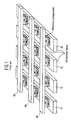
- 1 Semiconductor substrate
- 2 Via
- 3 Liner
- 4 Silicon dioxide layer
- 5 Silicon nitride layer
- 6 Silicon dioxide layer
- 7 Silicon nitride layer
- 8 Photoresist mask
- 9 Liner
- 10 Contact-making lines
- 11 Memory component
- 12 Silicon dioxide layer
- 13 Photoresist mask
- 14 Silicon nitride layer
- 15 Silicon nitride spacer
- 16 Silicon nitride layer
- 17 Silicon dioxide layer
- 18 Photoresist mask
- 19 Liner
- 20 Second contact-making lines
- 21 Photoresist mask
- 22 Silicon nitride layer
- 23 Silicon oxide layer
- 24 Photoresist mask
- 25 Silicon nitride layer
- 26 Silicon dioxide layer
- 27 Photoresist mask
- 28 Liner
- 29 Second contact-making lines
- 30 Silicon dioxide spacer
- 31 Silicon nitride layer
- 32 Silicon oxide layer
- 33 Photoresist mask
- 34 Liner
- 35 Second contact-making lines
Claims (8)
Applications Claiming Priority (3)
| Application Number | Priority Date | Filing Date | Title |
|---|---|---|---|
| DE10043159.3 | 2000-09-01 | ||
| DE10043159A DE10043159A1 (en) | 2000-09-01 | 2000-09-01 | Memory cell arrangement and method for its production |
| PCT/EP2001/009901 WO2002019338A1 (en) | 2000-09-01 | 2001-08-28 | Memory cell arrangement and method for the production thereof |
Publications (2)
| Publication Number | Publication Date |
|---|---|
| US20040004884A1 US20040004884A1 (en) | 2004-01-08 |
| US6943393B2 true US6943393B2 (en) | 2005-09-13 |
Family
ID=7654680
Family Applications (1)
| Application Number | Title | Priority Date | Filing Date |
|---|---|---|---|
| US10/343,844 Expired - Fee Related US6943393B2 (en) | 2000-09-01 | 2001-08-28 | Memory cell arrangement and method of fabricating it |
Country Status (8)
| Country | Link |
|---|---|
| US (1) | US6943393B2 (en) |
| EP (1) | EP1314165B1 (en) |
| JP (1) | JP2004508701A (en) |
| KR (1) | KR100524269B1 (en) |
| CN (1) | CN100359597C (en) |
| DE (2) | DE10043159A1 (en) |
| TW (1) | TW525287B (en) |
| WO (1) | WO2002019338A1 (en) |
Cited By (1)
| Publication number | Priority date | Publication date | Assignee | Title |
|---|---|---|---|---|
| US20090146242A1 (en) * | 2007-12-06 | 2009-06-11 | International Business Machines Corporation | Metal ion transistor and related methods |
Families Citing this family (12)
| Publication number | Priority date | Publication date | Assignee | Title |
|---|---|---|---|---|
| DE10124366A1 (en) * | 2001-05-18 | 2002-11-28 | Infineon Technologies Ag | Production of a semiconductor memory cell has spacer elements formed by depositing a material region for a first passivating region and subsequently polishing with a stop on a common level of storage elements or a protective layer |
| US6812040B2 (en) | 2002-03-12 | 2004-11-02 | Freescale Semiconductor, Inc. | Method of fabricating a self-aligned via contact for a magnetic memory element |
| US6740588B1 (en) * | 2002-03-29 | 2004-05-25 | Silicon Magnetic Systems | Smooth metal semiconductor surface and method for making the same |
| US6815248B2 (en) * | 2002-04-18 | 2004-11-09 | Infineon Technologies Ag | Material combinations for tunnel junction cap layer, tunnel junction hard mask and tunnel junction stack seed layer in MRAM processing |
| US6783994B2 (en) | 2002-04-26 | 2004-08-31 | Freescale Semiconductor, Inc. | Method of fabricating a self-aligned magnetic tunneling junction and via contact |
| US6635546B1 (en) * | 2002-05-16 | 2003-10-21 | Infineon Technologies Ag | Method and manufacturing MRAM offset cells in a damascene structure |
| US6743642B2 (en) * | 2002-11-06 | 2004-06-01 | International Business Machines Corporation | Bilayer CMP process to improve surface roughness of magnetic stack in MRAM technology |
| US6784091B1 (en) * | 2003-06-05 | 2004-08-31 | International Business Machines Corporation | Maskless array protection process flow for forming interconnect vias in magnetic random access memory devices |
| US7083990B1 (en) * | 2005-01-28 | 2006-08-01 | Infineon Technologies Ag | Method of fabricating MRAM cells |
| US7399646B2 (en) * | 2005-08-23 | 2008-07-15 | International Business Machines Corporation | Magnetic devices and techniques for formation thereof |
| US20080173975A1 (en) * | 2007-01-22 | 2008-07-24 | International Business Machines Corporation | Programmable resistor, switch or vertical memory cell |
| US9780301B1 (en) * | 2016-04-15 | 2017-10-03 | Taiwan Semiconductor Manufacturing Company Ltd. | Method for manufacturing mixed-dimension and void-free MRAM structure |
Citations (7)
| Publication number | Priority date | Publication date | Assignee | Title |
|---|---|---|---|---|
| US5756366A (en) * | 1995-12-21 | 1998-05-26 | Honeywell Inc. | Magnetic hardening of bit edges of magnetoresistive RAM |
| DE19744095A1 (en) | 1997-10-06 | 1999-04-15 | Siemens Ag | Memory cell array has stacked layer magnetoresistive effect layer memory elements |
| US5940319A (en) | 1998-08-31 | 1999-08-17 | Motorola, Inc. | Magnetic random access memory and fabricating method thereof |
| WO2000031809A1 (en) | 1998-11-19 | 2000-06-02 | Infineon Technologies Ag | Magnetoresistive element and utilisation thereof as a storage element in a storage cell array |
| WO2000038191A1 (en) | 1998-12-21 | 2000-06-29 | Motorola Inc. | Method of fabricating a magnetic random access memory |
| WO2000052701A1 (en) | 1999-02-26 | 2000-09-08 | Infineon Technologies Ag | Storage cell arrangement and method for producing the same |
| EP1054449A2 (en) | 1999-05-17 | 2000-11-22 | Motorola, Inc. | Magnetic random access memory and fabricating method thereof |
-
2000
- 2000-09-01 DE DE10043159A patent/DE10043159A1/en not_active Withdrawn
-
2001
- 2001-08-28 WO PCT/EP2001/009901 patent/WO2002019338A1/en active IP Right Grant
- 2001-08-28 KR KR10-2003-7002808A patent/KR100524269B1/en not_active IP Right Cessation
- 2001-08-28 DE DE50102622T patent/DE50102622D1/en not_active Expired - Lifetime
- 2001-08-28 CN CNB018150446A patent/CN100359597C/en not_active Expired - Fee Related
- 2001-08-28 US US10/343,844 patent/US6943393B2/en not_active Expired - Fee Related
- 2001-08-28 TW TW090121233A patent/TW525287B/en not_active IP Right Cessation
- 2001-08-28 JP JP2002524151A patent/JP2004508701A/en not_active Ceased
- 2001-08-28 EP EP01962977A patent/EP1314165B1/en not_active Expired - Lifetime
Patent Citations (8)
| Publication number | Priority date | Publication date | Assignee | Title |
|---|---|---|---|---|
| US5756366A (en) * | 1995-12-21 | 1998-05-26 | Honeywell Inc. | Magnetic hardening of bit edges of magnetoresistive RAM |
| DE19744095A1 (en) | 1997-10-06 | 1999-04-15 | Siemens Ag | Memory cell array has stacked layer magnetoresistive effect layer memory elements |
| US5940319A (en) | 1998-08-31 | 1999-08-17 | Motorola, Inc. | Magnetic random access memory and fabricating method thereof |
| WO2000031809A1 (en) | 1998-11-19 | 2000-06-02 | Infineon Technologies Ag | Magnetoresistive element and utilisation thereof as a storage element in a storage cell array |
| WO2000038191A1 (en) | 1998-12-21 | 2000-06-29 | Motorola Inc. | Method of fabricating a magnetic random access memory |
| US6153443A (en) * | 1998-12-21 | 2000-11-28 | Motorola, Inc. | Method of fabricating a magnetic random access memory |
| WO2000052701A1 (en) | 1999-02-26 | 2000-09-08 | Infineon Technologies Ag | Storage cell arrangement and method for producing the same |
| EP1054449A2 (en) | 1999-05-17 | 2000-11-22 | Motorola, Inc. | Magnetic random access memory and fabricating method thereof |
Non-Patent Citations (1)
| Title |
|---|
| Hu, Y.Z. et al., "Chemical-Mechanical Polishing as an Enabling Technology for Giant Magnetoresistance Devices", Thin Solid Films, 308-309, pp. 555-561; 1997. |
Cited By (4)
| Publication number | Priority date | Publication date | Assignee | Title |
|---|---|---|---|---|
| US20090146242A1 (en) * | 2007-12-06 | 2009-06-11 | International Business Machines Corporation | Metal ion transistor and related methods |
| US20100184280A1 (en) * | 2007-12-06 | 2010-07-22 | Fen Chen | Method of forming metal ion transistor |
| US7859025B2 (en) | 2007-12-06 | 2010-12-28 | International Business Machines Corporation | Metal ion transistor |
| US7998828B2 (en) | 2007-12-06 | 2011-08-16 | International Business Machines Corporation | Method of forming metal ion transistor |
Also Published As
| Publication number | Publication date |
|---|---|
| KR100524269B1 (en) | 2005-10-28 |
| KR20030064389A (en) | 2003-07-31 |
| TW525287B (en) | 2003-03-21 |
| CN1451164A (en) | 2003-10-22 |
| US20040004884A1 (en) | 2004-01-08 |
| DE50102622D1 (en) | 2004-07-22 |
| DE10043159A1 (en) | 2002-03-21 |
| JP2004508701A (en) | 2004-03-18 |
| CN100359597C (en) | 2008-01-02 |
| EP1314165B1 (en) | 2004-06-16 |
| WO2002019338A1 (en) | 2002-03-07 |
| EP1314165A1 (en) | 2003-05-28 |
Similar Documents
| Publication | Publication Date | Title |
|---|---|---|
| US6890770B2 (en) | Magnetoresistive random access memory device structures and methods for fabricating the same | |
| US6785159B2 (en) | Combination etch stop and in situ resistor in a magnetoresistive memory and methods for fabricating same | |
| US7402879B2 (en) | Layered magnetic structures having improved surface planarity for bit material deposition | |
| US7183130B2 (en) | Magnetic random access memory and method of fabricating thereof | |
| US6783999B1 (en) | Subtractive stud formation for MRAM manufacturing | |
| US6627913B2 (en) | Insulation of an MRAM device through a self-aligned spacer | |
| US7144744B2 (en) | Magnetoresistive random access memory device structures and methods for fabricating the same | |
| CN110970550A (en) | Magnetoresistive element and method for manufacturing the same | |
| US6943393B2 (en) | Memory cell arrangement and method of fabricating it | |
| US20210013396A1 (en) | Semiconductor structure and method for forming the same | |
| US20030117866A1 (en) | Recessed magnetic storage element and method of formation | |
| CN114447023A (en) | Semiconductor element and manufacturing method thereof | |
| US20050270830A1 (en) | Integrated circuit structure formed by damascene process | |
| JP2004319725A (en) | Magnetic random access memory device | |
| US11950513B2 (en) | Semiconductor device and method for fabricating the same | |
| CN113809117A (en) | Semiconductor element and manufacturing method thereof | |
| US11887643B2 (en) | Integrated magnetic shield for MRAM arrays | |
| US20240114803A1 (en) | Magnetoresistive random access memory and method for fabricating the same | |
| US20230363287A1 (en) | Method for manufacturing memory device | |
| CN115377283A (en) | Magnetoresistive random access memory | |
| CN116761497A (en) | Bottom needle-punched spin orbit torque magnetic memory and manufacturing method thereof | |
| CN116156995A (en) | Semiconductor structure and manufacturing method thereof | |
| CN115915904A (en) | Semiconductor element and manufacturing method thereof | |
| CN114335331A (en) | Semiconductor element and manufacturing method thereof | |
| CN116867349A (en) | Semiconductor element and manufacturing method thereof |
Legal Events
| Date | Code | Title | Description |
|---|---|---|---|
| AS | Assignment |
Owner name: INFINEON TECHNOLOGIES AG, GERMANY Free format text: ASSIGNMENT OF ASSIGNORS INTEREST;ASSIGNORS:MIETHANER, STEFAN;SCHWARZL, SIEGFRIED;SAENGER, ANNETTE;REEL/FRAME:014343/0700;SIGNING DATES FROM 20030224 TO 20030311 |
|
| FEPP | Fee payment procedure |
Free format text: PAYOR NUMBER ASSIGNED (ORIGINAL EVENT CODE: ASPN); ENTITY STATUS OF PATENT OWNER: LARGE ENTITY |
|
| REMI | Maintenance fee reminder mailed | ||
| FPAY | Fee payment |
Year of fee payment: 4 |
|
| SULP | Surcharge for late payment | ||
| AS | Assignment |
Owner name: QIMONDA AG,GERMANY Free format text: ASSIGNMENT OF ASSIGNORS INTEREST;ASSIGNOR:INFINEON TECHNOLOGIES AG;REEL/FRAME:023768/0001 Effective date: 20060425 Owner name: QIMONDA AG, GERMANY Free format text: ASSIGNMENT OF ASSIGNORS INTEREST;ASSIGNOR:INFINEON TECHNOLOGIES AG;REEL/FRAME:023768/0001 Effective date: 20060425 |
|
| FPAY | Fee payment |
Year of fee payment: 8 |
|
| AS | Assignment |
Owner name: INFINEON TECHNOLOGIES AG, GERMANY Free format text: ASSIGNMENT OF ASSIGNORS INTEREST;ASSIGNOR:QIMONDA AG;REEL/FRAME:035623/0001 Effective date: 20141009 |
|
| AS | Assignment |
Owner name: POLARIS INNOVATIONS LIMITED, IRELAND Free format text: ASSIGNMENT OF ASSIGNORS INTEREST;ASSIGNOR:INFINEON TECHNOLOGIES AG;REEL/FRAME:036615/0885 Effective date: 20150708 |
|
| REMI | Maintenance fee reminder mailed | ||
| LAPS | Lapse for failure to pay maintenance fees |
Free format text: PATENT EXPIRED FOR FAILURE TO PAY MAINTENANCE FEES (ORIGINAL EVENT CODE: EXP.) |
|
| STCH | Information on status: patent discontinuation |
Free format text: PATENT EXPIRED DUE TO NONPAYMENT OF MAINTENANCE FEES UNDER 37 CFR 1.362 |
|
| FP | Lapsed due to failure to pay maintenance fee |
Effective date: 20170913 |