US6927884B2 - Solid-state image sensing device - Google Patents
Solid-state image sensing device Download PDFInfo
- Publication number
- US6927884B2 US6927884B2 US09/922,763 US92276301A US6927884B2 US 6927884 B2 US6927884 B2 US 6927884B2 US 92276301 A US92276301 A US 92276301A US 6927884 B2 US6927884 B2 US 6927884B2
- Authority
- US
- United States
- Prior art keywords
- mos transistor
- electrode
- transistor
- amount
- solid
- Prior art date
- Legal status (The legal status is an assumption and is not a legal conclusion. Google has not performed a legal analysis and makes no representation as to the accuracy of the status listed.)
- Expired - Lifetime, expires
Links
- 239000003990 capacitor Substances 0.000 claims description 115
- 238000005070 sampling Methods 0.000 claims description 7
- 239000011159 matrix material Substances 0.000 claims description 5
- 238000006243 chemical reaction Methods 0.000 description 71
- 238000010586 diagram Methods 0.000 description 57
- 230000015654 memory Effects 0.000 description 34
- 238000002360 preparation method Methods 0.000 description 5
- 238000009792 diffusion process Methods 0.000 description 4
- 230000000694 effects Effects 0.000 description 4
- 238000005215 recombination Methods 0.000 description 4
- 230000006798 recombination Effects 0.000 description 4
- 230000006870 function Effects 0.000 description 3
- 230000003287 optical effect Effects 0.000 description 3
- 239000000758 substrate Substances 0.000 description 3
- 230000007704 transition Effects 0.000 description 3
- 238000004364 calculation method Methods 0.000 description 2
- 230000010354 integration Effects 0.000 description 2
- 229910021420 polycrystalline silicon Inorganic materials 0.000 description 2
- 229920005591 polysilicon Polymers 0.000 description 2
- 239000004065 semiconductor Substances 0.000 description 2
- 230000035945 sensitivity Effects 0.000 description 2
- 206010047571 Visual impairment Diseases 0.000 description 1
- 230000003321 amplification Effects 0.000 description 1
- 238000004519 manufacturing process Methods 0.000 description 1
- 238000000034 method Methods 0.000 description 1
- 238000003199 nucleic acid amplification method Methods 0.000 description 1
- 238000005036 potential barrier Methods 0.000 description 1
- 239000007787 solid Substances 0.000 description 1
Images


Classifications
-
- H—ELECTRICITY
- H01—ELECTRIC ELEMENTS
- H01L—SEMICONDUCTOR DEVICES NOT COVERED BY CLASS H10
- H01L27/00—Devices consisting of a plurality of semiconductor or other solid-state components formed in or on a common substrate
- H01L27/14—Devices consisting of a plurality of semiconductor or other solid-state components formed in or on a common substrate including semiconductor components sensitive to infrared radiation, light, electromagnetic radiation of shorter wavelength or corpuscular radiation and specially adapted either for the conversion of the energy of such radiation into electrical energy or for the control of electrical energy by such radiation
- H01L27/144—Devices controlled by radiation
- H01L27/146—Imager structures
- H01L27/14601—Structural or functional details thereof
- H01L27/14609—Pixel-elements with integrated switching, control, storage or amplification elements
-
- H—ELECTRICITY
- H01—ELECTRIC ELEMENTS
- H01L—SEMICONDUCTOR DEVICES NOT COVERED BY CLASS H10
- H01L27/00—Devices consisting of a plurality of semiconductor or other solid-state components formed in or on a common substrate
- H01L27/14—Devices consisting of a plurality of semiconductor or other solid-state components formed in or on a common substrate including semiconductor components sensitive to infrared radiation, light, electromagnetic radiation of shorter wavelength or corpuscular radiation and specially adapted either for the conversion of the energy of such radiation into electrical energy or for the control of electrical energy by such radiation
- H01L27/144—Devices controlled by radiation
- H01L27/146—Imager structures
- H01L27/14643—Photodiode arrays; MOS imagers
-
- H—ELECTRICITY
- H04—ELECTRIC COMMUNICATION TECHNIQUE
- H04N—PICTORIAL COMMUNICATION, e.g. TELEVISION
- H04N25/00—Circuitry of solid-state image sensors [SSIS]; Control thereof
- H04N25/50—Control of the SSIS exposure
- H04N25/57—Control of the dynamic range
- H04N25/571—Control of the dynamic range involving a non-linear response
- H04N25/573—Control of the dynamic range involving a non-linear response the logarithmic type
Definitions
- the present invention relates to a solid-state image-sensing device that is switchable between a first state in which it outputs an electric signal that is linearly proportional to the amount of incident light and a second state in which it outputs an electric signal that is natural-logarithmically proportional to the amount of incident light.
- CCD-type image-sensing devices transfer electric charge while accumulating it in potential wells.
- MOS-type image-sensing devices read out electric charge accumulated in the pn junction capacitance of photodiodes through MOS transistors.
- these conventional solid-state image-sensing devices yield outputs that are proportional to the amount of electric charge generated, and thus have the disadvantage of narrow dynamic ranges.
- a solid-state image-sensing device that is provided with a photosensitive means that produces a photocurrent commensurate with the amount of incident light, a MOS transistor to which the photocurrent is fed, and a bias means that biases the MOS transistor in such a way that a subthreshold current flows therethrough.
- This solid-state image-sensing device outputs an electric signal that is natural-logarithmically proportional to the amount of incident light.
- This type of solid-state image-sensing device has a wide dynamic range, but has the disadvantages of unsatisfactory characteristics in low-brightness condition and an insufficient SIN (signal-to-noise) ratio.
- an optical sensor circuit has also been proposed that is provided with a photosensitive means that produces a photocurrent commensurate with the amount of incident light and a MOS transistor to which the photocurrent is fed; in addition, this optical sensor circuit is so configured as to be switchable between a first state in which it yields an output linearly proportional to the photocurrent and a second state in which it yields an output natural-logarithmically proportional to the photocurrent (U.S. Pat. No. 5,861,621).
- An object of the present invention is to provide a novel and effective solid-state image-sensing device that can be switched between logarithmic conversion and linear conversion automatically according to the amount of light incident on the photoelectric conversion portion thereof.
- Another object of the present invention is to provide a solid-state image-sensing device that has a plurality of pixels and in which the switching point between linear conversion and logarithmic conversion is substantially identical in all pixels.
- a solid-state image-sensing device with: a photosensitive element that produces an electric signal commensurate with the amount of light incident thereon; a transistor of which the first electrode and the control electrode are connected to one electrode of the photosensitive element; and a resetting portion for resetting the transistor by feeding a predetermined pulse signal to the second electrode of the transistor.
- the resetting portion resets the transistor in such a way as to inhibit the transistor from operating in a subthreshold region when the amount of light incident on the photosensitive element is below a predetermined level.
- the resetting portion resets the transistor in such a way as to, on the one hand, keep the transistor in a cut-off state when the amount of light incident on the photosensitive element is below a predetermined level so that an output linearly proportional to the amount of light incident on the photosensitive element appears at the control electrode of the transistor and, on the other hand, permit the transistor to operate in a subthreshold region when the amount of light incident on the photosensitive element is equal to or above the predetermined level so that an output logarithmically proportional to the amount of light incident on the photosensitive element appears at the control electrode of the transistor.
- FIG. 1 is a block diagram illustrating the overall configuration of a two-dimensional solid-state image-sensing device embodying the invention
- FIGS. 2A and 2B are diagrams showing a portion of FIG. 1 ;
- FIG. 3 is a circuit diagram showing an example of the configuration of each pixel in a first embodiment of the invention
- FIG. 4 is a timing chart showing the operation of each pixel in the first embodiment
- FIG. 5 is a circuit diagram showing an example of the configuration of each pixel in a second embodiment of the invention.
- FIG. 6 is a timing chart showing the operation of each pixel in the second embodiment
- FIG. 7 is a circuit diagram showing an example of the configuration of each pixel in a third embodiment of the invention.
- FIG. 8 is a circuit diagram showing an example of the configuration of each pixel in a fourth embodiment of the invention.
- FIG. 9 is a circuit diagram showing an example of the configuration of each pixel in a fifth embodiment of the invention.
- FIG. 10 is a timing chart showing the operation of each pixel in the fifth embodiment.
- FIG. 11 is a circuit diagram showing an example of the configuration of each pixel in a sixth embodiment of the invention.
- FIG. 12 is a timing chart showing the operation of each pixel in the sixth embodiment.
- FIG. 13 is a circuit diagram showing an example of the configuration of each pixel in a seventh embodiment of the invention.
- FIG. 14 is a circuit diagram showing an example of the configuration of each pixel in an eighth embodiment of the invention.
- FIG. 15 is a circuit diagram showing another example of the configuration of each pixel in a fifth embodiment of the invention.
- FIG. 16 is a circuit diagram showing another example of the configuration of each pixel in a sixth embodiment of the invention.
- FIG. 17 is a circuit diagram showing another example of the configuration of each pixel in a seventh embodiment of the invention.
- FIG. 18 is a circuit diagram showing another example of the configuration of each pixel in an eighth embodiment of the invention.
- FIG. 19 is a circuit diagram showing another example of the configuration of each pixel in a fifth embodiment of the invention.
- FIG. 20 is a circuit diagram showing another example of the configuration of each pixel in a sixth embodiment of the invention.
- FIG. 21 is a circuit diagram showing another example of the configuration of each pixel in a seventh embodiment of the invention.
- FIG. 22 is a circuit diagram showing another example of the configuration of each pixel in an eighth embodiment of the invention.
- FIG. 23 is a circuit diagram showing an example of the configuration of each pixel in a ninth embodiment of the invention.
- FIG. 24 is a timing chart showing the operation of each pixel in the ninth embodiment.
- FIGS. 25A to 25 F are diagrams showing the structure of the pixel shown in FIG. 23 and the potential relationship observed therein;
- FIG. 26 is a circuit diagram showing an example of the configuration of each pixel in a tenth embodiment of the invention.
- FIG. 27 is a timing chart showing the operation of each pixel in the tenth embodiment
- FIG. 28 is a circuit diagram showing an example of the configuration of each pixel in an eleventh embodiment of the invention.
- FIG. 29 is a block diagram illustrating the overall configuration of a two-dimensional solid-state image-sensing device embodying the invention, in a case where P-channel MOS transistors are used as active elements in each pixel;
- FIGS. 30A and 30B are diagrams showing a portion of FIG. 29 ;
- FIG. 31 is a circuit diagram showing an example of the configuration of each pixel in a twelfth embodiment of the invention.
- FIG. 32 is a circuit diagram showing an example of the configuration of each pixel in a thirteenth embodiment of the invention.
- FIG. 33 is a circuit diagram showing an example of the configuration of each pixel in a fourteenth embodiment of the invention.
- FIG. 34 is a circuit diagram showing an example of the configuration of each pixel in a fifteenth embodiment of the invention.
- FIG. 35 is a circuit diagram showing an example of the configuration of each pixel in a sixteenth embodiment of the invention.
- FIG. 36 is a circuit diagram showing an example of the configuration of each pixel in a seventeenth embodiment of the invention.
- FIG. 37 is a circuit diagram showing an example of the configuration of each pixel in an eighteenth embodiment of the invention.
- FIG. 38 is a circuit diagram showing an example of the configuration of each pixel in a nineteenth embodiment of the invention.
- FIG. 39 is a circuit diagram showing another example of the configuration of each pixel in a sixteenth embodiment of the invention.
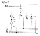
- FIG. 40 is a circuit diagram showing another example of the configuration of each pixel in a seventeenth embodiment of the invention.
- FIG. 41 is a circuit diagram showing another example of the configuration of each pixel in an eighteenth embodiment of the invention.
- FIG. 42 is a circuit diagram showing another example of the configuration of each pixel in a nineteenth embodiment of the invention.
- FIG. 43 is a circuit diagram showing another example of the configuration of each pixel in a sixteenth embodiment of the invention.
- FIG. 44 is a circuit diagram showing another example of the configuration of each pixel in a seventeenth embodiment of the invention.
- FIG. 45 is a circuit diagram showing another example of the configuration of each pixel in an eighteenth embodiment of the invention.
- FIG. 46 is a circuit diagram showing another example of the configuration of each pixel in a nineteenth embodiment of the invention.
- FIG. 47 is a circuit diagram showing an example of the configuration of each pixel in a twentieth embodiment of the invention.
- FIG. 48 is a circuit diagram showing an example of the configuration of each pixel in a twenty-first embodiment of the invention.
- FIG. 49 is a circuit diagram showing an example of the configuration of each pixel in a twenty-second embodiment of the invention.
- FIG. 50 is a block diagram showing the internal configuration of an image input apparatus incorporating the solid-state image-sensing device of one of the embodiments of the invention.
- FIG. 1 schematically shows the configuration of a portion of a two-dimensional MOS-type solid-state image-sensing device embodying the invention.
- reference symbols G 11 to Gmn represent pixels arranged in rows and columns (in a matrix).
- Reference numeral 2 represents a vertical scanning circuit, which scans rows (lines) 4 - 1 , 4 - 2 , . . . , 4 - n sequentially.
- Reference numeral 3 represents a horizontal scanning circuit, which reads out photoelectric conversion signals, which are delivered from the pixels to output signal lines 6 - 1 , 6 - 2 , . . . , 6 - m , sequentially pixel by pixel in the horizontal direction.
- Reference numeral 5 represents a power line.
- the individual pixels are connected not only to the lines 4 - 1 , 4 - 2 , . . . , 4 - n , the output signal lines 6 - 1 , 6 - 2 , . . . , 6 - m , and the power line 5 mentioned above, but also to other lines (for example, clock lines and bias supply lines); however, these other lines are omitted in FIG. 1 .
- the MOS transistor Q 1 has its gate connected to a direct-current voltage line 7 , has its drain connected to the output signal line 6 - 1 , and has its source connected to a line 8 of a direct-current voltage VPSA.
- the MOS transistor Q 2 has its drain connected to the output signal line 6 - 1 , has its source connected to a signal line 9 serving as a final destination line, and has its gate connected to the horizontal scanning circuit 3 .
- the pixels G 11 to Gmn are each provided with an N-channel MOS transistor Ta that outputs a signal based on the photoelectric charge that has been generated therein.
- This MOS transistor Ta and the MOS transistor Q 1 described above are interconnected as shown in FIG. 2 A.
- the MOS transistor Ta corresponds to the MOS transistor T 4 in the second to fourth, sixth to eighth, tenth, and eleventh embodiments, and to the MOS transistor T 2 in the first, fifth, and ninth embodiments.
- the direct-current a voltage VPSA connected to the source of the MOS transistor Q 1 and a direct-current voltage VPDA connected to the drain of the MOS transistor Ta fulfill the relation VPDA>VPSA, where VPSA equals, for example, the ground voltage.
- the upper-stage MOS transistor Ta receives a signal at its gate
- the lower-stage MOS transistor Q 1 receives a direct-current voltage DC at its gate all the time.
- the lower-stage MOS transistor Q 1 is equivalent to a resistor or constant-current source, and thus the circuit shown in FIG. 2A acts as an amplifier circuit of a source follower type. In this case, it can safely be said that the amplification performed by the MOS transistor Ta yields a current as its output.
- the MOS transistor Q 2 is controlled by the horizontal scanning circuit 3 so as to act as a switching device.
- each pixel is further provided with an N-channel MOS transistor T 3 that acts as a switch.
- the circuit shown in FIG. 2A has a configuration as shown in FIG. 2 B.
- the MOS transistor T 3 is inserted between the MOS transistor Q 1 and the MOS transistor Ta.
- the MOS transistor T 3 serves to select a row
- the MOS transistor Q 2 serves to select a column.
- the circuit configurations shown in FIGS. 1 , 2 A, and 2 B are common to all of the first to eleventh embodiments described below.
- the amplifier circuit described above amplifies the signals to a sufficiently high level, and thereby makes them easier to process in the signal processing circuit (not shown) in the succeeding stage.
- the MOS transistor Q 1 which constitutes a load resistor in the amplifier circuit, may be provided not within each pixel, but one for each of the output signal lines 6 - 1 , 6 - 2 , . . . , 6 -m, to each of which a plurality of pixels arranged in the corresponding column are connected collectively. This helps reduce the number of load resistors or constant-current sources, and thereby reduce the area occupied by the amplifier circuit on a semiconductor chip.
- FIG. 3 is a circuit diagram showing the configuration of each pixel provided in a solid-state image-sensing device in this embodiment.
- a pn photodiode PD serves as a photosensitive portion (photoelectric conversion portion).
- the anode of this photodiode PD is connected to the gate and drain of a MOS transistor T 1 and to the gate of a MOS transistor T 2 .
- the source of the MOS transistor T 2 is connected to the drain of a MOS transistor T 3 for row selection.
- the source of the MOS transistor T 3 is connected to an output signal line 6 (this output signal line 6 corresponds to the output signal lines 6 - 1 , 6 - 2 , . . . , 6 - m shown in FIG. 1 ).
- the MOS transistors T 1 to T 3 are all N-channel MOS transistors with their back gates grounded.
- a direct-current voltage VPD is applied to the cathode of the photodiode PD and to the drain of the MOS transistor T 2 .
- a signal ⁇ VPS is fed to the source of the MOS transistor T 1 .
- a signal ⁇ V is fed to the gate of the MOS transistor T 3 .
- the signal ⁇ VPS is a binary voltage signal that takes either a level VH that makes the MOS transistor T 1 operate in a subthreshold region when the amount of incident light is above a predetermined level or a level VL that is lower than the level VH and brings the MOS transistor T 1 into a conducting state.
- This pixel configured as described above operates in the following manner.
- the signal ⁇ VPS is kept at the level VL to perform the resetting operation in this way, a high-level pulse is fed as the signal ⁇ V to the gate of the MOS transistor T 3 to read out a noise signal obtained during the resetting operation.
- the gate voltage of the MOS transistor T 1 in its reset state is fed to the gate of the MOS transistor T 2 .
- the gate voltage of the MOS transistor T 1 is current-amplified by the MOS transistor T 2 , and is then delivered through the MOS transistor T 3 to the output signal line 6 .
- the drain voltage of the MOS transistor Q 1 which is determined by the on-state resistances of the MOS transistor T 2 and the MOS transistor Q 1 ( FIG. 2 ) and the current flowing therethrough, appears as a noise signal on the output signal line 6 .
- the MOS transistor T 3 is turned off, and then the signal ⁇ VPS is turned to the level VH in preparation for an image-sensing operation that is to follow.
- a voltage linearly or natural-logarithmically proportional to the amount of incident light appears at the gates of the MOS transistors T 1 and T 2 .
- a pulse is fed as the signal ⁇ V to the gate of the MOS transistor T 3 , so that the gate voltage of the MOS transistor T 1 , which is linearly or natural-logarithmically proportional to the amount of incident light, is current-amplified by the MOS transistor T 2 , and is then delivered through the MOS transistor T 3 to the output signal line 6 .
- the drain voltage of the MOS transistor Q 1 which is determined by the on-state resistances of the MOS transistor T 2 and the MOS transistor Q 1 and the current flowing therethrough, appears as an image signal on the output signal line 6 .
- the threshold voltage of the MOS transistor T 1 varies from one pixel to another, and therefore, when the signal ⁇ VPS is at the level VH, the voltage at which a switching from linear conversion to logarithmic conversion takes place is VH+V TH ⁇ K (where V TH represents the threshold voltage of the MOS transistor T 1 and K represents a constant).
- V TH represents the threshold voltage of the MOS transistor T 1
- K represents a constant
- the amount of photoelectric charge that flows into the MOS transistor T 1 before the gate voltage of the MOS transistor T 1 reaches the voltage at which a switching to logarithmic conversion takes place is equal in all the pixels.
- the amount of electric charge that is generated in the photodiode PD when a switching to logarithmic conversion takes place is equal in all the pixels, and therefore the amount of light incident on the photodiode PD when a switching to logarithmic conversion takes place is equal in all the pixels. That is, in all the pixels, the brightness of the subject at which a switching from linear conversion to logarithmic conversion takes place is equal. In this way, it is possible to reduce the effect of variations in the threshold voltage of the MOS transistor T 1 among the individual pixels on their switching from one type of conversion to another.
- the level VL of the signal ⁇ VPS in the resetting operation By varying the level VL of the signal ⁇ VPS in the resetting operation, it is possible to vary the range in which the gate voltage VG of the MOS transistor T 1 is allowed to vary in linear conversion. Thus, by varying the level VL of the signal ⁇ VPS in the resetting operation, it is possible to set the switching point, which corresponds to the brightness of the subject at which a switching from linear conversion to logarithmic conversion takes place in the individual pixels, at the desired level.
- the noise signals from the individual pixels are fed out by way of the signal line 9 shown in FIG. 1 , serially from one pixel after another, so as to be stored as pixel-by-pixel noise signals in a memory provided in the succeeding circuit. Then, the image signals from the individual pixels are corrected with the noise signals thus stored. In this way, it is possible to eliminate, from the image signals, components resulting from variations in characteristics among the individual pixels. A practical example of how this correction is achieved is shown in FIG. 50 and will be described later. Alternatively, similar correction may be realized by providing memories, such as line memories, within the pixels.
- FIG. 5 is a circuit diagram showing the configuration of each pixel provided in a solid-state image-sensing device in this embodiment.
- circuit elements, signal lines, etc. as serve the same purposes as in the pixel shown in FIG. 3 are identified with the same reference numerals or symbols, and their detailed explanations will not be repeated.
- the pixel of this embodiment is obtained by additionally providing, in the pixel of the first embodiment (FIG. 3 ), a capacitor C 1 that has one end connected to the source of the MOS transistor T 2 , and a MOS transistor T 4 that has its gate connected to the source of the MOS transistor T 2 .
- the MOS transistor T 4 has its source connected to the drain of the MOS transistor T 3 , and receives the direct-current voltage VPD at its drain.
- a signal ⁇ D is fed to the drain of the MOS transistor T 2 , and a direct-current voltage VPS is applied to the other end of the capacitor Cl.
- the MOS transistor T 4 like the MOS transistors T 1 to T 3 , is an N-channel MOS transistor with its back gate grounded. This pixel configured as described above operates in the following manner.
- the gate voltage of the MOS transistor T 1 in its reset state is fed to the gate of the MOS transistor T 2 , so that a current commensurate with the gate voltage of the MOS transistor T 1 flows through the MOS transistor T 2 , as its drain current, to the capacitor C 1 , and thus charges the capacitor C 1 .
- the voltage at the node between the capacitor C 1 and the source of the MOS transistor T 2 is now commensurate with the gate voltage of the MOS transistor T 1 in its reset state.
- a high-level pulse is fed as the signal ⁇ V to the gate of the MOS transistor T 3 to read out a noise signal obtained during the resetting operation.
- the voltage at the node between the capacitor C 1 and the source of the MOS transistor T 2 is fed to the MOS transistor T 4 , which current-amplifies it to produce an output current, which is then delivered through the MOS transistor T 3 to the output signal line 6 .
- a low-level signal is fed as the signal ⁇ D to the drain of the MOS transistor T 2 again to reset the voltage at the node between the capacitor C 1 and the source of the MOS transistor T 2 .
- the signal ⁇ VPS is turned to the level VH in preparation for an image-sensing operation.
- a high-level pulse is fed as the signal ⁇ V to the gate of the MOS transistor T 3 to read out an image signal obtained during the image-sensing operation.
- the voltage at the node between the capacitor C 1 and the source of the MOS transistor T 2 is fed to the MOS transistor T 4 , which current-amplifies it to produce an output current, which is then delivered through the MOS transistor T 3 to the output signal line 6 .
- the output current thus delivered to the output signal line 6 is linearly or natural-logarithmically proportional to the integral of the amount of incident light.
- the MOS transistor T 2 receives at its gate, if the brightness is below a predetermined level, a voltage linearly proportional to the integral of the amount of incident light or, if the brightness is equal to or above the predetermined level, a voltage natural-logarithmically proportional to the integral of the amount of incident light.
- the use of the capacitor C 1 makes it possible to integrate the output signal before it is fed out.
- the capacitor C 1 absorbs and eliminates, from the output signal, undesirable components such as fluctuation originating from a light source and high-frequency noise. Thus, it is possible to obtain output signals with a satisfactory S/N ratio.
- the noise signals from the individual pixels are fed out by way of the signal line 9 shown in FIG. 1 , serially from one pixel after another, so as to be stored as pixel-by-pixel noise signals in a memory provided in the succeeding circuit. Then, the image signals from the individual pixels are corrected with the noise signals thus stored. In this way, it is possible to eliminate, from the image signals, components resulting from variations in characteristics among the individual pixels. A practical example of how this correction is achieved is shown in FIG. 50 and will be described later. Alternatively, similar correction may be realized by providing memories, such as line memories, within the pixels.
- FIG. 7 is a circuit diagram showing the configuration of each pixel provided in a solid-state image-sensing device in this embodiment.
- circuit elements, signal lines, etc. as serve the same purposes as in the pixel shown in FIG. 5 are identified with the same reference numerals or symbols, and their detailed explanations will not be repeated.
- the pixel of this embodiment is obtained by additionally providing, in the pixel of the second embodiment (FIG. 5 ), a MOS transistor T 5 that has its drain connected to the node between the source of the MOS transistor T 2 and the capacitor C 1 , a capacitor C 2 that has one end connected to the source of the MOS transistor T 5 , and a MOS transistor T 6 that has its drain connected to the source of the MOS transistor T 5 .
- a direct-current voltage VRS is applied to the source of the MOS transistor T 6 , and a signal ⁇ RS is fed to the gate of the MOS transistor T 6 .
- a signal ⁇ S is fed to the gate of the MOS transistor T 5 , and the voltage VPS is fed to the other end of the capacitor C 2 .
- the MOS transistors T 5 and T 6 like the MOS transistors T 1 to T 4 , are N-channel MOS transistors with their back gates grounded. This pixel configured as described above operates in the following manner.
- the gate voltage of the MOS transistor T 1 in its reset state is fed to the gate of the MOS transistor T 2 , so that a current commensurate with the gate voltage of the MOS transistor T 1 flows through the MOS transistor T 2 , as its drain current, to the capacitor C 1 , and thus charges the capacitor C 1 .
- the voltage at the node between the capacitor C 1 and the source of the MOS transistor T 2 is now commensurate with the gate voltage of the MOS transistor T 1 in its reset state.
- the signal ⁇ VPS is turned to the level VH in preparation for an image-sensing operation that is to follow.
- the manipulation of the signals ⁇ D and ⁇ VPS here is performed simultaneously for all the pixels G 11 to Gmn shown in FIG. 1 .
- a high-level pulse is fed as the signal ⁇ S to the gate of the MOS transistor T 5 to bring this MOS transistor T 5 into a conducting state, so that the voltage at the node between the capacitor C 1 and the source of the MOS transistor T 2 is sampled by the capacitor C 2 .
- the voltage at the node between the capacitor C 2 and the gate of the MOS transistor T 4 is now linearly or natural-logarithmically proportional to the integral of the amount of incident light.
- the operations performed after the image-sensing operation is started until the signal ⁇ S is fed in are performed simultaneously for all the pixels G 11 to Gmn shown in FIG. 1 .
- the MOS transistor T 2 receives at its gate, if the brightness is below a predetermined level, a voltage linearly proportional to the amount of incident light or, if the brightness is equal to or above the predetermined level, a voltage natural-logarithmically proportional to the amount of incident light.
- a high-level pulse is fed as the signal ⁇ V to the gate of the MOS transistor T 3 to read out an image signal obtained during the image-sensing operation.
- the voltage at the node between the capacitor C 2 and the gate of the MOS transistor T 4 is fed to the MOS transistor T 4 , which current-amplifies it to produce an output current, which is then delivered through the MOS transistor T 3 to the output signal line 6 .
- the output current thus delivered to the output signal line 6 is linearly or natural-logarithmically proportional to the integral of the amount of incident light.
- the use of the capacitor C 1 makes it possible to integrate the output signal before it is fed out.
- the capacitor C 1 absorbs and eliminates, from the output signal, undesirable components such as fluctuation originating from a light source and high-frequency noise.
- by feeding the signal ⁇ S simultaneously to all the pixels it is possible to sample, by using the capacitor C 2 , the image signals obtained through integration performed simultaneously in the individual pixels. This makes it possible to sense a fast-moving subject with no distortion in the image obtained.
- FIG. 8 is a circuit diagram showing the configuration of each pixel provided in a solid-state image-sensing device in this embodiment.
- circuit elements, signal lines, etc. as serve the same purposes as in the pixel shown in FIG. 7 are identified with the same reference numerals or symbols, and their detailed explanations will not be repeated.
- the pixel of this embodiment is obtained by omitting the MOS transistor T 2 from the pixel of the third embodiment (FIG. 7 ). Specifically, the node between the drain and gate of the MOS transistor T 1 is connected to the node between the capacitor C 1 and the drain of the MOS transistor T 5 .
- This pixel configured as described above operates in the following manner.
- the voltage at the node between the capacitor C 2 and the gate of the MOS transistor T 4 is now linearly or natural-logarithmically proportional to the amount of incident light.
- the operations performed after the image-sensing operation is started until the signal ⁇ S is fed in are performed simultaneously for all the pixels G 11 to Gmn shown in FIG. 1 .
- an output linearly proportional to the amount of incident light or an output natural-logarithmically proportional to the amount of incident light is sampled in the capacitor C 1 .
- the use of the capacitor C 1 makes it possible to integrate the output signal before it is fed out.
- the capacitor C 1 absorbs and eliminates, from the output signal, undesirable components such as fluctuation originating from a light source and high-frequency noise.
- by feeding the signal ⁇ S simultaneously to all the pixels it is possible to sample, by using the capacitor C 2 , the image signals obtained through sampling performed simultaneously in the individual pixels by using capacitor C 1 . This makes it possible to sense a fast-moving subject with no distortion in the image obtained.
- FIG. 9 is a circuit diagram showing the configuration of each pixel provided in a solid-state image-sensing device in this embodiment.
- circuit elements, signal lines, etc. as serve the same purposes as in the pixel shown in FIG. 3 are identified with the same reference numerals or symbols, and their detailed explanations will not be repeated.
- the pixel of this embodiment is obtained by additionally providing, in the pixel of the first embodiment (FIG. 3 ), a MOS transistor T 7 that is connected between the anode of the photodiode PD and the drain of the MOS transistor T 1 .
- the MOS transistor T 7 has its drain connected to the anode of the photodiode PD, has its source connected to the drain of the MOS transistor T 1 , and receives a signal ⁇ SW at its gate.
- the MOS transistor T 7 like the MOS transistors T 1 to T 3 , is an N-channel MOS transistor with its back gate grounded.
- this pixel configured as described above, in either of a resetting or image-sensing operation, by keeping a high level fed as the signal ⁇ SW to the gate of the MOS transistor T 7 so as to keep the MOS transistor T 7 on, it is possible to keep the pixel in the same state as the pixel of the first embodiment. That is, by keeping the MOS transistor T 7 on so as to keep the anode of the photodiode PD electrically connected to the drain of the MOS transistor T 1 , it is possible to switch between linear conversion and logarithmic conversion automatically according to the brightness of the subject.
- how this pixel operates when the MOS transistor T 7 is kept on is the same as described earlier in connection with the first embodiment, and therefore will not be described anew.
- the signal ⁇ VPS takes either a level Vh that is substantially equal to the direct-current voltage VPS and makes the MOS transistor T 1 operate in a subthreshold region or a level Vl that is lower than the level Vh and brings the MOS transistor T 1 into a conducting state.
- the resetting operation slows down. This slowing down is particularly remarkable when a bright subject suddenly becomes dim.
- the signal ⁇ VPS fed to the source of the MOS transistor T 1 is turned to the level Vl. Lowering the source voltage of the MOS transistor T 1 in this way increases the amount of negative electric charge that flows into the MOS transistor T 1 through its source. This prompts the recombination of the positive electric charge accumulated at the gate and drain of the MOS transistor T 1 , at the gate of the MOS transistor T 2 , and at the anode of the photodiode PD.
- the potential at the drain and sub-gate region of the MOS transistor T 1 lowers further. Then, the signal ⁇ VPS fed to the source of the MOS transistor T 1 is turned to the level Vh, so that the MOS transistor T 1 is reset to its original potential state. After the MOS transistor T 1 is reset to its original potential state in this way, a high-level pulse is fed as the signal ⁇ V to the gate of the MOS transistor T 3 to read out a noise signal obtained during the resetting operation. After the noise signal is read out in this way, the MOS transistor T 3 is turned off, and then the signal ⁇ SW is turned to a high level in preparation for an image-sensing operation that is to follow.
- the MOS transistor T 1 receives as its source voltage the level Vh as the signal ⁇ VPS, and therefore operates in a subthreshold region. As a result, a voltage natural-logarithmically proportional to the photocurrent appears at the gates of the MOS transistors T 1 and T 2 .
- the MOS transistor T 7 By turning the MOS transistor T 7 off in the resetting operation, it is possible to reset the MOS transistor T 1 without the influence of the photocurrent flowing from the photodiode PD.
- the MOS transistor T 1 operates in a subthreshold region all the time, and therefore it is possible to make the pixel perform logarithmic conversion over the entire brightness range.
- the noise signals from the individual pixels are fed out by way of the signal line 9 shown in FIG. 1 , serially from one pixel after another, so as to be stored as pixel-by-pixel noise signals in a memory provided in the succeeding circuit. Then, the image signals from the individual pixels are corrected with the noise signals thus stored. In this way, it is possible to eliminate, from the image signals, components resulting from variations in characteristics among the individual pixels. A practical example of how this correction is achieved is shown in FIG. 50 and will be described later. Alternatively, similar correction may be realized by providing memories, such as line memories, within the pixels.
- FIG. 11 is a circuit diagram showing the configuration of each pixel provided in a solid-state image-sensing device in this embodiment.
- circuit elements, signal lines, etc. as serve the same purposes as in the pixel shown in FIG. 5 are identified with the same reference numerals or symbols, and their detailed explanations will not be repeated.
- the pixel of this embodiment is obtained by additionally providing, in the pixel of the second embodiment (FIG. 5 ), a MOS transistor T 7 that is connected between the anode of the photodiode PD and the drain of the MOS transistor T 1 .
- the MOS transistor T 7 has its drain connected to the anode of the photodiode PD, has its source connected to the drain of the MOS transistor T 1 , and receives a signal ⁇ SW at its gate.
- this pixel configured as described above, as in the fifth embodiment, in either of a resetting or image-sensing operation, by keeping a high level fed as the signal ⁇ SW to the gate of the MOS transistor T 7 so as to keep the MOS transistor T 7 on, it is possible to keep the pixel in the same state as the pixel of the second embodiment. That is, by keeping the MOS transistor T 7 on so as to keep the anode of the photodiode PD electrically connected to the drain of the MOS transistor T 1 , it is possible to switch between linear conversion and logarithmic conversion automatically according to the brightness of the subject. Thus, how this pixel operates when the MOS transistor T 7 is kept on is the same as described earlier in connection with the second embodiment, and therefore will not be described anew.
- the signal ⁇ VPS takes either a level Vh that is substantially equal to the direct-current voltage VPS and makes the MOS transistor T 1 operate in a subthreshold region or a level Vl that is lower than the level Vh and brings the MOS transistor T 1 into a conducting state.
- the signal ⁇ VPS fed to the source of the MOS transistor T 1 is turned to the level Vl.
- Lowering the source voltage of the MOS transistor T 1 in this way increases the amount of negative electric charge that flows into the MOS transistor T 1 through its source. This prompts the recombination of the positive electric charge accumulated at the gate and drain of the MOS transistor T 1 , at the gate of the MOS transistor T 2 , and at the anode of the photodiode PD.
- the potential at the drain and sub-gate region of the MOS transistor Ti lowers further.
- the signal ⁇ VPS fed to the source of the MOS transistor T 1 is turned to the level Vh, so that the MOS transistor T 1 is reset to its original potential state.
- a low-level pulse is fed as the signal ⁇ D to the drain of the MOS transistor T 2 , so that the electric charge accumulated in the capacitor C 1 is discharged through the MOS transistor T 2 to the signal line of the signal ⁇ D. This initializes the voltage at the node between the capacitor C 1 and the source of the MOS transistor T 2 .
- the gate voltage of the MOS transistor T 1 in its reset state is fed to the gate of the MOS transistor T 2 , so that the drain current of the MOS transistor T 2 , which the MOS transistor T 2 produces by current-amplifying the gate voltage of the MOS transistor T 1 , flows to the capacitor C 1 , and thus charges the capacitor C 1 .
- the voltage at the node between the capacitor C 1 and the source of the MOS transistor T 2 is now commensurate with the gate voltage of the MOS transistor T 1 in its reset state.
- a high-level pulse is fed as the signal ⁇ V to the gate of the MOS transistor T 3 to read out a noise signal obtained during the resetting operation.
- the voltage at the node between the capacitor C 1 and the source of the MOS transistor T 2 is fed to the MOS transistor T 4 , which current-amplifies it to produce an output current, which is then delivered through the MOS transistor T 3 to the output signal line 6 .
- a low-level signal is fed as the signal ⁇ D to the drain of the MOS transistor T 2 again to reset the voltage at the node between the capacitor C 1 and the source of the MOS transistor T 2 .
- the signal ⁇ SW is turned to a high level in preparation for an image-sensing operation that is to follow.
- the MOS transistor T 1 receives as its source voltage the level Vh as the signal ⁇ VPS, and therefore operates in a subthreshold region. As a result, a voltage natural-logarithmically proportional to the photocurrent appears at the gates of the MOS transistors T 1 and T 2 .
- a high-level pulse is fed as the signal ⁇ V to the gate of the MOS transistor T 3 to read out an image signal obtained during the image-sensing operation.
- the voltage at the node between the capacitor C 1 and the source of the MOS transistor T 2 is fed to the MOS transistor T 4 , which current-amplifies it to produce an output current, which is then delivered through the MOS transistor T 3 to the output signal line 6 .
- the output current thus delivered to the output signal line 6 is natural-logarithmically proportional to the integral of the amount of incident light.
- the MOS transistor T 7 By turning the MOS transistor T 7 off in the resetting operation, it is possible to reset the MOS transistor T 1 without the influence of the photocurrent flowing from the photodiode PD.
- the MOS transistor T 1 operates in a subthreshold region all the time, and therefore it is possible to make the pixel perform logarithmic conversion over the entire brightness range.
- the noise signals from the individual pixels are fed out by way of the signal line 9 shown in FIG. 1 , serially from one pixel after another, so as to be stored as pixel-by-pixel noise signals in a memory provided in the succeeding circuit. Then, the image signals from the individual pixels are corrected with the noise signals thus stored. In this way, it is possible to eliminate, from the image signals, components resulting from variations in characteristics among the individual pixels. A practical example of how this correction is achieved is shown in FIG. 50 and will be described later. Alternatively, similar correction may be realized by providing memories, such as line memories, within the pixels.
- FIG. 13 is a circuit diagram showing the configuration of each pixel provided in a solid-state image-sensing device in this embodiment.
- circuit elements, signal lines, etc. as serve the same purposes as in the pixel shown in FIG. 7 are identified with the same reference numerals or symbols, and their detailed explanations will not be repeated.
- the pixel of this embodiment is obtained by additionally providing, in the pixel of the third embodiment (FIG. 7 ), a MOS transistor T 7 that is connected between the anode of the photodiode PD and the drain of the MOS transistor T 1 .
- the MOS transistor T 7 has its drain connected to the anode of the photodiode PD, has its source connected to the drain of the MOS transistor T 1 , and receives a signal ⁇ SW at its gate.
- this pixel configured as described above, as in the fifth embodiment, in either of a resetting or image-sensing operation, by keeping a high level fed as the signal ⁇ SW to the gate of the MOS transistor T 7 so as to keep the MOS transistor T 7 on, it is possible to keep the pixel in the same state as the pixel of the third embodiment. That is, by keeping the MOS transistor T 7 on so as to keep the anode of the photodiode PD electrically connected to the drain of the MOS transistor T 1 , it is possible to switch between linear conversion and logarithmic conversion automatically according to the brightness of the subject. Thus, how this pixel operates when the MOS transistor T 7 is kept on is the same as described earlier in connection with the third embodiment, and therefore will not be described anew.
- the signal ⁇ VPS takes either a level Vh that is substantially equal to the direct-current voltage VPS and makes the MOS transistor T 1 operate in a subthreshold region or a level Vl that is lower than the level Vh and brings the MOS transistor T 1 into a conducting state.
- the signal ⁇ VPS fed to the source of the MOS transistor T 1 is turned to the level Vh, so that the MOS transistor T 1 is reset to its original potential state.
- a low-level pulse is fed as the signal ⁇ D to the drain of the MOS transistor T 2 , so that the electric charge accumulated in the capacitor C 1 is discharged through the MOS transistor T 2 to the signal line of the signal ⁇ D. This initializes the voltage at the node between the capacitor C 1 and the source of the MOS transistor T 2 .
- a pulse is fed in as the signal ⁇ RS to initialize the capacitor C 2 .
- the gate voltage of the MOS transistor T 1 in its reset state is fed to the gate of the MOS transistor T 2 , so that the drain current of the MOS transistor T 2 , which the MOS transistor T 2 produces by current-amplifying the gate voltage of the MOS transistor T 1 , flows to the capacitor C 1 , and thus charges the capacitor C 1 .
- the voltage at the node between the capacitor C 1 and the source of the MOS transistor T 2 is now commensurate with the gate voltage of the MOS transistor T 1 in its reset state.
- the signal ⁇ SW is turned to a high level to start an image-sensing operation.
- the MOS transistor T 1 receives as its source voltage the level Vh as the signal ⁇ VPS, and therefore operates in a subthreshold region.
- a voltage natural-logarithmically proportional to the amount of light incident on the photodiode PD appears at the gates of the MOS transistors T 1 and T 2 .
- This voltage natural-logarithmically proportional to the amount of incident light is current-amplified by the MOS transistor T 2 , and the resulting current, i.e. the drain current of the MOS transistor T 2 , flows to the capacitor C 1 , and thus charges the capacitor C 1 .
- the voltage at the node between the capacitor C 1 and the source of the MOS transistor T 2 is now natural-logarithmically proportional to the integral of the amount of incident light.
- a high-level pulse is fed as the signal ⁇ S to the gate of the MOS transistor T 5 to bring this MOS transistor T 5 into a conducting state, so that the voltage at the node between the capacitor C 1 and the source of the MOS transistor T 2 is sampled by the capacitor C 2 .
- the voltage at the node between the capacitor C 2 and the gate of the MOS transistor T 4 is now natural-logarithmically proportional to the integral of the amount of incident light.
- a high-level pulse is fed as the signal ⁇ V to the gate of the MOS transistor T 3 to read out an image signal obtained during the image-sensing operation.
- the voltage at the node between the capacitor C 2 and the gate of the MOS transistor T 4 is fed to the MOS transistor T 4 , which current-amplifies it to produce an output current, which is then delivered through the MOS transistor T 3 to the output signal line 6 .
- the output current thus delivered to the output signal line 6 is natural-logarithmically proportional to the integral of the amount of incident light.
- the MOS transistor T 7 By turning the MOS transistor T 7 off in the resetting operation, it is possible to reset the MOS transistor T 1 without the influence of the photocurrent flowing from the photodiode PD.
- the MOS transistor T 1 operates in a subthreshold region all the time, and therefore it is possible to make the pixel perform logarithmic conversion over the entire brightness range.
- FIG. 14 is a circuit diagram showing the configuration of each pixel provided in a solid-state image-sensing device in this embodiment.
- circuit elements, signal lines, etc. as serve the same purposes as in the pixel shown in FIG. 8 are identified with the same reference numerals or symbols, and their detailed explanations will not be repeated.
- the pixel of this embodiment is obtained by additionally providing, in the pixel of the fourth embodiment (FIG. 8 ), a MOS transistor T 7 that is connected between the anode of the photodiode PD and the drain of the MOS transistor T 1 .
- the MOS transistor T 7 has its drain connected to the anode of the photodiode PD, has its source connected to the drain of the MOS transistor T 1 , and receives a signal ⁇ SW at its gate.
- this pixel configured as described above, as in the fifth embodiment, in either of a resetting or image-sensing operation, by keeping a high level fed as the signal ⁇ SW to the gate of the MOS transistor T 7 so as to keep the MOS transistor T 7 on, it is possible to keep the pixel in the same state as the pixel of the fourth embodiment. That is, by keeping the MOS transistor T 7 on so as to keep the anode of the photodiode PD electrically connected to the drain of the MOS transistor T 1 , it is possible to switch between linear conversion and logarithmic conversion automatically according to the brightness of the subject. Thus, how this pixel operates when the MOS transistor T 7 is kept on is the same as described earlier in connection with the fourth embodiment, and therefore will not be described anew.
- the signal ⁇ VPS takes either a level Vh that is substantially equal to the direct-current voltage VPS and makes the MOS transistor T 1 operate in a subthreshold region or a level Vl that is lower than the level Vh and brings the MOS transistor T 1 into a conducting state.
- the signal ⁇ VPS fed to the source of the MOS transistor T 1 is turned to the level Vh, so that the MOS transistor T 1 is reset to its original potential state.
- the signal ⁇ SW is turned to a high level to start an image-sensing operation.
- the MOS transistor T 1 receives as its source voltage the level Vh as the signal ⁇ VPS, and therefore operates in a subthreshold region.
- a voltage natural-logarithmically proportional to the amount of light incident on the photodiode PD appears at the gate of the MOS transistor T 1 .
- This voltage natural-logarithmically proportional to the amount of incident light is sampled by the capacitor C 1 .
- a high-level pulse is fed as the signal ⁇ V to the gate of the MOS transistor T 3 to read out an image signal obtained during the image-sensing operation.
- the voltage at the node between the capacitor C 2 and the gate of the MOS transistor T 4 is fed to the MOS transistor T 4 , which current-amplifies it to produce an output current, which is then delivered through the MOS transistor T 3 to the output signal line 6 .
- the output current thus delivered to the output signal line 6 is natural-logarithmically proportional to the integral of the amount of incident light.
- the MOS transistor T 7 By turning the MOS transistor T 7 off in the resetting operation, it is possible to reset the MOS transistor T 1 without the influence of the photocurrent flowing from the photodiode PD.
- the MOS transistor T 1 operates in a subthreshold region all the time, and therefore it is possible to make the pixel perform logarithmic conversion over the entire brightness range.
- the MOS transistor T 7 may be formed as a depletion-mode N-channel MOS transistor.
- the pixels of those embodiments have circuit configurations as shown in FIGS. 15 to 18 , respectively.
- all the other transistors T 1 to T 6 than the MOS transistor T 7 are formed as enhancement-mode N-channel MOS transistors.
- MOS transistors T 1 and T 7 are connected in series, and therefore the high-level voltage of the signal ⁇ SW fed to the gate of the MOS transistor T 7 is usually higher than the voltage supplied to the pixel. Thus, it is usually necessary to provide a separate power source for feeding the signal ⁇ SW to the MOS transistor T 7 .
- this MOS transistor T 7 a depletion-mode MOS transistor, it is possible to lower the high-level voltage of the signal ⁇ SW fed to the gate thereof, and thus make this high-level voltage equal to the high-level signals fed to the other MOS transistors. This is because a depletion-mode MOS transistor has a negative threshold voltage value and can thus be turned on with a lower gate voltage than an enhancement-mode MOS transistor.
- the MOS transistor T 7 may be formed as a P-channel MOS transistor.
- the pixels of those embodiments have circuit configurations as shown in FIGS. 19 to 22 , respectively.
- all the other transistors T 1 to T 6 than the MOS transistor T 7 are formed as N-channel MOS transistors.
- the MOS transistor T 7 has its source connected to the anode of the photodiode PD, and has its drain connected to the drain of the MOS transistor T 1 .
- the MOS transistor T 7 is turned on when the voltage difference between its gate and drain is greater than its threshold voltage, and is turned off when the voltage difference between its gate and drain is smaller than its threshold voltage. Accordingly, the signal ⁇ SW fed to the gate of the MOS transistor T 7 has an inverted level-shift pattern as compared with the signal ⁇ SW in the fifth to eighth embodiments. Moreover, the MOS transistor T 7 can be turned on and off without being affected by the MOS transistor T 1 that is connected in series with the drain of the MOS transistor T 7 .
- MOS transistor T 7 can be turned on and off without being affected by the MOS transistor T 1 , there is no need to provide a separate power source for feeding the signal ⁇ SW. Furthermore, these circuit configurations permit the MOS transistor T 7 to be formed as an enhancement-mode MOS transistor like all the other MOS transistors, and thus allow the MOS transistor T 7 to be produced together with the other MOS transistors in a single step. This helps simplify the manufacturing process as compared with the circuit configurations described above in which only the MOS transistor T 7 is formed as a depletion-mode MOS transistor.
- FIG. 23 is a circuit diagram showing the configuration of each pixel provided in a solid-state image-sensing device in this embodiment.
- circuit elements, signal lines, etc. as serve the same purposes as in the pixel shown in FIG. 3 are identified with the same reference numerals or symbols, and their detailed explanations will not be repeated.
- the cathode of the photodiode PD is connected to the source of a MOS transistor T 8 and to the gate of the MOS transistor T 2 .
- the source of the MOS transistor T 2 is connected to the drain of the MOS transistor T 3 for row selection.
- the source of the MOS transistor T 3 is connected to the output signal line 6 (this output signal line 6 corresponds to the output signal lines 6 - 1 , 6 - 2 , . . . , 6 - m shown in FIG. 1 ).
- the MOS transistors T 2 , T 3 , and T 8 are all N-channel MOS transistors with their back gates grounded.
- a direct-current voltage VPS is applied to the anode of the photodiode PD, and the direct-current voltage VPD is applied to the drain of the MOS transistor T 2 .
- the signal ⁇ V is fed to the gate of the MOS transistor T 3 .
- a signal ⁇ VPD is fed to the drain of the MOS transistor T 8 , and a signal ⁇ VPG is fed to the gate of the MOS transistor T 8 .
- the signal ⁇ VPG is a binary voltage signal that takes either a level Va that makes the MOS transistor T 8 operate in a subthreshold region when the amount of incident light is above a predetermined level or a level Vb that is higher than the level Va and is used to initialize the source voltage of the MOS transistor T 8 .
- the signal ⁇ VPD is a binary voltage signal that takes either a high level that is higher than the level Vb or a low level that is lower than the level Va. This pixel configured as described above operates in the following manner.
- the MOS transistor T 8 is formed, for example, by forming N-type diffusion layers 11 and 12 in a P-type semiconductor substrate (hereinafter referred to as the “P-type substrate”) 10 and then forming, on top of the channel left between those N-type diffusion layers 11 and 12 , an oxide film 13 and, further on top thereof, a polysilicon layer 14 .
- the N-type diffusion layers 11 and 12 function as the drain and the source, respectively, of the MOS transistor T 8
- the oxide film 13 and the polysilicon layer 14 function as the gate insulating film and the gate electrode, respectively, thereof.
- the region between the N-type diffusion layers 11 and 12 is called the sub-gate region.
- arrows indicate the direction in which the potential increases.
- the MOS transistor T 8 is, for example, in a potential state as indicated with solid lines in FIG. 25B , in which the source, the sub-gate region, and the drain have increasingly high potentials in this order, or in a potential state as indicated with solid and dash-dot lines in FIG. 25B , in which the sub-gate region, the source, and the drain have increasingly high potentials in this order.
- the signal ⁇ VPD when the signal ⁇ VPD is turned to a low level, electric charge is injected into the sub-gate region and source of the MOS transistor T 8 through the drain thereof, with the result that, as shown in FIG. 25C , the drain, the sub-gate region, and the source all come to have a potential that corresponds to the low level of the signal ⁇ VPD.
- the signal ⁇ VPG is at the level Va.
- the drain of the MOS transistor T 8 comes to have a potential that corresponds to the high level of the signal ⁇ VPD, and the sub-gate region and the source of the MOS transistor T 8 come to have a potential that corresponds to the level Va of the signal ⁇ VPG.
- the sub-gate region of the MOS transistor T 8 comes to have a potential that corresponds to the level Va of the signal ⁇ VPG, i.e. a potential lower than its potential in the state shown in FIG. 25 E.
- the potential at the source of the MOS transistor T 8 is now higher than the potential at the sub-gate region thereof.
- the MOS transistor T 8 operates in a subthreshold region. As a result, a voltage natural-logarithmically proportional to the amount of incident light appears at the source of the MOS transistor T 8 .
- the drain voltage of the MOS transistor Q 1 which is determined by the on-state resistances of the MOS transistor T 2 and the MOS transistor Q 1 and the current flowing therethrough, appears as an image signal on the output signal line 6 . After the image signal is read out in this way, the resetting operation described earlier is performed.
- the threshold voltage of the MOS transistor T 8 varies from one pixel to another, and therefore, when the signal ⁇ VPG is at the level Va, the voltage at which a switching from linear conversion to logarithmic conversion takes place is Va+Vx (where Vx represents the component of the voltage that results from a variation in the threshold voltage of the MOS transistor T 8 ).
- Vx represents the component of the voltage that results from a variation in the threshold voltage of the MOS transistor T 8 .
- the voltage at the source electrode of the MOS transistor T 8 is substantially equal to Vb+Vx in practical terms.
- the amount of photoelectric charge that flows into the MOS transistor T 8 before the source voltage of the MOS transistor T 8 reaches the voltage at which a switching to logarithmic conversion takes place is equal in all the pixels.
- the amount of electric charge that is generated in the photodiode PD when a switching to logarithmic conversion takes place is equal in all the pixels, and therefore the amount of light incident on the photodiode PD when a switching to logarithmic conversion takes place is equal in all the pixels. That is, in all the pixels, the brightness of the subject at which a switching from linear conversion to logarithmic conversion takes place is equal. In this way, it is possible to reduce the effect of variations in the threshold voltage of the MOS transistor T 8 among the individual pixels on their switching from one type of conversion to another.
- the level Vb of the signal ⁇ VPG in the resetting operation By varying the level Vb of the signal ⁇ VPG in the resetting operation, it is possible to vary the range in which the gate voltage VS of the MOS transistor T 8 is allowed to vary in linear conversion. Thus, by varying the level Vb of the signal ⁇ VPG in the resetting operation, it is possible to set the switching point, which corresponds to the brightness of the subject at which a switching from linear conversion to logarithmic conversion takes place in the individual pixels, at the desired level.
- the noise signals from the individual pixels are fed out by way of the signal line 9 shown in FIG. 1 , serially from one pixel after another, so as to be stored as pixel-by-pixel noise signals in a memory provided in the succeeding circuit. Then, the image signals from the individual pixels are corrected with the noise signals thus stored. In this way, it is possible to eliminate, from the image signals, components resulting from variations in characteristics among the individual pixels. A practical example of how this correction is achieved is shown in FIG. 50 and will be described later. Alternatively, similar correction may be realized by providing memories, such as line memories, within the pixels. In this embodiment, first the signal ⁇ VPD is turned to a low level and then the signal ⁇ VPG is turned to a high level. However, these signals may be manipulated otherwise than specifically described above; for example, the signal ⁇ VPD may be turned to a low level while the signal VPG is kept at a high level.
- FIG. 26 is a circuit diagram showing the configuration of each pixel provided in a solid-state image-sensing device in this embodiment.
- circuit elements, signal lines, etc. as serve the same purposes as in the pixel shown in FIG. 23 are identified with the same reference numerals or symbols, and their detailed explanations will not be repeated.
- the pixel of this embodiment is obtained by additionally providing, in the pixel of the ninth embodiment (FIG. 23 ), MOS transistors T 4 , T 9 , and T 10 and a capacitor C 3 .
- the MOS transistor T 9 has its gate connected to the anode of the photodiode PD and to the source of the MOS transistor T 8 , and has its source connected to one end of the capacitor C 3 , which receives the direct-current voltage VPD at the other end.
- the node between the source of the MOS transistor T 9 and the capacitor C 3 is connected to the gate of the MOS transistor T 4 and to the source of the MOS transistor T 10 .
- the MOS transistors T 9 and T 10 are P-channel MOS transistors with the supply voltage applied to their back gates.
- the direct-current voltage VPD is applied to the drain of the MOS transistor T 4 , and the direct-current voltage VPS is applied to the drain of the MOS transistor T 9 .
- a direct-current voltage VRS is applied to the drain of the MOS transistor T 10 , and a signal ⁇ RS is fed to the gate of the MOS transistor T 10 .
- the source of the MOS transistor T 4 is connected to the drain of MOS transistor T 3 .
- the drain of the MOS transistor T 8 comes to have a potential that corresponds to the high level of the signal ⁇ VPD, and the sub-gate region and the source of the MOS transistor T 8 come to have a potential that corresponds to the voltage Va of the signal ⁇ VPG.
- the sub-gate region of the MOS transistor T 8 comes to have a potential that corresponds to the level Va of the signal ⁇ VPG.
- the potential at the source of the MOS transistor T 8 is now higher than the potential at the sub-gate region thereof.
- the positive electric charge accumulated in the capacitor C 3 which is now higher than the surface potential determined by the gate voltage of the MOS transistor T 9 when the MOS transistor T 9 is reset, flows through the MOS transistor T 9 .
- the amount of positive electric charge that flows out of the capacitor C 3 is determined by the gate voltage of the MOS transistor T 9 . Specifically, the more intense the incident light, the lower the source voltage of the MOS transistor T 8 , and thus the larger the amount of positive electric charge that flows out of the capacitor C 3 .
- the voltage at the node between the capacitor C 3 and the source of the MOS transistor T 9 is now linearly or natural-logarithmically proportional to the integral of the amount of incident light.
- a pulse is fed as the signal ⁇ V to the MOS transistor T 3 to turn the MOS transistor T 3 on
- a current linearly or natural-logarithmically proportional to the integral of the aforementioned photocurrent is delivered through the MOS transistors T 3 and T 4 to the output signal line 6 .
- a signal (output current) linearly or natural-logarithmically proportional to the amount of incident light is read out, and then the MOS transistor T 3 is turned off. After an image signal is read out in this way, the resetting operation described earlier is performed.
- the source voltage VS of the MOS transistor T 8 is converted into a voltage linearly proportional to the integral of the amount of incident light or a voltage natural-logarithmically proportional to the integral of the amount of incident light, and is fed to the gate of the MOS transistor T 9 .
- the use of the capacitor C 3 makes it possible to integrate the output signal before it is fed out.
- the capacitor C 3 absorbs and eliminates, from the output signal, undesirable components such as fluctuation originating from a light source and high-frequency noise. Thus, it is possible to obtain output signals with a satisfactory S/N ratio.
- the noise signals from the individual pixels are fed out by way of the signal line 9 shown in FIG. 1 , serially from one pixel after another, so as to be stored as pixel-by-pixel noise signals in a memory provided in the succeeding circuit. Then, the image signals from the individual pixels are corrected with the noise signals thus stored. In this way, it is possible to eliminate, from the image signals, components resulting from variations in characteristics among the individual pixels. A practical example of how this correction is achieved is shown in FIG. 50 and will be described later. Alternatively, similar correction may be realized by providing memories, such as line memories, within the pixels.
- FIG. 28 is a circuit diagram showing the configuration of each pixel provided in a solid-state image-sensing device in this embodiment.
- circuit elements, signal lines, etc. as serve the same purposes as in the pixel shown in FIG. 26 are identified with the same reference numerals or symbols, and their detailed explanations will not be repeated.
- the pixel of this embodiment is obtained by omitting the MOS transistor T 10 from the pixel of the tenth embodiment (FIG. 26 ). Specifically, the signal ⁇ VPS is fed to the drain of the MOS transistor T 9 . In this configuration, the resetting of the voltage at the node between the capacitor C 3 and the source of the MOS transistor T 9 is achieved through the MOS transistor T 9 . In other respects, how the pixel of this embodiment operates is the same as described earlier in connection with the tenth embodiment, and therefore will not be described anew.
- the voltage at the node between the capacitor C 3 and the source of the MOS transistor T 9 is reset by feeding a high-level pulse as the signal ⁇ VPS to the drain of the MOS transistor T 9 .
- the omission of the MOS transistor T 10 makes the pixel configuration of this embodiment simpler than that of the tenth embodiment.
- the noise signals from the individual pixels are fed out by way of the signal line 9 shown in FIG. 1 , serially from one pixel after another, so as to be stored as pixel-by-pixel noise signals in a memory provided in the succeeding circuit. Then, the image signals from the individual pixels are corrected with the noise signals thus stored. In this way, it is possible to eliminate, from the image signals, components resulting from variations in characteristics among the individual pixels. A practical example of how this correction is achieved is shown in FIG. 50 and will be described later. Alternatively, similar correction may be realized by providing memories, such as line memories, within the pixels.
- the reading of the signal from each pixel may be achieved by the use of a charge-coupled device (CCD).
- CCD charge-coupled device
- the transfer of an electric charge to the CCD is achieved by providing a potential barrier with a variable potential level that corresponds to the MOS transistor T 4 .
- photodiodes are used as photosensitive elements; however, phototransistors, or photosensitive elements of any other type, may be used instead.
- the resetting of the capacitor C 1 is achieved through the MOS transistor T 2 ; however, it is also possible to provide a separate MOS transistor dedicated to the resetting of the capacitor C 1 .
- the MOS transistors Ti to T 8 provided within each pixel as active elements are all formed as N-channel MOS transistors; however, these MOS transistors T 1 to T 8 may all be formed as P-channel MOS transistors instead.
- the tenth and eleventh embodiments it is possible, within each pixel, to replace all the N-channel MOS transistors with P-channel MOS transistors and replace all the P-channel MOS transistors with N-channel MOS transistors.
- FIGS. 31 to 38 and 47 show twelfth to twentieth embodiments of the invention, which are examples of modified versions of the first to ninth embodiments described hereinbefore in which P-type MOS transistors are used.
- FIGS. 48 and 49 show twenty-first and twenty-second embodiments of the invention, which are examples of modified versions of the tenth and eleventh embodiments described hereinbefore in which MOS transistors of opposite polarity types are used.
- FIGS. 39 to 42 show modified versions of the sixteenth to nineteenth embodiments in which a depletion-mode P-channel MOS transistor is used as the MOS transistor T 7 .
- FIGS. 43 to 46 show modified versions of the sixteenth to nineteenth embodiments in which an N-channel MOS transistor is used as the MOS transistor T 7 .
- the photodiode PD has its anode connected to the direct-current voltage VPD, and has its cathode connected to the drain and gate of the MOS transistor T 1 and to the gate of the MOS transistor T 2 .
- the MOS transistor T 1 receives the signal ⁇ VPS at its source.
- the direct-current voltage VPS and the direct-current voltage VPD fulfill the relation VPS>VPD, thus an inverted relation as compared with the case shown in FIG. 3 (the first embodiment).
- the output voltage of the capacitor C 1 is initially high, and drops as a result of integration.
- the MOS transistors T 3 to T 7 when one of the MOS transistors T 3 to T 7 is turned on, a low voltage is applied to the gate thereof.
- the MOS. 43 to 46 when the MOS transistor T 7 , which is an N-channel MOS transistor, is turned on, a high voltage is applied to the gate thereof.
- FIG. 29 is a block circuit configuration diagram illustrating the overall configuration of a solid-state image-sensing device having pixels configured according to one of the twelfth to twenty-second embodiments.
- FIG. 29 such elements as are found also (i.e. as play the same roles as) in FIG. 1 are identified with the same reference symbols, and their explanations will not be repeated.
- a P-channel MOS transistor Q 1 and a P-channel MOS transistor Q 2 are connected to each of output signal lines 6 - 1 , 6 - 2 , . . . , 6 - m that are arranged in the column direction.
- the MOS transistor Q 1 has its gate connected to a direct-current voltage line 7 , has its drain connected to the output signal line 6 - 1 , and has its source connected to a line 8 of a direct-current voltage VPSA.
- the MOS transistor Q 2 has its drain connected to the output signal line 6 - 1 , has its source connected to a signal line 9 serving as a final destination line, and has its gate connected to a horizontal scanning circuit 3 .
- the MOS transistor Q 1 together with a P-channel MOS transistor Ta provided within each pixel, constitutes an amplifier circuit as shown in FIG. 30 A.
- This MOS transistor Ta corresponds to the MOS transistor T 4 in the thirteenth to fifteenth, seventeenth to nineteenth, twenty-first, and twenty-second embodiments, and corresponds to the MOS transistor T 2 in the twelfth, sixteenth, and twentieth embodiments.
- the MOS transistor Q 1 serves as a load resistor or constant-current source for the MOS transistor Ta.
- the direct-current voltage VPSA connected to the source of this MOS transistor Q 1 and the direct-current voltage VPDA connected to the drain of the MOS transistor Ta fulfill the relation VPDA ⁇ VPSA, where the direct-current voltage VPDA equals, for example, the ground voltage.
- the MOS transistor Q 1 has its drain connected to the MOS transistor Ta, and receives a direct-current voltage at its gate.
- the P-channel MOS transistor Q 2 is controlled by the horizontal scanning circuit 3 so as to feed the output of the amplifier circuit to the signal line 9 serving as the final destination line. If the MOS transistor T 3 provided within each pixel is explicitly illustrated, the circuit shown in FIG. 30A has a circuit configuration as shown in FIG. 30 B.
- an image input apparatus such as a digital camera, embodying the invention will be described that employs a solid-state image-sensing device having pixels configured according to one of the first to twenty-second embodiments described above.
- the image input apparatus shown in FIG. 50 includes the following components.
- An objective lens 51 introduces the light from a subject into the image input apparatus.
- a solid-state image-sensing device 52 outputs an electric signal commensurate with the amount of light introduced through the objective lens 51 .
- This solid-state image-sensing device 52 has pixels configured according to one of the first to twenty-second embodiments.
- a memory 53 receives an image signal from the solid-state image-sensing device 52 and stores it temporarily during an image-sensing operation.
- Another memory 54 receives a noise signal from the solid-state image-sensing device 52 and stores it temporarily during a resetting operation.
- a compensation circuit 55 corrects the image signal stored in the memory 53 with the noise signal stored in the memory 54 by performing predetermined compensation calculation.
- a signal processor 56 performs predetermined processing on the image signal corrected with the noise signal by the compensation circuit 55 and feeds out the processed image signal.
- a reset circuit 57 performs a resetting operation as described earlier in connection with each of the embodiments, and is provided at least with a power source, and a timing generator and a switch for turning the power source on and off with predetermined timing.
- the reset circuit 57 resets the MOS transistor T 1 by feeding the signal ⁇ VPS to its source; in the ninth embodiment, the reset circuit 57 resets the MOS transistor T 8 by feeding the signal ⁇ VPG to its gate and the signal ⁇ VPD to its drain. It is also possible to configure the vertical or horizontal scanning circuit in such a way as to function also as the reset circuit 57 .
- This image input apparatus configured as described above operates as follows. First, an image-sensing operation is performed in each pixel and image signals are output pixel by pixel from the solid-state image-sensing device 52 to the memory 53 . On completion of the image-sensing operation, each pixel then performs a resetting operation, and meanwhile, as described earlier, variations in sensitivity among the individual pixels are detected and output, as noise signals, to the memory 54 . The image signals from the individual pixels stored in the memory 53 and the noise signals from the individual pixels stored in the memory 54 are fed pixel by pixel to the compensation circuit 55 .
- the compensation circuit 55 corrects the image signals fed from the memory 53 with the noise signals fed from the memory 54 by performing predetermined compensation calculation between the image signals and noise signals of corresponding pixels.
- the image signals thus corrected are fed to the signal processor 56 , which performs predetermined processing on those image signals and then feeds them out.
- the memories 53 and 54 line memories or the like are used that can store the signals that are output row by row from the solid-state image-sensing device 52 . Thus, these memories 53 and 54 can easily be incorporated into the solid-state image-sensing device.
- a solid-state image-sensing device in a solid-state image-sensing device, it is possible to switch between linear conversion and logarithmic conversion automatically according to the amount of incident light.
- linear conversion when the subject is dim and the amount of incident light is small, linear conversion is performed, and therefore no afterimage remains in the signals obtained after a resetting operation.
- logarithmic conversion is performed, and therefore it is possible to obtain output signals with a wide dynamic range.
- it is possible to make a switching from linear conversion to logarithmic conversion take place substantially at the same brightness in all the pixels.
Abstract
Description
Claims (41)
Applications Claiming Priority (2)
| Application Number | Priority Date | Filing Date | Title |
|---|---|---|---|
| JP2000264059A JP3493405B2 (en) | 2000-08-31 | 2000-08-31 | Solid-state imaging device |
| JP2000-264059 | 2000-08-31 |
Publications (2)
| Publication Number | Publication Date |
|---|---|
| US20020054389A1 US20020054389A1 (en) | 2002-05-09 |
| US6927884B2 true US6927884B2 (en) | 2005-08-09 |
Family
ID=18751528
Family Applications (1)
| Application Number | Title | Priority Date | Filing Date |
|---|---|---|---|
| US09/922,763 Expired - Lifetime US6927884B2 (en) | 2000-08-31 | 2001-08-06 | Solid-state image sensing device |
Country Status (3)
| Country | Link |
|---|---|
| US (1) | US6927884B2 (en) |
| EP (1) | EP1187217A3 (en) |
| JP (1) | JP3493405B2 (en) |
Cited By (12)
| Publication number | Priority date | Publication date | Assignee | Title |
|---|---|---|---|---|
| US20050052547A1 (en) * | 2003-09-09 | 2005-03-10 | Konica Minolta Holdings Inc. | Image-sensing apparatus |
| US20060001061A1 (en) * | 2004-07-05 | 2006-01-05 | Konica Minolta Holdings, Inc. | Solid-state image-sensing device and camera provided therewith |
| US20060209201A1 (en) * | 2005-03-15 | 2006-09-21 | Spears Kurt E | Charge coupled device |
| US20060268127A1 (en) * | 2005-05-31 | 2006-11-30 | Konica Minolta Holdings, Inc. | Image pickup apparatus |
| US20060268371A1 (en) * | 2005-05-24 | 2006-11-30 | Konica Minolta Holdings, Inc. | Solid state image sensing device |
| US20070046797A1 (en) * | 2005-08-30 | 2007-03-01 | Konica Minolta Holdings, Inc. | Solid-state image-sensing device |
| US20080218617A1 (en) * | 2004-12-20 | 2008-09-11 | Konica Minolta Holdings, Inc., | Image Capturing Apparatus and Image Capturing Method |
| US20080284890A1 (en) * | 2007-05-14 | 2008-11-20 | Konica Minolta Holdings, Inc. | Solid-state image-sensing device |
| US20080303928A1 (en) * | 2007-06-07 | 2008-12-11 | Konica Minolta Holdings, Inc. | Image pickup device and image pickup apparatus |
| US20090059026A1 (en) * | 2007-08-30 | 2009-03-05 | Konica Minolta Opto, Inc. | Image processing device, image processing method, and image pickup apparatus |
| US7525579B2 (en) | 2004-12-27 | 2009-04-28 | Konica Minolta Holdings, Inc. | Image sensing apparatus and image processing method for use therein |
| US9294740B2 (en) | 2010-06-07 | 2016-03-22 | Konica Minolta Advanced Layers, Inc. | Imaging device having a color image generator generating a color image using edge data and a fake color suppressing coefficient |
Families Citing this family (38)
| Publication number | Priority date | Publication date | Assignee | Title |
|---|---|---|---|---|
| TW550944B (en) * | 2001-03-09 | 2003-09-01 | Honda Motor Co Ltd | Photosensitive circuit |
| JP3882129B2 (en) | 2001-04-27 | 2007-02-14 | 本田技研工業株式会社 | Image sensor output correction device |
| GB2374926A (en) * | 2001-04-28 | 2002-10-30 | Secr Defence | Log-linear pixel circuit and pixel array system. |
| EP1265291A1 (en) * | 2001-06-08 | 2002-12-11 | EM Microelectronic-Marin SA | CMOS image sensor and method for driving a CMOS image sensor with increased dynamic range |
| US6821808B2 (en) | 2002-08-23 | 2004-11-23 | Micron Technology, Inc. | CMOS APS with stacked avalanche multiplication layer which provides linear and logarithmic photo-conversion characteristics |
| US7443427B2 (en) * | 2002-08-23 | 2008-10-28 | Micron Technology, Inc. | Wide dynamic range linear-and-log active pixel |
| JP4013700B2 (en) * | 2002-08-26 | 2007-11-28 | コニカミノルタホールディングス株式会社 | Imaging device |
| JP2004112438A (en) * | 2002-09-19 | 2004-04-08 | Minolta Co Ltd | Solid state imaging device |
| JP3948433B2 (en) * | 2003-05-21 | 2007-07-25 | コニカミノルタホールディングス株式会社 | Solid-state imaging device |
| FR2855326B1 (en) | 2003-05-23 | 2005-07-22 | Atmel Grenoble Sa | MATRIX IMAGE SENSOR IN CMOS TECHNOLOGY |
| US7141841B2 (en) * | 2003-07-03 | 2006-11-28 | Micron Technology, Inc. | Image sensor having a transistor for allowing increased dynamic range |
| JP4268492B2 (en) | 2003-10-02 | 2009-05-27 | 浜松ホトニクス株式会社 | Photodetector |
| JP4371797B2 (en) | 2003-12-12 | 2009-11-25 | コニカミノルタホールディングス株式会社 | Solid-state imaging device |
| EP1732134B1 (en) * | 2004-02-27 | 2012-10-24 | National University Corporation Tohoku Unversity | Solid-state imagine device, line sensor, optical sensor, and method for operating solid-state imaging device |
| US7714928B2 (en) | 2004-05-28 | 2010-05-11 | Konica Minolta Holdings, Inc. | Image sensing apparatus and an image sensing method comprising a logarithmic characteristic area and a linear characteristic area |
| JP4556722B2 (en) | 2004-05-31 | 2010-10-06 | コニカミノルタホールディングス株式会社 | Imaging device |
| JP2005348005A (en) * | 2004-06-02 | 2005-12-15 | Konica Minolta Holdings Inc | Imaging apparatus, imaging system, and imaging system operation program |
| US7667764B2 (en) | 2004-06-04 | 2010-02-23 | Konica Minolta Holdings, Inc. | Image sensing apparatus |
| JP2006020055A (en) | 2004-07-01 | 2006-01-19 | Konica Minolta Holdings Inc | Image pickup device |
| JP4744828B2 (en) * | 2004-08-26 | 2011-08-10 | 浜松ホトニクス株式会社 | Photodetector |
| JP4529027B2 (en) * | 2004-09-06 | 2010-08-25 | ルネサスエレクトロニクス株式会社 | Solid-state imaging device |
| US7399951B2 (en) | 2005-03-29 | 2008-07-15 | Konica Minolta Holdings, Inc. | Solid-state image-sensing device |
| JP2006287343A (en) | 2005-03-31 | 2006-10-19 | Konica Minolta Holdings Inc | Solid-state imaging apparatus |
| CN101204085B (en) * | 2005-06-03 | 2010-05-19 | 柯尼卡美能达控股株式会社 | Imaging device |
| JP4308170B2 (en) | 2005-06-10 | 2009-08-05 | 本田技研工業株式会社 | Image sensor |
| US7843493B2 (en) | 2006-01-31 | 2010-11-30 | Konica Minolta Holdings, Inc. | Image sensing apparatus and image processing method |
| JP4893042B2 (en) | 2006-03-20 | 2012-03-07 | コニカミノルタホールディングス株式会社 | Imaging device |
| EP2028846A4 (en) * | 2006-06-14 | 2011-11-02 | Konica Minolta Holdings Inc | Imaging device |
| WO2008123119A1 (en) * | 2007-03-26 | 2008-10-16 | Semiconductor Energy Laboratory Co., Ltd. | Photoelectric conversion device and electronic device provided with the photoelectric conversion device |
| GB2451678A (en) * | 2007-08-10 | 2009-02-11 | Sensl Technologies Ltd | Silicon photomultiplier circuitry for minimal onset and recovery times |
| US8891978B2 (en) | 2008-09-19 | 2014-11-18 | National University Corporation Shizuoka University | Information-acquisition device and optical communication system |
| US9183425B2 (en) | 2009-04-09 | 2015-11-10 | Hand Held Products, Inc. | Image sensor pixel array having output response curve including logarithmic pattern for image sensor based terminal |
| US8218027B2 (en) | 2009-04-09 | 2012-07-10 | Hand Held Products, Inc. | Imaging terminal having color correction |
| JP4586942B1 (en) * | 2009-06-15 | 2010-11-24 | コニカミノルタオプト株式会社 | Imaging device |
| JP4586941B1 (en) * | 2009-06-15 | 2010-11-24 | コニカミノルタオプト株式会社 | Imaging device |
| US20130083157A1 (en) | 2010-06-07 | 2013-04-04 | Konica Minolta Advanced Layers, Inc. | Imaging Device |
| JP7148269B2 (en) * | 2018-05-02 | 2022-10-05 | ソニーセミコンダクタソリューションズ株式会社 | Solid-state imaging device and imaging device |
| US11061119B2 (en) * | 2018-10-10 | 2021-07-13 | Sensors Unlimited, Inc. | Pixels for time of flight (TOF) imaging |
Citations (14)
| Publication number | Priority date | Publication date | Assignee | Title |
|---|---|---|---|---|
| US4636865A (en) * | 1984-04-27 | 1987-01-13 | Olympus Optical Co., Ltd. | Solid state image sensor |
| US5241575A (en) | 1989-12-21 | 1993-08-31 | Minolta Camera Kabushiki Kaisha | Solid-state image sensing device providing a logarithmically proportional output signal |
| US5401952A (en) * | 1991-10-25 | 1995-03-28 | Canon Kabushiki Kaisha | Signal processor having avalanche photodiodes |
| JPH1090058A (en) | 1996-09-10 | 1998-04-10 | Honda Motor Co Ltd | Photosensor circuit |
| JPH11313257A (en) | 1998-04-30 | 1999-11-09 | Minolta Co Ltd | Solid-state image pickup device |
| JP2000196961A (en) | 1998-12-28 | 2000-07-14 | Canon Inc | Image pickup device |
| JP2000329616A (en) | 1999-05-18 | 2000-11-30 | Honda Motor Co Ltd | Optical sensor circuit |
| US6163023A (en) * | 1997-12-15 | 2000-12-19 | Sharp Kabushiki Kaisha | Amplified photoelectric transducer amplified solid-state image sensor and method for driving amplified photoelectric transducer |
| JP2001008111A (en) | 1999-06-25 | 2001-01-12 | Minolta Co Ltd | Solid state image pickup device |
| JP2001036817A (en) | 1999-07-22 | 2001-02-09 | Minolta Co Ltd | Solid-state image pickup device |
| JP2001218112A (en) | 2000-02-01 | 2001-08-10 | Minolta Co Ltd | Solid-state image pickup device |
| JP2001268442A (en) | 2000-03-21 | 2001-09-28 | Minolta Co Ltd | Solid-state image pickup device |
| US6677993B1 (en) * | 1997-08-15 | 2004-01-13 | Sony Corporation | Solid state image sensor with fixed pattern noise reduction |
| US20040065803A1 (en) | 2002-09-19 | 2004-04-08 | Minolta Co., Ltd. | Solid-state image-sensing device |
Family Cites Families (4)
| Publication number | Priority date | Publication date | Assignee | Title |
|---|---|---|---|---|
| US5933190A (en) * | 1995-04-18 | 1999-08-03 | Imec Vzw | Pixel structure, image sensor using such pixel structure and corresponding peripheral circuitry |
| US6054704A (en) * | 1998-06-30 | 2000-04-25 | Foveon, Inc. | Driven capacitor storage pixel sensor and array |
| US6967682B1 (en) * | 1999-03-29 | 2005-11-22 | Minolta Co., Ltd. | Photoelectric converting device |
| JP2001218111A (en) * | 2000-02-01 | 2001-08-10 | Minolta Co Ltd | Solid-state image pickup device |
-
2000
- 2000-08-31 JP JP2000264059A patent/JP3493405B2/en not_active Expired - Fee Related
-
2001
- 2001-07-13 EP EP01116654A patent/EP1187217A3/en not_active Ceased
- 2001-08-06 US US09/922,763 patent/US6927884B2/en not_active Expired - Lifetime
Patent Citations (15)
| Publication number | Priority date | Publication date | Assignee | Title |
|---|---|---|---|---|
| US4636865A (en) * | 1984-04-27 | 1987-01-13 | Olympus Optical Co., Ltd. | Solid state image sensor |
| US5241575A (en) | 1989-12-21 | 1993-08-31 | Minolta Camera Kabushiki Kaisha | Solid-state image sensing device providing a logarithmically proportional output signal |
| US5401952A (en) * | 1991-10-25 | 1995-03-28 | Canon Kabushiki Kaisha | Signal processor having avalanche photodiodes |
| JPH1090058A (en) | 1996-09-10 | 1998-04-10 | Honda Motor Co Ltd | Photosensor circuit |
| US5861621A (en) * | 1996-09-10 | 1999-01-19 | Honda Giken Kabushiki Kaisha | Photosensor circuit having an initial setting unit |
| US6677993B1 (en) * | 1997-08-15 | 2004-01-13 | Sony Corporation | Solid state image sensor with fixed pattern noise reduction |
| US6163023A (en) * | 1997-12-15 | 2000-12-19 | Sharp Kabushiki Kaisha | Amplified photoelectric transducer amplified solid-state image sensor and method for driving amplified photoelectric transducer |
| JPH11313257A (en) | 1998-04-30 | 1999-11-09 | Minolta Co Ltd | Solid-state image pickup device |
| JP2000196961A (en) | 1998-12-28 | 2000-07-14 | Canon Inc | Image pickup device |
| JP2000329616A (en) | 1999-05-18 | 2000-11-30 | Honda Motor Co Ltd | Optical sensor circuit |
| JP2001008111A (en) | 1999-06-25 | 2001-01-12 | Minolta Co Ltd | Solid state image pickup device |
| JP2001036817A (en) | 1999-07-22 | 2001-02-09 | Minolta Co Ltd | Solid-state image pickup device |
| JP2001218112A (en) | 2000-02-01 | 2001-08-10 | Minolta Co Ltd | Solid-state image pickup device |
| JP2001268442A (en) | 2000-03-21 | 2001-09-28 | Minolta Co Ltd | Solid-state image pickup device |
| US20040065803A1 (en) | 2002-09-19 | 2004-04-08 | Minolta Co., Ltd. | Solid-state image-sensing device |
Cited By (21)
| Publication number | Priority date | Publication date | Assignee | Title |
|---|---|---|---|---|
| US20050052547A1 (en) * | 2003-09-09 | 2005-03-10 | Konica Minolta Holdings Inc. | Image-sensing apparatus |
| US7545412B2 (en) * | 2003-09-09 | 2009-06-09 | Konica Minolta Holdings, Inc. | Image-sensing apparatus with a solid-state image sensor switchable between linear and logarithmic conversion |
| US20060001061A1 (en) * | 2004-07-05 | 2006-01-05 | Konica Minolta Holdings, Inc. | Solid-state image-sensing device and camera provided therewith |
| US8643756B2 (en) | 2004-07-05 | 2014-02-04 | Knoica Minolta Holdings, Inc. | Solid-state image-sensing device having a plurality of controlled pixels, with each pixel having a transfer gate signal that is ternary-voltage signal switched among three levels, and method of operating same |
| US8218042B2 (en) * | 2004-07-05 | 2012-07-10 | Konica Minolta Holdings, Inc. | Solid-state image-sensing device and camera provided therewith |
| US7791647B2 (en) | 2004-12-20 | 2010-09-07 | Konica Minolta Holdings, Inc. | Image capturing apparatus which converts incident light to first electric signals according to a plurality of photoelectronic conversion characteristics and image capturing method |
| US20080218617A1 (en) * | 2004-12-20 | 2008-09-11 | Konica Minolta Holdings, Inc., | Image Capturing Apparatus and Image Capturing Method |
| US7525579B2 (en) | 2004-12-27 | 2009-04-28 | Konica Minolta Holdings, Inc. | Image sensing apparatus and image processing method for use therein |
| US9270868B2 (en) * | 2005-03-15 | 2016-02-23 | Hewlett-Packard Development Company, L.P. | Charge coupled device |
| US20060209201A1 (en) * | 2005-03-15 | 2006-09-21 | Spears Kurt E | Charge coupled device |
| US7773131B2 (en) | 2005-05-24 | 2010-08-10 | Konica Minolta Holdings, Inc. | Solid state image sensing device with level fluctuation suppression |
| US20060268371A1 (en) * | 2005-05-24 | 2006-11-30 | Konica Minolta Holdings, Inc. | Solid state image sensing device |
| US20060268127A1 (en) * | 2005-05-31 | 2006-11-30 | Konica Minolta Holdings, Inc. | Image pickup apparatus |
| US20070046797A1 (en) * | 2005-08-30 | 2007-03-01 | Konica Minolta Holdings, Inc. | Solid-state image-sensing device |
| US8072524B2 (en) | 2007-05-14 | 2011-12-06 | Konica Minolta Holdings, Inc. | Solid-state image-sensing device |
| US20080284890A1 (en) * | 2007-05-14 | 2008-11-20 | Konica Minolta Holdings, Inc. | Solid-state image-sensing device |
| US20080303928A1 (en) * | 2007-06-07 | 2008-12-11 | Konica Minolta Holdings, Inc. | Image pickup device and image pickup apparatus |
| US8223240B2 (en) | 2007-06-07 | 2012-07-17 | Konica Minolta Holdings, Inc. | Image pickup device and image pickup apparatus |
| US8339468B2 (en) | 2007-08-30 | 2012-12-25 | Konica Minolta Opto, Inc. | Image processing device, image processing method, and image pickup apparatus |
| US20090059026A1 (en) * | 2007-08-30 | 2009-03-05 | Konica Minolta Opto, Inc. | Image processing device, image processing method, and image pickup apparatus |
| US9294740B2 (en) | 2010-06-07 | 2016-03-22 | Konica Minolta Advanced Layers, Inc. | Imaging device having a color image generator generating a color image using edge data and a fake color suppressing coefficient |
Also Published As
| Publication number | Publication date |
|---|---|
| US20020054389A1 (en) | 2002-05-09 |
| JP2002077733A (en) | 2002-03-15 |
| JP3493405B2 (en) | 2004-02-03 |
| EP1187217A3 (en) | 2005-11-09 |
| EP1187217A2 (en) | 2002-03-13 |
Similar Documents
| Publication | Publication Date | Title |
|---|---|---|
| US6927884B2 (en) | Solid-state image sensing device | |
| US7542086B2 (en) | Solid-state image-sensing device | |
| US7679666B2 (en) | Solid-state logarithmic image sensing device | |
| US7399951B2 (en) | Solid-state image-sensing device | |
| US6441852B1 (en) | Extended dynamic range image sensor system | |
| US6650369B2 (en) | Image sensing apparatus, signal detection apparatus, and signal accumulation apparatus | |
| US6064431A (en) | Photoelectric conversion device | |
| US6822211B2 (en) | Solid-state image-sensing device | |
| US7495271B2 (en) | Image-sensing apparatus | |
| US6836291B1 (en) | Image pickup device with integral amplification | |
| US6967682B1 (en) | Photoelectric converting device | |
| US6734907B1 (en) | Solid-state image pickup device with integration and amplification | |
| US6809768B1 (en) | Double slope pixel sensor and array | |
| US6831691B1 (en) | Solid-state image pickup device | |
| US7164443B1 (en) | Image-sensing apparatus | |
| US7619671B2 (en) | Method, apparatus and system for charge injection suppression in active pixel sensors | |
| JP4300654B2 (en) | Solid-state imaging device | |
| US7372489B2 (en) | Signal processing circuit and solid-state image pickup device | |
| US7236192B2 (en) | Image-sensing device | |
| US20010015404A1 (en) | Solid-state image-sensing device | |
| US7675562B2 (en) | CMOS image sensor including column driver circuits and method for sensing an image using the same | |
| US6812448B2 (en) | Solid-state image-sensing device | |
| JP2001036059A (en) | Solid-stage image pickup device | |
| JP4345145B2 (en) | Solid-state imaging device | |
| JP2001218111A (en) | Solid-state image pickup device |
Legal Events
| Date | Code | Title | Description |
|---|---|---|---|
| AS | Assignment |
Owner name: MINOLTA CO., LTD., JAPAN Free format text: ASSIGNMENT OF ASSIGNORS INTEREST;ASSIGNORS:TAKADA, KENJI;HAGIHARA, YOSHIO;REEL/FRAME:012529/0447;SIGNING DATES FROM 20010703 TO 20010726 |
|
| FEPP | Fee payment procedure |
Free format text: PAYOR NUMBER ASSIGNED (ORIGINAL EVENT CODE: ASPN); ENTITY STATUS OF PATENT OWNER: LARGE ENTITY |
|
| STCF | Information on status: patent grant |
Free format text: PATENTED CASE |
|
| FPAY | Fee payment |
Year of fee payment: 4 |
|
| FPAY | Fee payment |
Year of fee payment: 8 |
|
| FEPP | Fee payment procedure |
Free format text: PAYER NUMBER DE-ASSIGNED (ORIGINAL EVENT CODE: RMPN); ENTITY STATUS OF PATENT OWNER: LARGE ENTITY Free format text: PAYOR NUMBER ASSIGNED (ORIGINAL EVENT CODE: ASPN); ENTITY STATUS OF PATENT OWNER: LARGE ENTITY |
|
| AS | Assignment |
Owner name: KONICA MINOLTA HOLDINGS, INC., JAPAN Free format text: MERGER;ASSIGNOR:MINOLTA CO., LTD.;REEL/FRAME:039725/0299 Effective date: 20031001 Owner name: KONICA MINOLTA, INC., JAPAN Free format text: MERGER AND CHANGE OF NAME;ASSIGNORS:KONICA MINOLTA ADVANCED LAYERS, INC.;KONICA MINOLTA HOLDINGS, INC.;KONICA MINOLTA HOLDINGS, INC.;REEL/FRAME:039785/0733 Effective date: 20130401 |
|
| AS | Assignment |
Owner name: SONY SEMICONDUCTOR SOLUTIONS CORPORATION, JAPAN Free format text: ASSIGNMENT OF ASSIGNORS INTEREST;ASSIGNOR:KONICA MINOLTA, INC.;REEL/FRAME:040182/0404 Effective date: 20160331 |
|
| FPAY | Fee payment |
Year of fee payment: 12 |