US6926840B2 - Flexible frame for mounting a deposition mask - Google Patents
Flexible frame for mounting a deposition mask Download PDFInfo
- Publication number
- US6926840B2 US6926840B2 US10/334,956 US33495602A US6926840B2 US 6926840 B2 US6926840 B2 US 6926840B2 US 33495602 A US33495602 A US 33495602A US 6926840 B2 US6926840 B2 US 6926840B2
- Authority
- US
- United States
- Prior art keywords
- pealable
- deposition mask
- flexible frame
- deposition
- border portions
- Prior art date
- Legal status (The legal status is an assumption and is not a legal conclusion. Google has not performed a legal analysis and makes no representation as to the accuracy of the status listed.)
- Expired - Lifetime, expires
Links
Images


Classifications
-
- H—ELECTRICITY
- H05—ELECTRIC TECHNIQUES NOT OTHERWISE PROVIDED FOR
- H05B—ELECTRIC HEATING; ELECTRIC LIGHT SOURCES NOT OTHERWISE PROVIDED FOR; CIRCUIT ARRANGEMENTS FOR ELECTRIC LIGHT SOURCES, IN GENERAL
- H05B33/00—Electroluminescent light sources
- H05B33/10—Apparatus or processes specially adapted to the manufacture of electroluminescent light sources
-
- C—CHEMISTRY; METALLURGY
- C23—COATING METALLIC MATERIAL; COATING MATERIAL WITH METALLIC MATERIAL; CHEMICAL SURFACE TREATMENT; DIFFUSION TREATMENT OF METALLIC MATERIAL; COATING BY VACUUM EVAPORATION, BY SPUTTERING, BY ION IMPLANTATION OR BY CHEMICAL VAPOUR DEPOSITION, IN GENERAL; INHIBITING CORROSION OF METALLIC MATERIAL OR INCRUSTATION IN GENERAL
- C23C—COATING METALLIC MATERIAL; COATING MATERIAL WITH METALLIC MATERIAL; SURFACE TREATMENT OF METALLIC MATERIAL BY DIFFUSION INTO THE SURFACE, BY CHEMICAL CONVERSION OR SUBSTITUTION; COATING BY VACUUM EVAPORATION, BY SPUTTERING, BY ION IMPLANTATION OR BY CHEMICAL VAPOUR DEPOSITION, IN GENERAL
- C23C14/00—Coating by vacuum evaporation, by sputtering or by ion implantation of the coating forming material
- C23C14/06—Coating by vacuum evaporation, by sputtering or by ion implantation of the coating forming material characterised by the coating material
- C23C14/12—Organic material
-
- B—PERFORMING OPERATIONS; TRANSPORTING
- B05—SPRAYING OR ATOMISING IN GENERAL; APPLYING FLUENT MATERIALS TO SURFACES, IN GENERAL
- B05C—APPARATUS FOR APPLYING FLUENT MATERIALS TO SURFACES, IN GENERAL
- B05C11/00—Component parts, details or accessories not specifically provided for in groups B05C1/00 - B05C9/00
- B05C11/11—Vats or other containers for liquids or other fluent materials
-
- C—CHEMISTRY; METALLURGY
- C23—COATING METALLIC MATERIAL; COATING MATERIAL WITH METALLIC MATERIAL; CHEMICAL SURFACE TREATMENT; DIFFUSION TREATMENT OF METALLIC MATERIAL; COATING BY VACUUM EVAPORATION, BY SPUTTERING, BY ION IMPLANTATION OR BY CHEMICAL VAPOUR DEPOSITION, IN GENERAL; INHIBITING CORROSION OF METALLIC MATERIAL OR INCRUSTATION IN GENERAL
- C23C—COATING METALLIC MATERIAL; COATING MATERIAL WITH METALLIC MATERIAL; SURFACE TREATMENT OF METALLIC MATERIAL BY DIFFUSION INTO THE SURFACE, BY CHEMICAL CONVERSION OR SUBSTITUTION; COATING BY VACUUM EVAPORATION, BY SPUTTERING, BY ION IMPLANTATION OR BY CHEMICAL VAPOUR DEPOSITION, IN GENERAL
- C23C14/00—Coating by vacuum evaporation, by sputtering or by ion implantation of the coating forming material
- C23C14/04—Coating on selected surface areas, e.g. using masks
- C23C14/042—Coating on selected surface areas, e.g. using masks using masks
-
- H—ELECTRICITY
- H10—SEMICONDUCTOR DEVICES; ELECTRIC SOLID-STATE DEVICES NOT OTHERWISE PROVIDED FOR
- H10K—ORGANIC ELECTRIC SOLID-STATE DEVICES
- H10K71/00—Manufacture or treatment specially adapted for the organic devices covered by this subclass
- H10K71/10—Deposition of organic active material
- H10K71/16—Deposition of organic active material using physical vapour deposition [PVD], e.g. vacuum deposition or sputtering
- H10K71/166—Deposition of organic active material using physical vapour deposition [PVD], e.g. vacuum deposition or sputtering using selective deposition, e.g. using a mask
-
- H—ELECTRICITY
- H05—ELECTRIC TECHNIQUES NOT OTHERWISE PROVIDED FOR
- H05K—PRINTED CIRCUITS; CASINGS OR CONSTRUCTIONAL DETAILS OF ELECTRIC APPARATUS; MANUFACTURE OF ASSEMBLAGES OF ELECTRICAL COMPONENTS
- H05K3/00—Apparatus or processes for manufacturing printed circuits
- H05K3/10—Apparatus or processes for manufacturing printed circuits in which conductive material is applied to the insulating support in such a manner as to form the desired conductive pattern
- H05K3/14—Apparatus or processes for manufacturing printed circuits in which conductive material is applied to the insulating support in such a manner as to form the desired conductive pattern using spraying techniques to apply the conductive material, e.g. vapour evaporation
- H05K3/143—Masks therefor
Definitions
- the present invention relates to the deposition of organic material through a deposition mask onto a substrate in the process of making an organic light emitting diode (OLED)
- OLED organic light emitting diode
- a process used to manufacture a pealable deposition mask forms a pealable deposition mask onto a plate.
- the pealable deposition mask is a electroformed on the plate using a metallic compound, which is then chemically etched using a patterned photo-resist.
- the pealable deposition mask is then manually removed from the plate.
- the process of removal includes pealing the pealable deposition mask from the plate by first lifting a corner and drawing the electroformed material way from the plate.
- the process is as consistent as the manual process can be performed person to person.
- the pealable deposition masks are thin maliable material making them susceptible to deformation.
- the pealable deposition mask after removal has structural deformation and curl due to the directional draw of the peeling process.
- the pealable deposition mask is also affected by inconsistent peeling direction and the any change in the angle the pealable deposition mask is peeled away from the plate.
- the pealable deposition mask must be now mounted to a frame used in the deposition process.
- the pealable deposition mask is presently mounted to the frame manually using a alignment device (commonly-assigned U.S. Pat. No. 6,475,287 B1).
- the pealable deposition mask must first be manually aligned to the frame.
- the pealable deposition mask is held as planer as possible using an alignment plate.
- the alignment plate attempts to hold the already curled and structurally deformed pealable deposition mask as flat as possible while the process of manually applying adhesive strips to the outer edge of the pealable deposition mask and the deposition frame simultaneously, attaching the pealable deposition mask to the frame. When individual adhesive strips are applied directional stresses are introduced into the pealable deposition mask.
- the directional stresses cause rippling or waves in the mounted pealable deposition mask.
- the rippling is detrimental to the deposition process.
- the pealable deposition mask must be as co-planer as possible to the substrate during the deposition process for accurate deposition of materials.
- OLED organic light emitting devices
- the pealable deposition mask is typically a precision mask made of a thin malleable material.
- the pealable deposition mask is lithographically patterned and because it is thin it permits the appropriate location of organic material to be deposited on or over the substrate.
- the pealable deposition mask has to be properly mounted and the aligned to the substrate.
- the following is a description of a standard technique used to mount and align the pealable deposition mask.
- the prior art typically uses a frame and manually centers the mask relative to the frame. Tape is often used to secure the pealable deposition mask to the frame.
- the frame with the mounted pealable deposition mask is positioned in a vacuum chamber relative to the substrate.
- This object is achieved in a method of mounting a deposition mask onto a flexible frame for use in vacuum deposition of material through a pealable deposition mask in forming an OLED, comprising the steps of:
- a further advantage is to facilitate an effective way for mounting a pealable deposition mask onto a frame carrier by adhesively securing the frame to the pealable deposition mask prior to its removal from the plate.
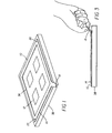
- FIG. 1 is an isometric of a flexible frame on a plate prior to removal
- FIG. 2 is an exploded view of a flexible frame and carrier for pealable deposition mask in accordance with the present invention.
- FIG. 3 depicts a flexible frame during removal of the pealable deposition mask from a plate.
- FIG. 1 is an isometric of a flexible frame 14 having border portions 10 preferably made of aluminum having a central rectangular opening 36 required to permit the deposition of organic materials. Located at one outside corner of the rectangular shaped flexible frame 14 is a grip tab 18 . Depicted in FIG. 1 in two locations at opposing corners of flexible frame 14 there are locator holes 20 . The locator holes 20 serve a duel purpose. As depicted in FIG. 1 the locator holes 20 function as visual alignment holes for the purpose of manually aligning the flexible frame 14 to an alignment target 24 located at opposing corners of the pealable deposition mask 12 .
- the present invention aligns and secures the border portions 10 of the flexible frame 14 to the border portions of pealable deposition mask This facilitates the removal of the flexible frame 14 and secured pealable deposition mask 12 from the plate 38 .
- FIG. 2 corresponding to the locator holes 20 in the flexible frame 14 .
- FIG. 2 depicts an exploded view of a flexible frame 14 having a pealable deposition mask 12 adhesively attached and mounted in a carrier 26 .
- a pealable deposition mask 12 having alignment holes 22 and a target 24 in the form of marks on which a flexible frame 14 is mounted by means of an adhesive layer 16 (see FIG. 3 ).
- the flexible frame 14 having a grip tab 18 to facilitate the removal of the pealable deposition mask 12 to be discussed in detail in FIG. 3 .
- the flexible frame 14 having locator holes 20 are depicted in opposing corners that are used for aligning the pealable deposition mask 12 .
- the pealable deposition mask 12 having an alignment target 24 located in opposing corners of the pealable deposition mask 12 correspond with the alignment holes 22 in the flexible frame 14 .
- the exploded view also depicts a carrier 26 having two pins 28 located in opposing corners of a central pocket 30 that are in alignment with the locator holes 20 in flexible frame 14 .
- the central pocket 30 is configured in a pattern that accepts a flexible frame 14 having a clearance allowance on the perimeter as to not restrict thermal expansion.
- the carrier 26 is depicted having a opening 34 which is in a central location in the carrier 26 bordering pocket 30 .
- This mounting arrangement maintains planarity of the pealable deposition mask 12 during subsequent vacuum deposition of material.
- a keeper 32 which provides a method of sandwiching the flexible frame 14 having the adhesive layer 16 and the pealable deposition mask 12 planar to carrier 26 in manner that does not restrict lateral movement caused by thermal expansion. Thermal expansion occurs during the deposition process. It is understood in the deposition of organic materials through a pealable deposition mask while forming an organic materials through a pealable disposition mask while forming an organic light emitting diodes (OLED) that the temperature differential occurs.
- FIG. 3 depicts the process of removing the pealable deposition mask 12 from the plate 38 using the grip tab 18 located on flexible frame 14 to lift and peel the pealable deposition mask 12 from the plate 38 by manually lifting the grip tab 18 which will flex the flexible frame 14 in a manner that peels the pealable deposition mask 12 from the plate 38 .
- the process of removal is complete and the flexible frame 14 with the pealable deposition mask 12 adhesively attached can now be mounted in carrier 30 .
Abstract
Description
- 10 border portions
- 12 pealable deposition mask
- 14 flexible frame
- 16 adhesive layer
- 18 grip tab
- 20 locator hole
- 22 alignment hole
- 24 alignment target
- 26 carrier
- 28 pin
- 30 central pocket
- 32 keeper
- 34 opening
- 36 central rectangular opening
- 38 plate
Claims (5)
Priority Applications (8)
| Application Number | Priority Date | Filing Date | Title |
|---|---|---|---|
| US10/334,956 US6926840B2 (en) | 2002-12-31 | 2002-12-31 | Flexible frame for mounting a deposition mask |
| TW092131405A TW200415955A (en) | 2002-12-31 | 2003-11-10 | Flexible frame for mounting a deposition mask |
| PCT/US2003/039631 WO2004061149A1 (en) | 2002-12-31 | 2003-12-12 | Flexible frame for mounting a deposition mask |
| CNA2003801080732A CN1732282A (en) | 2002-12-31 | 2003-12-12 | Flexible frame for mounting a deposition mask |
| KR1020057012308A KR20050085929A (en) | 2002-12-31 | 2003-12-12 | Flexible frame for mounting a deposition mask |
| JP2004565424A JP2006512735A (en) | 2002-12-31 | 2003-12-12 | Flexible frame for attaching deposition mask |
| EP03796994A EP1579024B1 (en) | 2002-12-31 | 2003-12-12 | Flexible frame for mounting a deposition mask |
| DE60312385T DE60312385T2 (en) | 2002-12-31 | 2003-12-12 | BENDABLE FRAME FOR MOUNTING AN ARRANGEMENT MASK |
Applications Claiming Priority (1)
| Application Number | Priority Date | Filing Date | Title |
|---|---|---|---|
| US10/334,956 US6926840B2 (en) | 2002-12-31 | 2002-12-31 | Flexible frame for mounting a deposition mask |
Publications (2)
| Publication Number | Publication Date |
|---|---|
| US20040123799A1 US20040123799A1 (en) | 2004-07-01 |
| US6926840B2 true US6926840B2 (en) | 2005-08-09 |
Family
ID=32655212
Family Applications (1)
| Application Number | Title | Priority Date | Filing Date |
|---|---|---|---|
| US10/334,956 Expired - Lifetime US6926840B2 (en) | 2002-12-31 | 2002-12-31 | Flexible frame for mounting a deposition mask |
Country Status (8)
| Country | Link |
|---|---|
| US (1) | US6926840B2 (en) |
| EP (1) | EP1579024B1 (en) |
| JP (1) | JP2006512735A (en) |
| KR (1) | KR20050085929A (en) |
| CN (1) | CN1732282A (en) |
| DE (1) | DE60312385T2 (en) |
| TW (1) | TW200415955A (en) |
| WO (1) | WO2004061149A1 (en) |
Cited By (6)
| Publication number | Priority date | Publication date | Assignee | Title |
|---|---|---|---|---|
| US20060011137A1 (en) * | 2004-07-16 | 2006-01-19 | Applied Materials, Inc. | Shadow frame with mask panels |
| US20070015070A1 (en) * | 2005-07-14 | 2007-01-18 | Seiko Epson Corporation | Manufacturing apparatus for oriented film, liquid crystal device, and electronic device |
| US20100267227A1 (en) * | 2009-04-16 | 2010-10-21 | Jung-Woo Ko | Mask frame assembly for thin film deposition and associated methods |
| US20110139069A1 (en) * | 2009-12-11 | 2011-06-16 | Hong-Kyun Ahn | Mask assembly |
| US20110185965A1 (en) * | 2010-02-03 | 2011-08-04 | Chong-Hyun Park | Mask assembly |
| US20180220684A1 (en) * | 2014-09-19 | 2018-08-09 | Ginny McCormick | Stencil holder apparatus and method |
Families Citing this family (22)
| Publication number | Priority date | Publication date | Assignee | Title |
|---|---|---|---|---|
| CN100464440C (en) * | 2002-06-03 | 2009-02-25 | 三星移动显示器株式会社 | Mask frame assembly of thin layer vacuum evaporation for organic electroluminescent device |
| JP4285456B2 (en) * | 2005-07-20 | 2009-06-24 | セイコーエプソン株式会社 | Mask, mask manufacturing method, film forming method, and electro-optical device manufacturing method |
| KR100662558B1 (en) * | 2005-12-13 | 2006-12-28 | 삼성전자주식회사 | Mask and manufacturing method of display device using the same |
| US20070137568A1 (en) * | 2005-12-16 | 2007-06-21 | Schreiber Brian E | Reciprocating aperture mask system and method |
| US7763114B2 (en) * | 2005-12-28 | 2010-07-27 | 3M Innovative Properties Company | Rotatable aperture mask assembly and deposition system |
| KR101472128B1 (en) * | 2007-12-24 | 2014-12-15 | 엘지디스플레이 주식회사 | Shadow mask frame and apparatus for fabricating organic electro-luminescence display device using the same |
| TWI398533B (en) * | 2009-12-29 | 2013-06-11 | Au Optronics Corp | Shadow mask and method of making the same |
| KR101182440B1 (en) * | 2010-01-11 | 2012-09-12 | 삼성디스플레이 주식회사 | Mask frame assembly for thin film deposition |
| KR101274718B1 (en) | 2010-01-28 | 2013-06-12 | 엘지디스플레이 주식회사 | Deposition Mask Unit and Mask Assembly comprising the same |
| EP2522700A1 (en) | 2011-05-11 | 2012-11-14 | Saint-Gobain Glass France | Water soluble printing paste |
| KR101818647B1 (en) * | 2011-06-14 | 2018-01-16 | 삼성디스플레이 주식회사 | Manufacturing method for organic light emitting display apparatus |
| US9340876B2 (en) * | 2012-12-12 | 2016-05-17 | Applied Materials, Inc. | Mask for deposition process |
| KR102160695B1 (en) * | 2013-05-10 | 2020-09-29 | 삼성디스플레이 주식회사 | Mask |
| CN103882375B (en) * | 2014-03-12 | 2016-03-09 | 京东方科技集团股份有限公司 | A kind of mask plate and preparation method thereof |
| CN106019819A (en) | 2016-07-22 | 2016-10-12 | 京东方科技集团股份有限公司 | Mask plate and making method |
| CN206188877U (en) * | 2016-11-30 | 2017-05-24 | 京东方科技集团股份有限公司 | Mask plate frame and mask plate subassembly |
| KR102217810B1 (en) * | 2017-09-18 | 2021-02-22 | 주식회사 오럼머티리얼 | Producing method of mask integrated frame |
| CN209778978U (en) * | 2017-10-19 | 2019-12-13 | P2I有限公司 | Apparatus or production line for mask substrate |
| KR102371176B1 (en) * | 2018-02-09 | 2022-03-08 | 주식회사 오럼머티리얼 | Method for separating mask adhere to frame |
| CN109023234B (en) * | 2018-08-09 | 2020-08-28 | 深圳市华星光电半导体显示技术有限公司 | Mask plate replacing device and replacing method |
| JP2021175824A (en) * | 2020-03-13 | 2021-11-04 | 大日本印刷株式会社 | Evaluation method of vapor deposition chamber of manufacturing apparatus of organic device, standard mask device and standard substrate used for evaluation method, manufacturing method of standard mask device, manufacturing apparatus of organic device having vapor deposition chamber evaluated by evaluation method, organic device having vapor-deposited layer formed in vapor deposition chamber evaluated by evaluation method, and maintenance method of vapor deposition chamber in manufacturing apparatus of organic device |
| US20220369661A1 (en) * | 2021-05-23 | 2022-11-24 | Ginny McCormick | Silk holder apparatus and method of using silk holder apparatus with stencil holder |
Citations (9)
| Publication number | Priority date | Publication date | Assignee | Title |
|---|---|---|---|---|
| JPS5591972A (en) | 1978-12-28 | 1980-07-11 | Matsushita Electric Ind Co Ltd | Removing method for vacuum deposited metal layer from vacuum deposition mask |
| US5661371A (en) * | 1990-12-31 | 1997-08-26 | Kopin Corporation | Color filter system for light emitting display panels |
| US5945238A (en) * | 1998-02-06 | 1999-08-31 | Clear Logic, Inc. | Method of making a reusable photolithography mask |
| JPH11243274A (en) | 1998-02-25 | 1999-09-07 | Senju Metal Ind Co Ltd | Formation of solder bump and mask for solder bump formation |
| WO1999054786A1 (en) | 1998-04-21 | 1999-10-28 | President And Fellows Of Harvard College | Elastomeric mask and use in fabrication of devices, inlcuding pixelated electroluminescent displays |
| US6146489A (en) * | 1998-11-19 | 2000-11-14 | General Electric Company | Method and apparatus for depositing scintillator material on radiation imager |
| US6475287B1 (en) | 2001-06-27 | 2002-11-05 | Eastman Kodak Company | Alignment device which facilitates deposition of organic material through a deposition mask |
| US6703172B2 (en) * | 2001-10-31 | 2004-03-09 | Mitsui Chemicals, Inc. | Pellicle and producing method of mask with pellicle |
| US6703328B2 (en) * | 2001-01-31 | 2004-03-09 | Renesas Technology Corporation | Semiconductor device manufacturing method |
Family Cites Families (2)
| Publication number | Priority date | Publication date | Assignee | Title |
|---|---|---|---|---|
| DE3115116A1 (en) * | 1980-05-07 | 1982-02-04 | The Perkin-Elmer Corp., 06856 Norwalk, Conn. | Method of producing a mask substrate for use in x-ray lithography |
| KR100382491B1 (en) * | 2000-11-28 | 2003-05-09 | 엘지전자 주식회사 | shadow mask in organic electroluminescence |
-
2002
- 2002-12-31 US US10/334,956 patent/US6926840B2/en not_active Expired - Lifetime
-
2003
- 2003-11-10 TW TW092131405A patent/TW200415955A/en unknown
- 2003-12-12 CN CNA2003801080732A patent/CN1732282A/en active Pending
- 2003-12-12 KR KR1020057012308A patent/KR20050085929A/en not_active Application Discontinuation
- 2003-12-12 EP EP03796994A patent/EP1579024B1/en not_active Expired - Lifetime
- 2003-12-12 WO PCT/US2003/039631 patent/WO2004061149A1/en active IP Right Grant
- 2003-12-12 DE DE60312385T patent/DE60312385T2/en not_active Expired - Lifetime
- 2003-12-12 JP JP2004565424A patent/JP2006512735A/en active Pending
Patent Citations (9)
| Publication number | Priority date | Publication date | Assignee | Title |
|---|---|---|---|---|
| JPS5591972A (en) | 1978-12-28 | 1980-07-11 | Matsushita Electric Ind Co Ltd | Removing method for vacuum deposited metal layer from vacuum deposition mask |
| US5661371A (en) * | 1990-12-31 | 1997-08-26 | Kopin Corporation | Color filter system for light emitting display panels |
| US5945238A (en) * | 1998-02-06 | 1999-08-31 | Clear Logic, Inc. | Method of making a reusable photolithography mask |
| JPH11243274A (en) | 1998-02-25 | 1999-09-07 | Senju Metal Ind Co Ltd | Formation of solder bump and mask for solder bump formation |
| WO1999054786A1 (en) | 1998-04-21 | 1999-10-28 | President And Fellows Of Harvard College | Elastomeric mask and use in fabrication of devices, inlcuding pixelated electroluminescent displays |
| US6146489A (en) * | 1998-11-19 | 2000-11-14 | General Electric Company | Method and apparatus for depositing scintillator material on radiation imager |
| US6703328B2 (en) * | 2001-01-31 | 2004-03-09 | Renesas Technology Corporation | Semiconductor device manufacturing method |
| US6475287B1 (en) | 2001-06-27 | 2002-11-05 | Eastman Kodak Company | Alignment device which facilitates deposition of organic material through a deposition mask |
| US6703172B2 (en) * | 2001-10-31 | 2004-03-09 | Mitsui Chemicals, Inc. | Pellicle and producing method of mask with pellicle |
Cited By (13)
| Publication number | Priority date | Publication date | Assignee | Title |
|---|---|---|---|---|
| US20060011137A1 (en) * | 2004-07-16 | 2006-01-19 | Applied Materials, Inc. | Shadow frame with mask panels |
| US20070015070A1 (en) * | 2005-07-14 | 2007-01-18 | Seiko Epson Corporation | Manufacturing apparatus for oriented film, liquid crystal device, and electronic device |
| US9321074B2 (en) * | 2009-04-16 | 2016-04-26 | Samsung Display Co., Ltd. | Method of manufacturing a mask frame assembly for thin film deposition |
| US8402917B2 (en) * | 2009-04-16 | 2013-03-26 | Samsung Display Co., Ltd. | Mask frame assembly for thin film deposition and associated methods |
| US20130205568A1 (en) * | 2009-04-16 | 2013-08-15 | Jung-Woo Ko | Method of manufacturing a mask frame assembly for thin film deposition |
| US20100267227A1 (en) * | 2009-04-16 | 2010-10-21 | Jung-Woo Ko | Mask frame assembly for thin film deposition and associated methods |
| US20110139069A1 (en) * | 2009-12-11 | 2011-06-16 | Hong-Kyun Ahn | Mask assembly |
| US8646406B2 (en) * | 2009-12-11 | 2014-02-11 | Samsung Display Co., Ltd. | Mask assembly having a frame with support stick |
| US9931666B2 (en) | 2009-12-11 | 2018-04-03 | Samsung Display Co., Ltd. | Mask assembly having frame with support stick |
| US20110185965A1 (en) * | 2010-02-03 | 2011-08-04 | Chong-Hyun Park | Mask assembly |
| US9004002B2 (en) * | 2010-02-03 | 2015-04-14 | Lg Display Co., Ltd. | Mask assembly having a plurality of projections at a boundary of adjacent two deposition masks |
| US20180220684A1 (en) * | 2014-09-19 | 2018-08-09 | Ginny McCormick | Stencil holder apparatus and method |
| US10383350B2 (en) * | 2014-09-19 | 2019-08-20 | Ginny McCormick | Stencil holder apparatus and method |
Also Published As
| Publication number | Publication date |
|---|---|
| US20040123799A1 (en) | 2004-07-01 |
| JP2006512735A (en) | 2006-04-13 |
| TW200415955A (en) | 2004-08-16 |
| EP1579024B1 (en) | 2007-03-07 |
| CN1732282A (en) | 2006-02-08 |
| WO2004061149A1 (en) | 2004-07-22 |
| DE60312385D1 (en) | 2007-04-19 |
| KR20050085929A (en) | 2005-08-29 |
| DE60312385T2 (en) | 2007-11-29 |
| EP1579024A1 (en) | 2005-09-28 |
Similar Documents
| Publication | Publication Date | Title |
|---|---|---|
| US6926840B2 (en) | Flexible frame for mounting a deposition mask | |
| US6475287B1 (en) | Alignment device which facilitates deposition of organic material through a deposition mask | |
| US6589382B2 (en) | Aligning mask segments to provide a stitched mask for producing OLED devices | |
| JP3651432B2 (en) | Mask, manufacturing method thereof, and manufacturing method of electroluminescence device | |
| US20030108805A1 (en) | Aligning mask segments to provide an assembled mask for producing oled devices | |
| US4915057A (en) | Apparatus and method for registration of shadow masked thin-film patterns | |
| US4615781A (en) | Mask assembly having mask stress relieving feature | |
| US20050118788A1 (en) | Mask, method for manufacturing thereof, method for manufacturing organic electroluminescent device, and organic electroluminescent device | |
| WO2019202902A1 (en) | Vapor deposition mask, vapor deposition mask with frame, vapor deposition mask preparatory body, manufacturing method for vapor deposition mask, manufacturing method for organic semiconductor element, manufacturing method for organic el display, and pattern formation method | |
| TW585011B (en) | Mask and method of manufacturing the same, and method of manufacturing electro-luminescence (EL) device | |
| CN109097730B (en) | Mask plate and manufacturing method thereof | |
| JP2003272839A (en) | Manufacturing method of masking member for evaporation treatment | |
| JP2006152339A (en) | Vapor deposition mask structural body manufacturing method | |
| US10985341B2 (en) | Encapsulating thin film, production method thereof, and method for encapsulating display panel | |
| WO2005093814A1 (en) | Oled donor sheet having rigid edge frame | |
| EP0780225B1 (en) | Plastic mask unit for paste printing and method of fabricating such plastic mask unit | |
| JP4235823B2 (en) | Mask manufacturing method | |
| JP4380326B2 (en) | Deposition mask for organic EL | |
| US10930546B2 (en) | TFT substrate and method for manufacturing the same | |
| CN115627444A (en) | Mask assembly and mask assembly carrying method | |
| KR20030044664A (en) | A shadow mask for a large size OELD and forming method of thereof | |
| JPS6358348A (en) | Surface protector for reticle |
Legal Events
| Date | Code | Title | Description |
|---|---|---|---|
| AS | Assignment |
Owner name: EASTMAN KODAK COMPANY, NEW YORK Free format text: ASSIGNMENT OF ASSIGNORS INTEREST;ASSIGNOR:CLARK, THOMAS K.;REEL/FRAME:013646/0395 Effective date: 20021220 |
|
| FEPP | Fee payment procedure |
Free format text: PAYOR NUMBER ASSIGNED (ORIGINAL EVENT CODE: ASPN); ENTITY STATUS OF PATENT OWNER: LARGE ENTITY |
|
| STCF | Information on status: patent grant |
Free format text: PATENTED CASE |
|
| FEPP | Fee payment procedure |
Free format text: PAYOR NUMBER ASSIGNED (ORIGINAL EVENT CODE: ASPN); ENTITY STATUS OF PATENT OWNER: LARGE ENTITY Free format text: PAYER NUMBER DE-ASSIGNED (ORIGINAL EVENT CODE: RMPN); ENTITY STATUS OF PATENT OWNER: LARGE ENTITY |
|
| FPAY | Fee payment |
Year of fee payment: 4 |
|
| FEPP | Fee payment procedure |
Free format text: PAYOR NUMBER ASSIGNED (ORIGINAL EVENT CODE: ASPN); ENTITY STATUS OF PATENT OWNER: LARGE ENTITY Free format text: PAYER NUMBER DE-ASSIGNED (ORIGINAL EVENT CODE: RMPN); ENTITY STATUS OF PATENT OWNER: LARGE ENTITY |
|
| AS | Assignment |
Owner name: GLOBAL OLED TECHNOLOGY LLC,DELAWARE Free format text: ASSIGNMENT OF ASSIGNORS INTEREST;ASSIGNOR:EASTMAN KODAK COMPANY;REEL/FRAME:023998/0368 Effective date: 20100122 Owner name: GLOBAL OLED TECHNOLOGY LLC, DELAWARE Free format text: ASSIGNMENT OF ASSIGNORS INTEREST;ASSIGNOR:EASTMAN KODAK COMPANY;REEL/FRAME:023998/0368 Effective date: 20100122 |
|
| FPAY | Fee payment |
Year of fee payment: 8 |
|
| FPAY | Fee payment |
Year of fee payment: 12 |