US6922231B1 - Receiver optical sub-assembly with diagnostic signal - Google Patents
Receiver optical sub-assembly with diagnostic signal Download PDFInfo
- Publication number
- US6922231B1 US6922231B1 US10/350,494 US35049403A US6922231B1 US 6922231 B1 US6922231 B1 US 6922231B1 US 35049403 A US35049403 A US 35049403A US 6922231 B1 US6922231 B1 US 6922231B1
- Authority
- US
- United States
- Prior art keywords
- signal
- pin
- amplifier
- electro
- assembly
- Prior art date
- Legal status (The legal status is an assumption and is not a legal conclusion. Google has not performed a legal analysis and makes no representation as to the accuracy of the status listed.)
- Expired - Lifetime, expires
Links
- 230000003287 optical effect Effects 0.000 title claims abstract description 47
- 239000003990 capacitor Substances 0.000 claims description 17
- 238000000034 method Methods 0.000 claims description 15
- 230000005540 biological transmission Effects 0.000 claims description 13
- 238000012544 monitoring process Methods 0.000 claims description 8
- 230000008878 coupling Effects 0.000 claims description 7
- 238000010168 coupling process Methods 0.000 claims description 7
- 238000005859 coupling reaction Methods 0.000 claims description 7
- 230000004044 response Effects 0.000 claims description 5
- 239000000835 fiber Substances 0.000 description 8
- 238000010586 diagram Methods 0.000 description 7
- 230000002547 anomalous effect Effects 0.000 description 5
- 239000004593 Epoxy Substances 0.000 description 3
- 230000000875 corresponding effect Effects 0.000 description 3
- PCHJSUWPFVWCPO-UHFFFAOYSA-N gold Chemical compound [Au] PCHJSUWPFVWCPO-UHFFFAOYSA-N 0.000 description 3
- 239000010931 gold Substances 0.000 description 3
- 229910052737 gold Inorganic materials 0.000 description 3
- 239000010410 layer Substances 0.000 description 3
- 238000005259 measurement Methods 0.000 description 3
- 238000001514 detection method Methods 0.000 description 2
- 239000011521 glass Substances 0.000 description 2
- 238000009413 insulation Methods 0.000 description 2
- 229910000679 solder Inorganic materials 0.000 description 2
- 238000012935 Averaging Methods 0.000 description 1
- 229910000530 Gallium indium arsenide Inorganic materials 0.000 description 1
- 230000008033 biological extinction Effects 0.000 description 1
- 238000005219 brazing Methods 0.000 description 1
- 230000015556 catabolic process Effects 0.000 description 1
- 239000000919 ceramic Substances 0.000 description 1
- 230000008859 change Effects 0.000 description 1
- 238000004891 communication Methods 0.000 description 1
- 230000002596 correlated effect Effects 0.000 description 1
- 238000006731 degradation reaction Methods 0.000 description 1
- 238000005286 illumination Methods 0.000 description 1
- 229910001092 metal group alloy Inorganic materials 0.000 description 1
- 239000013307 optical fiber Substances 0.000 description 1
- 230000037361 pathway Effects 0.000 description 1
- 238000012545 processing Methods 0.000 description 1
- 230000009467 reduction Effects 0.000 description 1
- 239000002356 single layer Substances 0.000 description 1
Images


Classifications
-
- H—ELECTRICITY
- H01—ELECTRIC ELEMENTS
- H01L—SEMICONDUCTOR DEVICES NOT COVERED BY CLASS H10
- H01L31/00—Semiconductor devices sensitive to infrared radiation, light, electromagnetic radiation of shorter wavelength or corpuscular radiation and specially adapted either for the conversion of the energy of such radiation into electrical energy or for the control of electrical energy by such radiation; Processes or apparatus specially adapted for the manufacture or treatment thereof or of parts thereof; Details thereof
- H01L31/02—Details
- H01L31/02016—Circuit arrangements of general character for the devices
Definitions
- the present invention relates to fiber optic receivers and, in particular, a fiber optic receiver with a diagnostic signal.
- optical transmission pathways have been designed and built that encode data in a modulated light signal and transmit the light signal with an optical waveguide, such as a glass or plastic fiber.
- the data is encoded and transmitted by a transceiver optical sub-assembly (TOSA) operating with an encoder, and received and decoded by a receiver optical sub-assembly (ROSA) operating with a decoder.
- TOSA transceiver optical sub-assembly
- ROSA receiver optical sub-assembly
- a decoder typically included in the TOSA is a diode laser, lens, and a circuit for driving the laser.
- Typically included in the ROSA is a lens, photodetector and amplifier for amplifying the photocurrent signal produced by the photodetector.
- the form factor for a ROSA is generally a TO-46 can package, which is a 4-pin output package designed to mate with a fiber optic cable and corresponding LC connector.
- the four pins are usually dedicated to the positive polarity data, the inverse polarity data, the supply voltage, and ground.
- the positive polarity data and inverse polarity data pins can be AC coupled to a data detector, which measures the optical modulated amplitude (OMA).
- OMA optical modulated amplitude
- the amplitude of the signal modulation may be measured by a radio frequency (rf) amplifier, and correlated to a root-mean-square (rms) value for the amplitude of the optical (AC) modulation.
- rf radio frequency
- rms root-mean-square
- Such rf measurements can be sufficiently accurate indicators of the average detected optical power for relatively high power signals, however their accuracy is poor for lower input power levels.
- the OMA measurement is a non-linear method, using an rf power amplifier which amplifies the noise power as well as the signal power.
- the power level is low, it is difficult to separate the noise power from the signal power. Therefore it is difficult to detect a fault situation, such as a broken or intermittent link occurring on an optical transmission line, using optical modulation amplitude alone, because the noise contributes substantially to the overall signal level. Therefore techniques which measure the (AC) modulation amplitude are relatively poor indicators of changes in the attenuation of the data transmission channel.
- a receiver optical sub-assembly for receiving an optical data signal from a fiber optic input line.
- the sub-assembly includes an electro-optic transducer, configured to produce an electrical data signal in response to a received optical data signal.
- the transducer includes a cathode and anode. The cathode of the transducer can be coupled to a diagnostic signal pin, for outputting a diagnostic signal indicative of the average received optical power in the optical data signal.
- the receiver optical sub-assembly further includes an amplifier with an input coupled to the anode of the electro-optic transducer, and operable to amplify electrical data signals produced by the electro-optic transducer, the amplifier having an inverted polarity data output pad coupled to an inverted polarity data output pin, and a non-inverted polarity data output pad coupled to a non-inverted polarity data output pin.
- the ROSA according to the present invention therefore has an additional diagnostic pin added to the conventional four-pin connector, in which the four usual pins carry supply voltage, ground, inverted polarity output data, and non-inverted polarity output data.
- the fifth pin carries the diagnostic signal, which is related to the average received power, and therefore has a DC signal level in addition to the usual optical modulation amplitude.
- the modulation amplitude corresponds to the data pattern
- the average received power corresponds to the input power and attenuation from the data channel. Monitoring the average received power allows the user to monitor the condition of the data channel, and to detect anomalous increases in the attenuation, as would result, for example, from damaged or faulty links in the data channel.
- the average power measurement is a linear method, very good accuracy can be obtained, and calibration of the signal is straightforward. Even at low signal levels, the signal may be separated from the noise using simple signal processing algorithms, such as averaging.
- the average power is a direct indication of signal strength or link attenuation.
- the receiver optical sub-assembly with diagnostic signal may be included in a larger system for monitoring the performance of a data channel in terms of its attenuation.
- the diagnostic signal indicative of the average optical power of the incoming transmitted data signal is a current generated by the electro-optic transducer. This current is applied to an external resistor, and the voltage drop across the resistor is amplified by an amplifier. The amplified value may then be digitized by an analog-to-digital converter, and output to a monitoring computer. The value detected by the computer may then be compared to a reference value, and a warning flag asserted if the level drops below the reference value.
- the receiver optical sub-assembly with diagnostic signal can be used to provide early warning of faults occurring in the data transmission channel, as anomalous changes in the attenuation of the channel.
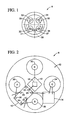
- FIG. 1 is a mechanical drawing of the header of the 5-pin ROSA, according to an embodiment of the present invention.
- FIG. 2 is a wirebond diagram of the circuit connections of the 5-pin ROSA according to an embodiment of the present invention.
- FIG. 3 is a simplified schematic diagram of the 5-pin ROSA embodiment of FIG. 2 .
- FIG. 4 is a schematic of a typical application of the present invention.
- a fiber optic receiver apparatus in which an additional pin is provided to output the average detected power level of the input power of the optical data signal is presented.
- the additional pin is connected to an electrode of the electro-optical transducer, which is the photodetector used to measure the incoming light levels.
- This additional pin will provide the diagnostic signal to external detection circuitry, indicative of the average optical power received by the photodetector. Therefore, while the anode of the photodetector is conventionally coupled to a trans-impedance amplifier (TIA) input pad, the cathode of the detector is coupled to the additional pin provided for its output. This pin output may then be digitized and monitored by an external computer to detect faults occurring in the transmission path, which results in an anomalous reduction of the average transmitted optical power.
- TIA trans-impedance amplifier
- FIG. 1 is a mechanical drawing of a TO-46 connector 8 with 5 pins, according to an embodiment of this invention.
- the TO-46 style connector is only an example, and that other form factor connectors may be used to house a receiving apparatus according to the present invention.
- the 5-pin ROSA 8 has 4 insulated pins 30 , 32 , 34 , and 36 which protrude through a metallic header 42 , and a ground pin 38 which is in electrical contact with the header.
- the insulation may be a layer of glass, which isolates the metallic pins from the metallic header.
- the header 42 is the surface which supports other components of the receiving apparatus, including an amplifier 10 , two single layer ceramic (SLC) capacitors 12 and 14 , and a photodetector 16 (see FIG. 2 ).
- the SLC capacitors are metallized on the two opposing surfaces, for connection with the other components of the circuit.
- FIG. 1 shows that whereas the other four pins 30 , 32 , 34 , and 36 are insulated from the metallic header by insulation layers 31 , 33 , 35 and 37 , pin 38 is in direct electrical contact with the metal alloy of header 42 .
- the electrical connection may be made by brazing the metallic surface of pin 38 to the metallic surface of header 42 .
- the diameter of the insulating layers 31 , 33 , 35 , and 37 may be, for example, 1.2 mm, around a central pin bore 30 , 32 , 34 , and 36 of 0.4 mm, as indicated in FIG. 1 .
- the pins 30 , 32 , 34 , and 36 extend through header 42 and to an elevation of 0.3 mm above header 42 to provide an area for wire bonding to the pins.
- FIG. 2 is a wirebond diagram showing the wirebond connections for a circuit embodiment of the present invention.
- the ROSA 8 includes an electro-optic transducer, or photodetector 16 , and an amplifier 10 which amplifies the signal produced by the photodetector 16 in response to illumination by the incoming laser light. Only the four insulated pins 30 , 32 , 34 , and 36 are shown in FIG. 2 , because the ground pin 38 is obscured by the body of the amplifier 10 , which lies directly overtop of pin 38 in this embodiment.
- the photodetector 16 may be a P-type, Intrinsic, N-type (P-I-N) photodetector, for example an InGaAs PIN detector.
- the detector 16 is mounted electrically, by solder or conductive epoxy, to the top electrode of one of the SLC capacitors 12 .
- the other electrode of the SLC capacitor is connected electrically to the metallic header 42 lying beneath it.
- the center of the photodetector is located in the approximate center of the header, to intercept the focused rays coming from the input fiber line (not shown), through a lens mounted in the ferrule of the input LC connector (not shown), or in the ROSA 8.
- the amplifier 10 in this embodiment is a trans-impedance amplifier (TIA), for example the MAX3864 available from Maxim Integrated Products of Sunnyvale, Calif.
- the trans-impedance amplifier converts current signals input from the light receiving photodetector 16 to voltage signals.
- the TIA may be a bare die, with contact pads 18 , 20 , 22 , 24 , 26 , and 28 .
- the contact pads are metallized areas on the chip to which a gold ball bond may be made.
- Pad 18 is the input pad, and is coupled to the anode of the photodetector 16 by a gold ball bonded wire.
- the cathode of the photodetector is soldered or bonded with conductive epoxy to one electrode of SLC capacitor 12 .
- the other electrode of the SLC capacitor 12 is bonded to the header 42 , and thereby to the case ground.
- Power is provided to the amplifier 10 by the power supply pin 34 , which is one of the four insulated pins in the 5-pin ROSA 8.
- the supply voltage is delivered by post 34 of the ROSA 8, to the TIA via contact pad 20 , across the electrode of the second SLC capacitor 14 .
- the other electrode of capacitor 14 is solder bonded or attached with conductive epoxy to the case ground and header surface 42 .
- Bias voltage is supplied to the photodetector by pin 32 , which will also carry the average photocurrent signal to circuitry external to the ROSA.
- the bias voltage is delivered by coupling pin 32 across the electrode of SLC capacitor 12 , which is then coupled to the cathode of the photodetector 16 .
- Each of these connections may be made, for example, by gold ball bonding of a wire between the pad and pin.
- the other wirebonds are as shown in FIG. 2 .
- the TIA outputs a differential signal corresponding to the optical modulation amplitude of the signal generated by the photodetector.
- Post 30 is coupled to the inverse polarity data output line 26 of the TIA, and post 36 is coupled to the non-inverted polarity of the data output line 24 of the TIA.
- Ground pads 22 and 28 of the TIA are coupled to the header surface 42 , and thereby to the case ground.
- FIG. 3 is a simplified schematic diagram corresponding to the wirebond diagram of FIG. 2 .
- the schematic shows the anode of photodetector 16 , coupled to the input pad 18 of the TIA amplifier 10 .
- the cathode of the photodetector 16 is coupled to SLC capacitor 12 and to pin 32 of the ROSA, to provide the average power signal for external diagnostic circuitry.
- the other electrode of SLC capacitor 12 is connected to ground via the header surface 42 .
- the TIA converts the electrical signals generated by the photodetector 16 in response to the modulated intensity waveform of the incident light beam, into an amplified voltage signal which is differentially output on pins 30 and 36 of the ROSA.
- the ground pins 22 and 28 of the TIA are coupled to the case ground, which is further coupled to the ground pin 38 of the 5-pin ROSA 8.
- capacitors 12 and 14 are coupled to the case ground by direct connection to the header surface 42 .
- the values of the capacitors may be for example 1000 pf. It is clear from the schematic circuit diagram of FIG. 3 , that the pin 32 of the ROSA serves two purposes: to deliver the DC bias voltage to the photodetector 16 , and to carry the average photocurrent signal produced by the laser light impinging on photodetector 16 .
- FIG. 4 shows an exemplary application using the present invention.
- data outputs from the TIA 10 are routed to a data detector 50 as Rd+ (non-inverted data output) on pin 36 and Rd ⁇ (inverted data output) on pin 30 of ROSA 8.
- the signal output on pin 32 corresponds to the average detected power of the incoming data signal, as measured by the PIN photodetector 16 .
- Pin 32 also carries the bias voltage from voltage supply source 42 .
- the current generated on pin 32 in connection with the cathode of the photodetector 16 is applied to an external sense resistor 44 and the voltage difference is measured across the resistor 44 .
- the resistance value of the external sense resistor may be, for example, 200 ⁇ .
- the signal measured across resistor 44 is amplified by a current-sensing amplifier 46 , for example the MAX4372TEUK, also available from Maxim Integrated Products of Sunnyvale, Calif.
- the current-sensing amplifier 46 amplifies the signal to generate R in , which may then be digitized by an analog-to-digital converter (ADC, not shown), and the value is input to a computer (not shown).
- ADC analog-to-digital converter
- the computer can then compare the measured value to a reference value, and assert a warning flag if the measured level drops below the reference level.
- the signal on pin 32 of the ROSA corresponds to the average detected photocurrent, it can provide diagnostic information to the computer as to the status of the transmission line delivering the optical data signal. For example if an optical link is damaged or intermittent, this condition is readily detected by an anomalous drop in the average power detected in the optical signal.
- Other detection means which measure only AC coupled signals, cannot detect a change in the average signal level, and are therefore relatively insensitive to changes in the condition of the transmission channel, such as degraded links. In this situation, no warning of imminent failure may be available, until the data channel fails.
- Using the average transmitted intensity early warning of transmission channel degradation is possible, by detecting anomalous changes in the average transmitted intensity of the input light beam.
- the 5-pin ROSA described herein is designed, for example, to mate with a conventional optical fiber delivered by, e.g., an LC connector.
- the LC connector may mate to the outer surface of the TO-46 package, and center the input fiber on the aperture of the photodetector.
- the ROSA may also include a lens for focusing the light rays onto the photodetector.
- this invention is not limited to the embodiments described above.
- the invention is not limited to the particular style of connector, such as the TO-46, or the particular components included in the receiver optical sub-assembly, such as the MAX3864.
- the invention is not limited to a particular transmission wavelength or other optical standards.
- Other embodiments and variations within the scope of the invention, as defined by the appended claims, will occur to practitioners in view of the disclosure herein.
Abstract
Description
Claims (26)
Priority Applications (1)
| Application Number | Priority Date | Filing Date | Title |
|---|---|---|---|
| US10/350,494 US6922231B1 (en) | 2003-01-23 | 2003-01-23 | Receiver optical sub-assembly with diagnostic signal |
Applications Claiming Priority (1)
| Application Number | Priority Date | Filing Date | Title |
|---|---|---|---|
| US10/350,494 US6922231B1 (en) | 2003-01-23 | 2003-01-23 | Receiver optical sub-assembly with diagnostic signal |
Publications (1)
| Publication Number | Publication Date |
|---|---|
| US6922231B1 true US6922231B1 (en) | 2005-07-26 |
Family
ID=34748681
Family Applications (1)
| Application Number | Title | Priority Date | Filing Date |
|---|---|---|---|
| US10/350,494 Expired - Lifetime US6922231B1 (en) | 2003-01-23 | 2003-01-23 | Receiver optical sub-assembly with diagnostic signal |
Country Status (1)
| Country | Link |
|---|---|
| US (1) | US6922231B1 (en) |
Cited By (13)
| Publication number | Priority date | Publication date | Assignee | Title |
|---|---|---|---|---|
| US20050191879A1 (en) * | 2004-02-27 | 2005-09-01 | Ice Donald A. | Lead frame for connecting optical sub-assembly to printed circuit board |
| US20050189400A1 (en) * | 2004-02-27 | 2005-09-01 | Ice Donald A. | Methods for manufacturing optical modules using lead frame connectors |
| US20050188535A1 (en) * | 2004-02-27 | 2005-09-01 | Ice Donald A. | Methods for manufacturing lead frame connectors for optical transceiver modules |
| US20050221637A1 (en) * | 2004-02-27 | 2005-10-06 | Ice Donald A | Dual segment molded lead frame connector for optical transceiver modules |
| US20050232641A1 (en) * | 2004-02-27 | 2005-10-20 | Ice Donald A | Methods for manufacturing lead frame connectors for optical transceiver modules |
| US20060024005A1 (en) * | 2004-02-27 | 2006-02-02 | Ice Donald A | Optical transceiver module having a dual segment molded lead frame connector |
| US20060249820A1 (en) * | 2005-04-29 | 2006-11-09 | Finisar Corporation | Molded lead frame connector with one or more passive components |
| US20060252313A1 (en) * | 2005-04-29 | 2006-11-09 | Finisar Corporation | Molded lead frame connector with mechanical attachment members |
| US20090245789A1 (en) * | 2005-02-28 | 2009-10-01 | International Business Machines Corporation | Methods and Apparatus for Optical Modulation Amplitude Measurement |
| US20090247010A1 (en) * | 2008-03-27 | 2009-10-01 | Robert Hartzell | Method and Apparatus to Provide Electromagnetic Interference Shielding of Optical-Electrical Module |
| US7757929B2 (en) | 2004-02-27 | 2010-07-20 | Finisar Corporation | Methods for manufacturing optical modules having an optical sub-assembly |
| US8200100B2 (en) | 2009-01-19 | 2012-06-12 | Avago Technologies Fiber Ip (Singapore) Pte. Ltd | Systems and methods for diagnostic monitoring of optical modulation amplitude at an optical receiver using automatic gain control |
| US20180172933A1 (en) * | 2016-12-20 | 2018-06-21 | Oclaro Japan, Inc. | Optical module and optical transmission equipment |
Citations (3)
| Publication number | Priority date | Publication date | Assignee | Title |
|---|---|---|---|---|
| US5023947A (en) * | 1989-11-01 | 1991-06-11 | At&T Bell Laboratories | Optical equalization receiver for lightwave communication systems |
| US6069686A (en) * | 1997-07-31 | 2000-05-30 | Virginia Tech Intellectual Properties, Inc. | Self-calibrating optical fiber pressure, strain and temperature sensors |
| US6639482B2 (en) * | 2000-09-21 | 2003-10-28 | Siemens Aktiengesellschaft | Method for regulating the working point of a modulator and associated drive unit |
-
2003
- 2003-01-23 US US10/350,494 patent/US6922231B1/en not_active Expired - Lifetime
Patent Citations (3)
| Publication number | Priority date | Publication date | Assignee | Title |
|---|---|---|---|---|
| US5023947A (en) * | 1989-11-01 | 1991-06-11 | At&T Bell Laboratories | Optical equalization receiver for lightwave communication systems |
| US6069686A (en) * | 1997-07-31 | 2000-05-30 | Virginia Tech Intellectual Properties, Inc. | Self-calibrating optical fiber pressure, strain and temperature sensors |
| US6639482B2 (en) * | 2000-09-21 | 2003-10-28 | Siemens Aktiengesellschaft | Method for regulating the working point of a modulator and associated drive unit |
Cited By (28)
| Publication number | Priority date | Publication date | Assignee | Title |
|---|---|---|---|---|
| US7311530B2 (en) | 2004-02-27 | 2007-12-25 | Finisar Corporation | Dual segment molded lead frame connector for optical transceiver modules |
| US20050188535A1 (en) * | 2004-02-27 | 2005-09-01 | Ice Donald A. | Methods for manufacturing lead frame connectors for optical transceiver modules |
| US7144259B2 (en) * | 2004-02-27 | 2006-12-05 | Finisar Corporation | Optical transceiver module having a dual segment molded lead frame connector |
| US20070003195A1 (en) * | 2004-02-27 | 2007-01-04 | Finisar Corporation | Transceiver module having a dual segment lead frame connector |
| US20050232641A1 (en) * | 2004-02-27 | 2005-10-20 | Ice Donald A | Methods for manufacturing lead frame connectors for optical transceiver modules |
| US20060024005A1 (en) * | 2004-02-27 | 2006-02-02 | Ice Donald A | Optical transceiver module having a dual segment molded lead frame connector |
| US7097468B2 (en) | 2004-02-27 | 2006-08-29 | Finisar Corporation | Lead frame for connecting optical sub-assembly to printed circuit board |
| US7757929B2 (en) | 2004-02-27 | 2010-07-20 | Finisar Corporation | Methods for manufacturing optical modules having an optical sub-assembly |
| US7562804B2 (en) * | 2004-02-27 | 2009-07-21 | Finisar Corporation | Methods for manufacturing optical modules using lead frame connectors |
| US20050189400A1 (en) * | 2004-02-27 | 2005-09-01 | Ice Donald A. | Methods for manufacturing optical modules using lead frame connectors |
| US20050221637A1 (en) * | 2004-02-27 | 2005-10-06 | Ice Donald A | Dual segment molded lead frame connector for optical transceiver modules |
| US7229295B2 (en) | 2004-02-27 | 2007-06-12 | Finisar Corporation | Transceiver module having a dual segment lead frame connector |
| US7503112B2 (en) | 2004-02-27 | 2009-03-17 | Finisar Corporation | Methods for manufacturing lead frame connectors for optical transceiver modules |
| US7370414B2 (en) | 2004-02-27 | 2008-05-13 | Finisar Corporation | Methods for manufacturing lead frame connectors for optical transceiver modules |
| US20050191879A1 (en) * | 2004-02-27 | 2005-09-01 | Ice Donald A. | Lead frame for connecting optical sub-assembly to printed circuit board |
| US20090245789A1 (en) * | 2005-02-28 | 2009-10-01 | International Business Machines Corporation | Methods and Apparatus for Optical Modulation Amplitude Measurement |
| JP4755656B2 (en) * | 2005-02-28 | 2011-08-24 | インターナショナル・ビジネス・マシーンズ・コーポレーション | Method and apparatus for light modulation amplitude measurement |
| US7885540B2 (en) * | 2005-02-28 | 2011-02-08 | International Business Machines Corporation | Methods and apparatus for optical modulation amplitude measurement |
| US7473107B2 (en) | 2005-04-29 | 2009-01-06 | Finisar Corporation | Molded lead frame connector with mechanical attachment members |
| US7540747B2 (en) | 2005-04-29 | 2009-06-02 | Finisar Corporation | Molded lead frame connector with one or more passive components |
| US20060252313A1 (en) * | 2005-04-29 | 2006-11-09 | Finisar Corporation | Molded lead frame connector with mechanical attachment members |
| US20060249820A1 (en) * | 2005-04-29 | 2006-11-09 | Finisar Corporation | Molded lead frame connector with one or more passive components |
| US20090247010A1 (en) * | 2008-03-27 | 2009-10-01 | Robert Hartzell | Method and Apparatus to Provide Electromagnetic Interference Shielding of Optical-Electrical Module |
| US7837503B2 (en) | 2008-03-27 | 2010-11-23 | Opnext, Inc. | Method and apparatus to provide electromagnetic interference shielding of optical-electrical module |
| US8200100B2 (en) | 2009-01-19 | 2012-06-12 | Avago Technologies Fiber Ip (Singapore) Pte. Ltd | Systems and methods for diagnostic monitoring of optical modulation amplitude at an optical receiver using automatic gain control |
| US8346101B2 (en) | 2009-01-19 | 2013-01-01 | Avago Technologies Fiber Ip (Singapore) Pte. Ltd | Systems and methods for diagnostic monitoring of optical modulation amplitude at an optical receiver using automatic gain control |
| US20180172933A1 (en) * | 2016-12-20 | 2018-06-21 | Oclaro Japan, Inc. | Optical module and optical transmission equipment |
| US10444452B2 (en) * | 2016-12-20 | 2019-10-15 | Lumentum Japan, Inc. | Optical module and optical transmission equipment |
Similar Documents
| Publication | Publication Date | Title |
|---|---|---|
| US6922231B1 (en) | Receiver optical sub-assembly with diagnostic signal | |
| US7002131B1 (en) | Methods, systems and apparatus for measuring average received optical power | |
| EP0940655B1 (en) | Measuring sensor with at least one optical fiber, measuring device and installation using at least same | |
| WO2010061906A1 (en) | Electric field measuring device | |
| US6384590B1 (en) | Light receiving circuit for use in electro-optic sampling oscilloscope | |
| US6487327B1 (en) | Optical fiber connector monitor apparatus | |
| US6948865B2 (en) | Optical module and method of manufacturing the same | |
| CN103529524A (en) | Optical signal receiving detector and manufacturing method thereof | |
| US5142401A (en) | Apparatus and method for a linear, wideband sensitive optical receiver | |
| US6954569B2 (en) | Butt joined electronic assembly and module | |
| JP3688544B2 (en) | Measurement signal output device | |
| CN113447052A (en) | Light receiving assembly and light sensing equipment | |
| US6342783B1 (en) | Electrooptic probe | |
| US7140784B2 (en) | Rosa alignment using DC or low frequency optical source | |
| CN114383641B (en) | Optical sensing demodulation module and optical sensing system | |
| Vasey et al. | A 12-channel analog optical-receiver module | |
| JP6268865B2 (en) | Inspection method, inspection system, and inspection substrate | |
| JP2000082828A (en) | Optical receiver and optical transmission module | |
| US20220221664A1 (en) | Method of manufacturing light receiving module | |
| US20010022339A1 (en) | Probe signal outputting apparatus | |
| RU195171U1 (en) | Optoelectronic module | |
| KR100479851B1 (en) | Method Of Active Alignment For An Optical Module And Apparatus Thereof | |
| JPH065888A (en) | Photodetector and failure monitoring system for electric equipment using the photodetector | |
| JPH0980083A (en) | Signal waveform measuring equipment for printed board | |
| KR100694294B1 (en) | Opticap sub assembly based on silicon optical benches and optical transceiver using the same |
Legal Events
| Date | Code | Title | Description |
|---|---|---|---|
| AS | Assignment |
Owner name: PINE PHOTONICS COMMUNICATIONS, INC., CALIFORNIA Free format text: ASSIGNMENT OF ASSIGNORS INTEREST;ASSIGNORS:WANG, XIANGZHONG;HARTZELL, ROBERT P.;REEL/FRAME:013710/0127 Effective date: 20030121 |
|
| AS | Assignment |
Owner name: OPNEXT, INC., CALIFORNIA Free format text: ASSIGNMENT OF ASSIGNORS INTEREST;ASSIGNOR:PINE PHOTONICS COMMUNICATIONS, INC.;REEL/FRAME:014950/0691 Effective date: 20040128 |
|
| STCF | Information on status: patent grant |
Free format text: PATENTED CASE |
|
| FPAY | Fee payment |
Year of fee payment: 4 |
|
| FPAY | Fee payment |
Year of fee payment: 8 |
|
| FPAY | Fee payment |
Year of fee payment: 12 |
|
| AS | Assignment |
Owner name: OCLARO FIBER OPTICS, INC., CALIFORNIA Free format text: CHANGE OF NAME;ASSIGNOR:OPNEXT, INC.;REEL/FRAME:046416/0022 Effective date: 20151216 |
|
| AS | Assignment |
Owner name: DEUTSCHE BANK AG NEW YORK BRANCH, AS COLLATERAL AGENT, NEW YORK Free format text: PATENT SECURITY AGREEMENT;ASSIGNORS:LUMENTUM OPERATIONS LLC;OCLARO FIBER OPTICS, INC.;OCLARO, INC.;REEL/FRAME:047788/0511 Effective date: 20181210 Owner name: DEUTSCHE BANK AG NEW YORK BRANCH, AS COLLATERAL AG Free format text: PATENT SECURITY AGREEMENT;ASSIGNORS:LUMENTUM OPERATIONS LLC;OCLARO FIBER OPTICS, INC.;OCLARO, INC.;REEL/FRAME:047788/0511 Effective date: 20181210 |
|
| AS | Assignment |
Owner name: LUMENTUM FIBER OPTICS INC., CALIFORNIA Free format text: CHANGE OF NAME;ASSIGNOR:OCLARO FIBER OPTICS, INC.;REEL/FRAME:049843/0453 Effective date: 20190603 |
|
| AS | Assignment |
Owner name: OCLARO FIBER OPTICS, INC., CALIFORNIA Free format text: RELEASE BY SECURED PARTY;ASSIGNOR:DEUTSCHE AG NEW YORK BRANCH;REEL/FRAME:051287/0556 Effective date: 20191212 Owner name: LUMENTUM OPERATIONS LLC, CALIFORNIA Free format text: RELEASE BY SECURED PARTY;ASSIGNOR:DEUTSCHE AG NEW YORK BRANCH;REEL/FRAME:051287/0556 Effective date: 20191212 Owner name: OCLARO, INC., CALIFORNIA Free format text: RELEASE BY SECURED PARTY;ASSIGNOR:DEUTSCHE AG NEW YORK BRANCH;REEL/FRAME:051287/0556 Effective date: 20191212 |