US6917533B2 - Radiation-hardened programmable device - Google Patents
Radiation-hardened programmable device Download PDFInfo
- Publication number
- US6917533B2 US6917533B2 US10/045,571 US4557101A US6917533B2 US 6917533 B2 US6917533 B2 US 6917533B2 US 4557101 A US4557101 A US 4557101A US 6917533 B2 US6917533 B2 US 6917533B2
- Authority
- US
- United States
- Prior art keywords
- customer
- memory
- data pattern
- radiation
- transistor
- Prior art date
- Legal status (The legal status is an assumption and is not a legal conclusion. Google has not performed a legal analysis and makes no representation as to the accuracy of the status listed.)
- Expired - Lifetime, expires
Links
- 238000000034 method Methods 0.000 claims abstract description 11
- 238000004519 manufacturing process Methods 0.000 claims abstract description 8
- 230000001678 irradiating effect Effects 0.000 claims abstract description 3
- 230000000295 complement effect Effects 0.000 claims description 3
- 230000005855 radiation Effects 0.000 description 21
- VYPSYNLAJGMNEJ-UHFFFAOYSA-N Silicium dioxide Chemical compound O=[Si]=O VYPSYNLAJGMNEJ-UHFFFAOYSA-N 0.000 description 20
- 238000010586 diagram Methods 0.000 description 14
- 235000012239 silicon dioxide Nutrition 0.000 description 10
- 239000000377 silicon dioxide Substances 0.000 description 10
- XUIMIQQOPSSXEZ-UHFFFAOYSA-N Silicon Chemical compound [Si] XUIMIQQOPSSXEZ-UHFFFAOYSA-N 0.000 description 6
- 229910052710 silicon Inorganic materials 0.000 description 6
- 239000010703 silicon Substances 0.000 description 6
- 230000000694 effects Effects 0.000 description 4
- 230000004044 response Effects 0.000 description 4
- 230000008901 benefit Effects 0.000 description 3
- 239000000463 material Substances 0.000 description 3
- 230000007246 mechanism Effects 0.000 description 3
- 239000000758 substrate Substances 0.000 description 3
- 230000005865 ionizing radiation Effects 0.000 description 2
- 229910021420 polycrystalline silicon Inorganic materials 0.000 description 2
- 229920005591 polysilicon Polymers 0.000 description 2
- 238000005215 recombination Methods 0.000 description 2
- 230000006798 recombination Effects 0.000 description 2
- 239000004065 semiconductor Substances 0.000 description 2
- 230000015556 catabolic process Effects 0.000 description 1
- 230000008859 change Effects 0.000 description 1
- 230000007423 decrease Effects 0.000 description 1
- 230000003247 decreasing effect Effects 0.000 description 1
- 238000006731 degradation reaction Methods 0.000 description 1
- 238000009792 diffusion process Methods 0.000 description 1
- 230000005684 electric field Effects 0.000 description 1
- 230000009931 harmful effect Effects 0.000 description 1
- 239000012212 insulator Substances 0.000 description 1
- 230000003993 interaction Effects 0.000 description 1
- 150000002500 ions Chemical class 0.000 description 1
- 238000012986 modification Methods 0.000 description 1
- 230000004048 modification Effects 0.000 description 1
- 239000002245 particle Substances 0.000 description 1
- 230000008569 process Effects 0.000 description 1
- 230000001131 transforming effect Effects 0.000 description 1
Images


Classifications
-
- G—PHYSICS
- G11—INFORMATION STORAGE
- G11C—STATIC STORES
- G11C11/00—Digital stores characterised by the use of particular electric or magnetic storage elements; Storage elements therefor
- G11C11/21—Digital stores characterised by the use of particular electric or magnetic storage elements; Storage elements therefor using electric elements
- G11C11/34—Digital stores characterised by the use of particular electric or magnetic storage elements; Storage elements therefor using electric elements using semiconductor devices
- G11C11/40—Digital stores characterised by the use of particular electric or magnetic storage elements; Storage elements therefor using electric elements using semiconductor devices using transistors
- G11C11/41—Digital stores characterised by the use of particular electric or magnetic storage elements; Storage elements therefor using electric elements using semiconductor devices using transistors forming static cells with positive feedback, i.e. cells not needing refreshing or charge regeneration, e.g. bistable multivibrator or Schmitt trigger
- G11C11/412—Digital stores characterised by the use of particular electric or magnetic storage elements; Storage elements therefor using electric elements using semiconductor devices using transistors forming static cells with positive feedback, i.e. cells not needing refreshing or charge regeneration, e.g. bistable multivibrator or Schmitt trigger using field-effect transistors only
- G11C11/4125—Cells incorporating circuit means for protecting against loss of information
-
- H—ELECTRICITY
- H10—SEMICONDUCTOR DEVICES; ELECTRIC SOLID-STATE DEVICES NOT OTHERWISE PROVIDED FOR
- H10B—ELECTRONIC MEMORY DEVICES
- H10B10/00—Static random access memory [SRAM] devices
- H10B10/12—Static random access memory [SRAM] devices comprising a MOSFET load element
Definitions
- This invention relates generally to radiation-hardened integrated memory circuits or embedded memory circuits, and, more particularly, to a novel technique for permanently programming a pattern into the memory.
- Radiation is absorbed in materials by two main mechanisms.
- the primary mechanism is by ionization in which electron-hole pairs are created. If the energy of the radiation is greater than the energy required to create an electron-hole pair, ionization can occur.
- the energy required to form an electron-hole pair in silicon is 3.6 eV.
- For each RAD in silicon approximately 4.0E13 electron-hole pairs are formed per cubic centimeter.
- the energy required to form an electron-hole pair in silicon dioxide is 17 eV. Because of the difference in ionization energy, approximately 4.7-times more pairs are formed in silicon than in silicon dioxide for a given dose.
- the secondary mechanism is by damage to the lattice structure of the material.
- lattice damage occurs due to radiation in the form of high energy neutrons, protons and heavy ions.
- the particle must have enough energy to break multiple bonds and to move the lattice atom away from its original site.
- Ionizing events occur when electrons in the semiconductor's valence band are raised to the conduction band. A fraction of the electron-hole pairs will undergo geminate (or initial) recombination and cause no damage. Geminate recombination decreases as the electric field increases, and the electrons and holes that survive it are free to diffuse and drift within the oxide where they will be swept from the insulator, recombine, or be trapped.
- the trapped charge causes much of the degradation of device parameters by radiation exposure.
- the electrons move freely out of the oxide whereas the holes are more likely to become trapped.
- the trapped holes generate space-charge fields in the underlying silicon substrate, resulting in negative shifts in the threshold voltage.
- an N-channel transistor biased in the off-state lets more and more current pass. If enough holes are trapped, the N-channel transistor will remain fully conducting even with zero applied gate bias, transforming an enhancement-mode device into a depletion-mode device.
- FIGS. 1-4 A cross-section of an MOS transistor is shown in FIGS. 1-4 .
- FIG. 1 shows the transistor before a radiation burst.
- the transistor includes a silicon substrate 10 , N-type source/drain regions 12 , an oxide gate region 14 A, and a polysilicon gate 16 .
- FIG. 2 numerous electron-hole pairs generated in the silicon dioxide gate 14 B are shown immediately after a radiation burst.
- FIG. 3 the holes remaining in the silicon dioxide gate 14 C are shown after electron transport.
- FIG. 4 the remaining trapped final charge is shown in silicon dioxide gate 14 D.
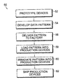
- a method of programming a radiation-hardened integrated circuit includes the steps of supplying a prototype device to a customer, having the customer develop working data patterns in the field in the same manner as a reading and writing to a normal RAM memory, having the customer save the final debugged data pattern, delivering the data pattern to the factory, loading the customer-developed data pattern into memory, programming the customer-developed data pattern into a number of production circuits, irradiating the production circuits at a total typical dosage of between 300K and 1 Meg RAD to burn the data pattern into memory, and shipping the irradiated and programmed parts to the customer.
- a second embodiment of the invention uses a programmed key including a coupled N-channel transistor and resistor, or N-channel and P-channel transistor, both coupled between the VDD power supply and ground.
- a programmed key including a coupled N-channel transistor and resistor, or N-channel and P-channel transistor, both coupled between the VDD power supply and ground.
- several programmed keys are provided. During radiation, the input node of each of the keys is set high or low and VDD is set to zero volts. During operation, the input to each of the keys is set to zero volts and VDD is turned on. The programmed keys then leak to provide a programmed output. The output node of the key remains low for those devices whose gate was previously not programmed, i.e. set to zero volts during irradiation.
- the key system can be useful for surreptitiously determining whether or a not a circuit has been irradiated above a specified value by using the output to set an internal flag, for example.
- an on-board “kill circuit” can be used to render a circuit inoperative once a specified value of radiation has been exceeded.
- the programmed and irradiated memory circuits are radiation hardened and further radiation exposure (in a radiation environment such as outer space) only further establishes or enhances the programmed memory pattern.
- FIG. 1 is a cross-sectional diagram of a prior art N-channel transistor including a substrate, N-type source/drain diffusions, a silicon dioxide gate layer, and a polysilicon gate contact;
- FIG. 2 is a cross-sectional diagram of the transistor of FIG. 1 immediately after being irradiated showing numerous electron-hole pairs in the silicon dioxide gate layer;
- FIG. 3 is a cross-sectional diagram of the transistor of FIG. 2 after electron transport, leaving numerous holes trapped in the silicon dioxide gate layer;
- FIG. 4 is a cross-sectional diagram of the transistor of FIG. 3 showing the final trapped hole charges in the silicon dioxide gate layer;
- FIG. 5 is a plot of transistor current versus gate-to-source voltage for an N-channel transistor in which the gate voltage is set to zero volts in which the transistor is irradiated at five levels of total dose radiation from 0K RADs to 1 Meg RAD;
- FIG. 6 is a plot of transistor current versus gate-to-source voltage from zero to one volt for an N-channel transistor in which the gate voltage is set to 2.7 volts in which the transistor is irradiated at five levels of total dose radiation from 50K RADs to 2 Meg RAD;
- FIG. 7 is a plot of transistor current versus gate-to-source voltage from zero to 2.5 volts for an N-channel transistor in which the gate voltage is set to 2.7 volts in which the transistor is irradiated at five levels of total dose radiation from 50K RADs to 2 Meg RAD;
- FIG. 8 is a plot of a typical SRAM cell suitable for use as a programmable memory cell according to the present invention.
- FIG. 9 is a block diagram flow chart of the method of the present invention.
- FIG. 10 is a circuit diagram of a programmable key circuit including an N-channel transistor and a resistor coupled together in a source-follower circuit configuration according to a second embodiment of the invention
- FIG. 11 is a circuit diagram of a programmable key circuit including an N-channel transistor and a resistor coupled together in a common-source amplifier configuration according to a second embodiment of the invention
- FIG. 12 is a circuit diagram of a programmable key circuit including an N-channel transistor and a P-channel transistor coupled together in a common-source amplifier configuration according to a second embodiment of the invention.
- FIG. 13 is a circuit diagram of a programmable key circuit according to any of the key circuits of FIGS. 10-12 and further including additional circuitry such as additional amplifiers or level-shifting circuitry or the like.
- FIG. 5 a plot of transistor current versus gate-to-source voltage for an N-channel transistor in which the gate voltage is set to zero volts in which the transistor is irradiated at five levels of total dose radiation from 0K RADs to 1 Meg RAD is shown. Note that for a gate voltage set to zero volts, the transistor current response is nearly identical for total dose irradiation at the zero, 100K, 200K, 300K, and 1 Meg RAD levels. The transistor exhibits a normal current response with current decreasing below VGS voltages of about 0.7 volts.
- FIG. 6 a plot of transistor current versus gate-to-source voltage from zero to one volts for an N-channel transistor in which the gate voltage is set to 2.7 volts in which the transistor is irradiated at five levels of total dose radiation from 50K RADs to 2 Meg RAD. Note that for a gate voltage set to zero volts, the transistor current response splits between a total dose of 100K RADs and 300K RADs. At dose irradiation levels of 100K RADs and below, transistor current response is similar to that of the transistor shown in FIG. 5 .
- transistor current continues (current greater than 1 ⁇ A) to persist even though VGS voltages are dropped below 0.7 volts.
- FIG. 7 a plot of transistor current versus gate-to-source voltage is expanded from zero to 2.5 volts is shown for the N-channel transistor of FIG. 6 .
- SRAM memory cell 40 includes complementary column select or data lines 26 and 32 , and row select nodes 28 and 34 .
- the core of the SRAM cell includes cross-coupled P-channel transistors 36 and 18 , and cross-coupled N-channel transistors 42 and 20 .
- the current paths of transistors 36 and 42 are coupled together at node 38 and the current paths of transistors 18 and 20 are coupled together at node 22 .
- N-channel pass transistors 24 and 30 transfer the complementary data state from circuit nodes 38 and 22 to column lines 26 and 32 , respectively.
- either of transistors 42 and 20 will have its gate biased at ground potential, and the other transistor will have its gate biased at VDD.
- the transistor having a gate biased to zero volts does not change during irradiation, but the other transistor having a gate biased at VDD experiences a voltage threshold shift.
- the voltage threshold shift causes the cross-coupled circuit shown in FIG. 8 to be permanently pre-disposed to a data state, effectively converting the normal “soft” SRAM cell into a radiation-hardened read-only memory cell (as long as the write line is kept off or low).
- FIG. 9 a block diagram 50 of the method of the present invention is shown.
- prototype soft memory devices are supplied to a customer.
- the customer uses the prototype devices in his system to develop working data patterns in the field in the same manner as a reading and writing to a normal RAM memory device.
- the final debugged data pattern is saved into memory.
- the customer delivers the data pattern to the factory so that it can be burned into equivalent commercial devices.
- the customer-developed data pattern is loaded into memory at the factory, and the customer-developed data pattern is programmed into a number of production circuits.
- the production circuits are irradiated at a typical total dosage of between 300K and 1 Meg RAD to burn the data pattern into memory as discussed above.
- a pin-compatible irradiated and programmed parts are shipped to the customer.
- a second embodiment of the programmed and irradiated N-channel transistor of the present invention is shown in FIG. 10.
- a programmed key 70 is shown including an N-channel transistor 74 and resistor 76 coupled together in a source-follower amplifier configuration.
- the main current path of key 70 flows between the VDD power supply and ground.
- the gate of key 70 is coupled to the input terminal 72 , designated KeyI.
- the junction of N-channel transistor 74 and resistor 76 forms the output node 78 labeled VO.
- the method of the present invention can be used to provide a series of programmed keys 70 , one of which is shown in FIG. 10 . During radiation, the input node of keys 70 are set high or low and VDD is set to zero volts.
- the input 72 to keys 70 are set to zero volts and VDD is turned on.
- the programmed keys leak to provide a programmed output at node 78 .
- resistor 76 is set to 2.5 Meg ⁇ , and the leakage current of N-channel is approximately one micro-amp, then the output node 78 should approach the power supply voltage of 2.5 volts (within a threshold voltage) for the previously programmed devices.
- the output node 78 remains low for those devices whose gate was previously not programmed, i.e. set to zero volts during irradiation.
- 10 can be useful for surreptitiously determining whether or a not a circuit has been irradiated above a specified value by using the output at node 78 to set an internal flag, for example.
- an on-board “kill circuit” could be used to render a circuit inoperative once a specified value of radiation has been exceeded using the output voltage signal at node 78 .
- FIGS. 11-13 illustrate alternative configurations to the programmable key circuit 70 shown in FIG. 10 according to a second embodiment of the present invention, although the output signal polarity of the circuits is inverted from key circuit 70 .
- FIG. 11 is a circuit diagram of a programmable key circuit 80 including an N-channel transistor 74 and a resistor 76 coupled together in a common-source amplifier configuration.
- FIG. 12 is a circuit diagram of a programmable key circuit 90 including an N-channel transistor 72 and a P-channel transistor 82 coupled together in a common-source amplifier configuration.
- FIG. 13 is a circuit diagram of a programmable key circuit using any of the programmable key circuits 70 , 80 , or 90 and further including additional circuitry such as additional amplifiers 100 or level-shifting circuitry 110 or the like.
Abstract
Description
Claims (2)
Priority Applications (3)
| Application Number | Priority Date | Filing Date | Title |
|---|---|---|---|
| US10/045,571 US6917533B2 (en) | 2001-10-23 | 2001-10-23 | Radiation-hardened programmable device |
| US11/132,799 US7251150B2 (en) | 2001-10-23 | 2005-05-19 | Radiation-hardened programmable device |
| US11/774,502 US7656699B2 (en) | 2001-10-23 | 2007-07-06 | Radiation-hardened programmable device |
Applications Claiming Priority (1)
| Application Number | Priority Date | Filing Date | Title |
|---|---|---|---|
| US10/045,571 US6917533B2 (en) | 2001-10-23 | 2001-10-23 | Radiation-hardened programmable device |
Related Child Applications (2)
| Application Number | Title | Priority Date | Filing Date |
|---|---|---|---|
| US11/132,799 Division US7251150B2 (en) | 2001-10-23 | 2005-05-19 | Radiation-hardened programmable device |
| US11/132,799 Continuation-In-Part US7251150B2 (en) | 2001-10-23 | 2005-05-19 | Radiation-hardened programmable device |
Publications (2)
| Publication Number | Publication Date |
|---|---|
| US20030077537A1 US20030077537A1 (en) | 2003-04-24 |
| US6917533B2 true US6917533B2 (en) | 2005-07-12 |
Family
ID=21938671
Family Applications (1)
| Application Number | Title | Priority Date | Filing Date |
|---|---|---|---|
| US10/045,571 Expired - Lifetime US6917533B2 (en) | 2001-10-23 | 2001-10-23 | Radiation-hardened programmable device |
Country Status (1)
| Country | Link |
|---|---|
| US (1) | US6917533B2 (en) |
Cited By (7)
| Publication number | Priority date | Publication date | Assignee | Title |
|---|---|---|---|---|
| US20060181905A1 (en) * | 2004-03-22 | 2006-08-17 | Summer Steven E | Radiation tolerant electrical component with non-radiation hardened FET |
| US20090108912A1 (en) * | 2007-10-24 | 2009-04-30 | Honeywell International Inc. | Circuit Architecture for Radiation Resilience |
| US8223918B2 (en) | 2006-11-21 | 2012-07-17 | Varian Medical Systems, Inc. | Radiation scanning and disabling of hazardous targets in containers |
| US8972819B2 (en) | 2011-11-22 | 2015-03-03 | Silicon Space Technology Corporation | Memory circuit incorporating radiation-hardened memory scrub engine |
| US20150062994A1 (en) * | 2013-09-04 | 2015-03-05 | Huazhong University Of Science And Technology | Radiation-hardened memory storage unit |
| US20150062995A1 (en) * | 2013-09-04 | 2015-03-05 | Huazhong University Of Science And Technology | Radiation-hardened storage unit |
| US9268637B2 (en) | 2013-03-15 | 2016-02-23 | Silicon Space Technology Corporation | Memory circuit incorporating error detection and correction (EDAC), method of operation, and system |
Citations (5)
| Publication number | Priority date | Publication date | Assignee | Title |
|---|---|---|---|---|
| US4379259A (en) * | 1980-03-12 | 1983-04-05 | National Semiconductor Corporation | Process of performing burn-in and parallel functional testing of integrated circuit memories in an environmental chamber |
| US4939694A (en) * | 1986-11-03 | 1990-07-03 | Hewlett-Packard Company | Defect tolerant self-testing self-repairing memory system |
| US5007026A (en) * | 1988-03-25 | 1991-04-09 | Sgs-Thomson Microelectronics S.A. | Method for the testing of one time programmable memories and corresponding memory |
| JPH08255843A (en) * | 1995-03-15 | 1996-10-01 | Sony Corp | Semiconductor rom device and method of writing data therein |
| US6388911B1 (en) * | 2001-03-29 | 2002-05-14 | Macronix International Co., Ltd. | Bank select structure layout of read only memory without the junction leakage |
-
2001
- 2001-10-23 US US10/045,571 patent/US6917533B2/en not_active Expired - Lifetime
Patent Citations (5)
| Publication number | Priority date | Publication date | Assignee | Title |
|---|---|---|---|---|
| US4379259A (en) * | 1980-03-12 | 1983-04-05 | National Semiconductor Corporation | Process of performing burn-in and parallel functional testing of integrated circuit memories in an environmental chamber |
| US4939694A (en) * | 1986-11-03 | 1990-07-03 | Hewlett-Packard Company | Defect tolerant self-testing self-repairing memory system |
| US5007026A (en) * | 1988-03-25 | 1991-04-09 | Sgs-Thomson Microelectronics S.A. | Method for the testing of one time programmable memories and corresponding memory |
| JPH08255843A (en) * | 1995-03-15 | 1996-10-01 | Sony Corp | Semiconductor rom device and method of writing data therein |
| US6388911B1 (en) * | 2001-03-29 | 2002-05-14 | Macronix International Co., Ltd. | Bank select structure layout of read only memory without the junction leakage |
Cited By (13)
| Publication number | Priority date | Publication date | Assignee | Title |
|---|---|---|---|---|
| US8125797B2 (en) * | 2004-03-22 | 2012-02-28 | Modular Devices, Inc. | Radiation tolerant electrical component with non-radiation hardened FET |
| US20060181905A1 (en) * | 2004-03-22 | 2006-08-17 | Summer Steven E | Radiation tolerant electrical component with non-radiation hardened FET |
| US9103925B2 (en) | 2006-11-21 | 2015-08-11 | Varian Medical Systems, Inc. | Radiation scanning and disabling of hazardous targets in containers |
| US8223918B2 (en) | 2006-11-21 | 2012-07-17 | Varian Medical Systems, Inc. | Radiation scanning and disabling of hazardous targets in containers |
| US20090108912A1 (en) * | 2007-10-24 | 2009-04-30 | Honeywell International Inc. | Circuit Architecture for Radiation Resilience |
| US7804354B2 (en) | 2007-10-24 | 2010-09-28 | Honeywell International Inc. | Circuit architecture for radiation resilience |
| US8972819B2 (en) | 2011-11-22 | 2015-03-03 | Silicon Space Technology Corporation | Memory circuit incorporating radiation-hardened memory scrub engine |
| US9201726B2 (en) | 2011-11-22 | 2015-12-01 | Silicon Space Technology Corporation | Memory circuit incorporating radiation-hardened memory scrub engine |
| US9268637B2 (en) | 2013-03-15 | 2016-02-23 | Silicon Space Technology Corporation | Memory circuit incorporating error detection and correction (EDAC), method of operation, and system |
| US20150062994A1 (en) * | 2013-09-04 | 2015-03-05 | Huazhong University Of Science And Technology | Radiation-hardened memory storage unit |
| US8995162B2 (en) * | 2013-09-04 | 2015-03-31 | Huazhong University Of Science And Technology | Radiation-hardened memory storage unit |
| US8988922B1 (en) * | 2013-09-04 | 2015-03-24 | Huazhong University Of Science And Technology | Radiation-hardened storage unit |
| US20150062995A1 (en) * | 2013-09-04 | 2015-03-05 | Huazhong University Of Science And Technology | Radiation-hardened storage unit |
Also Published As
| Publication number | Publication date |
|---|---|
| US20030077537A1 (en) | 2003-04-24 |
Similar Documents
| Publication | Publication Date | Title |
|---|---|---|
| US5406513A (en) | Mechanism for preventing radiation induced latch-up in CMOS integrated circuits | |
| US6172907B1 (en) | Silicon-oxide-nitride-oxide-semiconductor (SONOS) type memory cell and method for retaining data in the same | |
| US5111429A (en) | Single event upset hardening CMOS memory circuit | |
| Ning et al. | 1/spl mu/m MOSFET VLSI technology. IV. Hot-electron design constraints | |
| US6583470B1 (en) | Radiation tolerant back biased CMOS VLSI | |
| JP4382290B2 (en) | SEU robust circuit | |
| US8988922B1 (en) | Radiation-hardened storage unit | |
| US6275080B1 (en) | Enhanced single event upset immune latch circuit | |
| WO1999063542A1 (en) | Radiation hardened six transistor random access memory and memory device | |
| US4809226A (en) | Random access memory immune to single event upset using a T-resistor | |
| US20030189847A1 (en) | SEU resistant SRAM using feedback MOSFET | |
| US7656699B2 (en) | Radiation-hardened programmable device | |
| US6917533B2 (en) | Radiation-hardened programmable device | |
| US7199431B2 (en) | Semiconductor devices with reduced impact from alien particles | |
| Dentan et al. | Study of a CMOS-JFET-bipolar radiation hard analog-digital technology suitable for high energy physics electronics | |
| JP3185880B2 (en) | Semiconductor storage device and method of manufacturing the same | |
| Rezgui et al. | Investigation of low dose rate and bias conditions on the total dose tolerance of a CMOS flash-based FPGA | |
| Faccio | Radiation effects in the electronics for CMS | |
| Ferlet-Cavrois et al. | Comparison of the sensitivity to heavy ions of SRAM's in different SIMOX technologies | |
| US7626855B2 (en) | Semiconductor memory device | |
| Napoli et al. | CMOS/SOS 4k RAMs hardened to 100 krads (Si) | |
| US6891419B2 (en) | Methods and apparatus for employing feedback body control in cross-coupled inverters | |
| Lum et al. | Total dose hardness of field programmable gate arrays | |
| US5072133A (en) | Method and apparatus for increasing resistance of bipolar buried layer integrated circuit devices to single-event upsets | |
| Snoeys et al. | Radiation tolerance beyond 10-mrad for a pixel readout chip in standard submicron CMOS |
Legal Events
| Date | Code | Title | Description |
|---|---|---|---|
| AS | Assignment |
Owner name: AEROFLEX UTMC MICROELECTRONIC SYSTEMS, INC., COLOR Free format text: ASSIGNMENT OF ASSIGNORS INTEREST;ASSIGNORS:GARDNER, HARRY N.;KERWIN, DAVID;REEL/FRAME:012493/0178 Effective date: 20011017 |
|
| STCF | Information on status: patent grant |
Free format text: PATENTED CASE |
|
| AS | Assignment |
Owner name: GOLDMAN SACHS CREDIT PARTNERS, L.P., AS COLLATERAL Free format text: SECURITY AGREEMENT;ASSIGNOR:AEROFLEX COLORADO SPRINGS, INC., AS SUCCESSOR IN INTEREST TO AEROFLEX UTMC MICROELECTRONIC SYSTEMS, INC.;REEL/FRAME:019834/0432 Effective date: 20070815 |
|
| FPAY | Fee payment |
Year of fee payment: 4 |
|
| FEPP | Fee payment procedure |
Free format text: PAYOR NUMBER ASSIGNED (ORIGINAL EVENT CODE: ASPN); ENTITY STATUS OF PATENT OWNER: LARGE ENTITY |
|
| AS | Assignment |
Owner name: AEROFLEX COLORADO SPRINGS, INC., AS SUCCESSOR IN I Free format text: RELEASE OF SECURITY INTEREST IN INTELLECTUAL PROPERTY COLLATERAL;ASSIGNOR:GOLDMAN SACHS CREDIT PARTNERS, L.P., AS COLLATERAL AGENT;REEL/FRAME:026247/0401 Effective date: 20110509 |
|
| AS | Assignment |
Owner name: AEROFLEX COLORADO SPRINGS, INC., COLORADO Free format text: CHANGE OF NAME;ASSIGNOR:AEROFLEX UTMC MICROELECTRONIC SYSTEMS INC.;REEL/FRAME:026357/0804 Effective date: 20030829 |
|
| AS | Assignment |
Owner name: JPMORGAN CHASE BANK, NA, AS COLLATERAL AGENT, NEW Free format text: SECURITY AGREEMENT;ASSIGNORS:AEROFLEX INCORPORATED;AEROFLEX/WEINSCHEL, INC.;AEROFLEX COLORADO SPRINGS, INC.;AND OTHERS;REEL/FRAME:026422/0719 Effective date: 20110509 |
|
| FPAY | Fee payment |
Year of fee payment: 8 |
|
| AS | Assignment |
Owner name: AEROFLEX MICROELECTRONIC SOLUTIONS, INC., MICHIGAN Free format text: RELEASE OF PATENT SECURITY INTEREST;ASSIGNOR:JPMRGAN CHASE BANK, N.A.;REEL/FRAME:033728/0942 Effective date: 20140912 Owner name: AEROFLEX WICHITA, INC., KANSAS Free format text: RELEASE OF PATENT SECURITY INTEREST;ASSIGNOR:JPMRGAN CHASE BANK, N.A.;REEL/FRAME:033728/0942 Effective date: 20140912 Owner name: AEROFLEX COLORADO SPRINGS, INC., COLORADO Free format text: RELEASE OF PATENT SECURITY INTEREST;ASSIGNOR:JPMRGAN CHASE BANK, N.A.;REEL/FRAME:033728/0942 Effective date: 20140912 Owner name: AEROFLEX/WEINSCHEL, INC., MARYLAND Free format text: RELEASE OF PATENT SECURITY INTEREST;ASSIGNOR:JPMRGAN CHASE BANK, N.A.;REEL/FRAME:033728/0942 Effective date: 20140912 Owner name: AEROFLEX INCORPORATED, NEW YORK Free format text: RELEASE OF PATENT SECURITY INTEREST;ASSIGNOR:JPMRGAN CHASE BANK, N.A.;REEL/FRAME:033728/0942 Effective date: 20140912 Owner name: AEROFLEX PLAINVIEW, INC., NEW YORK Free format text: RELEASE OF PATENT SECURITY INTEREST;ASSIGNOR:JPMRGAN CHASE BANK, N.A.;REEL/FRAME:033728/0942 Effective date: 20140912 Owner name: AEROFLEX SYSTEMS GROUP, INC., CALIFORNIA Free format text: RELEASE OF PATENT SECURITY INTEREST;ASSIGNOR:JPMRGAN CHASE BANK, N.A.;REEL/FRAME:033728/0942 Effective date: 20140912 |
|
| FPAY | Fee payment |
Year of fee payment: 12 |
|
| AS | Assignment |
Owner name: COBHAM COLORADO SPRINGS INC., COLORADO Free format text: CHANGE OF NAME;ASSIGNOR:AEROFLEX COLORADO SPRINGS, INC.;REEL/FRAME:055847/0958 Effective date: 20190102 |
|
| AS | Assignment |
Owner name: CAES COLORADO SPRINGS LLC, VIRGINIA Free format text: ENTITY CONVERSION;ASSIGNOR:COBHAM COLORADO SPRINGS INC.;REEL/FRAME:061299/0532 Effective date: 20211221 Owner name: CAES COLORADO SPRINGS LLC, VIRGINIA Free format text: ENTITY CONVERSION;ASSIGNOR:COBHAM COLORADO SPRINGS INC.;REEL/FRAME:061299/0490 Effective date: 20211221 |
|
| AS | Assignment |
Owner name: JPMORGAN CHASE BANK, N.A., AS COLLATERAL AGENT, ILLINOIS Free format text: SECURITY INTEREST;ASSIGNORS:CAES COLORADO SPRINGS LLC;COBHAM ADVANCED ELECTRONIC SOLUTIONS INC.;REEL/FRAME:062337/0939 Effective date: 20230109 |