US6878565B2 - Process for improving yield of DFB lasers - Google Patents
Process for improving yield of DFB lasers Download PDFInfo
- Publication number
- US6878565B2 US6878565B2 US10/694,433 US69443303A US6878565B2 US 6878565 B2 US6878565 B2 US 6878565B2 US 69443303 A US69443303 A US 69443303A US 6878565 B2 US6878565 B2 US 6878565B2
- Authority
- US
- United States
- Prior art keywords
- laser
- facet
- grating
- lasers
- dfb
- Prior art date
- Legal status (The legal status is an assumption and is not a legal conclusion. Google has not performed a legal analysis and makes no representation as to the accuracy of the status listed.)
- Expired - Fee Related
Links
Images


Classifications
-
- H—ELECTRICITY
- H01—ELECTRIC ELEMENTS
- H01S—DEVICES USING THE PROCESS OF LIGHT AMPLIFICATION BY STIMULATED EMISSION OF RADIATION [LASER] TO AMPLIFY OR GENERATE LIGHT; DEVICES USING STIMULATED EMISSION OF ELECTROMAGNETIC RADIATION IN WAVE RANGES OTHER THAN OPTICAL
- H01S5/00—Semiconductor lasers
- H01S5/10—Construction or shape of the optical resonator, e.g. extended or external cavity, coupled cavities, bent-guide, varying width, thickness or composition of the active region
- H01S5/1082—Construction or shape of the optical resonator, e.g. extended or external cavity, coupled cavities, bent-guide, varying width, thickness or composition of the active region with a special facet structure, e.g. structured, non planar, oblique
-
- H—ELECTRICITY
- H01—ELECTRIC ELEMENTS
- H01S—DEVICES USING THE PROCESS OF LIGHT AMPLIFICATION BY STIMULATED EMISSION OF RADIATION [LASER] TO AMPLIFY OR GENERATE LIGHT; DEVICES USING STIMULATED EMISSION OF ELECTROMAGNETIC RADIATION IN WAVE RANGES OTHER THAN OPTICAL
- H01S5/00—Semiconductor lasers
- H01S5/02—Structural details or components not essential to laser action
- H01S5/028—Coatings ; Treatment of the laser facets, e.g. etching, passivation layers or reflecting layers
-
- H—ELECTRICITY
- H01—ELECTRIC ELEMENTS
- H01S—DEVICES USING THE PROCESS OF LIGHT AMPLIFICATION BY STIMULATED EMISSION OF RADIATION [LASER] TO AMPLIFY OR GENERATE LIGHT; DEVICES USING STIMULATED EMISSION OF ELECTROMAGNETIC RADIATION IN WAVE RANGES OTHER THAN OPTICAL
- H01S5/00—Semiconductor lasers
- H01S5/10—Construction or shape of the optical resonator, e.g. extended or external cavity, coupled cavities, bent-guide, varying width, thickness or composition of the active region
- H01S5/12—Construction or shape of the optical resonator, e.g. extended or external cavity, coupled cavities, bent-guide, varying width, thickness or composition of the active region the resonator having a periodic structure, e.g. in distributed feedback [DFB] lasers
-
- H—ELECTRICITY
- H01—ELECTRIC ELEMENTS
- H01S—DEVICES USING THE PROCESS OF LIGHT AMPLIFICATION BY STIMULATED EMISSION OF RADIATION [LASER] TO AMPLIFY OR GENERATE LIGHT; DEVICES USING STIMULATED EMISSION OF ELECTROMAGNETIC RADIATION IN WAVE RANGES OTHER THAN OPTICAL
- H01S5/00—Semiconductor lasers
- H01S5/0014—Measuring characteristics or properties thereof
-
- H—ELECTRICITY
- H01—ELECTRIC ELEMENTS
- H01S—DEVICES USING THE PROCESS OF LIGHT AMPLIFICATION BY STIMULATED EMISSION OF RADIATION [LASER] TO AMPLIFY OR GENERATE LIGHT; DEVICES USING STIMULATED EMISSION OF ELECTROMAGNETIC RADIATION IN WAVE RANGES OTHER THAN OPTICAL
- H01S5/00—Semiconductor lasers
- H01S5/02—Structural details or components not essential to laser action
- H01S5/0201—Separation of the wafer into individual elements, e.g. by dicing, cleaving, etching or directly during growth
-
- H—ELECTRICITY
- H01—ELECTRIC ELEMENTS
- H01S—DEVICES USING THE PROCESS OF LIGHT AMPLIFICATION BY STIMULATED EMISSION OF RADIATION [LASER] TO AMPLIFY OR GENERATE LIGHT; DEVICES USING STIMULATED EMISSION OF ELECTROMAGNETIC RADIATION IN WAVE RANGES OTHER THAN OPTICAL
- H01S5/00—Semiconductor lasers
- H01S5/10—Construction or shape of the optical resonator, e.g. extended or external cavity, coupled cavities, bent-guide, varying width, thickness or composition of the active region
- H01S5/1082—Construction or shape of the optical resonator, e.g. extended or external cavity, coupled cavities, bent-guide, varying width, thickness or composition of the active region with a special facet structure, e.g. structured, non planar, oblique
- H01S5/1085—Oblique facets
-
- H—ELECTRICITY
- H01—ELECTRIC ELEMENTS
- H01S—DEVICES USING THE PROCESS OF LIGHT AMPLIFICATION BY STIMULATED EMISSION OF RADIATION [LASER] TO AMPLIFY OR GENERATE LIGHT; DEVICES USING STIMULATED EMISSION OF ELECTROMAGNETIC RADIATION IN WAVE RANGES OTHER THAN OPTICAL
- H01S5/00—Semiconductor lasers
- H01S5/40—Arrangement of two or more semiconductor lasers, not provided for in groups H01S5/02 - H01S5/30
- H01S5/4025—Array arrangements, e.g. constituted by discrete laser diodes or laser bar
- H01S5/4087—Array arrangements, e.g. constituted by discrete laser diodes or laser bar emitting more than one wavelength
Definitions
- the present invention relates generally to Distributed Feedback (DFB) lasers, including phase-shifted DFB lasers. More particularly, the present invention is directed towards controlling the facet reflectivity of DFB lasers to improve the yield of lasers having desired characteristics.
- DFB Distributed Feedback
- DFB Distributed Feedback
- the grating strength is determined by several factors, including the grating height, grating shape, refractive index step associated with each period of the grating and the distance between the grating and the active layer.
- a coupling coefficient, ⁇ can be calculated that is indicative of the grating strength.
- the total DFB grating feedback is determined by the ⁇ L product.
- a target ⁇ L product of between about 0.5 to about 3.0 is desired.
- the target ⁇ L is within a sufficient range to achieve single mode operation over a desired laser power range. For example, for uniform gratings a ⁇ L of less than about 1.0 is commonly used whereas for a DFB laser including a phase-shifting section a ⁇ L of between 1.0 to 2.0 is commonly employed.
- a conventional DFB laser fabrication process includes forming a grating 102 on a wafer 100 .
- the grating 102 is oriented parallel to the cleavage planes containing cleaved laser bars 104 . This allows a longitudinal mode in a die to interact with the grating.
- a stripe waveguide 106 which can be, for example, a ridge waveguide or buried heterostructure, is formed perpendicular to the gratings.
- cleaved laser bars 104 commonly have an anti-reflection (AR) coating 110 formed on one of cleaved facets 112 .
- a second facet 114 can have an AR coating or a high reflectivity (HR) coating 108 formed thereon.
- a saw region 116 is shown between laser stripes 106 .
- a drawback associated with a conventional laser diode is that the reflectivity associated with facets 112 and 114 can deleteriously affect the DFB laser.
- the residual reflectivity can reduce the yield of single mode DFB lasers, particularly at high output power levels. This is due, in part, to the fact that the facet reflectivity results in the laser having Fabry-Perot cavity lasing modes that compete with the DFB lasing modes.
- AR coating such as that shown in FIG. 1B , to reduce the facet reflection to less than about 1% to suppress the Fabry-Perot modes.
- AR coatings that can be used include single layer coatings and multi-layer coatings.
- single layer AR coatings commonly have a coating that is an odd number of quarter-wavelengths thick and that has a refractive index close to the square root of the average refractive index of the laser.
- the reflectance response of a single layer AR coating is a function of wavelength and has a wavelength at which the reflectivity is a minimum and an associated bandwidth.
- the bandwidth of a single layer ultra-low reflectivity AR coating is comparatively narrow, which can make it difficult to achieve a low reflectivity at the lasing wavelength. Consequently, single layer AR coatings used in DFB lasers commonly have a reflectivity of about 1% or higher.
- a multi-layer AR coating can be used, such as multilayer coatings having quarter wavelength and half wavelength thick layers with the refractive index of each layer selected to produce a desired reflectance response.
- An advantage of a multi-layer AR coating is that the bandwidth of an ultra-low reflectivity multi-layer AR coating can be broader than a single layer ultra-low reflectivity AR coating.
- a multilayer AR coating typically requires a greater number of layers to produce a low reflectivity, increasing its cost.
- a multilayer AR coating having a low reflectivity typically requires precise control of the refractive index and thickness of each layer, resulting in large lot-to-lot variances. Also, a thick multilayer AR coating can have or induce a mechanical stress that is deleterious to the long-term reliability of the laser. As a result of the drawbacks of single-layer and multi-layer AR coatings, DFB lasers commonly have a facet reflectivity greater than 1% which results in a lower yield than desired.
- the present invention generally is a distributed feedback (DFB) laser constructed such that a laser stripe has a minimum tilt angle with respect to a cleaved facet to reduce the facet reflectivity.
- the present invention provides a method of improving the statistical yield of distributed feedback lasers by selecting a minimum tilt angle of a laser stripe with respect to a cleaved facet to reduce the facet reflectivity.
- a minimum tilt angle is selected to achieve a desired statistical yield of an optical characteristic dependent upon the effective facet reflectivity.
- the optical characteristic can be a side mode suppression ratio (SMSR), a front-to-back power ratio in phase shifted DFB lasers, or other characteristics of a laser device.
- SMSR side mode suppression ratio
- a plurality of DFB lasers having a range of tilt angles are formed, and the front facet of the lasers is coated with a single layer AR coating.
- the statistical yield of the optical characteristic is correlated with the tilt angle.
- a minimum tilt angle to achieve a desired statistical yield of DFB lasers having the desired optical characteristic is then determined.
- the number of DFB lasers tested is preferably sufficient to test over a range of grating strengths and phases at the front facet of the laser.
- Controllably reducing the residual reflectivity of DFB lasers can be used to improve the characteristics of DFB lasers used in a variety of applications.
- One application of the present invention is in phase-shifted DFB lasers, such as phase-shifted lasers including a phase-shifting section of the grating.
- Another application of the present invention can be in the manufacture/use of high power DFB lasers. Additionally, the processes described herein are compatible with a high yield manufacturing process.
- FIG. 1A is an illustration of a top view of a wafer having conventional DFB gratings and laser stripes;
- FIG. 1B is an illustration of a top view of a conventional individual cleaved DFB laser bar
- FIG. 2 is a top view illustrating a wafer with tilted laser stripes in accordance with one aspect of the present invention
- FIG. 3 is a top view of an individual laser die with a tilted laser stripe in accordance with another aspect of the present invention.
- FIG. 4 is an illustrative plot of effective facet reflectivity for a single layer coating with and without a tilted facet
- FIG. 5 is a top view of a multi-wavelength laser module with tilted laser stripes in accordance with yet another aspect of the present invention.
- FIG. 6 is a flow chart of a method of calibrating the effect of tilt angle on reflectivity
- FIG. 7 is a flow chart of a method of designing a DFB laser in accordance with yet another aspect of the present invention.
- FIG. 8 is a flow chart of a method of determining a tilt angle to improve yield of a laser characteristic in accordance with yet another aspect of the present invention.
- FIG. 9A illustrates a manufacturing design window for improving statistical yield of DFB lasers in accordance with yet another aspect of the present invention.
- FIG. 9B illustrates improvements in SMSR response versus grating strength for a decreased facet reflectivity
- FIGS. 10A and 10B show a schematic representation of a substrate and mask, respectively, having alignment marks in accordance with another aspect of the present invention.
- FIG. 11 is a flow chart of a method of forming DFB lasers in accordance with yet another aspect of the present invention.
- FIG. 2 illustrates a laser wafer 200 having laser stripes 206 oriented perpendicular to a grating 208 , such as a Bragg grating, on wafer 200 in accordance with one aspect of the present invention.
- the laser stripes 206 can be any suitable lateral waveguide structure, such as a ridge waveguide or a buried heterostructure.
- the laser stripes 206 and grating 208 are patterned to be intentionally misaligned with respect to cleavage planes 202 of wafer 200 with a selected tilt angle, ⁇ .
- Individual laser dies can be formed by cleaving laser bars and chipping the bars into individual dies. For purposes of illustration, tilt angle ⁇ in FIGS. 2 and 3 is very exaggerated and not to scale.
- FIG. 3 illustrates one such individual die 300 having a single laser stripe 306 on grating 308 .
- the grating 308 is a one-dimensional grating and is oriented at tilt angle ⁇ , with respect to cleavage planes 302 and 304 .
- the laser stripe 306 is oriented perpendicular to gratings 308 .
- the laser stripes 306 can be, for example, ridge waveguides, buried heterostructures, or other laser stripes known to one of skill in the art.
- the laser stripes 306 form an angle of incidence of ⁇ degrees with respect to a normal 314 to cleavage planes 302 , 304 (which corresponds to 90- ⁇ degrees with respect to cleavage planes 302 , 304 ).
- gratings 308 are tilted by 3 degrees with respect to cleavage plane 302 and laser stripes 306 are tilted at about 87 degrees with respect to cleavage plane 302 so that stripes 306 are approximately perpendicular to gratings 308 .
- Facet coatings 316 and 318 can be applied to facets 310 , 312 , respectively. These facet coatings 316 , 318 can generally be anti-reflection (AR) coatings designed to allow a particular wavelength of light to pass through. Preferably, the AR coatings are single layer for ease of manufacture. Examples of single layer AR coatings include single layer AR coatings of Al 2 O 3 , SiO, HfO 2 , Ta 2 O 5 , a:Si, and SiON, which should have a nominal thickness of an odd number of quarter wavelengths.
- AR anti-reflection
- Line 410 illustrates the reflectivity versus wavelength of a conventional single layer AR coating with no tilt angle.
- Line 420 illustrates the effective reflectivity versus wavelength for a laser stripe having an AR coating where the stripe is also tilted by a tilt angle.
- the tilt angle can be defined as the angle between the laser stripe and a line normal to the cleavage plane.
- the reflectivity response of a single layer AR coating 410 has a very narrow bandwidth at or below 1% reflectivity.
- a single layer AR coating can be designed to have a reflectivity of about 1%. While a reflectivity of below 1% can be achieved, the bandwidth of the reflectivity response is narrow and it is difficult to reproducibly fabricate the AR coating with the minimum reflectance centered at a desired wavelength.
- the arrows indicate a group of possible grid wavelengths, such as wavelengths within a range of ⁇ 0 ⁇ . For a laser die with a single laser stripe, variance in the refractive index of the AR coating and its thickness can result in the minimal reflectance point of the AR coating being offset from the DFB laser wavelength.
- a tilt angle of even a few degrees can reduce the effective reflectivity of a range of wavelengths by a large factor.
- ⁇ When light from a laser stripe strikes a facet at an angle, ⁇ , it is reflected from a tilted facet at an angle of 2 ⁇ with respect to the laser stripe. Only a fraction of the reflected light will couple back into the laser stripe. The fraction of reflected light that couples back into the laser stripe will depend upon the tilt angle, the laser stripe width, and other factors, such as the lateral mode shape.
- the effective reflectivity at the facet is given by the equation: ⁇ ( ⁇ ) R f ( ⁇ ) (2) where R f ( ⁇ ) is the reflectivity at the facet interface, and ⁇ ( ⁇ ) is a coupling coefficient for light reflected from the facet back into the laser stripe.
- R f ( ⁇ ) is the reflectivity at the facet interface
- ⁇ ( ⁇ ) is a coupling coefficient for light reflected from the facet back into the laser stripe.
- a conventional AR coating can be used to reduce R f ( ⁇ ).
- a single layer AR coating can be used, with the refractive index and thickness selected to achieve a low reflectivity, such as a reflectivity of about 1% or lower.
- the values of ⁇ ( ⁇ ), the refractive index, and the thickness of the AR coating can be selected for a particular angle using empirical and/or computer modeling techniques to take into account the effect of the tilt angle.
- the coupling coefficient, ⁇ ( ⁇ ) decreases as ⁇ increases.
- a tilt angle of about 5 degrees can reduce the effective facet reflectivity to less than about 1%.
- FIG. 5 illustrates a die 500 having a plurality of spaced-apart laser stripes 506 on a grating 508 .
- the grating 508 is oriented at tilt angle 520 , with respect to cleavage planes 502 and 504 .
- the separation between lasers is selected to facilitate heatsinking and provide at least partial thermal isolation of laser stripes 506 .
- the stripes 506 can, for example, be spaced apart with a center-to-center separation of several hundred microns. Alternately, the spacing can be anywhere from 50 to 2000 microns.
- each laser stripe 506 can have a Bragg grating 508 with a different grating period such that each laser stripe will have a different Bragg lasing wavelength, designated generally as ⁇ 1 , ⁇ 2 , and ⁇ n .
- Facet coatings 516 , 518 can be applied to facets 510 , 512 respectively. These facet coatings 516 , 518 can generally be AR coatings designed to allow a particular wavelength of light to pass through.
- Single layer or multilayer AR coatings are used. Examples of single layer AR coatings include single layer AR coatings of Al 2 O 3 , SiO, HfO 2 Ta 2 O 5 , a:Si, and SiON, which have a nominal thickness of an odd number of quarter wavelengths. Examples of multilayer AR coatings include alternating quarter wavelength pairs (typical number of pairs range from 1 to 6) a:Si/Ta 2 O 5 , a:Si/HfO 2 and a:Si/Al 2 O 3 .
- FIGS. 6 , 7 , and 8 are flow charts illustrating methods of acquiring data to determine desirable ranges of tilt angles.
- the effect of tilt angle on coupling coefficient and effective facet reflectivity is empirically determined.
- lasers are fabricated with a range of misalignment or tilt angles, as represented by block 602 .
- the angles can range, for example, from about 0.1 degrees to about 10 degrees.
- the lasers can be Fabry-Perot lasers formed from similar vertical epitaxially grown structures and having comparable lateral waveguides (e.g., a ridge waveguide or buried heterostructure waveguide.).
- the ridge waveguides (buried heterostructure waveguides) can have a nominal waveguide width of about 2.0 microns (0.8 microns to 1.5 microns) within a small manufacturing variance associated with a photolithography and ridge etching (buried heterostructure) process.
- lasers are tested for the range of tilt angles as represented by block 604 .
- One possible way of testing involves mounting the bars on a large metal pad that is connected to the negative terminal of a voltage or a current source.
- a probe tip contact is made to the top side of the laser (on to the bond-pad) and the probe tip is connected to the positive terminal of the aforementioned voltage or current source, thereby closing the electrical circuit and causing current to flow through the laser.
- Using a lensed fiber light is collected from the laser and is measured using a optical spectrum analyzer.
- the effective facet reflectivity can be determined.
- the calibration data can be used to generate tilt angles using the method illustrated in FIG. 7 .
- the desired maximum values of the reflectivity of the front and rear facet reflectivity are selected, as represented by block 702 .
- the front and rear facet coatings can then be chosen, as represented by block 704 . Each of the coatings will have an associated reflectivity.
- a minimum tilt angle is selected to achieve the maximum facet reflectivity, as represented by block 706 .
- FIG. 8 shows an alternate design process in which empirical data is used to determine statistical correlations between desired laser characteristics, facet coatings and tilt angles.
- multiple DFB lasers are fabricated over a selected range of tilt angles, as represented by block 802 .
- the range of tilt angles can be from about 0.1 degrees to about 10 degrees.
- DFB lasers are tested having desired facet coatings, as represented by block 804 .
- Various coatings can be used to include single layer coatings made from Al 2 O 3 , SiO, HfO 2 , Ta 2 O 5 , a:Si, and SiON and multiple layer coatings made from alternating quarter wavelength pairs (typical number of pairs range from 1 to 6) a:Si/Ta 2 O 5 , a:Si/HfO 2 and a:Si/Al 2 O 3 .
- Calibration data is generated for the effect of tilt angle and facet coating reflectivity on one or more laser characteristics, as represented by block 806 . From the calibration data, a minimum tilt angle is selected for a facet coating to form DFB lasers with desired characteristics, as represented by block 808 . These characteristics might include, for example, yield, SMSR, front-to-rear power ratio, threshold current, slope efficiency, and temperature dependence of threshold current.
- the calibration data for laser characteristics versus tilt angle and facet coating is for a selected grating process.
- the vertical epitaxial growth sequence and grating fabrication process determine the grating coupling strength.
- the distance between the grating layer to the active region, the thickness of the grating layer and the duty-cycle of the grating define the grating coupling strength.
- the cleaved length can vary by 5% and the grating coupling vary by 10% across a wafer. Consequently, the grating strength, kL, for a DFB manufacturing process has a likely range.
- the laser characteristics are also influenced by the presence of a phase-shifting section and the phase at the laser facet, which can vary between 0 and 2 ⁇ .
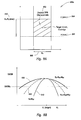
- FIG. 9A schematically represents a manufacturing design window 900 a for improving statistical yield of DFB lasers, based upon desired reflectivities and ⁇ L range.
- a desired DFB characteristic 902 to include, for example, a target ⁇ and/or ⁇ L for a given facet coating is plotted.
- a ⁇ (min) 904 , ⁇ (max) 906 , and range of ⁇ L 908 are shown for various reflectivities, R 1 , R 2 910 .
- DFB calibration data such as the side mode suppression ratio (SMSR) or front-to-rear power ratio of phase shifted DFB lasers, is collected for a statistically significant number of lasers for a given DFB laser fabrication process. The data is collected over a range of tilt angles and for at least one AR facet coating.
- SMSR side mode suppression ratio
- front-to-rear power ratio of phase shifted DFB lasers is collected for a statistically significant number of lasers for a given DFB laser fabrication process. The data is collected
- the process of collecting the calibration data over a range of tilt angles and AR facet coating(s) also corresponds to collecting calibration data over a range of ⁇ L about a target ⁇ L over a statistical range.
- the range is associated with variance in length caused by the cleavage process and variations in grating coupling, ⁇ , associated with the wafer growth and grating fabrication process.
- a target tilt angle and facet coating reflectivity 902 can be selected to achieve a desired minimum level of an attribute.
- attributes can include SMSR, front-rear power ratio, threshold current, slope efficiency, and temperature dependence of threshold current.
- calibration data can also be extended to analyze tradeoffs between tilt angle and facet coating attributes.
- FIG. 9B illustrates how appropriate selection of a minimum tilt angle can improve SMSR.
- the effect of grating strength on SMSR is illustrated assuming a fixed front and rear facet phase and rear facet reflectivity.
- the SMSR response of a conventional DFB laser with a single layer AR coating is represented by line 910 .
- This SMSR response is high for only a limited range of ⁇ L because of the deleterious effect of facet reflections on SMSR, denoted by reflectivity R 0f .
- a high SMSR implies that the laser is operating in a single mode and has a higher spectral purity. Such lasers will suffer less from the impact of fiber dispersion.
- a laser with a high SMSR (operating truly in a single mode) is needed for high-speed datacom/telecom applications where low bit-error-ratio ( ⁇ 1e ⁇ 12 ), moderately long transmission distances (typically 10's of km to 100's of km) are needed.
- Having a high SMSR over a wide range of ⁇ L allows the device designer additional level of flexibility—thereby, making feasible the simultaneous achievement of high-speed operation, low-threshold current and high-yield.
- the effective reflectivity decreases, reducing the influence of the front facet reflectivity. Consequently, the SMSR response at a tilt angle R 2f , as represented by line 920 , is significantly flatter.
- similar results can be achieved for other attributes, such as front-to-rear power ratio.
- a SMSR response can be achieved that is relatively flat.
- the SMSR response is also a target SMSR, SMSR 0 , for a statistically large fraction of lasers designed to have the target ⁇ L grating strength. Similar results can be seen by varying the phase of the front facet (which can vary from zero to 2 ⁇ ) while keeping the grating strength and the rear facet reflectivity constant. Tilting the laser facet reduces the effective reflectivity, which in turn results in a reduced dependence of SMSR on the phase of the front facet, also improving statistical yield.
- calibration data can also be acquired of multiwavelength lasers in which each laser has an attribute, such as SMSR, above a preselected level.
- multiwavelength lasers spanning a preselected wavelength range about a target laser wavelength are fabricated over a range of tilt angles to acquire calibration data.
- One or more AR facet coatings e.g., single layer AR facet coatings
- a target tilt angle and facet coating can be selected for the target grating strength. Different coatings, tilt angles, and grating strengths can be used for a given multiwavelength laser depending on the laser wavelength ⁇ 1 , ⁇ 2 , and ⁇ n .
- the DFB gratings and laser stripes can be tilted with respect to the substrate cleavage planes.
- the DFB gratings can be fabricated at an angle with respect to the cleavage planes using a variety of methods.
- some e-beam lithography systems used to pattern gratings include mechanical and/or electronic systems or devices to rotate the e-beam pattern relative to an alignment feature on the wafer (e.g., a cleaved edge or alignment mark).
- a custom wafer chuck such as a wedge-edged wafer chuck, can be used to increase the wafer rotation of an e-beam system.
- FIGS. 10A and 10B One exemplary embodiment of the alignment features are shown in FIGS. 10A and 10B .
- a system 1000 shows a pair of alignment marks 1010 formed on a substrate 1002 , such as the wafer discussed above. These alignment marks 1010 , and corresponding alignment marks 1012 on a mask 1050 (FIG. 10 B), can be used to align mask 1050 having laser bar (waveguide) outlines 1030 with DFB gratings 1020 on substrate 1002 .
- One advantage of system 1000 is that, when the two sets of alignment marks 1010 , 1012 are correctly aligned, laser bar outlines 1030 are perpendicular to grating 1020 located on substrate 1002 . This allows laser bars to then be formed in approximate positions corresponding to laser bar outlines 1030 at a tilt angle with respect to cleavage plane 1040 , according to exemplary embodiments of the present invention.
- a significant tilt angle can alter the etch properties of plane-selective wet chemical etches used to define ridges in a ridge-waveguide or buried heterostructure fabrication process. Consequently, a substantially isotropic ridge fabrication can be used.
- ridges can be formed using a dry etching process such as reactive ion etching, by a combination of dry and wet etching, or by selecting a wet chemical etch that is not significantly affected by the tilt.
- a wet chemical etch might be, for example a mixture of Bromine, Hydrogen-per-oxide and water.
- FIG. 11 is a flow chart depicting the steps involved in one exemplary DFB fabrication process using a ridge waveguide laser.
- An initial epitaxial growth is performed on a wafer, as represented by block 1102 .
- the growing process can use, for example, metal-organic chemical vapor deposition (MOCVD), molecular beam epitaxy (MBE), or other epitaxial growth processes.
- MOCVD metal-organic chemical vapor deposition
- MBE molecular beam epitaxy
- the base epitaxial growth can include an active layer, spacer layer, and a grating layer into which the grating is to be formed.
- the nominal grating strength and laser length is selected for a nominal ⁇ L of between about 1 to 3.
- a grating is defined or patterned at the desired tilt angle, as represented by block 1104 .
- e-beam lithography is used to pattern an e-beam sensitive resist into a grating at the desired tilt angle, which is then transferred into the semiconductor grating layer using a dry etch process.
- Desired tilt angles can be anywhere from about 0.1 degrees to about 10 degrees.
- the grating layer is overgrown in a second epitaxial growth step (e.g., using MOCVD or MBE) to form a planar DFB laser wafer, as represented by block 1106 .
- a laser stripe is then formed by etching each ridge with its long axis perpendicular to the gratings and tilted with respect to the surface normal of the cleavage plane, as represented by block 1108 .
- the ridges are etched to a preselected depth using reactive ion etching. An additional shallow wet chemical etch can be performed to remove residual surface damage.
- Conventional photolithographic alignment processes, as described above, have an alignment accuracy to within about 0.1°.
- a p-contact is then deposited onto a portion of the ridge waveguide, as represented by block 1110 .
- the substrate is thinned using a combination of chemical and mechanical process, as represented by block 1112 .
- the n-contact is then deposited onto the substrate, as represented by block 1114 .
- the contacts are then fixed using rapid thermal annealing, as represented by block 1116 .
- the lasers are then cleaved into bars, as represented by block 1118 , using conventional fabrication techniques.
- the facets are coated and the bars diced into devices, as represented by blocks 1120 and 1122 , respectively.
- One possible method of coating involves loading the bars into a holder which is then placed inside a e-beam evaporator with the facet that needs to be coated facing the source.
- the source consists of a crucible containing a charge which we wish to coat on to the facet (eg: a:Si).
- the chamber is then pumped down to low vacuum.
- the source is then evaporated on to the facet using an electron beam. After facet coating, the bars are then carefully unloaded to a sticky tape.
- a dicing tool (containing a sharp pointed tip) is used to scribe/delineate the dies. This is followed by application of a gentle force along the edges of the die to facilitate singulation into individual dies.
- Controllably reducing the residual reflectivity of DFB lasers can be used to improve the characteristics of DFB lasers used in a variety of applications.
- One application of the present invention is in phase-shifted DFB lasers, such as phase-shifted lasers including a phase-shifting section of the grating.
- Phase-shifted DFB lasers are particularly sensitive to residual facet reflections. Consequently, the present invention can be used to improve the yield of phase-shifted DFB lasers having a phase-shifting section.
- Another application of the present invention can be in the manufacture/use of high power DFB lasers At high power levels the optical gain along the length of the laser can vary due to the interaction of the optical profile with the active region. Reducing the facet reflectivity improves the yield of high power lasers having acceptable SMSR. Reducing the facet reflectivity can also be used to improve the front/rear facet power ratio of phase-shifted DFB lasers.
- the processes described herein are compatible with a high yield manufacturing process.
- the front and rear facets can be formed using a conventional bar cleaving process. This facilitates a high yield facet coating process.
- the present invention requires only minor modifications to standard DFB lasers processing, making it compatible with a low cost manufacturing process.
- calibration data is formed for a particular DFB laser process, such as one using a standard lateral waveguide strength, bar length, and grating characteristics, the same tilt angle can be used in subsequent manufacturing runs.
Abstract
Description
λDFB=2n eq Λ/m (1)
where m is the grating order, neq is the average refractive index, and Λ is the grating period.
β(θ)R f(θ) (2)
where Rf(θ) is the reflectivity at the facet interface, and β(θ) is a coupling coefficient for light reflected from the facet back into the laser stripe. A conventional AR coating can be used to reduce Rf(θ).
Claims (34)
Priority Applications (1)
| Application Number | Priority Date | Filing Date | Title |
|---|---|---|---|
| US10/694,433 US6878565B2 (en) | 2002-10-28 | 2003-10-27 | Process for improving yield of DFB lasers |
Applications Claiming Priority (2)
| Application Number | Priority Date | Filing Date | Title |
|---|---|---|---|
| US42206802P | 2002-10-28 | 2002-10-28 | |
| US10/694,433 US6878565B2 (en) | 2002-10-28 | 2003-10-27 | Process for improving yield of DFB lasers |
Publications (2)
| Publication Number | Publication Date |
|---|---|
| US20040131099A1 US20040131099A1 (en) | 2004-07-08 |
| US6878565B2 true US6878565B2 (en) | 2005-04-12 |
Family
ID=32685111
Family Applications (1)
| Application Number | Title | Priority Date | Filing Date |
|---|---|---|---|
| US10/694,433 Expired - Fee Related US6878565B2 (en) | 2002-10-28 | 2003-10-27 | Process for improving yield of DFB lasers |
Country Status (1)
| Country | Link |
|---|---|
| US (1) | US6878565B2 (en) |
Cited By (2)
| Publication number | Priority date | Publication date | Assignee | Title |
|---|---|---|---|---|
| US20080147172A1 (en) * | 1993-09-30 | 2008-06-19 | White Geoffrey H | Intraluminal Graft |
| US8927306B2 (en) | 2013-02-28 | 2015-01-06 | Avago Technologies General Ip (Singapore) Pte. Ltd. | Etched-facet lasers having windows with single-layer optical coatings |
Families Citing this family (5)
| Publication number | Priority date | Publication date | Assignee | Title |
|---|---|---|---|---|
| US6885793B2 (en) * | 2003-06-10 | 2005-04-26 | Spectra Physics, Inc | Cleaving laser diode bars having gratings |
| TWI250706B (en) * | 2005-02-24 | 2006-03-01 | Gigacomm Corppration | Optical communication module and multimode distributed feedback laser diode |
| CN100444482C (en) * | 2006-03-09 | 2008-12-17 | 南京大学 | Method and device for making the semiconductor laser based on reconstruction-equivalent chirp technology |
| WO2020181497A1 (en) * | 2019-03-12 | 2020-09-17 | 华为技术有限公司 | Double-cavity dfb laser chip, optical emission component, optical module, and optical network device |
| US11949453B2 (en) * | 2021-06-25 | 2024-04-02 | Electronics And Telecommunications Research Institute | Test device and test method for DFB-LD for RoF system |
Citations (2)
| Publication number | Priority date | Publication date | Assignee | Title |
|---|---|---|---|---|
| US20020131465A1 (en) * | 2001-02-01 | 2002-09-19 | Lo Yu-Hwa | Integrated surface-emitting laser and modulator device |
| US20030169787A1 (en) * | 2002-03-07 | 2003-09-11 | Igor Vurgaftman | Photonic-crystal distributed-feedback and distributed bragg-reflector lasers |
-
2003
- 2003-10-27 US US10/694,433 patent/US6878565B2/en not_active Expired - Fee Related
Patent Citations (2)
| Publication number | Priority date | Publication date | Assignee | Title |
|---|---|---|---|---|
| US20020131465A1 (en) * | 2001-02-01 | 2002-09-19 | Lo Yu-Hwa | Integrated surface-emitting laser and modulator device |
| US20030169787A1 (en) * | 2002-03-07 | 2003-09-11 | Igor Vurgaftman | Photonic-crystal distributed-feedback and distributed bragg-reflector lasers |
Non-Patent Citations (1)
| Title |
|---|
| "Reflection Loss of Laser Mode From Tilted End Mirror," by Dietrich Marcuse, IEEE Journal of Lightwave Technology, vol. 7, No. 2, Feb. 1989. |
Cited By (2)
| Publication number | Priority date | Publication date | Assignee | Title |
|---|---|---|---|---|
| US20080147172A1 (en) * | 1993-09-30 | 2008-06-19 | White Geoffrey H | Intraluminal Graft |
| US8927306B2 (en) | 2013-02-28 | 2015-01-06 | Avago Technologies General Ip (Singapore) Pte. Ltd. | Etched-facet lasers having windows with single-layer optical coatings |
Also Published As
| Publication number | Publication date |
|---|---|
| US20040131099A1 (en) | 2004-07-08 |
Similar Documents
| Publication | Publication Date | Title |
|---|---|---|
| US6292503B1 (en) | Ridge type semiconductor laser of laterally-coupled distributed feedback and method of manufacturing the same | |
| JP6220864B2 (en) | Laser with improved beam shape | |
| Fricke et al. | 980-nm DBR lasers using higher order gratings defined by i-line lithography | |
| US8306086B2 (en) | Algainn-based lasers produced using etched facet technology | |
| AU3099500A (en) | Vertical cavity surface emitting lasers with consistent slope efficiencies | |
| US20070047609A1 (en) | Wafer testing of edge emitting lasers | |
| US6878565B2 (en) | Process for improving yield of DFB lasers | |
| US7542497B2 (en) | AlGaInN-based lasers with dovetailed ridge | |
| Vaissié et al. | High efficiency surface-emitting laser with subwavelength antireflection structure | |
| US6865195B2 (en) | Edge-emitting semiconductor tunable laser | |
| US20020159491A1 (en) | Surface emitting laser | |
| JP2001168456A (en) | Gain combination/distribution feedback type semiconductor laser | |
| Scherer et al. | High reflectivity dielectric mirror deposition by reactive magnetron sputtering | |
| EP1540732B1 (en) | Fabry-perot laser with wavelength control | |
| Robadey et al. | Gain coupled DFB lasers with active layer grown on a corrugated substrate by molecular beam epitaxy | |
| CN114944594A (en) | Laser device with non-absorbing mirror and method | |
| JPH07122814A (en) | Semiconductor laser and its manufacture | |
| WO2003007443A1 (en) | Manufacturing semiconductor lasers having gratings | |
| JP5264764B2 (en) | Etched facet ridge laser with etch stop | |
| JPH1126869A (en) | Method for measuring cod level of semiconductor laser element and method for evaluating semiconductor laser element | |
| Corvini et al. | Performance and reliability of high-power 670-690 nm CW laser diode bars grown by solid source molecular beam epitaxy | |
| Hofstetter et al. | Characterization of InGaN/GaN-based multi-quantum well distributed feedback lasers | |
| JPH09321382A (en) | Laser beam source and application thereof | |
| Kellermann et al. | Wavelength-graded horizontal cavity laser array with postgrowth adjustment of wavelength | |
| Vettiger et al. | FULL-WAFER TECHNOLOGY FOR LARGE-SCALE LASER FABRICATION |
Legal Events
| Date | Code | Title | Description |
|---|---|---|---|
| AS | Assignment |
Owner name: FINISAR CORPORATION, CALIFORNIA Free format text: ASSIGNMENT OF ASSIGNORS INTEREST;ASSIGNOR:THIYAGARAJAN, SUMESH MANI K.;REEL/FRAME:015041/0565 Effective date: 20040228 |
|
| FPAY | Fee payment |
Year of fee payment: 4 |
|
| FPAY | Fee payment |
Year of fee payment: 8 |
|
| REMI | Maintenance fee reminder mailed | ||
| LAPS | Lapse for failure to pay maintenance fees | ||
| STCH | Information on status: patent discontinuation |
Free format text: PATENT EXPIRED DUE TO NONPAYMENT OF MAINTENANCE FEES UNDER 37 CFR 1.362 |
|
| FP | Lapsed due to failure to pay maintenance fee |
Effective date: 20170412 |
|
| AS | Assignment |
Owner name: II-VI DELAWARE, INC., DELAWARE Free format text: ASSIGNMENT OF ASSIGNORS INTEREST;ASSIGNOR:FINISAR CORPORATION;REEL/FRAME:052286/0001 Effective date: 20190924 |