US6870777B2 - Semiconductor memory device having self-timing circuit - Google Patents
Semiconductor memory device having self-timing circuit Download PDFInfo
- Publication number
- US6870777B2 US6870777B2 US10/103,017 US10301702A US6870777B2 US 6870777 B2 US6870777 B2 US 6870777B2 US 10301702 A US10301702 A US 10301702A US 6870777 B2 US6870777 B2 US 6870777B2
- Authority
- US
- United States
- Prior art keywords
- dummy
- circuit
- memory cell
- path
- decoder
- Prior art date
- Legal status (The legal status is an assumption and is not a legal conclusion. Google has not performed a legal analysis and makes no representation as to the accuracy of the status listed.)
- Expired - Fee Related
Links
- 239000004065 semiconductor Substances 0.000 title claims abstract description 31
- 239000000872 buffer Substances 0.000 claims description 34
- 230000004044 response Effects 0.000 claims description 7
- 230000000644 propagated effect Effects 0.000 claims 1
- 230000004913 activation Effects 0.000 description 10
- 238000010586 diagram Methods 0.000 description 8
- 239000000047 product Substances 0.000 description 6
- 239000006227 byproduct Substances 0.000 description 4
- 230000001934 delay Effects 0.000 description 4
- 238000005516 engineering process Methods 0.000 description 2
- 230000009467 reduction Effects 0.000 description 2
- 230000003213 activating effect Effects 0.000 description 1
- 230000003247 decreasing effect Effects 0.000 description 1
- 230000000694 effects Effects 0.000 description 1
- 238000004519 manufacturing process Methods 0.000 description 1
- 238000000034 method Methods 0.000 description 1
- 230000004048 modification Effects 0.000 description 1
- 238000012986 modification Methods 0.000 description 1
- 230000003071 parasitic effect Effects 0.000 description 1
Images


Classifications
-
- G—PHYSICS
- G11—INFORMATION STORAGE
- G11C—STATIC STORES
- G11C7/00—Arrangements for writing information into, or reading information out from, a digital store
- G11C7/22—Read-write [R-W] timing or clocking circuits; Read-write [R-W] control signal generators or management
- G11C7/227—Timing of memory operations based on dummy memory elements or replica circuits
-
- G—PHYSICS
- G11—INFORMATION STORAGE
- G11C—STATIC STORES
- G11C7/00—Arrangements for writing information into, or reading information out from, a digital store
- G11C7/24—Memory cell safety or protection circuits, e.g. arrangements for preventing inadvertent reading or writing; Status cells; Test cells
-
- G—PHYSICS
- G11—INFORMATION STORAGE
- G11C—STATIC STORES
- G11C7/00—Arrangements for writing information into, or reading information out from, a digital store
- G11C7/22—Read-write [R-W] timing or clocking circuits; Read-write [R-W] control signal generators or management
-
- G—PHYSICS
- G11—INFORMATION STORAGE
- G11C—STATIC STORES
- G11C8/00—Arrangements for selecting an address in a digital store
- G11C8/18—Address timing or clocking circuits; Address control signal generation or management, e.g. for row address strobe [RAS] or column address strobe [CAS] signals
Definitions
- the present invention generally relates to semiconductor memory devices, and particularly relates to a semiconductor memory device equipped with a timing control circuit that simulates signal delay.
- timing control signals that define the operation timing of internal circuitry are generated from external signals by use of delay circuits or the like.
- the timing of timing control signals generated in this manner may deviate if parasitic load capacitance or resistance associated with wires exhibits variation due to the product variation. Timing settings must thus be made with a sufficient margin by taking into account such deviations, which is a factor that hinders effort toward the attainment of high-speed semiconductor memory devices.
- timing control circuit In order to obviate this problem, some types of semiconductor memory devices simulate signal delay inside the semiconductor memory devices, thereby generate accurate timing control signals.
- Such timing control circuit is called a self-timing circuit. For example, the path that incurs the longest timing delay at the time of memory access is taken into consideration, and a circuit is provided to simulate the signal delay along this path, thereby generating timing control signals for defining the operation timing of internal circuitry.
- the timing control signal has timing that emulates actual memory access, so that timing deviation caused by the product variation can be suppressed to some extent.
- the path that incurs the longest timing delay used for generating the timing control signal is a path that is farthest away from the input/output circuit, and that accesses the memory cell that is farthest away from the word decoder.
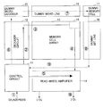
- FIG. 1 is an illustrative drawing for explaining timing compensation when the path farthest away from an input/output circuit and a word decoder is used.
- the semiconductor memory device of FIG. 1 includes a control circuit 11 , a decoder circuit 12 , a memory cell array 13 , a read-write amplifier 14 , a dummy word decoder 15 , a dummy word line 16 , a dummy memory cell 17 , and a dummy bit line 18 .
- the decoder circuit 12 selectively activates a word line of the memory cell array 13 in response to a clock signal CK and an address signal ADDRESS supplied to the control circuit 11 from an exterior of the device, thereby supplying a read signal to a memory cell 19 .
- a signal path along which the read signal propagates is shown as signal paths P 1 , P 2 and P 3 .
- the memory cell 19 that is accessed in the memory cell array 13 is shown as a cell that is farthest away from the control circuit 11 .
- Data read from the memory cell 19 is supplied to the read-write amplifier 14 through a path p 4 that corresponds to bit lines of the memory cell array 13 .
- the data retrieval paths P 1 , P 2 , P 3 , and P 4 together form the path that incurs the longest delay for a data read operation, and is thus a critical path that is most critical in terms of timing.
- the dummy word decoder 15 activates the dummy word line 16 based on the clock signal CK and the address signal ADDRESS supplied to the control circuit 11 from the exterior of the device, thereby supplying a read signal to the dummy memory cell 17 .
- a path along which this read signal propagates is shown as paths P 1 , P 6 , and P 7 .
- a dummy-memory-cell signal read from the dummy memory cell 17 is supplied through the dummy bit line 18 to the control circuit 11 .
- the control circuit 11 supplies a sense amplifier activation signal to the read-write amplifier 14 so as to amplify the real data that is read.
- the path along which the dummy-memory-cell signal and the sense amplifier activation signal propagate is shown as paths P 8 , P 9 , and P 5 .
- the real data that is read through the data retrieval paths P 1 , P 2 , P 3 , and P 4 is amplified by the read-write amplifier 14 and then output to the exterior of the device through a path P 10 .
- the path along which the dummy-memory-cell signal is retrieved has a timing delay longer than that of the critical path that has the longest timing delay in the memory cell array 13 . This insures that the reading of data along the critical path is properly performed.
- the self-timing circuit generates a timing control signal (i.e., the sense amplifier activation signal) that simulates real memory access, thereby canceling a timing deviation caused by product variation.
- the dummy memory cell 17 is provided farther away than the memory cell 19 that is farthest away from the control circuit 11 . Accordingly, the load of driving the dummy word decoder 15 , the dummy word line 16 , the dummy bit line 18 , etc., is greater than the maximum load that can be incurred when reading data from the memory cell array 13 . This gives rise to a problem in that power consumption by the self-timing circuit increases. The power consumption by the self-timing circuit is not an ignorable size in memory devices for which a reduction of power consumption is a primary consideration.
- a semiconductor memory device includes a data access path for accessing a memory cell, a signal drive circuit which drives a signal on said data access path, a dummy path that emulates said data access path, and a dummy drive circuit which emulates said signal drive circuit, wherein said dummy path has a smaller load than said data access path, and said dummy drive circuit has a smaller drive capacity than said signal drive circuit.
- the semiconductor memory device as described above drives the dummy path having a smaller lard than the actual data access path by use of the dummy drive circuit having a smaller drive capacity than the actual signal drive circuit. This makes it possible to achieve a circuit configuration that consumes a less electric power than the related-art self-timing circuit, yet achieves timing control that cancels timing deviations caused by product variation.
- a dummy word decoder, a dummy word line circuit, a dummy memory cell, and a dummy bit line circuit are situated at a corner of the memory cell array closest to the decoder circuit and the input/output circuit.
- the dummy word line circuit includes a dummy word line that extends in the same direction as word lines of the memory cell array, and is folded to make a U-turn.
- the dummy bit line circuit includes dummy bit lines that extend in the same direction as the bit lines of the memory cell array, and are folded to make a U-turn.
- the dummy path for emulating the data access path can be implemented as a relatively short path.
- a semiconductor memory device includes a self-timing circuit which emulates data access to a memory cell so as to generate a timing control signal, the self-timing circuit using a dummy path having a relatively small load compared with a circuit that is emulated, and driving the dummy path by a drive capacity that is proportionately small.
- the semiconductor memory device as described above employs the dummy path having a relatively small load compared with a circuit that is emulated, and drives the dummy path by a drive capacity that is proportionately small, thereby making it possible to achieve a circuit configuration that consumes a less electric power than the related-art self-timing circuit, yet achieving timing control that cancels timing deviations caused by product variation.
- FIG. 1 is an illustrative drawing for explaining a related-art timing compensation when a path farthest away from an input/output circuit and a word decoder is used;
- FIG. 2 is a diagram showing a configuration of a semiconductor memory device provided with a self-timing circuit according to the present invention
- FIG. 3 is an enlarged view of signal propagation paths of a dummy word decoder, a dummy word line circuit, a dummy memory cell, and a dummy bit line circuit;
- FIG. 4 is a circuit diagram for explaining the setting of a dummy load and a buffer drive capacity in a decoder circuit and the dummy word decoder;
- FIG. 5 is a circuit diagram for explaining the setting of a dummy load and a buffer drive capacity with respect to word lines of a memory cell array and a dummy word line of the dummy word line circuit;
- FIG. 6 is a circuit diagram for explaining the setting of a dummy load and a buffer drive capacity with respect to bit lines of the memory cell array and dummy bit lines of the dummy bit line circuit.
- FIG. 2 is a diagram showing a configuration of a semiconductor memory device provided with a self-timing circuit according to the present invention.
- the semiconductor memory device of FIG. 2 includes the control circuit 11 , the decoder circuit 12 , the memory cell array 13 , the read-write amplifier 14 , a dummy word decoder 25 , a dummy word line circuit 26 , a dummy memory cell 27 , and a dummy bit line circuit 28 .
- the dummy word decoder 25 , the dummy word line circuit 26 , the dummy memory cell 27 , and the dummy bit line circuit 28 together constitute a self-timing circuit of the present invention.
- the dummy word decoder 25 of this self-timing circuit is situated at a position closer to the control circuit 11 than the decoder circuit 12 .
- the dummy word line circuit 26 , the dummy memory cell 27 , and the dummy bit line circuit 28 are positioned closer to the control circuit 11 than the memory cell array 13 .
- the decoder circuit 12 selectively activates a word line of the memory cell array 13 in response to a clock signal CK and an address signal ADDRESS supplied to the control circuit 11 from an exterior of the device, thereby supplying a read signal to the memory cell 19 .
- a signal path along which the read signal propagates is shown as signal paths P 1 , P 2 and P 3 .
- the memory cell 19 that is accessed in the memory cell array 13 is shown as a cell that is farthest away from the control circuit 11 .
- Data read from the memory cell 19 is supplied to the read-write amplifier 14 through a path p 4 that corresponds to bit lines of the memory cell array 13 .
- the data retrieval paths P 1 , P 2 , P 3 , and P 4 together form the path that incurs the longest delay for a data read operation, and is thus a critical path that is most critical in terms of timing.
- the control circuit 11 controls the dummy word decoder 25 situated closer to the control circuit 11 than the decoder circuit 12 .
- the dummy word decoder 25 activates a dummy word line of the dummy word line circuit 26 that extends in the same direction as word lines of the memory cell array 13 and is folded to make a U-turn, thereby supplying a read signal to the dummy memory cell 27 .
- a path along which this read signal propagates is shown as paths P 1 , P 6 , and P 7 .
- a dummy-memory-cell signal read from the dummy memory cell 27 is supplied to the control circuit 11 through dummy bit lines of the dummy bit line circuit 28 that extends in the same direction as the bit lines of the memory cell array 13 and is folded to make a U-turn. Based on this dummy-memory-cell signal, the control circuit 11 supplies a sense amplifier activation signal to the read-write amplifier 14 so as to amplify the real data that is read.
- the path along which the dummy-memory-cell signal and the sense amplifier activation signal propagate is shown as paths P 8 , P 9 , and P 5 .
- the real data that is read through the data retrieval paths P 1 , P 2 , P 3 , and P 4 is amplified by the read-write amplifier 14 and then output to the exterior of the device through a path P 10 .
- FIG. 3 is an enlarged view of signal propagation paths of the dummy word decoder 25 , the dummy word line circuit 26 , the dummy memory cell 27 , and the dummy bit line circuit 28 .
- the control circuit 11 is provided with a buffer 30 , which supplies a signal to drive a dummy decode line 31 of the dummy word decoder 25 .
- the dummy decode line 31 is folded to make a U-turn, and is connected to a buffer 32 at the end of the return path. In this manner, the signal from the buffer 30 is supplied to the buffer 32 .
- the buffer 32 drives a dummy word line 33 of the dummy word line circuit 26 .
- the dummy word line 33 makes a U-turn as shown in FIG. 3 , and is connected to the dummy memory cell 27 at the end of the return path.
- Activation of the dummy word line 33 results in a cell signal being read from the dummy memory cell 27 , and this cell signal is supplied to a buffer 35 through a dummy bit line 34 of the dummy bit line circuit 28 .
- the dummy bit line 34 is folded to make a U-turn as shown in FIG. 3 .
- the configuration of the present invention uses a circuit arrangement as shown in FIG. 2 and FIG. 3 , and folds the dummy decode line 31 , the dummy word line 33 , and the dummy bit line 34 to make a U-turn, thereby making it possible to provide the self-timing circuit at a corner of the memory cell array 13 in the proximity of the control circuit 11 .
- the load of each dummy circuit and the drive capacity of buffers that drive the respective dummy circuits are properly adjusted in the dummy word decoder 25 , the dummy word line circuit 26 , and the dummy bit line circuit 28 , thereby achieving proper time delays.
- This aspect will be described in the following.
- FIG. 4 is a circuit diagram for explaining the setting of a dummy load and a buffer drive capacity in the decoder circuit 12 and the dummy word decoder 25 .
- the decoder circuit 12 for actual data reading and data writing includes NAND circuits 41 through 44 and inverters 45 through 48 , for example.
- Four decoded signal lines S 1 through S 4 are connected to the NAND circuits 41 through 44 , respectively.
- One of these signal lines is set to HIGH to select one of the word lines WL 1 through WL 4 that extend inside the memory cell array 13 .
- a buffer 30 A of the control circuit 11 drives a decode line 49 to drive the NAND circuits so as to activate the selected word line at proper timing.
- the dummy word decoder 25 includes a NAND circuit 51 and an inverter 32 (which is the same as the buffer 32 of FIG. 3 ).
- the NAND circuit 51 has the same circuitry structure as the NAND circuits 41 through 44
- the inverter 32 has the same circuitry structure as the inverters 45 through 48 .
- the buffer 30 of the control circuit 11 activates the dummy decode line 31 .
- the NAND circuit 51 is thus driven at proper timing, thereby activating the dummy word line 33 at proper timing.
- the drive capacity of the buffer 30 is set equal to a quarter of the drive capacity of the buffer 30 A, for example.
- the wire load of the dummy decode line 31 is set to a quarter of the wire load of the decode line 49 .
- the dummy decode line 31 is connected to the load that is equal in amount to one word
- the decode line 49 is connected to the load that is equal in amount to four words.
- a delay from a node X to a node Y through the buffer 30 A and the decode line 49 will be equal to the delay from the node X to a node YY through the buffer 30 and the dummy decode line 31 .
- the node Y corresponds to the critical path that has the longest delay among all the data read paths.
- FIG. 5 is a circuit diagram for explaining the setting of a dummy load and a buffer drive capacity with respect to word lines of the memory cell array 13 and the dummy word line 33 of the dummy word line circuit 26 .
- the memory cell array 13 includes a word line WL 1 and a plurality of memory cells 61 - 1 through 61 -n.
- the memory cells 61 - 1 through 61 -n are connected to the word line WL.
- Selective activation of the word line WL 1 allows access to be made to the memory cells 61 - 1 through 61 -n through bit lines.
- the total number n of the memory cells 61 - 1 through 61 -n may be equal to 256, for example.
- the word line WL corresponds to the critical path, and is driven by the inverter 45 of the decoder circuit 12 (see FIG. 4 ).
- the dummy word line circuit 26 includes the dummy word line 33 and a plurality of dummy memory cells 62 - 1 through 62 -m- 1 .
- the dummy word line 33 is connected to the dummy memory cells 62 - 1 through 62 -m- 1 , and is further connected to the dummy memory cell 27 .
- the dummy word line 33 thus has a total of m dummy memory cells connected thereto.
- the number m of the dummy memory cells may be 16, for example.
- the dummy word line 33 is driven by the inverter 32 of the dummy word decoder 25 .
- the drive capacity of the inverter 32 is set to one sixteenth of the drive capacity of the inverter 45 , for example, and the wire load of the dummy word line 33 is set to one sixteenth of the wire load of the word line WL 1 .
- the dummy word line 33 has the 16 dummy memory cells connected thereto as loads, and the word line WL 1 has the 256 memory cells connected thereto.
- the dummy load of the dummy word line circuit 26 is one sixteenth of the load of the word line WL 1 .
- a delay from the node Y to a node Z through the inverter 45 and the word line WL 1 becomes the same as the delay from the node YY to a node ZZ through the inverter 32 and the dummy word line 33 .
- the node Z corresponds to the critical path that has the longest delay among all the data read paths.
- FIG. 6 is a circuit diagram for explaining the setting of a dummy load and a buffer drive capacity with respect to bit lines of the memory cell array 13 and the dummy bit line 34 of the dummy bit line circuit 28 .
- the memory cell array 13 includes bit lines BL and /BL and a plurality of memory cells 71 - 1 through 71 -k.
- the memory cell 71 - 1 is the same as the memory cell 61 -n that belongs to the critical path among the memory cells selected by the word line WL 1 in FIG. 5 .
- the memory cells 71 - 1 through 71 -k are connected to the bit lines BL and /BL, and data of the selected memory cell 71 - 1 is transferred to the read-write amplifier 14 through the bit lines BL and /BL.
- the number k of the memory cells 71 - 1 through 71 -k may be 256, for example.
- the dummy bit line circuit 28 includes a pair of dummy bit lines 34 and a plurality of dummy memory cells 72 - 1 through 72 - 1 - 1 .
- the dummy bit lines 34 is connected to the dummy memory cells 72 - 1 through 72 - 1 - 1 , and is further connected to the dummy memory cell 27 . Accordingly, the dummy bit lines 34 has the total number 1 of dummy memory cells connected thereto.
- the number 1 of the dummy memory cell is 16, for example.
- the dummy bit lines 34 carry the dummy data (dummy-memory-cell signals) of the dummy memory cell 27 , and supplies it to the buffer 35 shown in FIG. 3 .
- the buffer 35 may be an inverter, and serves as a dummy sense amplifier to amplify the received signal, followed by supplying the amplified signal to the control circuit 11 .
- the wire load of the dummy bit lines 34 is set to one sixteenth of the wire load of the bit lines BL and /BL.
- the dummy bit lines 34 has the 16 dummy memory cells connected thereto as loads, and the bit lines BL and /BL has the 256 dummy memory cells attached thereto.
- the data read from the dummy memory cell 27 has an amplitude on the dummy bit lines 34 that is one sixteenth of the amplitude of the data read from the memory cell 71 - 1 appearing on the bit lines BL and /BL.
- the signals on the dummy bit lines 34 are amplified by the buffer 35 serving as a dummy sense amplifier, and are supplied to the control circuit 11 .
- the control circuit 11 generates a sense amplifier activation signal to activate the sense amplifiers of the read-write amplifier 14 .
- the sense amplifier activation signal serves as a timing control signal that defines timing by simulating actual memory access, thereby making it possible to cancel timing deviation caused by product variation in a reliable manner.
- the self-timing circuit is provided at the corner of the memory cell array that is closest to the word decoder and the read-write amplifier, and has a reduced size with decreased dummy loads. Further, the capacity of buffers that drive the dummy circuits is reduced in proportion to the reduction of the dummy loads. This makes it possible to achieve a circuit configuration that consumes a less electric power than the related-art self-timing circuit, yet achieves timing control that cancels timing deviations caused by the product variation.
- delays of buffers with no load thereon needs to be taken into consideration like the buffers 30 and 30 A shown in FIG. 4 , for example. Delays without loads typically depend on the gate length regardless of the gate width if transistors of the same technology are used. Use of transistors having the same gate length, therefore, insures that the delays of buffers with no load thereon are set identical to each other.
- wire resistance also needs to be taken into consideration in addition to wire capacitance.
- the basic unit of a capacitance load is the wire capacitance of one memory cell plus the gate capacitance, so that a ratio of the wire capacitance load to the entire capacitance load is constant regardless of the number of memory cells.
- the effect of wire resistance on the entire delay is constant irrespective of the number of memory cells. Because of this reason, it suffices to take into account only the capacitance load.
Abstract
Description
Claims (8)
Applications Claiming Priority (2)
| Application Number | Priority Date | Filing Date | Title |
|---|---|---|---|
| JP2001-182067 | 2001-06-15 | ||
| JP2001182067A JP4894095B2 (en) | 2001-06-15 | 2001-06-15 | Semiconductor memory device |
Publications (2)
| Publication Number | Publication Date |
|---|---|
| US20020191446A1 US20020191446A1 (en) | 2002-12-19 |
| US6870777B2 true US6870777B2 (en) | 2005-03-22 |
Family
ID=19022232
Family Applications (1)
| Application Number | Title | Priority Date | Filing Date |
|---|---|---|---|
| US10/103,017 Expired - Fee Related US6870777B2 (en) | 2001-06-15 | 2002-03-22 | Semiconductor memory device having self-timing circuit |
Country Status (4)
| Country | Link |
|---|---|
| US (1) | US6870777B2 (en) |
| JP (1) | JP4894095B2 (en) |
| KR (1) | KR100735642B1 (en) |
| TW (1) | TW563131B (en) |
Cited By (8)
| Publication number | Priority date | Publication date | Assignee | Title |
|---|---|---|---|---|
| US20050099864A1 (en) * | 2003-11-12 | 2005-05-12 | Brown Jeffrey S. | Metal programmable self-timed memories |
| US20060279986A1 (en) * | 2005-05-30 | 2006-12-14 | Seiichi Suzuki | Semiconductor device and programming method therefor |
| US20080008020A1 (en) * | 2006-07-05 | 2008-01-10 | Stmicroelectronics Sa | Memory device with programmable control for activation of read amplifiers |
| US20090327620A1 (en) * | 2008-06-27 | 2009-12-31 | Igor Arsovski | Circuit structure and method for digital integrated circuit performance screening |
| US20110044095A1 (en) * | 2005-07-21 | 2011-02-24 | Renesas Technology Corp. | Semiconductor memory device |
| US20120147687A1 (en) * | 2010-12-13 | 2012-06-14 | Kabushiki Kaisha Toshiba | Semiconductor memory device |
| US8804438B2 (en) | 2012-08-04 | 2014-08-12 | Freescale Semiconductor, Inc. | Memory device |
| US9047936B2 (en) | 2012-05-29 | 2015-06-02 | Lsi Corporation | Memory device having control circuitry for write tracking using feedback-based controller |
Families Citing this family (4)
| Publication number | Priority date | Publication date | Assignee | Title |
|---|---|---|---|---|
| US7483327B2 (en) * | 2006-03-02 | 2009-01-27 | Freescale Semiconductor, Inc. | Apparatus and method for adjusting an operating parameter of an integrated circuit |
| JP4805698B2 (en) * | 2006-03-13 | 2011-11-02 | 株式会社東芝 | Semiconductor memory device |
| US9418716B1 (en) * | 2015-04-15 | 2016-08-16 | Qualcomm Incorporated | Word line and bit line tracking across diverse power domains |
| US9858988B1 (en) * | 2016-07-08 | 2018-01-02 | Qualcomm Incorporated | Timing circuit for memories |
Citations (19)
| Publication number | Priority date | Publication date | Assignee | Title |
|---|---|---|---|---|
| US4939693A (en) * | 1989-02-14 | 1990-07-03 | Texas Instruments Incorporated | BiCMOS static memory with improved performance stability |
| US5018111A (en) * | 1988-12-27 | 1991-05-21 | Intel Corporation | Timing circuit for memory employing reset function |
| US5440515A (en) * | 1994-03-08 | 1995-08-08 | Motorola Inc. | Delay locked loop for detecting the phase difference of two signals having different frequencies |
| US5473568A (en) * | 1993-08-09 | 1995-12-05 | Nec Corporation | Read write memory with negative feedback-controlled dummy memory circuit |
| US5596539A (en) * | 1995-12-28 | 1997-01-21 | Lsi Logic Corporation | Method and apparatus for a low power self-timed memory control system |
| US5608681A (en) * | 1996-01-22 | 1997-03-04 | Lsi Logic Corporation | Fast memory sense system |
| US5694369A (en) * | 1995-03-31 | 1997-12-02 | Nec Corporation | Semiconductor memory device |
| US5732035A (en) * | 1990-06-14 | 1998-03-24 | Creative Integrated Systems, Inc. | Very large scale integrated planar read only memory |
| US5742552A (en) * | 1996-10-31 | 1998-04-21 | Texas Instruments Incorporated | Timing control for clocked sense amplifiers |
| US6194932B1 (en) * | 1997-10-20 | 2001-02-27 | Fujitsu Limited | Integrated circuit device |
| US6198689B1 (en) * | 1998-11-27 | 2001-03-06 | Fujitsu Limited | Integrated circuit device with built-in self timing control circuit |
| US6239635B1 (en) * | 1998-07-06 | 2001-05-29 | Fujitsu Limited | Self-timing control circuit |
| US6246622B1 (en) * | 1999-07-30 | 2001-06-12 | Nec Corporation | Semiconductor memory device |
| US6285604B1 (en) * | 2000-01-06 | 2001-09-04 | Taiwan Semiconductor Manufacturing Co., Ltd. | Dummy memory cells for high accuracy self-timing circuits in dual-port SRAM |
| US6288950B1 (en) * | 1999-09-14 | 2001-09-11 | Nec Corporation | Semiconductor memory device capable of generating offset voltage independent of bit line voltage |
| US6295241B1 (en) * | 1987-03-30 | 2001-09-25 | Kabushiki Kaisha Toshiba | Dynamic random access memory device |
| US20020015333A1 (en) * | 2000-08-07 | 2002-02-07 | Fujitsu Limited | Semiconductor memory device |
| US6529436B1 (en) * | 2001-04-26 | 2003-03-04 | Lsi Logic Corporation | Supply degradation compensation for memory self time circuits |
| US6643204B1 (en) * | 2001-05-16 | 2003-11-04 | Lsi Logic Corporation | Self-time scheme to reduce cycle time for memories |
Family Cites Families (7)
| Publication number | Priority date | Publication date | Assignee | Title |
|---|---|---|---|---|
| US4926387A (en) * | 1988-12-27 | 1990-05-15 | Intel Corporation | Memory timing circuit employing scaled-down models of bit lines using reduced number of memory cells |
| JPH02201797A (en) * | 1989-01-31 | 1990-08-09 | Toshiba Corp | Semiconductor memory device |
| JPH07272484A (en) * | 1994-03-25 | 1995-10-20 | Nippon Telegr & Teleph Corp <Ntt> | Semiconductor memory |
| KR100228525B1 (en) * | 1996-10-09 | 1999-11-01 | 윤종용 | Method for sensing bit-line using dummy cell |
| US5790560A (en) * | 1996-12-13 | 1998-08-04 | International Business Machines Corporation | Apparatus and method for timing self-timed circuitry |
| US5841720A (en) * | 1997-08-26 | 1998-11-24 | International Business Machines Corporation | Folded dummy world line |
| US5999482A (en) * | 1997-10-24 | 1999-12-07 | Artisan Components, Inc. | High speed memory self-timing circuitry and methods for implementing the same |
-
2001
- 2001-06-15 JP JP2001182067A patent/JP4894095B2/en not_active Expired - Fee Related
-
2002
- 2002-03-22 US US10/103,017 patent/US6870777B2/en not_active Expired - Fee Related
- 2002-03-22 TW TW091105627A patent/TW563131B/en not_active IP Right Cessation
- 2002-04-16 KR KR1020020020577A patent/KR100735642B1/en not_active IP Right Cessation
Patent Citations (19)
| Publication number | Priority date | Publication date | Assignee | Title |
|---|---|---|---|---|
| US6295241B1 (en) * | 1987-03-30 | 2001-09-25 | Kabushiki Kaisha Toshiba | Dynamic random access memory device |
| US5018111A (en) * | 1988-12-27 | 1991-05-21 | Intel Corporation | Timing circuit for memory employing reset function |
| US4939693A (en) * | 1989-02-14 | 1990-07-03 | Texas Instruments Incorporated | BiCMOS static memory with improved performance stability |
| US5732035A (en) * | 1990-06-14 | 1998-03-24 | Creative Integrated Systems, Inc. | Very large scale integrated planar read only memory |
| US5473568A (en) * | 1993-08-09 | 1995-12-05 | Nec Corporation | Read write memory with negative feedback-controlled dummy memory circuit |
| US5440515A (en) * | 1994-03-08 | 1995-08-08 | Motorola Inc. | Delay locked loop for detecting the phase difference of two signals having different frequencies |
| US5694369A (en) * | 1995-03-31 | 1997-12-02 | Nec Corporation | Semiconductor memory device |
| US5596539A (en) * | 1995-12-28 | 1997-01-21 | Lsi Logic Corporation | Method and apparatus for a low power self-timed memory control system |
| US5608681A (en) * | 1996-01-22 | 1997-03-04 | Lsi Logic Corporation | Fast memory sense system |
| US5742552A (en) * | 1996-10-31 | 1998-04-21 | Texas Instruments Incorporated | Timing control for clocked sense amplifiers |
| US6194932B1 (en) * | 1997-10-20 | 2001-02-27 | Fujitsu Limited | Integrated circuit device |
| US6239635B1 (en) * | 1998-07-06 | 2001-05-29 | Fujitsu Limited | Self-timing control circuit |
| US6198689B1 (en) * | 1998-11-27 | 2001-03-06 | Fujitsu Limited | Integrated circuit device with built-in self timing control circuit |
| US6246622B1 (en) * | 1999-07-30 | 2001-06-12 | Nec Corporation | Semiconductor memory device |
| US6288950B1 (en) * | 1999-09-14 | 2001-09-11 | Nec Corporation | Semiconductor memory device capable of generating offset voltage independent of bit line voltage |
| US6285604B1 (en) * | 2000-01-06 | 2001-09-04 | Taiwan Semiconductor Manufacturing Co., Ltd. | Dummy memory cells for high accuracy self-timing circuits in dual-port SRAM |
| US20020015333A1 (en) * | 2000-08-07 | 2002-02-07 | Fujitsu Limited | Semiconductor memory device |
| US6529436B1 (en) * | 2001-04-26 | 2003-03-04 | Lsi Logic Corporation | Supply degradation compensation for memory self time circuits |
| US6643204B1 (en) * | 2001-05-16 | 2003-11-04 | Lsi Logic Corporation | Self-time scheme to reduce cycle time for memories |
Cited By (16)
| Publication number | Priority date | Publication date | Assignee | Title |
|---|---|---|---|---|
| US7746722B2 (en) * | 2003-11-12 | 2010-06-29 | Lsi Corporation | Metal programmable self-timed memories |
| US7400543B2 (en) * | 2003-11-12 | 2008-07-15 | Lsi Logic Corporation | Metal programmable self-timed memories |
| US20050099864A1 (en) * | 2003-11-12 | 2005-05-12 | Brown Jeffrey S. | Metal programmable self-timed memories |
| US20080253206A1 (en) * | 2003-11-12 | 2008-10-16 | Jeffrey Scott Brown | Metal programmable self-timed memories |
| US20060279986A1 (en) * | 2005-05-30 | 2006-12-14 | Seiichi Suzuki | Semiconductor device and programming method therefor |
| US7376033B2 (en) | 2005-05-30 | 2008-05-20 | Spansion Llc | Semiconductor device and programming method therefor |
| US8130581B2 (en) | 2005-07-21 | 2012-03-06 | Renesas Electronics Corporation | Semiconductor memory device |
| US20110044095A1 (en) * | 2005-07-21 | 2011-02-24 | Renesas Technology Corp. | Semiconductor memory device |
| US7623400B2 (en) * | 2006-07-05 | 2009-11-24 | Stmicroelectronics, Sa | Memory device with programmable control for activation of read amplifiers |
| US20080008020A1 (en) * | 2006-07-05 | 2008-01-10 | Stmicroelectronics Sa | Memory device with programmable control for activation of read amplifiers |
| US20090327620A1 (en) * | 2008-06-27 | 2009-12-31 | Igor Arsovski | Circuit structure and method for digital integrated circuit performance screening |
| US8214699B2 (en) | 2008-06-27 | 2012-07-03 | International Business Machines Corporation | Circuit structure and method for digital integrated circuit performance screening |
| US20120147687A1 (en) * | 2010-12-13 | 2012-06-14 | Kabushiki Kaisha Toshiba | Semiconductor memory device |
| US8630135B2 (en) * | 2010-12-13 | 2014-01-14 | Kabushiki Kaisha Toshiba | Semiconductor memory device |
| US9047936B2 (en) | 2012-05-29 | 2015-06-02 | Lsi Corporation | Memory device having control circuitry for write tracking using feedback-based controller |
| US8804438B2 (en) | 2012-08-04 | 2014-08-12 | Freescale Semiconductor, Inc. | Memory device |
Also Published As
| Publication number | Publication date |
|---|---|
| KR100735642B1 (en) | 2007-07-06 |
| JP2003007055A (en) | 2003-01-10 |
| JP4894095B2 (en) | 2012-03-07 |
| KR20020096866A (en) | 2002-12-31 |
| US20020191446A1 (en) | 2002-12-19 |
| TW563131B (en) | 2003-11-21 |
Similar Documents
| Publication | Publication Date | Title |
|---|---|---|
| US6798711B2 (en) | Memory with address management | |
| US6260128B1 (en) | Semiconductor memory device which operates in synchronism with a clock signal | |
| US6870777B2 (en) | Semiconductor memory device having self-timing circuit | |
| KR0154586B1 (en) | Semiconductor memory device | |
| US6538473B2 (en) | High speed digital signal buffer and method | |
| US6055208A (en) | Method and circuit for sending a signal in a semiconductor device during a setup time | |
| KR100669131B1 (en) | Semiconductor memory device | |
| JPH06162784A (en) | Semiconductor integrated circuit device | |
| US5886936A (en) | Memory cell data line equalization controlling circuit for semiconductor memory device | |
| US4992983A (en) | Semiconductor memory device with an improved write control circuit | |
| JP2002076879A (en) | Semiconductor device | |
| US5953739A (en) | Synchronous DRAM cache using write signal to determine single or burst write | |
| US6026496A (en) | Method and apparatus for generating a pulse | |
| US6678193B2 (en) | Apparatus and method for tracking between data and echo clock | |
| JPH052888A (en) | Memory cell circuit for gate array | |
| KR970004816B1 (en) | A semiconductor memory device containing an address transition detection circuit | |
| US6909664B1 (en) | Semiconductor memory device with simplified control of column switches | |
| KR100190099B1 (en) | Data line equalization circuit | |
| KR100247906B1 (en) | Data processing method | |
| JP2001101864A (en) | Synchronous semiconductor memory | |
| JP2001067875A (en) | Output circuit | |
| JPH1125675A (en) | Semiconductor storage device | |
| KR19980014990A (en) | A column path circuit diagram using a secondary sense amplifier of a semiconductor memory device | |
| KR20030060175A (en) | A semiconductor memory device with a high speed through an improved bit line developing | |
| JPH10188563A (en) | Semiconductor memory circuit |
Legal Events
| Date | Code | Title | Description |
|---|---|---|---|
| AS | Assignment |
Owner name: FUJITSU LIMITED, JAPAN Free format text: ASSIGNMENT OF ASSIGNORS INTEREST;ASSIGNOR:MAKI, YASUHIKO;REEL/FRAME:012715/0793 Effective date: 20020315 |
|
| FEPP | Fee payment procedure |
Free format text: PAYOR NUMBER ASSIGNED (ORIGINAL EVENT CODE: ASPN); ENTITY STATUS OF PATENT OWNER: LARGE ENTITY |
|
| FPAY | Fee payment |
Year of fee payment: 4 |
|
| AS | Assignment |
Owner name: FUJITSU MICROELECTRONICS LIMITED, JAPAN Free format text: ASSIGNMENT OF ASSIGNORS INTEREST;ASSIGNOR:FUJITSU LIMITED;REEL/FRAME:021998/0645 Effective date: 20081104 Owner name: FUJITSU MICROELECTRONICS LIMITED,JAPAN Free format text: ASSIGNMENT OF ASSIGNORS INTEREST;ASSIGNOR:FUJITSU LIMITED;REEL/FRAME:021998/0645 Effective date: 20081104 |
|
| AS | Assignment |
Owner name: FUJITSU SEMICONDUCTOR LIMITED, JAPAN Free format text: CHANGE OF NAME;ASSIGNOR:FUJITSU MICROELECTRONICS LIMITED;REEL/FRAME:024982/0245 Effective date: 20100401 |
|
| FPAY | Fee payment |
Year of fee payment: 8 |
|
| AS | Assignment |
Owner name: SOCIONEXT INC., JAPAN Free format text: ASSIGNMENT OF ASSIGNORS INTEREST;ASSIGNOR:FUJITSU SEMICONDUCTOR LIMITED;REEL/FRAME:035507/0851 Effective date: 20150302 |
|
| REMI | Maintenance fee reminder mailed | ||
| LAPS | Lapse for failure to pay maintenance fees | ||
| STCH | Information on status: patent discontinuation |
Free format text: PATENT EXPIRED DUE TO NONPAYMENT OF MAINTENANCE FEES UNDER 37 CFR 1.362 |
|
| FP | Lapsed due to failure to pay maintenance fee |
Effective date: 20170322 |