US6849294B2 - Method for fabricating circuit pattern of printed circuit board - Google Patents
Method for fabricating circuit pattern of printed circuit board Download PDFInfo
- Publication number
- US6849294B2 US6849294B2 US10/456,565 US45656503A US6849294B2 US 6849294 B2 US6849294 B2 US 6849294B2 US 45656503 A US45656503 A US 45656503A US 6849294 B2 US6849294 B2 US 6849294B2
- Authority
- US
- United States
- Prior art keywords
- metal plated
- forming
- plated layer
- insulation material
- layers
- Prior art date
- Legal status (The legal status is an assumption and is not a legal conclusion. Google has not performed a legal analysis and makes no representation as to the accuracy of the status listed.)
- Expired - Fee Related
Links
Images


Classifications
-
- H—ELECTRICITY
- H05—ELECTRIC TECHNIQUES NOT OTHERWISE PROVIDED FOR
- H05K—PRINTED CIRCUITS; CASINGS OR CONSTRUCTIONAL DETAILS OF ELECTRIC APPARATUS; MANUFACTURE OF ASSEMBLAGES OF ELECTRICAL COMPONENTS
- H05K3/00—Apparatus or processes for manufacturing printed circuits
- H05K3/02—Apparatus or processes for manufacturing printed circuits in which the conductive material is applied to the surface of the insulating support and is thereafter removed from such areas of the surface which are not intended for current conducting or shielding
-
- H—ELECTRICITY
- H05—ELECTRIC TECHNIQUES NOT OTHERWISE PROVIDED FOR
- H05K—PRINTED CIRCUITS; CASINGS OR CONSTRUCTIONAL DETAILS OF ELECTRIC APPARATUS; MANUFACTURE OF ASSEMBLAGES OF ELECTRICAL COMPONENTS
- H05K3/00—Apparatus or processes for manufacturing printed circuits
- H05K3/22—Secondary treatment of printed circuits
- H05K3/24—Reinforcing the conductive pattern
- H05K3/243—Reinforcing the conductive pattern characterised by selective plating, e.g. for finish plating of pads
-
- C—CHEMISTRY; METALLURGY
- C25—ELECTROLYTIC OR ELECTROPHORETIC PROCESSES; APPARATUS THEREFOR
- C25D—PROCESSES FOR THE ELECTROLYTIC OR ELECTROPHORETIC PRODUCTION OF COATINGS; ELECTROFORMING; APPARATUS THEREFOR
- C25D5/00—Electroplating characterised by the process; Pretreatment or after-treatment of workpieces
- C25D5/02—Electroplating of selected surface areas
- C25D5/022—Electroplating of selected surface areas using masking means
-
- H—ELECTRICITY
- H05—ELECTRIC TECHNIQUES NOT OTHERWISE PROVIDED FOR
- H05K—PRINTED CIRCUITS; CASINGS OR CONSTRUCTIONAL DETAILS OF ELECTRIC APPARATUS; MANUFACTURE OF ASSEMBLAGES OF ELECTRICAL COMPONENTS
- H05K3/00—Apparatus or processes for manufacturing printed circuits
- H05K3/02—Apparatus or processes for manufacturing printed circuits in which the conductive material is applied to the surface of the insulating support and is thereafter removed from such areas of the surface which are not intended for current conducting or shielding
- H05K3/04—Apparatus or processes for manufacturing printed circuits in which the conductive material is applied to the surface of the insulating support and is thereafter removed from such areas of the surface which are not intended for current conducting or shielding the conductive material being removed mechanically, e.g. by punching
- H05K3/045—Apparatus or processes for manufacturing printed circuits in which the conductive material is applied to the surface of the insulating support and is thereafter removed from such areas of the surface which are not intended for current conducting or shielding the conductive material being removed mechanically, e.g. by punching by making a conductive layer having a relief pattern, followed by abrading of the raised portions
-
- H—ELECTRICITY
- H05—ELECTRIC TECHNIQUES NOT OTHERWISE PROVIDED FOR
- H05K—PRINTED CIRCUITS; CASINGS OR CONSTRUCTIONAL DETAILS OF ELECTRIC APPARATUS; MANUFACTURE OF ASSEMBLAGES OF ELECTRICAL COMPONENTS
- H05K2201/00—Indexing scheme relating to printed circuits covered by H05K1/00
- H05K2201/03—Conductive materials
- H05K2201/0332—Structure of the conductor
- H05K2201/0364—Conductor shape
- H05K2201/0376—Flush conductors, i.e. flush with the surface of the printed circuit
-
- H—ELECTRICITY
- H05—ELECTRIC TECHNIQUES NOT OTHERWISE PROVIDED FOR
- H05K—PRINTED CIRCUITS; CASINGS OR CONSTRUCTIONAL DETAILS OF ELECTRIC APPARATUS; MANUFACTURE OF ASSEMBLAGES OF ELECTRICAL COMPONENTS
- H05K2201/00—Indexing scheme relating to printed circuits covered by H05K1/00
- H05K2201/09—Shape and layout
- H05K2201/09009—Substrate related
- H05K2201/09036—Recesses or grooves in insulating substrate
-
- H—ELECTRICITY
- H05—ELECTRIC TECHNIQUES NOT OTHERWISE PROVIDED FOR
- H05K—PRINTED CIRCUITS; CASINGS OR CONSTRUCTIONAL DETAILS OF ELECTRIC APPARATUS; MANUFACTURE OF ASSEMBLAGES OF ELECTRICAL COMPONENTS
- H05K3/00—Apparatus or processes for manufacturing printed circuits
- H05K3/10—Apparatus or processes for manufacturing printed circuits in which conductive material is applied to the insulating support in such a manner as to form the desired conductive pattern
- H05K3/107—Apparatus or processes for manufacturing printed circuits in which conductive material is applied to the insulating support in such a manner as to form the desired conductive pattern by filling grooves in the support with conductive material
-
- H—ELECTRICITY
- H05—ELECTRIC TECHNIQUES NOT OTHERWISE PROVIDED FOR
- H05K—PRINTED CIRCUITS; CASINGS OR CONSTRUCTIONAL DETAILS OF ELECTRIC APPARATUS; MANUFACTURE OF ASSEMBLAGES OF ELECTRICAL COMPONENTS
- H05K3/00—Apparatus or processes for manufacturing printed circuits
- H05K3/22—Secondary treatment of printed circuits
- H05K3/28—Applying non-metallic protective coatings
-
- H—ELECTRICITY
- H05—ELECTRIC TECHNIQUES NOT OTHERWISE PROVIDED FOR
- H05K—PRINTED CIRCUITS; CASINGS OR CONSTRUCTIONAL DETAILS OF ELECTRIC APPARATUS; MANUFACTURE OF ASSEMBLAGES OF ELECTRICAL COMPONENTS
- H05K3/00—Apparatus or processes for manufacturing printed circuits
- H05K3/40—Forming printed elements for providing electric connections to or between printed circuits
- H05K3/42—Plated through-holes or plated via connections
- H05K3/425—Plated through-holes or plated via connections characterised by the sequence of steps for plating the through-holes or via connections in relation to the conductive pattern
- H05K3/426—Plated through-holes or plated via connections characterised by the sequence of steps for plating the through-holes or via connections in relation to the conductive pattern initial plating of through-holes in substrates without metal
Definitions
- the present invention relates to a printed circuit board and, more particularly, to a method for fabricating a circuit pattern of a printed circuit board that is capable of easily forming a fine pitch circuit pattern and improving a reliability.
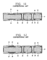
- FIGS. 1A to 1 J are sequential process of a method for fabricating a circuit pattern of a printed circuit board in accordance with a conventional art.
- a base material 10 is prepared.
- the base material 10 is formed by coating a copper foil 16 at both sides of an insulation material 12 with a predetermined thickness.
- a plurality of through holes 18 are formed in the base material 10 .
- the through holes 18 serve as a path for electrically connecting the copper foil coated at both sides of the insulation material 12 , and as such it can be formed with various sizes and as many as desired according to a circuit design.
- a copper plated layer 20 is formed at a surface of the base material 10 . That is, the copper plated layer 20 is formed also at the inner surface of the through holes 18 as well as at the surface of the copper foil 16 , electrically connecting the copper foil 16 formed at both sides of the insulation material 12 .
- an etching resist 22 is coated at the surface of the copper plated layer 20 , which is then exposed.
- the exposing process is performed such that an exposing mask 26 with a plurality of openings 24 is positioned at both surfaces of the base material 10 with the etching resist 22 coated thereon, on which ultraviolet ray is irradiated, so that the ultraviolet ray is partially irradiated at the etching resist 22 through the openings 24 formed at the exposing mask 26 .
- a development process proceeds to remove the etching resist 22 of the exposed portion. That is, the etching resist at the portion to which ultraviolet ray has been irradiated is removed to expose the copper plated layer 20 , while the etching resist 22 without ultraviolet irradiated thereto as being covered by the exposed mask 26 remains, not exposing the copper plated layer 20 .
- an etching process proceeds to remove the exposed copper plated layer 20 and the copper foil 16 .
- the remaining etching resist 22 is removed. Then, the copper plated layer 20 remaining at both surfaces of the insulation 12 by being protected by the etching resist 22 and the copper foil 16 form a circuit patterns 28 .
- a resin is plugged in the through hole 18 and regions between the circuit patterns 28 to form a resin layer 30 .
- a photoresist 34 is coated at a surface of the resin layer 30 .
- some of the circuit patterns 28 are used as a connection pad 32 for electrical connection with outside and the photoresist 34 is not coated at the circuit pattern used as the connection pad 32 .
- circuit patterns 28 are formed by the copper foil 16 and the copper plated layer 20 at both surfaces of the insulation material 12 , and electrically connected to each other by the copper plated layer 20 coated at the inner surface of the through holes 18 .
- a gold-plated layer 36 is formed on the portion of the connection pad 32 for connection to other electronic parts.
- the gold-plated layer 36 serves to ensure a firm attachment when a gold wire is connected to the connection pad 32 or a solder ball is formed on the connection pad 32 .
- FIG. 2 is a partial perspective view of the printed circuit board in accordance with the conventional art
- FIG. 3 is a sectional view showing the connection pad 32 with the gold plated layer 36 formed thereon in accordance with the conventional art.
- the printed circuit board in accordance with the conventional art has a structure that the circuit patterns 28 are formed at the surface of the insulation layer 12 , on which the photoresist 34 is coated, and the gold plated layer 36 is formed at the connection pad 32 , where no photoresist 34 is coated, for connecting with other electronic parts.
- a printed circuit board such as a flip chip package or a chip scale package (CSP) having almost the same size as the semiconductor chip is in demand increasingly, and the connection pad is in the tendency of sharply increase in number as the semiconductor chip is of high density. Accordingly, in order to form more circuit patterns in the same area for a signal transmission with the semiconductor chip, the width and the thickness of the circuit pattern is reduced and a space between circuit patterns becomes fine.
- CSP chip scale package
- an etching solution permeates from the upper portion of the connection pad 32 to its lower portion, so that the upper portion of the connection pad is more removed than the lower portion as the upper portion is exposed by the etching solution longer time than the lower portion, leaving a trapezoid shape.
- a fine circuit pattern 28 or a connection pad 32 in terms of thickness and width.
- the surface flatness is degraded due to the existence of the protruded circuit pattern 28 and the connection pad 32 , resulting in a high possibility that the solder resist 30 may be cracked due to a thermal impact, and when a semiconductor chip is molded at the printed circuit board, a flow of the molding compound is not good.
- connection pad 32 Third, as shown in FIG. 3 , the upper surface and the left and right surfaces of the connection pad 32 are exposed on which the copper plated layer 20 and the gold-plated layer 36 are formed.
- the gold-plated region is relatively enlarged and the gold-plated layer 36 is formed long in the downward direction of both sides of the connection pad 32 , causing much problem for insulation between the adjacent connection pads.
- the thickness of the copper plated layer 20 and the gold plated layer 36 formed at the side makes it difficult to obtain a fine pitch.
- an object of the present invention is to provide a method for fabricating a printed circuit board capable of easily forming a fine circuit pattern.
- Another object of the present invention is to provide a method for fabricating a printed circuit board capable of considerably reducing deficiency occurrence by improving a surface flatness of a printed circuit board and reducing a molding gap in a molding operation after a chip is mounted.
- Still another object of the present invention is to provide a method for fabricating a printed circuit board capable of minimizing a gold plated area by forming a gold plated layer only at an upper surface of a connection pad and obtaining a fine pitch between connection pads.
- a circuit pattern fabrication method of a printed circuit board including: a first step of forming a resin layer at a surface of an insulation material; a second step of selectively removing the resin layer; a third step of forming a metal plated layer at the surface of the resin layer-removed portion of the insulation material to form circuit patterns and a connection pad; and a fourth step of forming a gold plated layer on the connection pad.
- the metal plated layer is formed by a copper plating.
- the third step includes: forming a metal plated layer at a surface of the insulation material and at a surface of the remaining resin layer; removing the metal plated layer formed at the surface of the resin layer; and coating a solder resist at a surface of other portion than the portion where the connection pad is formed.
- the metal plated layer formed at the surface of the resin layer is removed by abrasion, and the resin layer and the metal plated layer are leveled through the abrasion process.
- connection pad is formed in a rectangular shape without having a difference in width between a bottom portion attached at the insulation material and the upper portion.
- the gold-plated layer is formed only at the upper surface of the connection pad.
- a method for fabricating a circuit pattern of a printed circuit board including: a first step of preparing an insulation material having a plurality of through holes; a second step of forming a resin layer at both surfaces of the insulation material; a third step of selectively removing the resin layer and forming a metal plated layer at both surfaces of the insulation material where the resin layer has been removed to form circuit patterns and a connection pad, and forming a metal plated layer inside the through hole to electrically connect the circuit patterns existing at both sides; and a fourth step of forming a gold plated layer on the connection pad.
- a method for fabricating a circuit pattern of a printed circuit board including: a first step of forming a resin layer at a surface of an insulation material; a second step of selectively removing the resin layer to form a plurality of grooves; a third step of forming a metal plated layer on the groove to form circuit patterns and a connection pad; a fourth step of forming a gold plated layer at a surface of the connection pad; and a fifth step of removing the gold plated layer protruded from the surface of the resin layer.
- the third step includes: forming a metal plated layer inside the groove and at the surface of the resin layer; and removing the metal plated layer formed at the surface of the resin layer to form a connection pad and circuit patterns.
- the metal plated layer formed at the surface of the resin layer is removed by abrasion.
- connection pad is formed with a thickness not higher than a depth of the groove, and an edge of the connection pad is protruded upwardly so as to be attached at the inner surface of the groove.
- the resin layer is abraded to a certain thickness in order to remove the gold plated layer protruded from the resin layer and flatten the surface of the resin layer.
- FIGS. 1A to 1 J are a sequential process of a method for fabricating a circuit pattern of a printed circuit board in accordance with a conventional art
- FIG. 2 is a partial perspective view showing a printed circuit board in accordance with the conventional art
- FIG. 3 is a sectional view taken along line III—III of FIG. 2 ;
- FIGS. 4A to 4 H are a sequential process of a method for fabricating a circuit pattern of a printed circuit board in accordance with a first embodiment of the present invention
- FIG. 5 is a partial perspective view showing a printed circuit board in accordance with the first embodiment of the present invention.
- FIG. 6 is a sectional view taken along line VI—VI of FIG. 5 ;
- FIGS. 7A to 7 E are a sequential process of a method for fabricating a circuit pattern of a printed circuit board in accordance with a second embodiment of the present invention.
- FIGS. 4A to 4 H are a sequential process of a method for fabricating a circuit pattern of a printed circuit board in accordance with a first embodiment of the present invention.
- an insulation material 50 with a predetermined thickness is prepared.
- the insulation material serves as a base material of a printed circuit board with a certain thickness and area.
- the through hole 52 serving as a connection path for electrically connecting circuit patterns formed at both surfaces of the insulation material 50 , can be formed by a mechanical method using a drill or a laser or a chemical method.
- resin is coated at both surfaces of the insulation material 50 to form a resin layer 54 .
- the resin layer 54 is not formed inside the through hole 52 formed at the insulation material 50 .
- the resin layer 54 is selectively removed. That is, the resin layer 54 is selectively removed from the portions where the through hole 52 has been formed and a circuit pattern is to be formed. At this time, the resin layer 54 can be removed through various method such as an exposing/developing method using ultraviolet, a method using laser or a mechanical routing method.
- a metal plated layer 56 is formed at a surface of the insulation material 50 . That is, the metal plated layer 56 is formed at the surface of the exposed insulation material 50 , the surface of the resin layer 54 and inside wall of the through hole 52 .
- the metal plated layer 56 formed at the surface of the resin layer 54 is removed by grinding. That is, the metal plated layer 56 is abraded with a certain depth so as to be removed. At this time, the resin layer 54 is also abraded to a certain degree to better a flatness of the overall surface.
- the metal plated layer 56 remaining at the surface of the insulation material 50 becomes a circuit pattern 60 or a connection pad 62 .
- the metal plated layer 56 formed inside wall of the through hole 52 serves to electrically connect the circuit patterns 60 formed at both surfaces of the insulation material 50 .
- a solder resist 68 is coated at a surface of the exposed circuit pattern 60 and the resin layer 54 . At this time, the solder resist 68 is plugged also inside the through hole 52 . As the solder resist 68 , a photo solder resist is used.
- connection pads 62 such as a bonding pad and a ball pad for electrical connection with other electronic parts, so that the connection pads are exposed.
- a gold plated layers 70 are formed at an exposed surface of the connection pads 62 , thereby completing a printed circuit board.
- the gold plated layers 70 make the connection wire or the solder ball to be firmly attached to the connection pads 62 to ensure electrical connection therebetween.
- FIG. 5 is a partial perspective view showing a printed circuit board in accordance with the first embodiment of the present invention
- FIG. 6 is a sectional view taken along line VI—VI of FIG. 5 .
- a printed circuit board 80 fabricated according to a first embodiment of the present invention is featured in that the plurality of connection pads 62 are consecutively arranged at regular intervals, the resin layer 54 is plugged between the connection pads 62 , and the resin layer 54 , the connection pad 62 and the circuit patterns 60 are formed with the same height, so that a completed printed circuit board 80 has a plane surface.
- the resin layer 54 is coated at the surface of the insulation material 50 and partially removed, the metal plated layer 56 is formed at the surface of the resin layer 54 and the exposed surface of the insulation material 50 , and then, the metal plated layer 56 formed on the resin layer 54 is removed through the abrading process, to form the circuit patterns 60 and the connection pads 62 .
- the metal plated layer 56 formed on the resin layer 54 is removed through the abrading process, to form the circuit patterns 60 and the connection pads 62 .
- it is easy to attach the gold wire or the solder ball at the upper surface of the connection pads 62 and the size of the connection pads 62 can be reduced, so that a fine circuit pattern can be easily formed.
- connection pads 62 are covered by the resin layer 54 , the gold plated layers 70 are formed only at the upper surface of the connection pads 62 in a gold plating operation. Accordingly, because the metal plated layer 56 and the gold plated layers 70 are not formed at the side of the connection pad pads 62 , the connection pads 62 can be relatively reduced in width, and accordingly, a pitch between the connection pads 62 becomes narrow, facilitating forming of a fine circuit pattern.
- the solder resist 68 coated on the resin layer 54 and the circuit patterns 60 can have a relatively high flatness. Accordingly, when a printed circuit board with a chip mounted thereon is molded, a flow of molding compound is smoothly performed, so that generation of a mold gap can be reduced.
- the metal plated layer 56 is formed at the surface of the insulation material 50 exposed as the resin layer 54 is removed therefrom and then the abrading process is performed to flatten the surface. Therefore, it is not necessary to control a deviation in a thickness of the metal plated layer in its formation, so that a productivity can be improved, a fabrication cost can be reduced, and an operation is convenient to perform.
- FIGS. 7A to 7 E are a sequential process of a method for fabricating a circuit pattern of a printed circuit board in accordance with a second embodiment of the present invention.
- a resin layer 104 is formed on an insulation material 102 with a predetermined thickness and then selectively removed. That is, the resin layer 104 at a portion where a circuit pattern is to be formed is selectively removed to form a groove 106 .
- the resin layer 104 can be removed by various methods such as the exposing/developing method using ultraviolet ray, a method using laser or a mechanical routing method.
- a metal plated layer 108 is formed at a surface of the insulation material 102 .
- the metal plated layer 108 is formed at the exposed surface of the insulation material 102 and the surface of the resin layer 104 by using a chemical plating method.
- the metal plated layer 108 formed at the surface of the resin layer 104 is removed. That is, the metal plated layer 108 formed at the surface of the resin layer 104 is abraded to a certain depth so as to be removed. After the abrading process, the metal plated layer remaining at the surface of the insulation material 102 becomes a connection pad 116 or circuit patterns (not shown).
- the groove 106 is formed with a predetermined depth in the resin layer 104 and the connection pad 116 is formed with a thickness smaller than the depth of the groove 106 , so that the upper surface of the connection pad 116 is positioned at the inner side of the groove 106 . Accordingly, an edge of the connection pad 116 is protruded upwardly and attached at the inner wall surface of the groove 106 .
- a gold plated layer 110 is formed at the exposed surface of the connection pad 116 .
- the gold plated layer 110 is formed by an electroplating method supplying power to the connection pad 116 exposed at the surface of the resin layer 104 .
- connection pad 116 is positioned at the inner side of the groove 106 and its edge is protruded, an edge of the gold plated layer 110 is attached to the protruded edge of the connection pad 116 .
- the resin layer 104 is abraded to a predetermined thickness so that the gold plated layer 110 protruded from the surface of the resin layer 104 is removed and the surface of the resin layer 104 can be flattened.
- the gold plated layer 110 makes the connection wire or the solder ball be firmly attached to the connection pad 116 to ensure an electric connection.
- circuit pattern fabrication method in accordance with the second embodiment of the present invention has the following advantages.
- connection pad 116 because the edge of the connection pad 116 is protruded upwardly and attached inside the groove 106 formed on the resin layer 104 , the gold plated layer 110 can be coated in a wide area. Accordingly, the gold wire or the solder ball can be easily attached at the upper surface of the connection pad 116 , and because the connection pad 116 can be reduced in size, a fine circuit pattern can be easily formed.
- connection pad 116 is protruded and the edge of the gold plated layer 110 is attached to the edge of the connection pad 116 during the gold plating operation.
- the width of the connection pad 11 can be relatively reduced, and accordingly, the pitch between the connection pads 116 can become narrow, so that a fine circuit pattern can be easily formed.
- the abrading process is performed to flatten the surface.
- a productivity can be improved, a fabrication cost can be reduced, and an operation is convenient to perform.
Abstract
Description
Claims (19)
Applications Claiming Priority (2)
| Application Number | Priority Date | Filing Date | Title |
|---|---|---|---|
| KR10-2002-0036108A KR100487812B1 (en) | 2002-06-26 | 2002-06-26 | PCB having a fine pitch circuit pattern making method |
| KR36108/2002 | 2002-06-26 |
Publications (2)
| Publication Number | Publication Date |
|---|---|
| US20040001914A1 US20040001914A1 (en) | 2004-01-01 |
| US6849294B2 true US6849294B2 (en) | 2005-02-01 |
Family
ID=29774950
Family Applications (1)
| Application Number | Title | Priority Date | Filing Date |
|---|---|---|---|
| US10/456,565 Expired - Fee Related US6849294B2 (en) | 2002-06-26 | 2003-06-09 | Method for fabricating circuit pattern of printed circuit board |
Country Status (2)
| Country | Link |
|---|---|
| US (1) | US6849294B2 (en) |
| KR (1) | KR100487812B1 (en) |
Cited By (1)
| Publication number | Priority date | Publication date | Assignee | Title |
|---|---|---|---|---|
| US20120248585A1 (en) * | 2011-03-28 | 2012-10-04 | Universal Global Scientific Industrial Co., Ltd. | Electromagnetic interference shielding structure for integrated circuit substrate and method for fabricating the same |
Families Citing this family (9)
| Publication number | Priority date | Publication date | Assignee | Title |
|---|---|---|---|---|
| KR100641851B1 (en) * | 2004-10-25 | 2006-11-03 | 엘지전자 주식회사 | Making method of printed circuit board |
| US7569331B2 (en) * | 2005-06-01 | 2009-08-04 | Hewlett-Packard Development Company, L.P. | Conductive patterning |
| KR100797704B1 (en) * | 2006-01-25 | 2008-01-23 | 삼성전기주식회사 | Manufacturing method of Flip-chip package substrate |
| KR100759513B1 (en) * | 2006-03-08 | 2007-09-18 | (주)엘텍써키트 | Method for manufacturing PCB appling in a terminal antenna module |
| KR100759519B1 (en) * | 2006-03-08 | 2007-09-18 | 타우텍주식회사 | Method for manufacturing PCB appling in a DVD loader sensor module |
| TW200948238A (en) * | 2008-05-13 | 2009-11-16 | Unimicron Technology Corp | Structure and manufacturing process for circuit board |
| AU2012271297B2 (en) * | 2011-06-17 | 2016-08-04 | Materia, Inc. | Adhesion promoters and gel-modifiers for olefin metathesis compositions |
| JP2016076534A (en) * | 2014-10-03 | 2016-05-12 | イビデン株式会社 | Printed wiring board with metal post and method of manufacturing the same |
| CN109041414B (en) * | 2017-06-09 | 2022-05-10 | 同泰电子科技股份有限公司 | Circuit board structure and manufacturing method thereof |
Citations (3)
| Publication number | Priority date | Publication date | Assignee | Title |
|---|---|---|---|---|
| US5705430A (en) * | 1995-06-07 | 1998-01-06 | Advanced Micro Devices, Inc. | Dual damascene with a sacrificial via fill |
| US20010023532A1 (en) * | 2000-03-22 | 2001-09-27 | Hirofumi Fujii | Method for producing multilayer circuit board |
| US6579785B2 (en) * | 2000-01-25 | 2003-06-17 | Kabushiki Kaisha Toshiba | Method of making multi-level wiring in a semiconductor device |
Family Cites Families (5)
| Publication number | Priority date | Publication date | Assignee | Title |
|---|---|---|---|---|
| JPH0476985A (en) * | 1990-07-18 | 1992-03-11 | Cmk Corp | Manufacture of printed circuit board |
| JP3165464B2 (en) * | 1991-07-23 | 2001-05-14 | シャープ株式会社 | Manufacturing method of flexible printed circuit board |
| JPH08279682A (en) * | 1995-04-05 | 1996-10-22 | Asahi Denka Kogyo Kk | Manufacture of multilayered circuit board |
| JP2836616B2 (en) * | 1997-03-05 | 1998-12-14 | 日本電気株式会社 | Method of forming conductor wiring pattern |
| KR19990064553A (en) * | 1999-04-09 | 1999-08-05 | 구자홍 | Manufacturing method of pcb and pcb thereby |
-
2002
- 2002-06-26 KR KR10-2002-0036108A patent/KR100487812B1/en not_active IP Right Cessation
-
2003
- 2003-06-09 US US10/456,565 patent/US6849294B2/en not_active Expired - Fee Related
Patent Citations (3)
| Publication number | Priority date | Publication date | Assignee | Title |
|---|---|---|---|---|
| US5705430A (en) * | 1995-06-07 | 1998-01-06 | Advanced Micro Devices, Inc. | Dual damascene with a sacrificial via fill |
| US6579785B2 (en) * | 2000-01-25 | 2003-06-17 | Kabushiki Kaisha Toshiba | Method of making multi-level wiring in a semiconductor device |
| US20010023532A1 (en) * | 2000-03-22 | 2001-09-27 | Hirofumi Fujii | Method for producing multilayer circuit board |
Cited By (1)
| Publication number | Priority date | Publication date | Assignee | Title |
|---|---|---|---|---|
| US20120248585A1 (en) * | 2011-03-28 | 2012-10-04 | Universal Global Scientific Industrial Co., Ltd. | Electromagnetic interference shielding structure for integrated circuit substrate and method for fabricating the same |
Also Published As
| Publication number | Publication date |
|---|---|
| KR100487812B1 (en) | 2005-05-06 |
| US20040001914A1 (en) | 2004-01-01 |
| KR20040001048A (en) | 2004-01-07 |
Similar Documents
| Publication | Publication Date | Title |
|---|---|---|
| US5291375A (en) | Printed circuit board and electric device configured to facilitate bonding | |
| US7337535B2 (en) | Hole plugging method for printed circuit boards, and hole plugging device | |
| US6749737B2 (en) | Method of fabricating inter-layer solid conductive rods | |
| US7752752B1 (en) | Method of fabricating an embedded circuit pattern | |
| US9345143B2 (en) | Method of fabricating a wiring board | |
| US20160205778A1 (en) | Wiring board with embedded interposer integrated with stiffener and method of making the same | |
| US7952199B2 (en) | Circuit board including solder ball land having hole and semiconductor package having the circuit board | |
| US7101781B2 (en) | Integrated circuit packages without solder mask and method for the same | |
| US6849294B2 (en) | Method for fabricating circuit pattern of printed circuit board | |
| CN106057745A (en) | Semiconductor assembly with built-in stiffener and integrated dual routing circuitries and method of making the same | |
| US8061024B2 (en) | Method of fabricating a circuit board and semiconductor package. | |
| US8043514B2 (en) | Method of manufacturing a wiring board by utilizing electro plating | |
| TWI397358B (en) | Wire bonding substrate and fabrication thereof | |
| US8166648B2 (en) | Method of manufacturing a wiring substrate | |
| US8058566B2 (en) | Packaging substrate structure and manufacturing method thereof | |
| JP2001320150A (en) | Wiring board by stamper and manufacturing method thereof | |
| US20050258551A1 (en) | Fine-pitch packaging substrate and a method of forming the same | |
| CA2387012C (en) | Method of manufacturing printed wiring board | |
| CN109841588B (en) | Semiconductor device package | |
| US7117592B2 (en) | Method of manufacturing a connector | |
| JP2000022331A (en) | Method for forming wiring pattern of build-up multilayer board | |
| KR101683825B1 (en) | Method for manufacturing circuit board for semiconductor package | |
| KR101063608B1 (en) | Printed circuit board and manufacturing method thereof | |
| JP2001021587A (en) | Inspection probe and its manufacture | |
| KR101187913B1 (en) | Leadframe for semiconductor package and the fabrication method thereof |
Legal Events
| Date | Code | Title | Description |
|---|---|---|---|
| AS | Assignment |
Owner name: LG ELECTRONICS INC., KOREA, REPUBLIC OF Free format text: ASSIGNMENT OF ASSIGNORS INTEREST;ASSIGNOR:LEE, SUNG-GUE;REEL/FRAME:014161/0291 Effective date: 20030602 |
|
| FEPP | Fee payment procedure |
Free format text: PAYOR NUMBER ASSIGNED (ORIGINAL EVENT CODE: ASPN); ENTITY STATUS OF PATENT OWNER: LARGE ENTITY |
|
| FPAY | Fee payment |
Year of fee payment: 4 |
|
| FEPP | Fee payment procedure |
Free format text: PAYOR NUMBER ASSIGNED (ORIGINAL EVENT CODE: ASPN); ENTITY STATUS OF PATENT OWNER: LARGE ENTITY |
|
| AS | Assignment |
Owner name: LG ELECTRONICS INC.,KOREA, REPUBLIC OF Free format text: ASSIGNMENT OF ASSIGNORS INTEREST;ASSIGNOR:LG ELECTRONICS INC.;REEL/FRAME:024272/0606 Effective date: 20100415 Owner name: LG INNOTEK CO., LTD.,KOREA, REPUBLIC OF Free format text: ASSIGNMENT OF ASSIGNORS INTEREST;ASSIGNOR:LG ELECTRONICS INC.;REEL/FRAME:024272/0606 Effective date: 20100415 |
|
| FPAY | Fee payment |
Year of fee payment: 8 |
|
| REMI | Maintenance fee reminder mailed | ||
| LAPS | Lapse for failure to pay maintenance fees | ||
| STCH | Information on status: patent discontinuation |
Free format text: PATENT EXPIRED DUE TO NONPAYMENT OF MAINTENANCE FEES UNDER 37 CFR 1.362 |
|
| FP | Lapsed due to failure to pay maintenance fee |
Effective date: 20170201 |