US6825097B2 - Triple oxide fill for trench isolation - Google Patents
Triple oxide fill for trench isolation Download PDFInfo
- Publication number
- US6825097B2 US6825097B2 US10/214,510 US21451002A US6825097B2 US 6825097 B2 US6825097 B2 US 6825097B2 US 21451002 A US21451002 A US 21451002A US 6825097 B2 US6825097 B2 US 6825097B2
- Authority
- US
- United States
- Prior art keywords
- liner
- thickness
- preliminary
- trench
- oxide
- Prior art date
- Legal status (The legal status is an assumption and is not a legal conclusion. Google has not performed a legal analysis and makes no representation as to the accuracy of the status listed.)
- Expired - Lifetime, expires
Links
Images


Classifications
-
- H—ELECTRICITY
- H01—ELECTRIC ELEMENTS
- H01L—SEMICONDUCTOR DEVICES NOT COVERED BY CLASS H10
- H01L21/00—Processes or apparatus adapted for the manufacture or treatment of semiconductor or solid state devices or of parts thereof
- H01L21/70—Manufacture or treatment of devices consisting of a plurality of solid state components formed in or on a common substrate or of parts thereof; Manufacture of integrated circuit devices or of parts thereof
- H01L21/71—Manufacture of specific parts of devices defined in group H01L21/70
- H01L21/76—Making of isolation regions between components
- H01L21/762—Dielectric regions, e.g. EPIC dielectric isolation, LOCOS; Trench refilling techniques, SOI technology, use of channel stoppers
- H01L21/7624—Dielectric regions, e.g. EPIC dielectric isolation, LOCOS; Trench refilling techniques, SOI technology, use of channel stoppers using semiconductor on insulator [SOI] technology
- H01L21/76264—SOI together with lateral isolation, e.g. using local oxidation of silicon, or dielectric or polycristalline material refilled trench or air gap isolation regions, e.g. completely isolated semiconductor islands
- H01L21/76283—Lateral isolation by refilling of trenches with dielectric material
Definitions
- the field of the invention is that of integrated circuit processing with a process that includes a trench device isolation.
- a popular method of trench fill includes a step of growing a thin layer of thermal oxide to passivate the trench sidewalls, before the main filling step.
- a drawback of such an approach on SOI (Silicon On Insulator) wafers is that the thermal oxide does not grow on the trench bottom and also grows nonuniformily along the trench sidewalls.
- the thermal oxide liner is thicker toward the center and top, leaving a negative angle or recess near the bottom corner of the trench, denoted by numeral 114 in FIG. 2 .
- Such a recess leaves a void in the bottom corners when the main fill is done with HDP (high density plasma) oxide deposition.
- the invention relates to a trench fill process for trench isolation that produces void-free trench filling.
- a feature of the invention is the filling of sidewall recesses left by the initial thermal oxide step.
- Another feature of the invention is a thin filling layer of low density oxide fill having intermediate conformality: i.e. is thicker where it fills the bottom corners.
- Another feature of the invention is filling the remaining aperture with HDP oxide.
- Yet another feature of the invention is densifying the filling layer so that the final composite oxide fill has substantially the same etch rate for all three components.
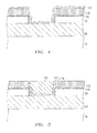
- FIGS. 1 and 2 show, in cross section, preliminary steps in the formation of trench isolation.
- FIGS. 3A and 3B show problems with prior art approaches.
- FIGS. 4 and 5 show steps in the inventive process.
- FIG. 1 A section of an SOI (silicon on insulator) wafer 10 is shown in FIG. 1 and following figures.
- This example is that of a silicon substrate 10 with a silicon device layer 30 , separated by an implanted SIMOX (Separation by IMplantation of OXygen) layer 20 , but bonded oxide insulating layers and Silicon-germanium device layers may also benefit from the invention.
- SIMOX Separatation by IMplantation of OXygen
- An aperture 50 has been etched through pad oxide 110 (illustratively 8 nm of thermal oxide) and pad nitride 120 (illustratively 120 nm of LPCVD Si 3 N 4 ) and silicon device layer 30 (illustratively 120 nm).
- the etch for the pad oxide and nitride is an NF 3 /Ar RIE (reactive ion etch) and the etch for device layer 30 is HBr and Cl 2 . This latter etch is very selective to oxide, so that, for the parameters specified, only about 10 nm of insulating layer (buried oxide, BOX) 20 is removed.
- FIG. 2 shows the result of a rapid thermal oxidation of the vertical walls of device layer 30 , producing 10-30 nm of oxide 112 at the thickest point. This provides sufficient corner rounding to prevent the occurrence of corner leakage during device operation.
- a problem with this technique is that the thickest portion of the oxide 112 is toward the center and top of the trench, leaving a recessed portion or negative trench angle 114 at the bottom near the corners.
- a fill with HDP oxide 130 leaves voids 115 at the bottom corners, since the fill tends to deposit directionally. In operation, these voids present the problem.
- planarization and wet chemical etching will recess the HDP oxide height or thickness.
- Eventual exposure of the void and expansion due to wet etching leaves a receptacle for polysilicon conductor material to deposit. Such an occurrence will electrically short neighboring devices, leading to product failure.
- a fill with LPCVD oxide 130 ′ (in FIG. 3B) fills in the bottom corners, but leaves a void or seam 115 ′ at the center.
- This center void has the same drawback previously discussed. It, too, can fill with polysilicon conductive material and cause failure due to device shorting. Failure due to a center void is likely to occur more readily than failure due to a bottom corner since the center void is in closer proximity to the device surface and therefore more easily exposed during processing.
- a preliminary low density oxide liner 152 is deposited, having a thickness in this example of between 25 nm to 45 nm.
- the actual thickness required is dependent upon the deposition technique used, the resulting liner density, and the degree of recess at the bottom corner of the starting trench.
- a thickness of about 15 nm greater than the thickness of liner 112 gives sufficient filling margin in the case of LPCVD.
- a thickness of about 30 nm greater than the thickness of liner 112 is preferred.
- preliminary liner deposition techniques include LPCVD TEOS (TetraEthyl OrthoSilicate) and RTCVD oxide.
- LPCVD TEOS TetraEthyl OrthoSilicate
- RTCVD oxide TetraEthyl OrthoSilicate
- liner 152 is deposited at a temperature in the range of 620-700 degrees C., with 620 degrees preferred, a chemistry of tetraethyl orthosilicate and pressure range of 200 to 1000 mTorr, with 1000 mTorr preferred.
- the deposition is preferably done at a temperature in the range of 700 to 775 degrees C., with 775 degrees C. preferred, a chemistry of N 2 O and SiH 4 and pressure range of 15 to 75 Torr, with 15 Torr preferred.
- the desired result is to apply an intermediate layer of only moderate conformality in a manner to reduce the thickness difference of the thermal oxide passivation layer: i.e. thicker where the passivation layer is thin and vice versa.
- the examples have been given as an illustration of possible approaches. Those skilled in the art will readily be able, in the light of this disclosure, to modify the processes illustrated to suit their conditions and to apply the teachings to other processes: e.g. PECVD.
- a HDP oxide layer 155 is deposited to a nominal thickness which is dependent upon on the technology node and the corresponding trench depth for that node.
- a densification step illustratively comprising a rapid thermal anneal at 1100 degrees C. in Argon/O 2 densifies preliminary liner 112 , so that the wet etching rate (in a conventional BHF or DHF mixture) is similar for HDP oxide 155 and the low density preliminary liner oxide (such as TEOS) 112 .
- the densification can be done at any convenient time.
- the trench fill (HDP and liner) is then planarized, using nitride 120 as a polish stop.
Abstract
Description
Claims (16)
Priority Applications (1)
| Application Number | Priority Date | Filing Date | Title |
|---|---|---|---|
| US10/214,510 US6825097B2 (en) | 2002-08-07 | 2002-08-07 | Triple oxide fill for trench isolation |
Applications Claiming Priority (1)
| Application Number | Priority Date | Filing Date | Title |
|---|---|---|---|
| US10/214,510 US6825097B2 (en) | 2002-08-07 | 2002-08-07 | Triple oxide fill for trench isolation |
Publications (2)
| Publication Number | Publication Date |
|---|---|
| US20040029352A1 US20040029352A1 (en) | 2004-02-12 |
| US6825097B2 true US6825097B2 (en) | 2004-11-30 |
Family
ID=31494664
Family Applications (1)
| Application Number | Title | Priority Date | Filing Date |
|---|---|---|---|
| US10/214,510 Expired - Lifetime US6825097B2 (en) | 2002-08-07 | 2002-08-07 | Triple oxide fill for trench isolation |
Country Status (1)
| Country | Link |
|---|---|
| US (1) | US6825097B2 (en) |
Cited By (3)
| Publication number | Priority date | Publication date | Assignee | Title |
|---|---|---|---|---|
| US20070232021A1 (en) * | 2005-12-07 | 2007-10-04 | Hynix Semiconductor Inc. | Method for Forming Isolation Layer in Semiconductor Device |
| US20080003739A1 (en) * | 2006-06-29 | 2008-01-03 | Hynix Semiconductor Inc. | Method for forming isolation structure of flash memory device |
| US8916950B2 (en) | 2011-10-18 | 2014-12-23 | International Business Machines Corporation | Shallow trench isolation structure having a nitride plug |
Families Citing this family (29)
| Publication number | Priority date | Publication date | Assignee | Title |
|---|---|---|---|---|
| US6800530B2 (en) * | 2003-01-14 | 2004-10-05 | International Business Machines Corporation | Triple layer hard mask for gate patterning to fabricate scaled CMOS transistors |
| KR100734670B1 (en) * | 2005-12-26 | 2007-07-02 | 동부일렉트로닉스 주식회사 | Method for fabricating semiconductor device |
| US8232176B2 (en) | 2006-06-22 | 2012-07-31 | Applied Materials, Inc. | Dielectric deposition and etch back processes for bottom up gapfill |
| US7867923B2 (en) | 2007-10-22 | 2011-01-11 | Applied Materials, Inc. | High quality silicon oxide films by remote plasma CVD from disilane precursors |
| US8357435B2 (en) * | 2008-05-09 | 2013-01-22 | Applied Materials, Inc. | Flowable dielectric equipment and processes |
| US20100081293A1 (en) * | 2008-10-01 | 2010-04-01 | Applied Materials, Inc. | Methods for forming silicon nitride based film or silicon carbon based film |
| US8511281B2 (en) * | 2009-07-10 | 2013-08-20 | Tula Technology, Inc. | Skip fire engine control |
| US8980382B2 (en) * | 2009-12-02 | 2015-03-17 | Applied Materials, Inc. | Oxygen-doping for non-carbon radical-component CVD films |
| US8741788B2 (en) * | 2009-08-06 | 2014-06-03 | Applied Materials, Inc. | Formation of silicon oxide using non-carbon flowable CVD processes |
| US8449942B2 (en) * | 2009-11-12 | 2013-05-28 | Applied Materials, Inc. | Methods of curing non-carbon flowable CVD films |
| SG181670A1 (en) * | 2009-12-30 | 2012-07-30 | Applied Materials Inc | Dielectric film growth with radicals produced using flexible nitrogen/hydrogen ratio |
| US20110159213A1 (en) * | 2009-12-30 | 2011-06-30 | Applied Materials, Inc. | Chemical vapor deposition improvements through radical-component modification |
| US8329262B2 (en) | 2010-01-05 | 2012-12-11 | Applied Materials, Inc. | Dielectric film formation using inert gas excitation |
| JP2013517616A (en) * | 2010-01-06 | 2013-05-16 | アプライド マテリアルズ インコーポレイテッド | Flowable dielectrics using oxide liners |
| SG182333A1 (en) | 2010-01-07 | 2012-08-30 | Applied Materials Inc | In-situ ozone cure for radical-component cvd |
| CN102844848A (en) * | 2010-03-05 | 2012-12-26 | 应用材料公司 | Conformal layers by radical-component cvd |
| US9285168B2 (en) | 2010-10-05 | 2016-03-15 | Applied Materials, Inc. | Module for ozone cure and post-cure moisture treatment |
| US8664127B2 (en) | 2010-10-15 | 2014-03-04 | Applied Materials, Inc. | Two silicon-containing precursors for gapfill enhancing dielectric liner |
| US10283321B2 (en) | 2011-01-18 | 2019-05-07 | Applied Materials, Inc. | Semiconductor processing system and methods using capacitively coupled plasma |
| US8450191B2 (en) | 2011-01-24 | 2013-05-28 | Applied Materials, Inc. | Polysilicon films by HDP-CVD |
| US8716154B2 (en) | 2011-03-04 | 2014-05-06 | Applied Materials, Inc. | Reduced pattern loading using silicon oxide multi-layers |
| US8445078B2 (en) | 2011-04-20 | 2013-05-21 | Applied Materials, Inc. | Low temperature silicon oxide conversion |
| US8466073B2 (en) | 2011-06-03 | 2013-06-18 | Applied Materials, Inc. | Capping layer for reduced outgassing |
| US9404178B2 (en) | 2011-07-15 | 2016-08-02 | Applied Materials, Inc. | Surface treatment and deposition for reduced outgassing |
| US8617989B2 (en) | 2011-09-26 | 2013-12-31 | Applied Materials, Inc. | Liner property improvement |
| US8551891B2 (en) | 2011-10-04 | 2013-10-08 | Applied Materials, Inc. | Remote plasma burn-in |
| US8889566B2 (en) | 2012-09-11 | 2014-11-18 | Applied Materials, Inc. | Low cost flowable dielectric films |
| US9018108B2 (en) | 2013-01-25 | 2015-04-28 | Applied Materials, Inc. | Low shrinkage dielectric films |
| US9412581B2 (en) | 2014-07-16 | 2016-08-09 | Applied Materials, Inc. | Low-K dielectric gapfill by flowable deposition |
Citations (18)
| Publication number | Priority date | Publication date | Assignee | Title |
|---|---|---|---|---|
| US4656497A (en) | 1984-11-01 | 1987-04-07 | Ncr Corporation | Trench isolation structures |
| US5099304A (en) | 1988-12-08 | 1992-03-24 | Nec Corporation | Semiconductor device with insulating isolation groove |
| US5719085A (en) | 1995-09-29 | 1998-02-17 | Intel Corporation | Shallow trench isolation technique |
| US6033970A (en) | 1997-11-06 | 2000-03-07 | Lg Semicon Co., Ltd. | Method for forming device-isolating layer in semiconductor device |
| US6037018A (en) | 1998-07-01 | 2000-03-14 | Taiwan Semiconductor Maufacturing Company | Shallow trench isolation filled by high density plasma chemical vapor deposition |
| US6118168A (en) | 1995-09-29 | 2000-09-12 | Intel Corporation | Trench isolation process using nitrogen preconditioning to reduce crystal defects |
| WO2000060659A1 (en) | 1999-04-02 | 2000-10-12 | Silicon Valley Group, Thermal Systems Llc | Improved trench isolation process to deposit a trench fill oxide prior to sidewall liner oxidation growth |
| US6140208A (en) | 1999-02-05 | 2000-10-31 | International Business Machines Corporation | Shallow trench isolation (STI) with bilayer of oxide-nitride for VLSI applications |
| US6180467B1 (en) | 1998-12-15 | 2001-01-30 | United Microelectronics Corp. | Method of fabricating shallow trench isolation |
| US6194283B1 (en) | 1997-10-29 | 2001-02-27 | Advanced Micro Devices, Inc. | High density trench fill due to new spacer fill method including isotropically etching silicon nitride spacers |
| US6214698B1 (en) | 2000-01-11 | 2001-04-10 | Taiwan Semiconductor Manufacturing Company | Shallow trench isolation methods employing gap filling doped silicon oxide dielectric layer |
| US6255194B1 (en) | 1999-06-03 | 2001-07-03 | Samsung Electronics Co., Ltd. | Trench isolation method |
| US6258676B1 (en) | 1999-11-01 | 2001-07-10 | Chartered Semiconductor Manufacturing Ltd. | Method for forming a shallow trench isolation using HDP silicon oxynitride |
| US6261908B1 (en) | 1998-07-27 | 2001-07-17 | Advanced Micro Devices, Inc. | Buried local interconnect |
| US6271153B1 (en) | 1998-07-22 | 2001-08-07 | Micron Technology, Inc. | Semiconductor processing method and trench isolation method |
| US6271143B1 (en) | 1999-05-06 | 2001-08-07 | Motorola, Inc. | Method for preventing trench fill erosion |
| US6472301B1 (en) * | 1999-10-19 | 2002-10-29 | Infineon Technologies Ag | Method and structure for shallow trench isolation |
| US6521510B1 (en) * | 2001-03-23 | 2003-02-18 | Advanced Micro Devices, Inc. | Method for shallow trench isolation with removal of strained island edges |
-
2002
- 2002-08-07 US US10/214,510 patent/US6825097B2/en not_active Expired - Lifetime
Patent Citations (18)
| Publication number | Priority date | Publication date | Assignee | Title |
|---|---|---|---|---|
| US4656497A (en) | 1984-11-01 | 1987-04-07 | Ncr Corporation | Trench isolation structures |
| US5099304A (en) | 1988-12-08 | 1992-03-24 | Nec Corporation | Semiconductor device with insulating isolation groove |
| US5719085A (en) | 1995-09-29 | 1998-02-17 | Intel Corporation | Shallow trench isolation technique |
| US6118168A (en) | 1995-09-29 | 2000-09-12 | Intel Corporation | Trench isolation process using nitrogen preconditioning to reduce crystal defects |
| US6194283B1 (en) | 1997-10-29 | 2001-02-27 | Advanced Micro Devices, Inc. | High density trench fill due to new spacer fill method including isotropically etching silicon nitride spacers |
| US6033970A (en) | 1997-11-06 | 2000-03-07 | Lg Semicon Co., Ltd. | Method for forming device-isolating layer in semiconductor device |
| US6037018A (en) | 1998-07-01 | 2000-03-14 | Taiwan Semiconductor Maufacturing Company | Shallow trench isolation filled by high density plasma chemical vapor deposition |
| US6271153B1 (en) | 1998-07-22 | 2001-08-07 | Micron Technology, Inc. | Semiconductor processing method and trench isolation method |
| US6261908B1 (en) | 1998-07-27 | 2001-07-17 | Advanced Micro Devices, Inc. | Buried local interconnect |
| US6180467B1 (en) | 1998-12-15 | 2001-01-30 | United Microelectronics Corp. | Method of fabricating shallow trench isolation |
| US6140208A (en) | 1999-02-05 | 2000-10-31 | International Business Machines Corporation | Shallow trench isolation (STI) with bilayer of oxide-nitride for VLSI applications |
| WO2000060659A1 (en) | 1999-04-02 | 2000-10-12 | Silicon Valley Group, Thermal Systems Llc | Improved trench isolation process to deposit a trench fill oxide prior to sidewall liner oxidation growth |
| US6271143B1 (en) | 1999-05-06 | 2001-08-07 | Motorola, Inc. | Method for preventing trench fill erosion |
| US6255194B1 (en) | 1999-06-03 | 2001-07-03 | Samsung Electronics Co., Ltd. | Trench isolation method |
| US6472301B1 (en) * | 1999-10-19 | 2002-10-29 | Infineon Technologies Ag | Method and structure for shallow trench isolation |
| US6258676B1 (en) | 1999-11-01 | 2001-07-10 | Chartered Semiconductor Manufacturing Ltd. | Method for forming a shallow trench isolation using HDP silicon oxynitride |
| US6214698B1 (en) | 2000-01-11 | 2001-04-10 | Taiwan Semiconductor Manufacturing Company | Shallow trench isolation methods employing gap filling doped silicon oxide dielectric layer |
| US6521510B1 (en) * | 2001-03-23 | 2003-02-18 | Advanced Micro Devices, Inc. | Method for shallow trench isolation with removal of strained island edges |
Cited By (5)
| Publication number | Priority date | Publication date | Assignee | Title |
|---|---|---|---|---|
| US20070232021A1 (en) * | 2005-12-07 | 2007-10-04 | Hynix Semiconductor Inc. | Method for Forming Isolation Layer in Semiconductor Device |
| US20080003739A1 (en) * | 2006-06-29 | 2008-01-03 | Hynix Semiconductor Inc. | Method for forming isolation structure of flash memory device |
| US7713887B2 (en) * | 2006-12-07 | 2010-05-11 | Hynix Semiconductor Inc. | Method for forming isolation layer in semiconductor device |
| US8916950B2 (en) | 2011-10-18 | 2014-12-23 | International Business Machines Corporation | Shallow trench isolation structure having a nitride plug |
| US9443929B2 (en) | 2011-10-18 | 2016-09-13 | International Business Machines Corporation | Shallow trench isolation structure having a nitride plug |
Also Published As
| Publication number | Publication date |
|---|---|
| US20040029352A1 (en) | 2004-02-12 |
Similar Documents
| Publication | Publication Date | Title |
|---|---|---|
| US6825097B2 (en) | Triple oxide fill for trench isolation | |
| US9799727B2 (en) | Isolation trench fill using oxide liner and nitride etch back technique with dual trench depth capability | |
| US5811315A (en) | Method of forming and planarizing deep isolation trenches in a silicon-on-insulator (SOI) structure | |
| US5933748A (en) | Shallow trench isolation process | |
| US7038289B2 (en) | Deep insulating trench | |
| US6372605B1 (en) | Additional etching to decrease polishing time for shallow-trench isolation in semiconductor processing | |
| US6727159B2 (en) | Method of forming a shallow trench isolation in a semiconductor substrate | |
| US6627514B1 (en) | Semiconductor device having a Y-shaped isolation layer and simplified method for manufacturing the Y-shaped isolation layer to prevent divot formation | |
| US20040099906A1 (en) | Trench isolation without grooving | |
| US5918131A (en) | Method of manufacturing a shallow trench isolation structure | |
| US6599813B2 (en) | Method of forming shallow trench isolation for thin silicon-on-insulator substrates | |
| US6410403B1 (en) | Method for planarizing a shallow trench isolation | |
| US6649488B2 (en) | Method of shallow trench isolation | |
| US6818526B2 (en) | Method for moat nitride pull back for shallow trench isolation | |
| US20040058507A1 (en) | Manufacturing method for a shallow trench isolation region with high aspect ratio | |
| US6358785B1 (en) | Method for forming shallow trench isolation structures | |
| US6960530B2 (en) | Method of reducing the aspect ratio of a trench | |
| EP0954022B1 (en) | Method for providing shallow trench isolation of transistors | |
| US20060270185A1 (en) | Method of forming isolation film of semiconductor device | |
| US6242322B1 (en) | Method for forming shallow trench isolation filled with high-density plasma oxide layer | |
| US7154159B2 (en) | Trench isolation structure and method of forming the same | |
| US6849493B2 (en) | Methods of forming polished material and methods of forming isolation regions | |
| US20050009294A1 (en) | Process for the formation of dielectric isolation structures in semiconductor devices | |
| US6403492B1 (en) | Method of manufacturing semiconductor devices with trench isolation | |
| KR100508535B1 (en) | Method for forming gate pole in a semiconductor |
Legal Events
| Date | Code | Title | Description |
|---|---|---|---|
| AS | Assignment |
Owner name: INTERNATIONAL BUSINESS MACHINES CORPORATION, NEW Y Free format text: ASSIGNMENT OF ASSIGNORS INTEREST;ASSIGNORS:BEYER, KLAUS D.;O'NEIL, PATRICIA A.;RYAN, DEBORAH A.;AND OTHERS;REEL/FRAME:013190/0793;SIGNING DATES FROM 20020718 TO 20020806 |
|
| FEPP | Fee payment procedure |
Free format text: PAYOR NUMBER ASSIGNED (ORIGINAL EVENT CODE: ASPN); ENTITY STATUS OF PATENT OWNER: LARGE ENTITY |
|
| STCF | Information on status: patent grant |
Free format text: PATENTED CASE |
|
| FPAY | Fee payment |
Year of fee payment: 4 |
|
| REMI | Maintenance fee reminder mailed | ||
| FPAY | Fee payment |
Year of fee payment: 8 |
|
| SULP | Surcharge for late payment |
Year of fee payment: 7 |
|
| AS | Assignment |
Owner name: GLOBALFOUNDRIES U.S. 2 LLC, NEW YORK Free format text: ASSIGNMENT OF ASSIGNORS INTEREST;ASSIGNOR:INTERNATIONAL BUSINESS MACHINES CORPORATION;REEL/FRAME:036550/0001 Effective date: 20150629 |
|
| AS | Assignment |
Owner name: GLOBALFOUNDRIES INC., CAYMAN ISLANDS Free format text: ASSIGNMENT OF ASSIGNORS INTEREST;ASSIGNORS:GLOBALFOUNDRIES U.S. 2 LLC;GLOBALFOUNDRIES U.S. INC.;REEL/FRAME:036779/0001 Effective date: 20150910 |
|
| FPAY | Fee payment |
Year of fee payment: 12 |
|
| AS | Assignment |
Owner name: WILMINGTON TRUST, NATIONAL ASSOCIATION, DELAWARE Free format text: SECURITY AGREEMENT;ASSIGNOR:GLOBALFOUNDRIES INC.;REEL/FRAME:049490/0001 Effective date: 20181127 |
|
| AS | Assignment |
Owner name: GLOBALFOUNDRIES U.S. INC., CALIFORNIA Free format text: ASSIGNMENT OF ASSIGNORS INTEREST;ASSIGNOR:GLOBALFOUNDRIES INC.;REEL/FRAME:054633/0001 Effective date: 20201022 |
|
| AS | Assignment |
Owner name: GLOBALFOUNDRIES INC., CAYMAN ISLANDS Free format text: RELEASE BY SECURED PARTY;ASSIGNOR:WILMINGTON TRUST, NATIONAL ASSOCIATION;REEL/FRAME:054636/0001 Effective date: 20201117 |
|
| AS | Assignment |
Owner name: GLOBALFOUNDRIES U.S. INC., NEW YORK Free format text: RELEASE BY SECURED PARTY;ASSIGNOR:WILMINGTON TRUST, NATIONAL ASSOCIATION;REEL/FRAME:056987/0001 Effective date: 20201117 |