US6806428B1 - Module component and method of manufacturing the same - Google Patents
Module component and method of manufacturing the same Download PDFInfo
- Publication number
- US6806428B1 US6806428B1 US09/719,631 US71963101A US6806428B1 US 6806428 B1 US6806428 B1 US 6806428B1 US 71963101 A US71963101 A US 71963101A US 6806428 B1 US6806428 B1 US 6806428B1
- Authority
- US
- United States
- Prior art keywords
- substrate
- penetration holes
- chip
- component
- disposed
- Prior art date
- Legal status (The legal status is an assumption and is not a legal conclusion. Google has not performed a legal analysis and makes no representation as to the accuracy of the status listed.)
- Expired - Lifetime
Links
Images


Classifications
-
- H—ELECTRICITY
- H05—ELECTRIC TECHNIQUES NOT OTHERWISE PROVIDED FOR
- H05K—PRINTED CIRCUITS; CASINGS OR CONSTRUCTIONAL DETAILS OF ELECTRIC APPARATUS; MANUFACTURE OF ASSEMBLAGES OF ELECTRICAL COMPONENTS
- H05K1/00—Printed circuits
- H05K1/18—Printed circuits structurally associated with non-printed electric components
- H05K1/182—Printed circuits structurally associated with non-printed electric components associated with components mounted in the printed circuit board, e.g. insert mounted components [IMC]
- H05K1/184—Components including terminals inserted in holes through the printed circuit board and connected to printed contacts on the walls of the holes or at the edges thereof or protruding over or into the holes
-
- H—ELECTRICITY
- H01—ELECTRIC ELEMENTS
- H01L—SEMICONDUCTOR DEVICES NOT COVERED BY CLASS H10
- H01L23/00—Details of semiconductor or other solid state devices
- H01L23/52—Arrangements for conducting electric current within the device in operation from one component to another, i.e. interconnections, e.g. wires, lead frames
- H01L23/538—Arrangements for conducting electric current within the device in operation from one component to another, i.e. interconnections, e.g. wires, lead frames the interconnection structure between a plurality of semiconductor chips being formed on, or in, insulating substrates
- H01L23/5383—Multilayer substrates
-
- H—ELECTRICITY
- H01—ELECTRIC ELEMENTS
- H01L—SEMICONDUCTOR DEVICES NOT COVERED BY CLASS H10
- H01L23/00—Details of semiconductor or other solid state devices
- H01L23/52—Arrangements for conducting electric current within the device in operation from one component to another, i.e. interconnections, e.g. wires, lead frames
- H01L23/538—Arrangements for conducting electric current within the device in operation from one component to another, i.e. interconnections, e.g. wires, lead frames the interconnection structure between a plurality of semiconductor chips being formed on, or in, insulating substrates
- H01L23/5386—Geometry or layout of the interconnection structure
-
- H—ELECTRICITY
- H01—ELECTRIC ELEMENTS
- H01L—SEMICONDUCTOR DEVICES NOT COVERED BY CLASS H10
- H01L25/00—Assemblies consisting of a plurality of individual semiconductor or other solid state devices ; Multistep manufacturing processes thereof
- H01L25/16—Assemblies consisting of a plurality of individual semiconductor or other solid state devices ; Multistep manufacturing processes thereof the devices being of types provided for in two or more different main groups of groups H01L27/00 - H01L33/00, or in a single subclass of H10K, H10N, e.g. forming hybrid circuits
-
- H—ELECTRICITY
- H05—ELECTRIC TECHNIQUES NOT OTHERWISE PROVIDED FOR
- H05K—PRINTED CIRCUITS; CASINGS OR CONSTRUCTIONAL DETAILS OF ELECTRIC APPARATUS; MANUFACTURE OF ASSEMBLAGES OF ELECTRICAL COMPONENTS
- H05K1/00—Printed circuits
- H05K1/02—Details
- H05K1/0213—Electrical arrangements not otherwise provided for
- H05K1/0216—Reduction of cross-talk, noise or electromagnetic interference
- H05K1/023—Reduction of cross-talk, noise or electromagnetic interference using auxiliary mounted passive components or auxiliary substances
-
- H—ELECTRICITY
- H05—ELECTRIC TECHNIQUES NOT OTHERWISE PROVIDED FOR
- H05K—PRINTED CIRCUITS; CASINGS OR CONSTRUCTIONAL DETAILS OF ELECTRIC APPARATUS; MANUFACTURE OF ASSEMBLAGES OF ELECTRICAL COMPONENTS
- H05K1/00—Printed circuits
- H05K1/18—Printed circuits structurally associated with non-printed electric components
- H05K1/182—Printed circuits structurally associated with non-printed electric components associated with components mounted in the printed circuit board, e.g. insert mounted components [IMC]
- H05K1/185—Components encapsulated in the insulating substrate of the printed circuit or incorporated in internal layers of a multilayer circuit
-
- H—ELECTRICITY
- H01—ELECTRIC ELEMENTS
- H01L—SEMICONDUCTOR DEVICES NOT COVERED BY CLASS H10
- H01L2224/00—Indexing scheme for arrangements for connecting or disconnecting semiconductor or solid-state bodies and methods related thereto as covered by H01L24/00
- H01L2224/01—Means for bonding being attached to, or being formed on, the surface to be connected, e.g. chip-to-package, die-attach, "first-level" interconnects; Manufacturing methods related thereto
- H01L2224/10—Bump connectors; Manufacturing methods related thereto
- H01L2224/15—Structure, shape, material or disposition of the bump connectors after the connecting process
- H01L2224/16—Structure, shape, material or disposition of the bump connectors after the connecting process of an individual bump connector
- H01L2224/161—Disposition
- H01L2224/16151—Disposition the bump connector connecting between a semiconductor or solid-state body and an item not being a semiconductor or solid-state body, e.g. chip-to-substrate, chip-to-passive
- H01L2224/16221—Disposition the bump connector connecting between a semiconductor or solid-state body and an item not being a semiconductor or solid-state body, e.g. chip-to-substrate, chip-to-passive the body and the item being stacked
- H01L2224/16225—Disposition the bump connector connecting between a semiconductor or solid-state body and an item not being a semiconductor or solid-state body, e.g. chip-to-substrate, chip-to-passive the body and the item being stacked the item being non-metallic, e.g. insulating substrate with or without metallisation
- H01L2224/16235—Disposition the bump connector connecting between a semiconductor or solid-state body and an item not being a semiconductor or solid-state body, e.g. chip-to-substrate, chip-to-passive the body and the item being stacked the item being non-metallic, e.g. insulating substrate with or without metallisation the bump connector connecting to a via metallisation of the item
-
- H—ELECTRICITY
- H01—ELECTRIC ELEMENTS
- H01L—SEMICONDUCTOR DEVICES NOT COVERED BY CLASS H10
- H01L2224/00—Indexing scheme for arrangements for connecting or disconnecting semiconductor or solid-state bodies and methods related thereto as covered by H01L24/00
- H01L2224/01—Means for bonding being attached to, or being formed on, the surface to be connected, e.g. chip-to-package, die-attach, "first-level" interconnects; Manufacturing methods related thereto
- H01L2224/10—Bump connectors; Manufacturing methods related thereto
- H01L2224/15—Structure, shape, material or disposition of the bump connectors after the connecting process
- H01L2224/16—Structure, shape, material or disposition of the bump connectors after the connecting process of an individual bump connector
- H01L2224/161—Disposition
- H01L2224/16151—Disposition the bump connector connecting between a semiconductor or solid-state body and an item not being a semiconductor or solid-state body, e.g. chip-to-substrate, chip-to-passive
- H01L2224/16221—Disposition the bump connector connecting between a semiconductor or solid-state body and an item not being a semiconductor or solid-state body, e.g. chip-to-substrate, chip-to-passive the body and the item being stacked
- H01L2224/16265—Disposition the bump connector connecting between a semiconductor or solid-state body and an item not being a semiconductor or solid-state body, e.g. chip-to-substrate, chip-to-passive the body and the item being stacked the item being a discrete passive component
-
- H—ELECTRICITY
- H01—ELECTRIC ELEMENTS
- H01L—SEMICONDUCTOR DEVICES NOT COVERED BY CLASS H10
- H01L2224/00—Indexing scheme for arrangements for connecting or disconnecting semiconductor or solid-state bodies and methods related thereto as covered by H01L24/00
- H01L2224/73—Means for bonding being of different types provided for in two or more of groups H01L2224/10, H01L2224/18, H01L2224/26, H01L2224/34, H01L2224/42, H01L2224/50, H01L2224/63, H01L2224/71
- H01L2224/732—Location after the connecting process
- H01L2224/73201—Location after the connecting process on the same surface
- H01L2224/73203—Bump and layer connectors
- H01L2224/73204—Bump and layer connectors the bump connector being embedded into the layer connector
-
- H—ELECTRICITY
- H01—ELECTRIC ELEMENTS
- H01L—SEMICONDUCTOR DEVICES NOT COVERED BY CLASS H10
- H01L2924/00—Indexing scheme for arrangements or methods for connecting or disconnecting semiconductor or solid-state bodies as covered by H01L24/00
- H01L2924/01—Chemical elements
- H01L2924/01078—Platinum [Pt]
-
- H—ELECTRICITY
- H01—ELECTRIC ELEMENTS
- H01L—SEMICONDUCTOR DEVICES NOT COVERED BY CLASS H10
- H01L2924/00—Indexing scheme for arrangements or methods for connecting or disconnecting semiconductor or solid-state bodies as covered by H01L24/00
- H01L2924/19—Details of hybrid assemblies other than the semiconductor or other solid state devices to be connected
- H01L2924/191—Disposition
- H01L2924/19101—Disposition of discrete passive components
- H01L2924/19102—Disposition of discrete passive components in a stacked assembly with the semiconductor or solid state device
- H01L2924/19103—Disposition of discrete passive components in a stacked assembly with the semiconductor or solid state device interposed between the semiconductor or solid-state device and the die mounting substrate, i.e. chip-on-passive
-
- H—ELECTRICITY
- H01—ELECTRIC ELEMENTS
- H01L—SEMICONDUCTOR DEVICES NOT COVERED BY CLASS H10
- H01L2924/00—Indexing scheme for arrangements or methods for connecting or disconnecting semiconductor or solid-state bodies as covered by H01L24/00
- H01L2924/19—Details of hybrid assemblies other than the semiconductor or other solid state devices to be connected
- H01L2924/191—Disposition
- H01L2924/19101—Disposition of discrete passive components
- H01L2924/19105—Disposition of discrete passive components in a side-by-side arrangement on a common die mounting substrate
-
- H—ELECTRICITY
- H05—ELECTRIC TECHNIQUES NOT OTHERWISE PROVIDED FOR
- H05K—PRINTED CIRCUITS; CASINGS OR CONSTRUCTIONAL DETAILS OF ELECTRIC APPARATUS; MANUFACTURE OF ASSEMBLAGES OF ELECTRICAL COMPONENTS
- H05K1/00—Printed circuits
- H05K1/02—Details
- H05K1/0213—Electrical arrangements not otherwise provided for
- H05K1/0216—Reduction of cross-talk, noise or electromagnetic interference
- H05K1/023—Reduction of cross-talk, noise or electromagnetic interference using auxiliary mounted passive components or auxiliary substances
- H05K1/0231—Capacitors or dielectric substances
-
- H—ELECTRICITY
- H05—ELECTRIC TECHNIQUES NOT OTHERWISE PROVIDED FOR
- H05K—PRINTED CIRCUITS; CASINGS OR CONSTRUCTIONAL DETAILS OF ELECTRIC APPARATUS; MANUFACTURE OF ASSEMBLAGES OF ELECTRICAL COMPONENTS
- H05K2201/00—Indexing scheme relating to printed circuits covered by H05K1/00
- H05K2201/09—Shape and layout
- H05K2201/09009—Substrate related
- H05K2201/09118—Moulded substrate
-
- H—ELECTRICITY
- H05—ELECTRIC TECHNIQUES NOT OTHERWISE PROVIDED FOR
- H05K—PRINTED CIRCUITS; CASINGS OR CONSTRUCTIONAL DETAILS OF ELECTRIC APPARATUS; MANUFACTURE OF ASSEMBLAGES OF ELECTRICAL COMPONENTS
- H05K2201/00—Indexing scheme relating to printed circuits covered by H05K1/00
- H05K2201/09—Shape and layout
- H05K2201/09818—Shape or layout details not covered by a single group of H05K2201/09009 - H05K2201/09809
- H05K2201/09827—Tapered, e.g. tapered hole, via or groove
-
- H—ELECTRICITY
- H05—ELECTRIC TECHNIQUES NOT OTHERWISE PROVIDED FOR
- H05K—PRINTED CIRCUITS; CASINGS OR CONSTRUCTIONAL DETAILS OF ELECTRIC APPARATUS; MANUFACTURE OF ASSEMBLAGES OF ELECTRICAL COMPONENTS
- H05K2201/00—Indexing scheme relating to printed circuits covered by H05K1/00
- H05K2201/10—Details of components or other objects attached to or integrated in a printed circuit board
- H05K2201/10007—Types of components
- H05K2201/10204—Dummy component, dummy PCB or template, e.g. for monitoring, controlling of processes, comparing, scanning
-
- H—ELECTRICITY
- H05—ELECTRIC TECHNIQUES NOT OTHERWISE PROVIDED FOR
- H05K—PRINTED CIRCUITS; CASINGS OR CONSTRUCTIONAL DETAILS OF ELECTRIC APPARATUS; MANUFACTURE OF ASSEMBLAGES OF ELECTRICAL COMPONENTS
- H05K2201/00—Indexing scheme relating to printed circuits covered by H05K1/00
- H05K2201/10—Details of components or other objects attached to or integrated in a printed circuit board
- H05K2201/10431—Details of mounted components
- H05K2201/10507—Involving several components
- H05K2201/1053—Mounted components directly electrically connected to each other, i.e. not via the PCB
-
- H—ELECTRICITY
- H05—ELECTRIC TECHNIQUES NOT OTHERWISE PROVIDED FOR
- H05K—PRINTED CIRCUITS; CASINGS OR CONSTRUCTIONAL DETAILS OF ELECTRIC APPARATUS; MANUFACTURE OF ASSEMBLAGES OF ELECTRICAL COMPONENTS
- H05K2201/00—Indexing scheme relating to printed circuits covered by H05K1/00
- H05K2201/10—Details of components or other objects attached to or integrated in a printed circuit board
- H05K2201/10613—Details of electrical connections of non-printed components, e.g. special leads
- H05K2201/10621—Components characterised by their electrical contacts
- H05K2201/10636—Leadless chip, e.g. chip capacitor or resistor
-
- H—ELECTRICITY
- H05—ELECTRIC TECHNIQUES NOT OTHERWISE PROVIDED FOR
- H05K—PRINTED CIRCUITS; CASINGS OR CONSTRUCTIONAL DETAILS OF ELECTRIC APPARATUS; MANUFACTURE OF ASSEMBLAGES OF ELECTRICAL COMPONENTS
- H05K2203/00—Indexing scheme relating to apparatus or processes for manufacturing printed circuits covered by H05K3/00
- H05K2203/14—Related to the order of processing steps
- H05K2203/1461—Applying or finishing the circuit pattern after another process, e.g. after filling of vias with conductive paste, after making printed resistors
- H05K2203/1469—Circuit made after mounting or encapsulation of the components
-
- H—ELECTRICITY
- H05—ELECTRIC TECHNIQUES NOT OTHERWISE PROVIDED FOR
- H05K—PRINTED CIRCUITS; CASINGS OR CONSTRUCTIONAL DETAILS OF ELECTRIC APPARATUS; MANUFACTURE OF ASSEMBLAGES OF ELECTRICAL COMPONENTS
- H05K2203/00—Indexing scheme relating to apparatus or processes for manufacturing printed circuits covered by H05K3/00
- H05K2203/16—Inspection; Monitoring; Aligning
- H05K2203/161—Using chemical substances, e.g. colored or fluorescent, for facilitating optical or visual inspection
-
- H—ELECTRICITY
- H05—ELECTRIC TECHNIQUES NOT OTHERWISE PROVIDED FOR
- H05K—PRINTED CIRCUITS; CASINGS OR CONSTRUCTIONAL DETAILS OF ELECTRIC APPARATUS; MANUFACTURE OF ASSEMBLAGES OF ELECTRICAL COMPONENTS
- H05K3/00—Apparatus or processes for manufacturing printed circuits
- H05K3/40—Forming printed elements for providing electric connections to or between printed circuits
- H05K3/4038—Through-connections; Vertical interconnect access [VIA] connections
- H05K3/4046—Through-connections; Vertical interconnect access [VIA] connections using auxiliary conductive elements, e.g. metallic spheres, eyelets, pieces of wire
-
- H—ELECTRICITY
- H05—ELECTRIC TECHNIQUES NOT OTHERWISE PROVIDED FOR
- H05K—PRINTED CIRCUITS; CASINGS OR CONSTRUCTIONAL DETAILS OF ELECTRIC APPARATUS; MANUFACTURE OF ASSEMBLAGES OF ELECTRICAL COMPONENTS
- H05K3/00—Apparatus or processes for manufacturing printed circuits
- H05K3/46—Manufacturing multilayer circuits
- H05K3/4602—Manufacturing multilayer circuits characterized by a special circuit board as base or central core whereon additional circuit layers are built or additional circuit boards are laminated
-
- Y—GENERAL TAGGING OF NEW TECHNOLOGICAL DEVELOPMENTS; GENERAL TAGGING OF CROSS-SECTIONAL TECHNOLOGIES SPANNING OVER SEVERAL SECTIONS OF THE IPC; TECHNICAL SUBJECTS COVERED BY FORMER USPC CROSS-REFERENCE ART COLLECTIONS [XRACs] AND DIGESTS
- Y02—TECHNOLOGIES OR APPLICATIONS FOR MITIGATION OR ADAPTATION AGAINST CLIMATE CHANGE
- Y02P—CLIMATE CHANGE MITIGATION TECHNOLOGIES IN THE PRODUCTION OR PROCESSING OF GOODS
- Y02P70/00—Climate change mitigation technologies in the production process for final industrial or consumer products
- Y02P70/50—Manufacturing or production processes characterised by the final manufactured product
-
- Y—GENERAL TAGGING OF NEW TECHNOLOGICAL DEVELOPMENTS; GENERAL TAGGING OF CROSS-SECTIONAL TECHNOLOGIES SPANNING OVER SEVERAL SECTIONS OF THE IPC; TECHNICAL SUBJECTS COVERED BY FORMER USPC CROSS-REFERENCE ART COLLECTIONS [XRACs] AND DIGESTS
- Y10—TECHNICAL SUBJECTS COVERED BY FORMER USPC
- Y10T—TECHNICAL SUBJECTS COVERED BY FORMER US CLASSIFICATION
- Y10T29/00—Metal working
- Y10T29/49—Method of mechanical manufacture
- Y10T29/49002—Electrical device making
- Y10T29/49117—Conductor or circuit manufacturing
- Y10T29/49124—On flat or curved insulated base, e.g., printed circuit, etc.
- Y10T29/49126—Assembling bases
-
- Y—GENERAL TAGGING OF NEW TECHNOLOGICAL DEVELOPMENTS; GENERAL TAGGING OF CROSS-SECTIONAL TECHNOLOGIES SPANNING OVER SEVERAL SECTIONS OF THE IPC; TECHNICAL SUBJECTS COVERED BY FORMER USPC CROSS-REFERENCE ART COLLECTIONS [XRACs] AND DIGESTS
- Y10—TECHNICAL SUBJECTS COVERED BY FORMER USPC
- Y10T—TECHNICAL SUBJECTS COVERED BY FORMER US CLASSIFICATION
- Y10T29/00—Metal working
- Y10T29/49—Method of mechanical manufacture
- Y10T29/49002—Electrical device making
- Y10T29/49117—Conductor or circuit manufacturing
- Y10T29/49124—On flat or curved insulated base, e.g., printed circuit, etc.
- Y10T29/4913—Assembling to base an electrical component, e.g., capacitor, etc.
- Y10T29/49146—Assembling to base an electrical component, e.g., capacitor, etc. with encapsulating, e.g., potting, etc.
-
- Y—GENERAL TAGGING OF NEW TECHNOLOGICAL DEVELOPMENTS; GENERAL TAGGING OF CROSS-SECTIONAL TECHNOLOGIES SPANNING OVER SEVERAL SECTIONS OF THE IPC; TECHNICAL SUBJECTS COVERED BY FORMER USPC CROSS-REFERENCE ART COLLECTIONS [XRACs] AND DIGESTS
- Y10—TECHNICAL SUBJECTS COVERED BY FORMER USPC
- Y10T—TECHNICAL SUBJECTS COVERED BY FORMER US CLASSIFICATION
- Y10T29/00—Metal working
- Y10T29/49—Method of mechanical manufacture
- Y10T29/49002—Electrical device making
- Y10T29/49117—Conductor or circuit manufacturing
- Y10T29/49124—On flat or curved insulated base, e.g., printed circuit, etc.
- Y10T29/49155—Manufacturing circuit on or in base
- Y10T29/49158—Manufacturing circuit on or in base with molding of insulated base
-
- Y—GENERAL TAGGING OF NEW TECHNOLOGICAL DEVELOPMENTS; GENERAL TAGGING OF CROSS-SECTIONAL TECHNOLOGIES SPANNING OVER SEVERAL SECTIONS OF THE IPC; TECHNICAL SUBJECTS COVERED BY FORMER USPC CROSS-REFERENCE ART COLLECTIONS [XRACs] AND DIGESTS
- Y10—TECHNICAL SUBJECTS COVERED BY FORMER USPC
- Y10T—TECHNICAL SUBJECTS COVERED BY FORMER US CLASSIFICATION
- Y10T29/00—Metal working
- Y10T29/49—Method of mechanical manufacture
- Y10T29/49002—Electrical device making
- Y10T29/49117—Conductor or circuit manufacturing
- Y10T29/49169—Assembling electrical component directly to terminal or elongated conductor
- Y10T29/49171—Assembling electrical component directly to terminal or elongated conductor with encapsulating
- Y10T29/49172—Assembling electrical component directly to terminal or elongated conductor with encapsulating by molding of insulating material
Definitions
- the present invention relates to a module component composed by mounting a chip component in a circuit board or by molding a chip component, and a method of manufacturing the same.
- Japanese Laid-open Patent No. 63-169798 is known, and the structure as shown in FIG. 12 ( a ) realizes an equivalent circuit as shown in FIG. 12 ( b ).
- reference numeral 102 denotes a multi-layer substrate laminating ceramic substrates 121 through 126 in multiple layers.
- Capacitors 103 , 104 and resistor 105 are inserted in penetration holes 107 formed in multi-layer substrate 102 , and they are electrically connected by conductors 106 .
- capacitors 103 , 104 and resistor 105 must be finally baked together with multi-layer substrate 102 , and special components excellent in heat resistance are needed. But it is hard to obtain sufficient heat resisting effect as the size of the electronic components becomes smaller. Specified values may not be obtained due to characteristic deterioration or characteristic fluctuation by heat treatment at high temperature, and therefore, desired circuit characteristics and functions are not obtainable. The dimensions vary due to shrinkage and contraction by heat treatment at high temperature, and it is accordingly hard to obtain components of precise dimensions, and size reduction is limited.
- the invention is devised to solve the conventional problems, and it is hence an object thereof to present a module component capable of: obtaining desired circuit characteristics and functions stably; easily applied to automatic insertion and high speed chip components to be buried, and producing very efficiently; and a method of manufacturing the same, even if the size of the electronic component is reduced.
- the invention is characterized by disposing penetration holes formed in a circuit board made of a resin material according to a specified rule and accommodating a specific number of chip components to compose a desired circuit, or arranging a specific number of chip components according to a specified rule and molding a resin so as to expose the end electrode of each component to compose a desired circuit. And it is therefore not necessary to heat the buried chip components at high temperature when forming a module. Consequently, chip components are obtained in specified values, and the circuit characteristics, functions, and dimensional precision are stably obtained exactly as designed.
- the chip components are disposed according to a specified rule, it is easy to automate inserting chip components and increase its operation speed even if the size of the chip components is reduced And the circuit composition can be flexibly and easily changed by just changing inserting positions and type of chip components.
- FIG. 1 ( a ) is a sectional view showing a schematic structure of a module component in embodiment 1 of the invention
- FIG. 1 ( b ) is a top view of the component.
- FIG. 2 is a sectional view showing other example of resin substrate in the embodiment.
- FIG. 3 ( a ) is a schematic top view of state of chip components inserted and arranged in penetration holes provided in the resin substrate in the embodiment, and FIG. 3 ( b ) is sectional view of the substrate.
- FIG. 4 is a top view showing examples of hole shape of penetration hole in the embodiment.
- FIG. 5 is a sectional view showing examples of shapes of the penetration hole in the embodiment.
- FIG. 6 is a sectional view showing a manufacturing method of the module component in the embodiment.
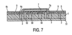
- FIG. 7 is a sectional view showing a schematic structure of a module component in embodiment 2 of the invention.
- FIG. 8 is a sectional view showing a schematic structure of a module component in embodiment 3 of the invention.
- FIG. 9 is a sectional view showing a molding method of a chip component in embodiment 4 of the invention.
- FIG. 10 is a perspective view showing a structure of molded component formed by the molding method.
- FIG. 11 is a sectional view showing an application example of module component employing a molded component in embodiment 5 of the invention.
- FIG. 12 ( a ) is a sectional view showing a structure of multi-layer substrate embedding electronic components in a prior art
- FIG. 12 ( b ) is its equivalent circuit diagram.
- FIG. 1 ( a ) is a sectional view at line I-I′ showing a schematic structure of a module component in embodiment 1 of the invention
- FIG. 1 ( b ) is a top view of the component.
- reference numeral 1 denotes a resin substrate.
- chip resistors 2 , chip capacitors 3 , and other chip components are inserted into penetration holes having the nearly same hole shapes as chip components, and their end electrodes and circuit wirings 4 a and 4 b formed on both sides of resin substrate 1 are electrically coupled to compose a desired electric circuit. They are held and reinforced between first auxiliary substrate 5 and second auxiliary substrate 6 .
- IC chip 7 and electronic components 8 that are hardly reduced in size are mounted on first auxiliary substrate 5 and are electrically coupled to wiring circuit 4 c and further to circuit wiring 4 a through conductor filling in through-holes 9 .
- Reference numeral 7 a denotes a molding resin
- 10 denotes an external electrode terminal on module component 11 .
- chip components to be inserted all conforms to 0603 (0.6 mm ⁇ 0.3 mm) of JIS (C-5201-8), and the height of resin substrate 1 is 0.6 mm to conform to this standard. Since the sizes of chip components are standardized, even if the circuit composition is changed, resin substrate 1 may be used commonly without changing its height, so that its versatility is very high.
- chip components to be inserted are resistors (R) and capacitors (C), but not limited to them.
- Coils (L), LC. CR and other composite components can be employed, and the same effects are obtained as far as the standardized chip components are employed.
- chip components of size of 1005 of JIS can be also employed.
- Chip components with various heights can be also employed, a circuit can be flexibly designed, and module components with a small size, multiple functions, and higher performance can thus be realized.
- FIG. 3 is a schematic diagram showing the state of chip components inserted in the penetration holes provided in the resin substrate, in which FIG. 3 ( a ) is a top view and FIG. 3 ( b ) is a sectional view.
- penetration holes (no reference numeral) having almost the same hole shapes as chip components are formed according to a matrix in resin substrate 21 , and chip resistors 22 and chip capacitors 23 are inserted therein.
- the penetration holes are arranged so that the chip components may be inserted and arranged while two sides of each chip component is aligned. But the penetration holes can be formed so that the centers of the chip components may be aligned, and the same effect is thus obtained.
- the penetration holes are formed regularly and precisely according to a matrix, it is very easy to insert chip components by machine. And as a result of enhancing a performance of an automatic inserting machine, the chip components may be further reduced in size, and the pitch of penetration holes may be narrowed.
- a desired circuit can be composed by: forming penetration holes according to the size of chip components to be inserted only in necessary positions depending on the circuit design and inserting a specific number of chip components.
- a desired circuit may be also composed by forming penetration holes in the entire matrix surface and inserting a specific number of chip components only in necessary positions depending on the circuit design with filling the remaining penetration holes with insulator or inserting insulators having a chip component size, i.e., dummy components.
- the resin substrate can be used commonly, and the circuit may be composed flexibly and easily changed only by changing the inserting positions and type of the chip components. And further, by employing the dummy components, they can be inserted automatically same as other chip components, and the production efficiency is thus notably enhanced.
- the hole shape of the penetration holes is not limited to the same shape as the chip components, but may be formed in circular, elliptical or polygonal shape denoted by reference numerals 24 a through 24 d in FIG. 4, as far as the shape is easy to hold positioning within the penetration hole. And by forming the holes in such shape, it is possible to insert chip components securely into the penetration hole even if the insertion angle of the chip component is deviated when inserting by machine for automation. By filling the gap between penetration hole and chip component with fixing member 24 made of thermosetting resin like epoxy resin, or by forming support part 26 for supporting the chip component by projecting a part of the penetration hole, the chip component can be securely supported and fixed in the penetration hole. And the reliability of connection of the circuit wiring and chip components disposed on the circuit board may be further enhanced.
- the shape of the penetration hole is not limited to a circular column, but may be tapered in such conical shape or Y-form shape as denoted by reference numerals 27 a through 27 c in FIG. 5 . And by tapering in such shape that the end of the chip component may reach to the bottom of the penetration hole, the opening at the chip-component-inserting-side of the penetration hole becomes wider, it is easier to insert chip components by machine, a position of the chip component can be automatically determined in the penetration hole, and the gap of the penetration hole and chip component may be smoothly filled up with fixing members. Outstanding merits can thus be obtained.
- an end of the chip component and a surface of the resin substrate are formed in different colors, it is easier to inspect a visual appearance, e.g. dropout of chip components, after inserting chip components into penetration holes.
- Resin substrate 31 of glass epoxy or Teflon of which both sides are lined with copper foil 32 (a: double-side-copper-lined substrate) is prepared.
- Through-holes 33 are formed by drill or laser to penetrate through both copper foils 32 (b: through-hole forming step), and non-electric copper plating is applied to conduct between both copper foils 32 (c: through-hole plating step).
- desired circuit wiring patterns 34 are formed on both sides of resin substrate 31 (d: pattern etching step), penetration holes 35 are formed for inserting chip components in specified positions according to a matrix (e: parts-inserting-hole forming step), and a specific number of such chip components as chip resistors 36 and chip capacitors 37 are inserted into specified penetration holes 35 (f: parts-inserting step).
- circuit wiring pattern 34 conductive resin, e.g. conductive adhesive material resin electrode material, are applied or printed on end electrodes 36 a and 37 a .
- connection electrodes are formed (g: connection-electrode forming step).
- viscous and adhesive pre-preg layer 41 which is formed with copper foil 40 on one side of auxiliary substrate 39 made of thermosetting resin like epoxy resin or phenol resin by heated and compressed in the condition of 180° C., 1 hour, and 30 kg/cm 2 (h: pre-preg layer forming step).
- resin substrate 31 is lower than chip components, and the total of resin substrate 31 including both copper foils 32 is higher than the chip components.
- the configuration is for reinforcing the connection of circuit wiring pattern 34 and end electrodes 36 a , 37 a of chip components. But configuration is not limited to above.
- Resin substrate 31 can be almost as high as the chip component, i.e., resin substrate 31 can be slightly higher than the chip component, or the total including both copper foils 32 can be slightly lower than the chip component.
- through-holes 42 are formed and filling with conductive material, and surface circuit wiring pattern 43 is formed by photolithography (i: surface layer pattern etching step). And an IC chip and other electronic components which is hardly reduced in size are mounted on the surface as shown in FIG. 1 . so that a module component having a desired circuit composition is completed (the process of mounting is not shown).
- first and second auxiliary substrates 4 , 5 are made of resin mainly composed of such thermosetting resin as epoxy resin or phenol resin. Thanks to a process at temperature as low as possible, an influence of heat treatment on chip components decreases. And without employing special chip components having excellent beat resistance, chip components can work in the specified resistance value and capacity, so that the circuit characteristics, functions and dimensional precision exactly as designed may be obtained.
- FIG. 7 is a sectional view showing a schematic structure of a module component in embodiment 2 of the invention, in which same elements as in embodiment 1 in FIG. 1 are identified with the same reference numerals, and their explanation is omitted.
- reference numeral 50 denotes a bypass capacitor, which is disposed immediately beneath the terminal of IC chip 7 and coupled through a shortest path. It is effective for reducing influence of noise in the wiring circuit which is often a problem in the conventional IC chip.
- Reference numeral 51 denotes a ground layer made of metal plate or copper foil, and the layer functions as a ground and cooling plate.
- bypass line 52 which is made of conductive material like copper or aluminum having excellent heat conductivity immediately beneath the terminal of IC chip 7 releases heat from the IC chip therethrough efficiently.
- ground layer 51 is directly formed on resin substrate 1 , but even when it is formed on second auxiliary substrate 6 shown in FIG.
- bypass line 52 is formed of such a conductive material as a copper chip having a chip component size, it can be inserted automatically in the same manner as other chip components. And working efficiency is substantially enhanced as compared with the operation of filing with conductive material.
- FIG. 8 is a sectional view showing a schematic structure of a module component in embodiment 3 of the invention, in which same elements as in embodiment 1 in FIG. 1 are identified with same reference numerals, and their explanation is omitted.
- reference numeral 53 denotes a printed-resistor formed on resin substrate 1 .
- the resister can be formed on circuit wiring 4 a without inserting a chip component in a penetration hole. After trimming it, first and second auxiliary substrates 5 , 6 can be laminated, which is very beneficial for reducing size and producing it efficiently.
- Reference numeral 54 denotes a laminated-capacitor. A capacitor having a low capacitance can be formed with electrode terminals 54 a , 54 b in circuit wirings 4 a , 4 b and dielectric constant of the substrate itself 54 c , so that it can be very effective for reducing the size.
- the penetration holes formed in the circuit board made of resin are disposed according to a specified rule, and a desired circuit is formed with putting a specific number of chip components therein.
- a module component can be formed without baking the chip components in/on the resin substrate, and the chip components work in specified values, and the circuit characteristics, functions and dimensional precision exactly as designed may thus be obtained stably.
- the penetration holes are disposed according to a specified rule, chip components can easily inserted into penetration holes automatically at high speed. And the technique is flexibly applicable even for a chip component having a small size, and moreover the circuit can be composed flexibly and changed easily only by changing an inserting position and a type of the chip component, and outstanding effects are obtained.
- module component of the invention Another manufacturing method of a module component of the invention will be explained below.
- the structure of the module component manufactured in the manufacturing method of the embodiment is substantially same as that of embodiment 1, i.e., shown in FIG. 1, and its description is omitted.
- the size of chip components to be molded in this embodiment all conforms to, same as in embodiment 1, 0603 (0.6 mm ⁇ 0.3 mm) of JIS (C-5201-8), and the height of resin substrate 1 is 0.6 mm to conform to this standard.
- the size of the chip component is standardized same as in embodiment 1, even if the circuit composition is changed, the height of resin substrate 1 is unchanged, and the versatility is very high.
- resin substrate 21 is formed where chip resistors 22 and chip capacitors 23 are molded according to a matrix, and the end electrodes are exposed.
- the chip components are arranged and molded so that the two sides of each chip component may be aligned in the diagram, but the same effect is obtained even if chip components are arranged and molded so that the center of each chip component may be aligned.
- the chip components are molded according to a matrix in the diagram, but it is not limited to this, except for disorderly scattering, same effect is obtained if the components are arranged in such a regular manner as concentric, radial or spiral profile.
- the chip components are inserted and arranged regularly and precisely according to a matrix in a molding die, a chip component is inserted automatically at high speed by a machine easily. As the performance of the automatic-inserting-machine is enhanced, the machine is applicable to downsizing of chip components and to narrowing of a pitch of chip components.
- Chip components are schematically molded in the entire surface of resin substrate 21 , and chip resistors 22 and chip capacitors 23 are molded alternately, but it is not limited to the configuration.
- Recesses are formed only at specified position in the molding die depending on the circuit design, and chip components of specific values are inserted and arranged, so that a desired circuit may be composed.
- Recesses are formed according to a matrix in a molding die, and chip components of specific values can be inserted, arranged, and molded only in necessary positions depending on the circuit design. Or a desired circuit may be formed also by inserting dummy components of same height, which components hardly influence to characteristics as module components, in the remaining recesses which are not filled with chip components.
- the die when matrix recesses formed in the molding die, the die can be used commonly, and the circuit can be changed flexibly and easily only by changing an inserting position and a type of a chip component. And further, by using the dummy components, chip components can always be molded in the same state, i.e., in the arranged state of chip components although there is a difference in the kind of components in recesses of matrix. And it can thus be molded precisely and stably.
- reference numeral 61 a denotes a first die, on which recesses 63 are formed for positioning and holding chip components 62 according to a matrix, and first chip components 62 are inserted and arranged in the recesses (a: chip component inserting step).
- recesses 63 in first die 61 a in such a taper shape as conical or Y-form shape (not shown), the opening area of the chip component-inserting-side becomes wider, a machine can insert the chip components more easily, chip components 62 can be positioned automatically in recesses 63 , and the gap of recesses 63 and chip components 62 can be filled up with resin smoothly. And outstanding merit is thus obtained.
- second die 61 b is moved into first die 61 a (b: primary molding-die-forming step). Resin 65 a is then put through filling ports 64 a , and a primary molding is performed (c: primary molding step). After the resin solidified, first die 61 a at inserting-side of chip component 62 is peeled off (d: chip-inserting-side-die peeling step). And third die 61 c is then moved so as to expose another end electrode 62 b of chip component 62 (e: secondary molding-die-forming step).
- Resin 65 b is put through filling ports 64 b , and secondary molding is performed (f: secondary molding step).
- Molded component 66 shown in FIG. 10 is obtained after peeling off second and third dies 61 b , 61 c and shaping the component (g: die-peeling, shaping step).
- thermosetting resin material such as epoxy resin or phenol resin
- an influence of a heat treatment on chip components decreases.
- the chip components work in the specified resistance value and capacity, so that the circuit characteristics, functions, and dimensional precision may be obtained exactly as designed.
- the module component having an excellent heat release and heat resistance is realized.
- the heat-release can be improved by containing at least one of Al 2 O 3 , SiC, Al 3 N 4 , and Si 3 N 4 as the filler in the resin.
- the heat resistance is enhanced by containing ceramic powder and/or SiO 2 as the filler in the resin.
- magnetic material such as ferrite in the resin, a module component resistant to an influence of noise may be realized.
- FIG. 11 is a sectional view showing a schematic structure of a module component in embodiment 5 of the invention, representing an application example of module component using module component 66 shown in FIG. 10 .
- FIG. 11 ( a ) illustrates an example of mounting molded component 66 on multi-layer substrate 70 .
- FIG. 11 ( b ) illustrates an example of burying molded component 66 in multi-layer substrate 70
- FIG. 11 ( c ) illustrates an example of forming molded component 66 smaller than IC chip 7 and burying it in multi-layer substrate 70 .
- Reference numerals 71 , 72 denote wiring patterns and through-holes provided in multi-layer substrate 70 , respectively. The same elements as in embodiment 4 are identified with the same reference numerals, and their explanation is omitted.
- chip capacitors of chip capacitors 62 function as bypass capacitors
- the ESR and ESL can be suppressed very small since the CPU and capacitors can be coupled directly, and it is thus applicable to higher speed in future.
- all or some of chip components 62 are designed to function as bypass capacitors, and when common electrodes are provided on both sides to cover and couple directly the end electrodes exposed therefrom with the CPU, it is applicable to a much higher speed operation.
- conductors having an excellent beat conductivity e.g. copper, aluminum
- they can function as a bypass line, and IC chip 7 can thus be cooled more efficiently.
- the substrate is formed by molding the resin, it is not necessary to heat chip components at high temperature, and the chip components work in specified values. And the circuit characteristics, functions, and dimensional precision may thus be obtained exactly and stably as designed. Since the chip components are disposed and molded with resin according to a specified rule, chip components to be inserted in the molding die automatically at a high speed are realized easily. The technique is flexibly applicable even if the size of the chip components is reduced, the circuit composition may be flexibly and easily changed only by changing an inserting position and a type of the chip components, and outstanding effect is obtained.
- module components described in embodiments 2 and 3 can be formed, and the module components formed with the method of embodiment 1 can be used in application examples in embodiment 5, which is evident and is not particularly explained herein.
- the chip components it is not required to heat the buried chip components at high temperature when forming module components, and the chip components work in specified values. And therefore, the circuit characteristics, functions, and dimensional precision may be obtained exactly and stably as designed. Since the chip components are disposed according to a specified rule, automatic and high speed insertion of chip components is easily realized. The technique is flexibly applicable even if the size of the chip components is reduced, and moreover, the circuit composition may be flexibly and easily changed only by changing the inserting position and type of the chip components.
Abstract
Description
Claims (15)
Priority Applications (2)
| Application Number | Priority Date | Filing Date | Title |
|---|---|---|---|
| US10/212,698 US6879493B2 (en) | 1999-04-16 | 2002-08-07 | Module component and method of manufacturing the same |
| US10/788,463 US7421781B2 (en) | 1999-04-16 | 2004-03-01 | Method of forming a module component having a plurality of penetration holes |
Applications Claiming Priority (5)
| Application Number | Priority Date | Filing Date | Title |
|---|---|---|---|
| JP10935299 | 1999-04-16 | ||
| JP11-109352 | 1999-04-16 | ||
| JP16790399 | 1999-06-15 | ||
| JP11-167903 | 1999-06-15 | ||
| PCT/JP2000/002333 WO2000063970A1 (en) | 1999-04-16 | 2000-04-11 | Module component and method of manufacturing the same |
Related Parent Applications (1)
| Application Number | Title | Priority Date | Filing Date |
|---|---|---|---|
| PCT/JP2000/002333 A-371-Of-International WO2000063970A1 (en) | 1999-04-16 | 2000-04-11 | Module component and method of manufacturing the same |
Related Child Applications (1)
| Application Number | Title | Priority Date | Filing Date |
|---|---|---|---|
| US10/212,698 Division US6879493B2 (en) | 1999-04-16 | 2002-08-07 | Module component and method of manufacturing the same |
Publications (1)
| Publication Number | Publication Date |
|---|---|
| US6806428B1 true US6806428B1 (en) | 2004-10-19 |
Family
ID=26449125
Family Applications (3)
| Application Number | Title | Priority Date | Filing Date |
|---|---|---|---|
| US09/719,631 Expired - Lifetime US6806428B1 (en) | 1999-04-16 | 2000-04-11 | Module component and method of manufacturing the same |
| US10/212,698 Expired - Lifetime US6879493B2 (en) | 1999-04-16 | 2002-08-07 | Module component and method of manufacturing the same |
| US10/788,463 Expired - Fee Related US7421781B2 (en) | 1999-04-16 | 2004-03-01 | Method of forming a module component having a plurality of penetration holes |
Family Applications After (2)
| Application Number | Title | Priority Date | Filing Date |
|---|---|---|---|
| US10/212,698 Expired - Lifetime US6879493B2 (en) | 1999-04-16 | 2002-08-07 | Module component and method of manufacturing the same |
| US10/788,463 Expired - Fee Related US7421781B2 (en) | 1999-04-16 | 2004-03-01 | Method of forming a module component having a plurality of penetration holes |
Country Status (4)
| Country | Link |
|---|---|
| US (3) | US6806428B1 (en) |
| EP (1) | EP1098368B1 (en) |
| JP (1) | JP3659167B2 (en) |
| WO (1) | WO2000063970A1 (en) |
Cited By (16)
| Publication number | Priority date | Publication date | Assignee | Title |
|---|---|---|---|---|
| US20040134681A1 (en) * | 2002-12-06 | 2004-07-15 | Norihito Tsukahara | Circuit board and its manufacturing method |
| US20040150966A1 (en) * | 2003-01-30 | 2004-08-05 | Chu-Chin Hu | Integrated library core for embedded passive components and method for forming electronic device thereon |
| US20050000728A1 (en) * | 2003-07-03 | 2005-01-06 | Shinko Electric Industries Co., Ltd. | Wiring board provided with a resistor and process for manufacturing the same |
| US20070025092A1 (en) * | 2005-08-01 | 2007-02-01 | Baik-Woo Lee | Embedded actives and discrete passives in a cavity within build-up layers |
| US20070166886A1 (en) * | 2003-09-18 | 2007-07-19 | Antti Iihola | Method for manufacturing an electronic module |
| US20080196930A1 (en) * | 2005-06-16 | 2008-08-21 | Imbera Electronics Oy | Method for Manufacturing a Circuit Board Structure, and a Circuit Board Structure |
| US20080202799A1 (en) * | 2007-02-26 | 2008-08-28 | Bhret Graydon | Embedding an electronic component between surfaces of a printed circuit board |
| US20080202801A1 (en) * | 2005-06-15 | 2008-08-28 | Imbera Electronics Oy | Circuit Board Structure and Method for Manufacturing a Circuit Board Structure |
| US20080261338A1 (en) * | 2004-06-15 | 2008-10-23 | Imbera Electronics Oy | Method For Manufacturing an Electronics Module Comprising a Component Electrically Connected to a Conductor-Pattern Layer |
| CN101355857B (en) * | 2007-07-25 | 2011-04-06 | Tdk株式会社 | Electronic component-embedded board and method of manufacturing the same |
| US8225499B2 (en) | 2005-06-16 | 2012-07-24 | Imbera Electronics Oy | Method for manufacturing a circuit board structure, and a circuit board structure |
| US20130082402A1 (en) * | 2005-02-18 | 2013-04-04 | Fujitsu Semiconductor Limited | Semiconductor device |
| US20140140026A1 (en) * | 2009-12-11 | 2014-05-22 | Samsung Electronics Co., Ltd. | Package substrate and semiconductor package having the same |
| US20150124451A1 (en) * | 2012-05-07 | 2015-05-07 | Osram Gmbh | Mounting support for solid-state light radiation sources and light source therefor |
| CN105845641A (en) * | 2015-02-02 | 2016-08-10 | 英飞凌科技奥地利有限公司 | Electronic component |
| US20180132356A1 (en) * | 2015-08-11 | 2018-05-10 | Murata Manufacturing Co., Ltd. | Method for manufacturing capacitor built-in substrate |
Families Citing this family (42)
| Publication number | Priority date | Publication date | Assignee | Title |
|---|---|---|---|---|
| WO2001063991A1 (en) | 2000-02-25 | 2001-08-30 | Ibiden Co., Ltd. | Multilayer printed wiring board and method for producing multilayer printed wiring board |
| KR20030060898A (en) | 2000-09-25 | 2003-07-16 | 이비덴 가부시키가이샤 | Semiconductor element, method of manufacturing semiconductor element, multi-layer printed circuit board, and method of manufacturing multi-layer printed circuit board |
| PL355404A1 (en) * | 2002-08-08 | 2004-02-09 | Advanced Digital Broadcast Ltd. | Pronted circuit board with electronic components to be fitted on a pronted circuit board and method of fitting electronic components on printed circuit board |
| DE10252308B3 (en) * | 2002-11-11 | 2004-04-29 | Schweizer Electronic Ag | Semi-finished product for making circuit board, has battery or accumulator element with temperature- and pressure-resistance matching manufacturing parameters fixed in opening in no-conductor region |
| WO2005008733A2 (en) * | 2003-07-14 | 2005-01-27 | Avx Corporation | Modular electronic assembly and method of making |
| JP4506303B2 (en) * | 2003-08-29 | 2010-07-21 | 株式会社デンソー | Electronic control unit |
| KR100583252B1 (en) * | 2003-12-29 | 2006-05-24 | 엘지.필립스 엘시디 주식회사 | The organic electro-luminescence device and method for fabricating of the same |
| US20050207133A1 (en) * | 2004-03-11 | 2005-09-22 | Mark Pavier | Embedded power management control circuit |
| TW200603694A (en) * | 2004-05-15 | 2006-01-16 | Kalu K Vasoya | Printed wiring board with conductive constraining core including resin filled slots |
| US7301105B2 (en) * | 2004-08-27 | 2007-11-27 | Stablcor, Inc. | Printed wiring boards possessing regions with different coefficients of thermal expansion |
| WO2006099554A2 (en) * | 2005-03-15 | 2006-09-21 | C-Core Technologies, Inc. | Manufacturing process: how to construct constraining core material into printed wiring board |
| USRE45637E1 (en) | 2005-08-29 | 2015-07-28 | Stablcor Technology, Inc. | Processes for manufacturing printed wiring boards |
| US8101868B2 (en) | 2005-10-14 | 2012-01-24 | Ibiden Co., Ltd. | Multilayered printed circuit board and method for manufacturing the same |
| JP3942190B1 (en) * | 2006-04-25 | 2007-07-11 | 国立大学法人九州工業大学 | Semiconductor device having double-sided electrode structure and manufacturing method thereof |
| US7570493B2 (en) * | 2006-11-16 | 2009-08-04 | Sony Ericsson Mobile Communications | Printed circuit board with embedded circuit component |
| KR100861618B1 (en) * | 2007-03-02 | 2008-10-07 | 삼성전기주식회사 | Printed circuit board for improving tolerance of embedded capacitors, and process for manufacturing the same |
| JP4518113B2 (en) | 2007-07-25 | 2010-08-04 | Tdk株式会社 | Electronic component built-in substrate and manufacturing method thereof |
| KR100867150B1 (en) * | 2007-09-28 | 2008-11-06 | 삼성전기주식회사 | Printed circuit board with embedded chip capacitor and method for embedding chip capacitor |
| JP5101240B2 (en) * | 2007-10-25 | 2012-12-19 | 日本特殊陶業株式会社 | Board component built-in wiring board |
| JP5112005B2 (en) * | 2007-10-25 | 2013-01-09 | 日本特殊陶業株式会社 | Wiring board with built-in plate-shaped component and manufacturing method thereof |
| JP2009135391A (en) * | 2007-11-02 | 2009-06-18 | Denso Corp | Electronic device and method of manufacturing the same |
| US8045333B2 (en) | 2008-01-14 | 2011-10-25 | Rosemount Inc. | Intrinsically safe compliant circuit element spacing |
| US8125766B2 (en) * | 2008-06-13 | 2012-02-28 | Kemet Electronics Corporation | Concentrated capacitor assembly |
| CN102415224A (en) * | 2009-05-04 | 2012-04-11 | R&D电路股份有限公司 | Method and apparatus for improving power and loss for interconect configurations |
| US8304888B2 (en) * | 2009-12-22 | 2012-11-06 | Fairchild Semiconductor Corporation | Integrated circuit package with embedded components |
| US8654538B2 (en) * | 2010-03-30 | 2014-02-18 | Ibiden Co., Ltd. | Wiring board and method for manufacturing the same |
| US8764371B2 (en) * | 2010-07-29 | 2014-07-01 | The Heil Co. | Scale based load limiting for refuse vehicles |
| CN103492794A (en) | 2010-08-13 | 2014-01-01 | 任恩奭 | Inlay sheet, inlay sheet manufacturing method, and antenna |
| US8760847B2 (en) | 2010-11-30 | 2014-06-24 | Pratt & Whitney Canada Corp. | Low inductance capacitor assembly |
| JP2012164952A (en) * | 2011-01-20 | 2012-08-30 | Ibiden Co Ltd | Wiring board with built-in electronic component and method of manufacturing the same |
| JP2013038374A (en) * | 2011-01-20 | 2013-02-21 | Ibiden Co Ltd | Wiring board and manufacturing method of the same |
| WO2013008552A1 (en) * | 2011-07-13 | 2013-01-17 | イビデン株式会社 | Wiring board incorporating electronic component, and method for manufacturing wiring board incorporating electronic component |
| KR20130051708A (en) * | 2011-11-10 | 2013-05-21 | 삼성전기주식회사 | Semiconductor package and method for manufacturing the same |
| JP5955023B2 (en) * | 2012-02-23 | 2016-07-20 | 京セラ株式会社 | Printed wiring board with built-in component and manufacturing method thereof |
| JP2014150128A (en) * | 2013-01-31 | 2014-08-21 | Denso Corp | Electronic device |
| KR20150144587A (en) * | 2014-06-17 | 2015-12-28 | 삼성전기주식회사 | Substrate with electronic device embedded therein and manufacturing method thereof |
| US9332632B2 (en) | 2014-08-20 | 2016-05-03 | Stablcor Technology, Inc. | Graphene-based thermal management cores and systems and methods for constructing printed wiring boards |
| WO2016189609A1 (en) * | 2015-05-25 | 2016-12-01 | オリンパス株式会社 | Three-dimensional wiring board and method for manufacturing three-dimensional wiring board |
| US9837484B2 (en) * | 2015-05-27 | 2017-12-05 | STATS ChipPAC Pte. Ltd. | Semiconductor device and method of forming substrate including embedded component with symmetrical structure |
| US9673173B1 (en) * | 2015-07-24 | 2017-06-06 | Altera Corporation | Integrated circuit package with embedded passive structures |
| WO2018063279A1 (en) * | 2016-09-30 | 2018-04-05 | Intel Corporation | Vertical embedded component in a printed circuit board blind hole |
| JP7249907B2 (en) * | 2019-08-08 | 2023-03-31 | 新光電気工業株式会社 | Wiring board manufacturing method and laminated structure |
Citations (19)
| Publication number | Priority date | Publication date | Assignee | Title |
|---|---|---|---|---|
| US3142783A (en) * | 1959-12-22 | 1964-07-28 | Hughes Aircraft Co | Electrical circuit system |
| US3290756A (en) | 1962-08-15 | 1966-12-13 | Hughes Aircraft Co | Method of assembling and interconnecting electrical components |
| US3480836A (en) | 1966-08-11 | 1969-11-25 | Ibm | Component mounted in a printed circuit |
| US3536565A (en) * | 1967-09-14 | 1970-10-27 | Burroughs Corp | Method of making an electrical terminal board assembly |
| JPS56125891A (en) | 1980-03-10 | 1981-10-02 | Alps Electric Co Ltd | Method of mounting chip part on printed board |
| JPS56174883U (en) | 1980-05-27 | 1981-12-23 | ||
| JPS5930549Y2 (en) | 1980-04-11 | 1984-08-31 | 日立電子株式会社 | printed board |
| JPS63169798A (en) | 1987-01-07 | 1988-07-13 | 株式会社村田製作所 | Multilayer ceramic board with built-in electronic parts |
| US4933808A (en) * | 1989-05-11 | 1990-06-12 | Westinghouse Electric Corp. | Solderless printed wiring board module and multi-module assembly |
| US4979076A (en) | 1989-06-30 | 1990-12-18 | Dibugnara Raymond | Hybrid integrated circuit apparatus |
| US5027253A (en) * | 1990-04-09 | 1991-06-25 | Ibm Corporation | Printed circuit boards and cards having buried thin film capacitors and processing techniques for fabricating said boards and cards |
| US5034260A (en) | 1987-07-02 | 1991-07-23 | Canon Kabushiki Kaisha | Ceramic and circuit substrate and electronic circuit substrate by use thereof |
| JPH0432780Y2 (en) | 1986-05-14 | 1992-08-06 | ||
| US5280192A (en) * | 1990-04-30 | 1994-01-18 | International Business Machines Corporation | Three-dimensional memory card structure with internal direct chip attachment |
| US5309324A (en) | 1991-11-26 | 1994-05-03 | Herandez Jorge M | Device for interconnecting integrated circuit packages to circuit boards |
| JPH08228066A (en) | 1995-02-21 | 1996-09-03 | Kokusai Electric Co Ltd | Electronic-part loading substrate and manufacture thereof |
| US5875100A (en) * | 1996-05-31 | 1999-02-23 | Nec Corporation | High-density mounting method and structure for electronic circuit board |
| US5874770A (en) | 1996-10-10 | 1999-02-23 | General Electric Company | Flexible interconnect film including resistor and capacitor layers |
| US6180881B1 (en) | 1998-05-05 | 2001-01-30 | Harlan Ruben Isaak | Chip stack and method of making same |
Family Cites Families (24)
| Publication number | Priority date | Publication date | Assignee | Title |
|---|---|---|---|---|
| US3134930A (en) | 1961-11-17 | 1964-05-26 | Electro Optical Systems Inc | Microminiature circuitry |
| US3266125A (en) * | 1962-11-13 | 1966-08-16 | Douglas Aircraft Co Inc | Method for making electrical circuit modules |
| GB1249108A (en) * | 1967-10-02 | 1971-10-06 | Electrosil Ltd | Electric circuit assemblies |
| US3486836A (en) * | 1968-05-27 | 1969-12-30 | Perkin Elmer Corp | Heated chamber burners |
| JPS56174833U (en) | 1980-05-28 | 1981-12-23 | ||
| US4440972A (en) * | 1981-03-31 | 1984-04-03 | Rogers Corporation | Miniaturized bus bar with capacitors and method of making same |
| JPS5930549A (en) | 1982-08-12 | 1984-02-18 | Konishiroku Photo Ind Co Ltd | Copying device |
| US4722914A (en) | 1984-05-30 | 1988-02-02 | Motorola Inc. | Method of making a high density IC module assembly |
| US4748537A (en) * | 1986-04-24 | 1988-05-31 | Rogers Corporation | Decoupling capacitor and method of formation thereof |
| US4768286A (en) * | 1986-10-01 | 1988-09-06 | Eastman Christensen Co. | Printed circuit packaging for high vibration and temperature environments |
| JPH0744320B2 (en) * | 1989-10-20 | 1995-05-15 | 松下電器産業株式会社 | Resin circuit board and manufacturing method thereof |
| JP2737362B2 (en) | 1990-05-29 | 1998-04-08 | 松下電器産業株式会社 | Electric quantity storage device |
| US5185690A (en) * | 1991-10-16 | 1993-02-09 | Miller Mark L | High dielectric constant sheet material |
| US5259110A (en) * | 1992-04-03 | 1993-11-09 | International Business Machines Corporation | Method for forming a multilayer microelectronic wiring module |
| JPH05343855A (en) * | 1992-06-08 | 1993-12-24 | Cmk Corp | Multilayer printed wiring board and manufacture thereof |
| US5353498A (en) * | 1993-02-08 | 1994-10-11 | General Electric Company | Method for fabricating an integrated circuit module |
| US5306670A (en) * | 1993-02-09 | 1994-04-26 | Texas Instruments Incorporated | Multi-chip integrated circuit module and method for fabrication thereof |
| US5479076A (en) | 1994-06-07 | 1995-12-26 | Eastman Kodak Company | Current mode restart circuit for a dc arc lamp |
| US5819394A (en) * | 1995-02-22 | 1998-10-13 | Transition Automation, Inc. | Method of making board matched nested support fixture |
| US5689091A (en) * | 1996-09-19 | 1997-11-18 | Vlsi Technology, Inc. | Multi-layer substrate structure |
| US5981314A (en) * | 1996-10-31 | 1999-11-09 | Amkor Technology, Inc. | Near chip size integrated circuit package |
| JP3726985B2 (en) * | 1996-12-09 | 2005-12-14 | ソニー株式会社 | Manufacturing method of electronic parts |
| US6159676A (en) * | 1997-12-05 | 2000-12-12 | Eastman Kodak Company | Chemical sensitization of large tabular grain emulsions |
| JP3322199B2 (en) * | 1998-01-06 | 2002-09-09 | 株式会社村田製作所 | Multilayer ceramic substrate and method of manufacturing the same |
-
2000
- 2000-04-11 JP JP2000613003A patent/JP3659167B2/en not_active Expired - Fee Related
- 2000-04-11 US US09/719,631 patent/US6806428B1/en not_active Expired - Lifetime
- 2000-04-11 EP EP00915469A patent/EP1098368B1/en not_active Expired - Lifetime
- 2000-04-11 WO PCT/JP2000/002333 patent/WO2000063970A1/en active Application Filing
-
2002
- 2002-08-07 US US10/212,698 patent/US6879493B2/en not_active Expired - Lifetime
-
2004
- 2004-03-01 US US10/788,463 patent/US7421781B2/en not_active Expired - Fee Related
Patent Citations (19)
| Publication number | Priority date | Publication date | Assignee | Title |
|---|---|---|---|---|
| US3142783A (en) * | 1959-12-22 | 1964-07-28 | Hughes Aircraft Co | Electrical circuit system |
| US3290756A (en) | 1962-08-15 | 1966-12-13 | Hughes Aircraft Co | Method of assembling and interconnecting electrical components |
| US3480836A (en) | 1966-08-11 | 1969-11-25 | Ibm | Component mounted in a printed circuit |
| US3536565A (en) * | 1967-09-14 | 1970-10-27 | Burroughs Corp | Method of making an electrical terminal board assembly |
| JPS56125891A (en) | 1980-03-10 | 1981-10-02 | Alps Electric Co Ltd | Method of mounting chip part on printed board |
| JPS5930549Y2 (en) | 1980-04-11 | 1984-08-31 | 日立電子株式会社 | printed board |
| JPS56174883U (en) | 1980-05-27 | 1981-12-23 | ||
| JPH0432780Y2 (en) | 1986-05-14 | 1992-08-06 | ||
| JPS63169798A (en) | 1987-01-07 | 1988-07-13 | 株式会社村田製作所 | Multilayer ceramic board with built-in electronic parts |
| US5034260A (en) | 1987-07-02 | 1991-07-23 | Canon Kabushiki Kaisha | Ceramic and circuit substrate and electronic circuit substrate by use thereof |
| US4933808A (en) * | 1989-05-11 | 1990-06-12 | Westinghouse Electric Corp. | Solderless printed wiring board module and multi-module assembly |
| US4979076A (en) | 1989-06-30 | 1990-12-18 | Dibugnara Raymond | Hybrid integrated circuit apparatus |
| US5027253A (en) * | 1990-04-09 | 1991-06-25 | Ibm Corporation | Printed circuit boards and cards having buried thin film capacitors and processing techniques for fabricating said boards and cards |
| US5280192A (en) * | 1990-04-30 | 1994-01-18 | International Business Machines Corporation | Three-dimensional memory card structure with internal direct chip attachment |
| US5309324A (en) | 1991-11-26 | 1994-05-03 | Herandez Jorge M | Device for interconnecting integrated circuit packages to circuit boards |
| JPH08228066A (en) | 1995-02-21 | 1996-09-03 | Kokusai Electric Co Ltd | Electronic-part loading substrate and manufacture thereof |
| US5875100A (en) * | 1996-05-31 | 1999-02-23 | Nec Corporation | High-density mounting method and structure for electronic circuit board |
| US5874770A (en) | 1996-10-10 | 1999-02-23 | General Electric Company | Flexible interconnect film including resistor and capacitor layers |
| US6180881B1 (en) | 1998-05-05 | 2001-01-30 | Harlan Ruben Isaak | Chip stack and method of making same |
Cited By (37)
| Publication number | Priority date | Publication date | Assignee | Title |
|---|---|---|---|---|
| US7376318B2 (en) | 2002-12-06 | 2008-05-20 | Matsushita Electric Industrial Co., Ltd. | Circuit board and its manufacturing method |
| US20070114058A1 (en) * | 2002-12-06 | 2007-05-24 | Norihito Tsukahara | Circuit board and its manufacturing method |
| US20040134681A1 (en) * | 2002-12-06 | 2004-07-15 | Norihito Tsukahara | Circuit board and its manufacturing method |
| US7180749B2 (en) * | 2002-12-06 | 2007-02-20 | Matsushita Electric Industrial Co., Ltd. | Circuit board and its manufacturing method |
| US20040150966A1 (en) * | 2003-01-30 | 2004-08-05 | Chu-Chin Hu | Integrated library core for embedded passive components and method for forming electronic device thereon |
| US7190592B2 (en) * | 2003-01-30 | 2007-03-13 | Phoenix Precision Technology Corporation | Integrated library core for embedded passive components and method for forming electronic device thereon |
| US20050000728A1 (en) * | 2003-07-03 | 2005-01-06 | Shinko Electric Industries Co., Ltd. | Wiring board provided with a resistor and process for manufacturing the same |
| US20070166886A1 (en) * | 2003-09-18 | 2007-07-19 | Antti Iihola | Method for manufacturing an electronic module |
| US10798823B2 (en) | 2003-09-18 | 2020-10-06 | Imberatek, Llc | Method for manufacturing an electronic module and electronic module |
| US11716816B2 (en) | 2003-09-18 | 2023-08-01 | Imberatek, Llc | Method for manufacturing an electronic module and electronic module |
| US7696005B2 (en) * | 2003-09-18 | 2010-04-13 | Imbera Electronics Oy | Method for manufacturing an electronic module in an installation base |
| US20100188823A1 (en) * | 2003-09-18 | 2010-07-29 | Antti Iihola | Method for Manufacturing an Electronic Module |
| US9232658B2 (en) | 2003-09-18 | 2016-01-05 | Ge Embedded Electronics Oy | Method for manufacturing an electronic module |
| US20080261338A1 (en) * | 2004-06-15 | 2008-10-23 | Imbera Electronics Oy | Method For Manufacturing an Electronics Module Comprising a Component Electrically Connected to a Conductor-Pattern Layer |
| US8240032B2 (en) * | 2004-06-15 | 2012-08-14 | Imbera Electronics Oy | Method for manufacturing an electronics module comprising a component electrically connected to a conductor-pattern layer |
| US20130082402A1 (en) * | 2005-02-18 | 2013-04-04 | Fujitsu Semiconductor Limited | Semiconductor device |
| US9076789B2 (en) | 2005-02-18 | 2015-07-07 | Socionext Inc. | Semiconductor device having a high frequency external connection electrode positioned within a via hole |
| US20080202801A1 (en) * | 2005-06-15 | 2008-08-28 | Imbera Electronics Oy | Circuit Board Structure and Method for Manufacturing a Circuit Board Structure |
| US20080196930A1 (en) * | 2005-06-16 | 2008-08-21 | Imbera Electronics Oy | Method for Manufacturing a Circuit Board Structure, and a Circuit Board Structure |
| US9622354B2 (en) | 2005-06-16 | 2017-04-11 | Ge Embedded Electronics Oy | Method for manufacturing a circuit board structure |
| US8225499B2 (en) | 2005-06-16 | 2012-07-24 | Imbera Electronics Oy | Method for manufacturing a circuit board structure, and a circuit board structure |
| US8581109B2 (en) | 2005-06-16 | 2013-11-12 | Imbera Electronics Oy | Method for manufacturing a circuit board structure |
| US8240033B2 (en) | 2005-06-16 | 2012-08-14 | Imbera Electronics Oy | Method for manufacturing a circuit board |
| US11792941B2 (en) | 2005-06-16 | 2023-10-17 | Imberatek, Llc | Circuit board structure and method for manufacturing a circuit board structure |
| US11134572B2 (en) | 2005-06-16 | 2021-09-28 | Imberatek, Llc | Circuit board structure and method for manufacturing a circuit board structure |
| US8335084B2 (en) * | 2005-08-01 | 2012-12-18 | Georgia Tech Research Corporation | Embedded actives and discrete passives in a cavity within build-up layers |
| US20070025092A1 (en) * | 2005-08-01 | 2007-02-01 | Baik-Woo Lee | Embedded actives and discrete passives in a cavity within build-up layers |
| US7782629B2 (en) * | 2007-02-26 | 2010-08-24 | Flextronics Ap, Llc | Embedding an electronic component between surfaces of a printed circuit board |
| US20080202799A1 (en) * | 2007-02-26 | 2008-08-28 | Bhret Graydon | Embedding an electronic component between surfaces of a printed circuit board |
| CN101355857B (en) * | 2007-07-25 | 2011-04-06 | Tdk株式会社 | Electronic component-embedded board and method of manufacturing the same |
| US20140140026A1 (en) * | 2009-12-11 | 2014-05-22 | Samsung Electronics Co., Ltd. | Package substrate and semiconductor package having the same |
| US9030838B2 (en) * | 2009-12-11 | 2015-05-12 | Samsung Electronics Co., Ltd. | Package substrate and semiconductor package having the same |
| US20150124451A1 (en) * | 2012-05-07 | 2015-05-07 | Osram Gmbh | Mounting support for solid-state light radiation sources and light source therefor |
| CN105845641B (en) * | 2015-02-02 | 2019-11-12 | 英飞凌科技奥地利有限公司 | Electronic building brick |
| US9553051B2 (en) * | 2015-02-02 | 2017-01-24 | Infineon Technologies Austria Ag | Electronic component |
| CN105845641A (en) * | 2015-02-02 | 2016-08-10 | 英飞凌科技奥地利有限公司 | Electronic component |
| US20180132356A1 (en) * | 2015-08-11 | 2018-05-10 | Murata Manufacturing Co., Ltd. | Method for manufacturing capacitor built-in substrate |
Also Published As
| Publication number | Publication date |
|---|---|
| US20040165361A1 (en) | 2004-08-26 |
| JP3659167B2 (en) | 2005-06-15 |
| US6879493B2 (en) | 2005-04-12 |
| EP1098368A4 (en) | 2007-08-15 |
| EP1098368A1 (en) | 2001-05-09 |
| US7421781B2 (en) | 2008-09-09 |
| US20020186552A1 (en) | 2002-12-12 |
| WO2000063970A1 (en) | 2000-10-26 |
| EP1098368B1 (en) | 2011-12-21 |
Similar Documents
| Publication | Publication Date | Title |
|---|---|---|
| US6806428B1 (en) | Module component and method of manufacturing the same | |
| US6948944B2 (en) | Wiring board with built-in electronic component and method for producing the same | |
| US5220488A (en) | Injection molded printed circuits | |
| EP2066161A1 (en) | Method for manufacturing substrate with built-in component and substrate with built-in component | |
| US6281446B1 (en) | Multi-layered circuit board and method of manufacturing the same | |
| US5898991A (en) | Methods of fabrication of coaxial vias and magnetic devices | |
| US6891258B1 (en) | Interposer providing low-inductance decoupling capacitance for a packaged integrated circuit | |
| US5541567A (en) | Coaxial vias in an electronic substrate | |
| JP4720462B2 (en) | Flexible circuit board and manufacturing method thereof | |
| US9839132B2 (en) | Component-embedded substrate | |
| US20150213946A1 (en) | Printed wiring board | |
| US20060152329A1 (en) | Conductive polymer device and method of manufacturing same | |
| CN104575938A (en) | Coil component, manufacturing method thereof, coil component-embedded substrate, and voltage adjustment module having the same | |
| KR920007010A (en) | Chip-type HF magnetic coil device and manufacturing method thereof | |
| US10002710B2 (en) | Ceramic multilayer wiring substrate and module including the same | |
| EP1951009B1 (en) | Printed circuit board | |
| US6563210B2 (en) | Parallel plane substrate | |
| EP0424796A2 (en) | Injection molded printed circuits | |
| JP2005191100A (en) | Semiconductor board and its manufacturing method | |
| CN115553075A (en) | Method for producing a circuit board and circuit board with at least one embedded electronic component | |
| US20230343685A1 (en) | Core substrate and interposer | |
| US9736939B2 (en) | Printed circuit board and method of manufacturing printed circuit board | |
| US20230337363A1 (en) | Method for producing a printed circuit board, and printed circuit board having at least one embedded electronic component | |
| KR20160034168A (en) | Printed circuit board and manufacturing method thereof |
Legal Events
| Date | Code | Title | Description |
|---|---|---|---|
| AS | Assignment |
Owner name: MATSUSHITA ELECTRIC INDUSTRIAL CO., LTD., JAPAN Free format text: ASSIGNMENT OF ASSIGNORS INTEREST;ASSIGNORS:KIMURA, SUZUSHI;HIMORI, TSUYOSHI;HASHIMOTO, KOJI;REEL/FRAME:011534/0394 Effective date: 20010206 |
|
| STCF | Information on status: patent grant |
Free format text: PATENTED CASE |
|
| FEPP | Fee payment procedure |
Free format text: PAYOR NUMBER ASSIGNED (ORIGINAL EVENT CODE: ASPN); ENTITY STATUS OF PATENT OWNER: LARGE ENTITY |
|
| FPAY | Fee payment |
Year of fee payment: 4 |
|
| FPAY | Fee payment |
Year of fee payment: 8 |
|
| FEPP | Fee payment procedure |
Free format text: PAYER NUMBER DE-ASSIGNED (ORIGINAL EVENT CODE: RMPN); ENTITY STATUS OF PATENT OWNER: LARGE ENTITY Free format text: PAYOR NUMBER ASSIGNED (ORIGINAL EVENT CODE: ASPN); ENTITY STATUS OF PATENT OWNER: LARGE ENTITY |
|
| FPAY | Fee payment |
Year of fee payment: 12 |