US6801989B2 - Method and system for adjusting the timing offset between a clock signal and respective digital signals transmitted along with that clock signal, and memory device and computer system using same - Google Patents
Method and system for adjusting the timing offset between a clock signal and respective digital signals transmitted along with that clock signal, and memory device and computer system using same Download PDFInfo
- Publication number
- US6801989B2 US6801989B2 US09/896,030 US89603001A US6801989B2 US 6801989 B2 US6801989 B2 US 6801989B2 US 89603001 A US89603001 A US 89603001A US 6801989 B2 US6801989 B2 US 6801989B2
- Authority
- US
- United States
- Prior art keywords
- signal
- command
- phase
- circuit
- clock
- Prior art date
- Legal status (The legal status is an assumption and is not a legal conclusion. Google has not performed a legal analysis and makes no representation as to the accuracy of the status listed.)
- Expired - Fee Related, expires
Links
Images


Classifications
-
- G—PHYSICS
- G11—INFORMATION STORAGE
- G11C—STATIC STORES
- G11C29/00—Checking stores for correct operation ; Subsequent repair; Testing stores during standby or offline operation
- G11C29/02—Detection or location of defective auxiliary circuits, e.g. defective refresh counters
- G11C29/028—Detection or location of defective auxiliary circuits, e.g. defective refresh counters with adaption or trimming of parameters
-
- G—PHYSICS
- G06—COMPUTING; CALCULATING OR COUNTING
- G06F—ELECTRIC DIGITAL DATA PROCESSING
- G06F13/00—Interconnection of, or transfer of information or other signals between, memories, input/output devices or central processing units
- G06F13/14—Handling requests for interconnection or transfer
- G06F13/16—Handling requests for interconnection or transfer for access to memory bus
- G06F13/1668—Details of memory controller
- G06F13/1689—Synchronisation and timing concerns
-
- G—PHYSICS
- G11—INFORMATION STORAGE
- G11C—STATIC STORES
- G11C29/00—Checking stores for correct operation ; Subsequent repair; Testing stores during standby or offline operation
- G11C29/02—Detection or location of defective auxiliary circuits, e.g. defective refresh counters
-
- G—PHYSICS
- G11—INFORMATION STORAGE
- G11C—STATIC STORES
- G11C29/00—Checking stores for correct operation ; Subsequent repair; Testing stores during standby or offline operation
- G11C29/04—Detection or location of defective memory elements, e.g. cell constructio details, timing of test signals
- G11C29/50—Marginal testing, e.g. race, voltage or current testing
- G11C29/50012—Marginal testing, e.g. race, voltage or current testing of timing
Definitions
- the present invention relates generally to semiconductor memories and other integrated circuit devices, and is directed, more particularly, to synchronizing digital signals being transferred over buses interconnecting such devices.
- ROMs read-only memories
- SRAM static random access memory
- Processors generally operate at a relatively high speed. Processors such as the Pentium III® and Pentium 4® microprocessors are currently available that operate at clock speeds of at least 400 MHz. However, the remaining components of existing computer systems, with the exception of SRAM cache, are not capable of operating at the speed of the processor. For this reason, the system memory devices, as well as the input devices, output devices, and data storage devices, are not coupled directly to the processor bus. Instead, the system memory devices are generally coupled to the processor bus through a memory controller, bus bridge or similar device, and the input devices, output devices, and data storage devices are coupled to the processor bus through a bus bridge. The memory controller allows the system memory devices to operate at a lower clock frequency that is substantially lower than the clock frequency of the processor.
- the bus bridge allows the input devices, output devices, and data storage devices to operate at a substantially lower frequency.
- a processor having a 1 GHz clock frequency may be mounted on a mother board having a 133 MHz clock frequency for controlling the system memory devices and other components.
- Access to system memory is a frequent operation for the processor.
- much effort has been devoted to increasing the operating speed of system memory devices.
- DRAMs dynamic random access memories
- SDRAMs synchronous dynamic random access memories
- SDRAMs cannot be connected directly to the processor bus, but instead must interface with the processor bus through a memory controller, bus bridge, or similar device.
- the disparity between the operating speed of the processor and the operating speed of SDRAMs continues to limit the speed at which processors may complete operations requiring access to system memory.
- synchronous link architecture the system memory may be coupled to the processor either directly through the processor bus or through a memory controller.
- synchronous link memory devices receive command packets that include both control and address information. The synchronous link memory device then outputs or receives data on a data bus that may be coupled directly to the data bus portion of the processor bus.
- the computer system 10 includes a processor 12 having a processor bus 14 coupled through a memory controller 18 and system memory bus 23 to three packetized or synchronous link dynamic random access memory (“SLDRAM”) devices 16 a-c .
- the computer system 10 also includes one or more input devices 20 , such as a keypad or a mouse, coupled to the processor 12 through a bus bridge 22 and an expansion bus 24 , such as an industry standard architecture (“ISA”) bus or a peripheral component interconnect (“PCI”) bus.
- the input devices 20 allow an operator or an electronic device to input data to the computer system 10 .
- One or more output devices 30 are coupled to the processor 12 to display or otherwise output data generated by the processor 12 .
- the output devices 30 are coupled to the processor 12 through the expansion bus 24 , bus bridge 22 and processor bus 14 .
- Examples of output devices 24 include printers and a video display units.
- One or more data storage devices 38 are coupled to the processor 12 through the processor bus 14 , bus bridge 22 , and expansion bus 24 to store data in or retrieve data from storage media (not shown). Examples of storage devices 38 and storage media include fixed disk drives floppy disk drives, tape cassettes and compact-disk read-only memory drives.
- the processor 12 sends a data transfer command via the processor bus 14 to the memory controller 18 , which, in turn, communicates with the memory devices 16 a-c via the system memory bus 23 by sending the memory devices 16 a-c command packets that contain both control and address information.
- Data is coupled between the memory controller 18 and the memory devices 16 a-c through a data bus portion of the system memory bus 23 .
- data is transferred from the SLDRAMs 16 a-c over the memory bus 23 to the memory controller 18 which, in turn, transfers the data over the processor 14 to the processor 12 .
- the processor 12 transfers write data over the processor bus 14 to the memory controller 18 which, in turn, transfers the write data over the system memory bus 23 to the SLDRAMs 16 a-c .
- the computer system 10 also includes a number of other components and signal lines that have been omitted from FIG. 1 in the interests of brevity.
- the memory devices 16 a-c also receive a master clock signal to provide internal timing signals, a data clock signal clocking data into and out of the memory device 16 , and a FLAG signal signifying the start of a command packet.
- a typical command packet CA ⁇ 0:39> for an SLDRAM is shown in FIG. 2 and is formed by 4 packet words CA ⁇ 0:9>, each of which contains 10 bits of data. As will be explained in more detail below, each packet word CA ⁇ 0:9> is applied on a command-address bus CA including 10 lines CA0-CA9.
- the four packet words CA ⁇ 0:9> comprising a command packet CA ⁇ 0:39> are designated PW 1 -PW 4 .
- the first packet word PW 1 contains 7 bits of data identifying the packetized DRAM 16 a-c that is the intended recipient of the command packet.
- each of the packetized DRAMs is provided with a unique ID code that is compared to the 7 ID bits in the first packet word PW 1 . Thus, although all of the packetized DRAMs 16 a-c will receive the command packet, only the packetized DRAM 16 a-c having an ID code that matches the 7 ID bits of the first packet word PW 1 will respond to the command packet.
- the remaining 3 bits of the first packet word PW 1 as well as 3 bits of the second packet word PW 2 comprise a 6 bit command. Typical commands are read and write in a variety of modes, such as accesses to pages or banks of memory cells.
- the remaining 7 bits of the second packet word PW 2 and portions of the third and fourth packet words PW 3 and PW 4 comprise a 20 bit address specifying a bank, row and column address for a memory transfer or the start of a multiple bit memory transfer. In one embodiment, the 20 bit address is divided into 3 bits of bank address, 10 bits of row address, and 7 bits of column address.
- the command packet shown in FIG. 2 is composed of 4 packet words PW 1 -PW 4 each containing up to 10 bits, it will be understood that a command packet may contain a lesser or greater number of packet words, and each packet word may contain a lesser or greater number of bits.
- the memory device 16 a is shown in block diagram form in FIG. 3 .
- Each of the memory devices 16 a-c includes a clock generator circuit 40 that receives a command clock signal CCLK and generates a large number of other clock and timing signals to control the timing of various operations in the memory device 16 a .
- the memory device 16 a also includes a command buffer 46 and an address capture circuit 48 which receive an internal clock signal ICLK, a command packet CA ⁇ 0:9> on a 10 bit command-address bus CA, and a terminal 52 receiving a FLAG signal.
- a memory controller (not shown) or other device normally transmits the command packet CA ⁇ 0:9> to the memory device 16 a in synchronism with the command clock signal CCLK.
- the command packet CA ⁇ 0:39> which generally includes four 10-bit packet words PW 1 -PW 4 , contains control and address information for each memory transfer.
- the FLAG signal identifies the start of a command packet, and also signals the start of an initialization sequence.
- the command buffer 46 receives the command packet from the command-address bus CA, and compares at least a portion of the command packet to identifying data from an ID register 56 to determine if the command packet is directed to the memory device 16 a or some other memory device 16 b , c. If the command buffer 46 determines that the command is directed to the memory device 16 a , it then provides the command to a command decoder and sequencer 60 .
- the command decoder and sequencer 60 generates a large number of internal control signals to control the operation of the memory device 16 a during a memory transfer.
- the address capture circuit 48 also receives the command packet from the command-address bus CA and outputs a 20-bit address corresponding to the address information in the command packet.
- the address is provided to an address sequencer 64 , which generates a corresponding 3-bit bank address on bus 66 , a 10-bit row address on bus 68 , and a 7-bit column address on bus 70 .
- the row and column addresses are processed by row and column address paths, as will be described in more detail below.
- the SLDRAM 16 a shown in FIG. 3 largely avoids this problem by using a plurality of memory banks 80 , in this case eight memory banks 80 a-h . After a read from one bank 80 a , the bank 80 a can be precharged while the remaining banks 80 b-h are being accessed. Each of the memory banks 80 a-h receives a row address from a respective row latch/decoder/driver 82 a-h .
- All of the row latch/decoder/drivers 82 a-h receive the same row address from a predecoder 84 which, in turn, receives a row address from either a row address register 86 or a refresh counter 88 as determined by a multiplexer 90 .
- a predecoder 84 which, in turn, receives a row address from either a row address register 86 or a refresh counter 88 as determined by a multiplexer 90 .
- only one of the row latch/decoder/drivers 82 a-h is active at any one time as determined by bank control logic 94 as a function of a bank address from a bank address register 96 .
- the column address on bus 70 is applied to a column latch/decoder 100 , which supplies I/O gating signals to an I/O gating circuit 102 .
- the I/O gating circuit 102 interfaces with columns of the memory banks 80 a-h through sense amplifiers 104 .
- Data is coupled to or from the memory banks 80 a-h through the sense amps 104 and I/O gating circuit 102 to a data path subsystem 108 which includes a read data path 110 and a write data path 112 .
- the read data path 110 includes a read latch 120 that stores data from the I/O gating circuit 102 .
- the read latch 120 In the memory device 16 a shown in FIG. 3, 64 bits of data are stored in the read latch 120 .
- the read latch then provides four 16-bit data words to an output multiplexer 122 that sequentially supplies each of the 16-bit data words to a read FIFO buffer 124 . Successive 16-bit data words are clocked through the read FIFO buffer 124 in response to a clock signal RCLK generated by the clock generator 40 .
- the FIFO buffer 124 sequentially applies the 16-bit data words to a driver circuit 128 which, in turn, applies the 16-bit data words to a data bus DQ forming part of the processor bus 14 (see FIG. 1 ).
- the FIFO buffer 124 also applies two data clock signals DCLK 0 and DCLK 1 to the driver circuit 128 which, in turn, applies the data clock signals DCLK 0 and DCLK 1 on respective data clock lines 132 and 133 .
- the data clocks DCLK 0 and DCLK 1 enable a device, such as the memory controller 18 , reading data on the data bus DQ to be synchronized with the data.
- Particular bits in the command portion of the command packet CA0-CA9 determine which of the two data clocks DCLK 0 and DCLK 1 is applied by the driver circuit 128 .
- the data clocks DCLK 0 and DCLK 1 are differential clock signals, each including true and complementary signals, but for ease of explanation, only one signal for each clock is illustrated and described.
- the write data path 112 includes a receiver buffer 140 coupled to the data bus 130 .
- the receiver buffer 140 sequentially applies 16-bit data words from the data bus DQ to four input registers 142 , each of which is selectively enabled by a signal from a clock generator circuit 144 .
- the clock generator circuit 144 generates these enable signals responsive to the selected one of the data clock signals DCLK 0 and DCLK 1 .
- the memory controller or processor determines which data clock DCLK 0 or DCLK 1 will be utilized during a write operation using the command portion of a command packet applied to the memory device 16 a .
- the memory controller or other device normally transmits the data to the memory device 16 a in synchronism with the selected one of the data clock signals DCLK 0 and DCLK 1 .
- the clock generator 144 is programmed during initialization to adjust the timing of the clock signal applied to the input registers 142 relative to the selected one of the data clock signals DCLK 0 and DCLK 1 so that the input registers 142 can capture the write data at the proper times.
- the input registers 142 In response to the selected data clock DCLK 0 or DCLK 1 , the input registers 142 sequentially store four 16-bit data words and combine them into one 64-bit data word applied to a write FIFO buffer 148 .
- the write FIFO buffer 148 is clocked by a signal from the clock generator 144 and an internal write clock WCLK to sequentially apply 64-bit write data to a write latch and driver 150 .
- the write latch and driver 150 applies the 64-bit write data to one of the memory banks 80 a-h through the I/O gating circuit 102 and the sense amplifiers 104 .
- an important goal of the synchronous link architecture is to allow data transfer between a processor or memory controller and a memory device to occur at a significantly faster rate.
- the rate of data transfer increases, it becomes more difficult to maintain synchronization of signals transmitted between the memory controller 18 and the memory device 16 a .
- the command packet CA ⁇ 0:39> is normally transmitted from the memory controller 18 to the memory device 16 a in synchronism with the command clock signal CCLK, and the read and write data are normally transferred between the memory controller 18 and the memory device 16 a in synchronism with the selected one of the data clock signals DCLK 0 and DCLK 1 .
- the command packet CA ⁇ 0:39> may not arrive at the memory device 16 a in synchronism with the command clock signal CCLK, and write and read data may not arrive at the memory device 16 a and memory controller 18 , respectively, in synchronism with the selected one of the data clock signals DCLK 0 and DCLK 1 .
- these signals may loose synchronism once they are coupled to circuits within these respective devices.
- this synchronism may be lost over time during normal operation of the memory device 16 a . Loss in synchronism may result from a variety of factors, including temperature variations in the environment in which the memory device 16 a is operating, variations in the supply voltage applied to the memory device, and drift in operating parameters of components within the memory device.
- synchronization of the clock signals CCLK, DCLK 0 , and DCLK 1 is being used to mean the adjusting of the timing of respective internal clock signals derived from these respective external clock signals so the internal clock signals can be used to latch corresponding digital signals at the proper times.
- the command clock signal CCLK is synchronized when the timing of the internal clock signal ICLK relative to the command clock signal CCLK causes packet words CA ⁇ 0:9> to be latched at the proper times.
- the memory controller 18 applies a test bit pattern and (FIG. 1) places the memory device 16 a in a command and write data synchronization mode.
- synchronization circuitry within the memory device 16 a (not shown in FIG. 3) detects the applied bit pattern, places the device in the synchronization mode, and thereafter generates the necessary control signals to control components within the memory device to synchronize the clock signals CCLK, DCLK 0 , and DCLK 1 from the controller 18 .
- the data clock signals DCLK 0 and DCLK 1 must similarly be synchronized for read operations between the memory controller 18 and memory device 16 a.
- data transfer includes all digital signals transferred to and from the memory device 16 a , and thus includes signals on the CA and DQ busses as well as the FLAG signal. As the data transfer rate increases, it becomes more difficult to maintain the required timing between signals transmitted between the memory device 16 a and the memory controller 18 .
- the command packet CA ⁇ 0:39> is normally transmitted to the memory device 16 a in synchronization with the command clock signal CCLK, and the data is normally transmitted to the memory device 16 a in synchronization with the selected one of the data clock signals DCLK 0 and DCLK 1 .
- the command packet words CA ⁇ 0:9> may not arrive at the memory device 16 a in synchronization with the command clock signal CCLK, and the data packet words may not arrive at the memory device 16 a in synchronization with the selected data clock signal DCLK 0 or DCLK 1 .
- phase shift of respective internal clock signals derived from these respective external clock signals must be adjusted so the internal clock signals can be used to latch corresponding packet words at optimum times.
- the phase shift of the internal clock signal ICLK relative to the command clock signal CCLK must be adjusted so that all command signals CA ⁇ 0>-CA ⁇ 9> in each packet word CA ⁇ 0:9> are latched at the optimum time.
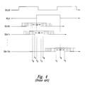
- the duration for which each signal CA ⁇ 0>-CA ⁇ 9> in a packet word CA ⁇ 0:9> is valid decreases by a corresponding amount, as will be understood by one skilled in the art. More specifically, the data window or “eye” DE for each of the DQ ⁇ 0>-DQ ⁇ 15> signals decreases at higher data transfer rates. As understood by one skilled in the art, the data eye DE for each of the DQ ⁇ 0>-DQ ⁇ 9> signals defines the actual duration that each signal is valid after timing skew of the signal is considered. The timing skew of the DQ ⁇ 0>-DQ ⁇ 9> signals arises from a variety of timing errors such as loading on the lines of the DQ bus and the physical lengths of such lines. FIG.
- FIG. 4 is a timing diagram illustrating the data eyes DE for a number of the DQ ⁇ 0>-DQ ⁇ 9> signals.
- the solid lines indicate the ideal DQ ⁇ 0>, DQ ⁇ 1>, and DQ ⁇ 9> signals, and the dashed lines indicate the worst case potential time skew for each of these signals.
- the data eyes DE of the DQ ⁇ 0>, DQ ⁇ 1>, and DQ ⁇ 9> signals are defined by time intervals t 0 -t 3 , t 1 -t 4 , and t 5 -t 7 , respectively.
- the signals DQ ⁇ 0> and DQ ⁇ 15> are not both valid at the memory device 16 a at the same time so the packet word DQ ⁇ 0:15> cannot be successfully captured responsive to the RCLK signal.
- the transition of the RCLK signal at time t 2 could successfully capture the DQ ⁇ 0> and DQ ⁇ 1> signals, but not the DQ ⁇ 15> signal, and, conversely, the transition of the RCLK signal at time t 6 could successfully capture the DQ ⁇ 15> signal but not the DQ ⁇ 0> and DQ ⁇ 1> signals, both of which have already gone invalid at time t 6 .
- a method adaptively adjusts respective timing offsets of a plurality of digital signals relative to a clock signal being output along with the digital signals to enable a circuit receiving the digital signals successfully to each of the digital signals responsive to the clock signal.
- the method includes storing in a respective storage circuit associated with each digital signal a corresponding phase command.
- the phase command defines a particular timing offset between the corresponding digital signal and the clock signal.
- the clock signal is output along with each digital signal having the timing offset defined by the corresponding phase command.
- the digital signals are captured responsive to the clock signal and evaluated to determine if each digital signal was successfully captured.
- a phase adjustment command is generated to adjust the value of each phase command.
- the operations of outputting the clock signal through generating a phase adjustment command are repeated for a plurality of phase adjustment commands for each digital signal.
- a phase command that causes the digital signal to be successfully captured is then selected, and the selected phase command is stored in the storage circuit associated with the digital signal.
- a read synchronization circuit adaptively adjusts respective timing offsets of a plurality of digital signals applied on respective signal terminals and an external data clock signal to enable an external device to latch the digital signals responsive to the external data clock signal.
- the read synchronization circuit includes a plurality of latch circuits, each latch circuit including an input, an output coupled to a respective signal terminal, and a clock terminal. Each latch circuit stores a signal applied on the input and providing the stored signal on the signal terminal responsive to a clock signal applied on the clock terminal.
- a plurality of phase command registers store phase commands with each register being associated with at least one of the latch circuits.
- a clock generation circuit is coupled to latch circuits and the phase command registers and generates a plurality of internal clock signals and the external data clock signal responsive to a read clock signal. Each internal clock signal and the external clock signal has a respective phase shift relative to the read clock signal.
- the clock generation circuit selects one of the internal clock signals for each latch circuit in response to the associated phase command and applies the selected internal clock signal to the clock terminal of the latch circuit to place digital signals on the corresponding signal terminal with a timing offset determined by the phase shift of the selected internal clock signal.
- a control circuit is coupled to the clock generation circuit and the phase command registers and operates in response to a synchronization command to apply synchronization digital signals on the inputs of the latch circuits and to adjust the respective timing offsets between the external data clock signal and the synchronization digital signals output by each latch circuit by adjusting the respective values of the phase commands.
- the circuit stores final phase commands in each phase command register that allow the synchronization digital signals to be successfully captured responsive to the external data clock signal.
- the read synchronization circuit may be utilized in a variety of different types of integrated circuits, including packetized memory devices such as SLDRAMs, nonpacketized devices such as double-data-rate synchronous dynamic random access memories (DDR SDRAMs), and alternative memory architectures having alternative clocking topologies.
- FIG. 1 is a block diagram of a conventional computer system including a plurality of packetized memory devices.
- FIG. 2 is diagram showing a typical command packet received by the packetized memory devices of FIG. 1 .
- FIG. 3 is a block diagram of a conventional packetized memory device in the computer system of FIG. 1 .
- FIG. 4 is a timing diagram illustrating the effect of timing skews on capturing respective data signals on the data bus at high data transfer rates.
- FIG. 5 is block diagram of a read synchronization system for a packetized memory device according to one embodiment of the present invention.
- FIG. 6 is a timing diagram illustrating the operation of the system of FIG. 5 in adjusting the respective timing offsets of several data bits relative to a data clock signal to allow the memory controller (FIG. 5) to successfully capture all data bits in response to the data clock signal.
- FIG. 7 is a functional block diagram illustrating a memory system including components of the read synchronization system of FIG. 5 according to another embodiment of the present invention.
- FIG. 5 is a functional block diagram of a read synchronization system 400 including a memory controller 402 and packetized memory device 404 according to one embodiment of the present invention.
- the memory controller 402 applies command packets CA ⁇ 0:39> and FLAG bits to the memory device 404 over the command-address bus CA and FLAG line, respectively, and transfers data packet words D ⁇ 0:15> on the data bus DQ.
- the memory controller 402 clocks the received data packet words D ⁇ 0:15> into the controller responsive to one of the data clocks DCLK 0 and DCLK 1 .
- the memory controller 402 Prior to performing read operations, the memory controller 402 places the memory device 404 in a read synchronization mode of operation and adjusts the timing offset of respective bits DQ ⁇ 0>-DQ ⁇ 15> in the data packet words D ⁇ 0:15> relative to the data clock signals DCLK 0 and DCLK 1 to synchronize the data clock signals for use during normal read operations, as will be explained in more detail below.
- synchronization of the data clock signals DCLK 0 and DCLK 1 as described herein means the adjustment of the timing offset of respective bits D ⁇ 0>-D ⁇ 15> in the data packet words D ⁇ 0:15> relative to the data clock signals DCLK 0 and DCLK 1 such that the memory controller 402 can successfully capture the data packet words D ⁇ 0:15> responsive to the data clock signals DCLK 0 and DCLK 1 , as will be discussed in more detail below.
- certain details are set forth to provide a sufficient understanding of the present invention. However, it will be clear to one skilled in the art that the invention may be practiced without these particular details. In other instances, well-known circuits, control signals, timing protocols, and software operations have not been shown in detail in order to avoid unnecessarily obscuring the invention.
- the command buffer and address capture circuit 46 (FIG. 3) latches packet words CA ⁇ 0:9> and FLAG bits applied on the respective command-address bus CA and FLAG line as previously described with reference to FIG. 3.
- a command decoder and sequencer 408 receives the latched command packet CA ⁇ 0:39> and FLAG bits from the command buffer and address capture circuit 46 and generates a plurality of control signals 410 to control the operation of various components within the memory device 404 in response to the latched command packet CA ⁇ 0:39> and FLAG signals.
- the command decoder and sequencer 408 generates a phase adjust command word PHADJCMD ⁇ 0:Y> in response to a phase adjustment command that is applied on the command-address bus CA and latched by the command buffer and address capture circuit 46 , as will be described in more detail below.
- An up/down phase counter-controller 416 latches the phase adjust command word PHADJCMD from the command decoder and sequencer 408 and operates in response to the latched phase adjust command word to develop a phase command word CMDPH ⁇ 0:3> and to store the developed phase command word in one of a plurality of phase command registers 434 A-P, as will be explained in more detail below.
- the latched CMDPH ⁇ 0:3> word stored in the registers 434 A-P are designated as phase command words CMDPH 0 ⁇ 0:3>-CMDPH 15 ⁇ 0:3>, respectively.
- a plurality of multiplexers 436 A-P receive the CMDPH 0 ⁇ 0:3>-CMDPH 15 ⁇ 0:3> words, respectively, stored in the registers 434 A-P, and further receive a plurality of clock signals 438 A-N from a delay-locked loop circuit 418 on respective inputs.
- the delay-locked loop circuit 418 develops the plurality of clock signals 438 A-N in response to the RCLK signal, with the clock signals 438 A-N having phase shifts, designated ⁇ 1 - ⁇ N , respectively, relative to the RCLK signal.
- the delay-locked loop circuit 418 develops sixteen clock signals 434 A-N and maintains a phase shift of 180° between the clock signals 438 A and 438 N.
- Each multiplexer 436 A-P provides one of the applied clock signals 438 A-N on an output in response to the phase command word CMDPH 0 ⁇ 0:3>-CMDPH 15 ⁇ 0:3> applied from the corresponding register 434 A-P.
- the clock signals output by the multiplexers 436 A-P are designated data read clocks DRCLK 0 -DRCLK 15 , respectively, and are applied to clock respective read synchronization data bits RSDW ⁇ 0>-RSDW ⁇ 15> into a plurality of data latches 440 A-P.
- a read data pattern generator 424 generates the RSDW ⁇ 0>-RSDW ⁇ 15> bits, as will be discussed in more detail below.
- the latches 440 A-P store the applied RSDW ⁇ 0>-RSDW ⁇ 15> bits, respectively, and apply the stored bits through corresponding buffers 442 A-P as the data bits D ⁇ 0>-D ⁇ 15> on the data bus DQ.
- the DRCLK 0 -DRCLK 15 signals thus determine when each latch 440 A-P places the corresponding RSDW ⁇ 0>-RSDW ⁇ 15> bit onto the corresponding line of the data bus DQ relative to transitions of the RCLK signal.
- each DRCLK 0 -DRCLK 15 signal corresponds to one of the clock signals 438 A-N selected by the corresponding multiplexer 436 A-P responsive to the applied CMPDH 0 ⁇ 0:3>-CMDPH 15 ⁇ 0:3> word, and each clock signal 438 A-N has a defined phase shift relative to the RCLK signal as previously described.
- the memory device 404 further includes a data clock driver circuit 446 that generates the data clock signals DCLK 0 and DCLK 1 in response to the read clock signal RCLK. Although the two data clocks DCLK 0 , DCLK 1 are discussed in the described embodiments, only one data clock may be used in an alternative embodiment as will be understood by those skilled in the art.
- the read data pattern generator 424 generates successive 16-bit read synchronization data packet words RSDW ⁇ 0:15>, with respective bits RSDW ⁇ 0>-RSDW ⁇ 15> in each word being clocked into respective data latches 440 A-P in response the DCLK 0 -DCLK 15 signals.
- the 16-bit data packet words D ⁇ 0:15> corresponding to the data being accessed are successively output from the multiplexer 122 (FIG. 3) and are clocked into the data latches 440 A-P responsive to the DCLK 0 -DCLK 15 signals and thereafter applied through the buffers 442 A-P and onto the data bus DQ.
- FIG. 3 For ease of explanation and clarity of description, FIG.
- the driver circuit 446 outputs the DCLK 0 , DCLK 1 signals along with the RSDW ⁇ 0:15> words being successively placed on the data bus DQ during the read synchronization mode and outputs the selected one of the DCLK 0 , DCLK 1 signals along with the 16-bit data packet words being successively placed on the data bus DQ during the normal read mode.
- the read data pattern generator 424 may generate a variety of data patterns, and in one embodiment the read data pattern generator 424 generates a 15-bit repeating pseudo-random bit sequence as described in U.S.
- the memory controller 402 sequentially latches data words D ⁇ 0:15> applied on the data bus DQ by the memory device 404 in response to the selected DCLK 0 , DCLK 1 signal. For each bit in the latched D ⁇ 0:15> words, the memory controller 402 executes a synchronization process to determine whether the latched bit D ⁇ 0>-D ⁇ 15> was successfully captured in response to the selected one of the DCLK 0 , DCLK 1 signals. For example, the controller can generate an expected value for the bit D ⁇ 0>-D ⁇ 15> and compare the latched bit to the expected value. When the two bits are equal, the controller 402 determines the bit was successfully captured, and otherwise determines the capture was unsuccessful.
- the controller 402 then sends a phase adjustment command to the memory device 404 over the CA bus.
- the device 404 adjusts the timing offset between the selected DCLK 0 , DCLK 1 signal and the bit D ⁇ 0:15> being synchronized, and thereafter once again determines whether the bit is successfully captured.
- the memory controller 402 operates in the read synchronization mode in response to a predetermined condition.
- the memory controller 402 may operate in the read synchronization mode of operation as part of an initialization and synchronization procedure during which the memory controller 402 also synchronizes the command clock signal CCLK and the data clock signals DCLK 0 and DCLK 1 during write operations, and further performs other functions in initializing the memory device 404 .
- the memory controller 402 may operate in the read synchronization mode of operation after a predetermined time during normal operation of the memory controller and memory device 404 in order to periodically resynchronize the data clock signals DCLK 0 and DCLK 1 .
- phase adjustment commands After commencing operation in the read synchronization mode of operation, the memory controller 402 applies phase adjustment commands to the memory device 404 .
- Each phase adjustment command includes information identifying a particular memory device 404 and a particular bit D ⁇ 0>-D ⁇ 15> that is to be synchronized. contains information that is utilized by the memory device 404 to adjust the value of the phase command word CMDPH ⁇ 0:3> stored in a corresponding phase command register 434 A-P, as will be explained in more detail below.
- the phase adjustment command also selects one of the DCLK 0 , DCLK 1 signals with which each D ⁇ 0>-D ⁇ 15> bit is to be synchronized.
- the value of the CMDPH ⁇ 0:3> word adjusts the timing offset between the corresponding bit D ⁇ 0>-D ⁇ 15> and transitions of the selected data clock signal DCLK 0 and DCLK 1 , and in this way the memory controller 402 utilizes the phase adjustment commands to adjust this offset for each bit D ⁇ 0>-D ⁇ 15>.
- the command buffer and address capture circuit 46 latches the applied phase adjustment commands read in response to the ICLK signal as previously described with reference to FIG. 3, and outputs the latched command to the command decoder and sequencer 408 .
- the command decoder and sequencer 408 decodes the command portion of the applied phase adjustment command and thereafter generates the control signals 410 to place the memory device 404 in the read synchronization mode of operation.
- the up/down phase counter-controller 416 stores initial values for the CMDPH 0 -CMDPH 15 ⁇ 0:15> words in the phase command registers 434 A-P, and the read data pattern generator 424 begins sequentially applying the read synchronization data words RSDW ⁇ 0:15> to the data latches 440 A-P.
- the command decoder and sequencer 408 also generates the phase adjustment command word PHADJCMD ⁇ 0:Y> in response to the applied phase adjustment command from the controller 402 .
- the value of the generated phase adjustment command word PHADJCMD ⁇ 0:Y> is determined by the value of the phase adjustment command, and in this way the memory controller 402 controls the value of the phase adjustment command word PHADJCMD ⁇ 0:Y>.
- the PHADJ ⁇ 0:N> word contains information identifying a “selected” bit, which corresponds to the bit D ⁇ 0>-D ⁇ 15> on the data bus DQ that is being synchronized, and the PHADJCMD ⁇ 0:Y> word similarly contains information identifying the selected bit.
- the developed PHADJCMD ⁇ 0:Y> word is applied to the counter-controller 416 , which first examines the latched PHADJCMD ⁇ 0:Y> word to determine the selected bit and thereafter reads the current value of the phase command word CMDPH ⁇ 0:3> stored in the phase command register 434 A-P associated with the selected bit. For example, if the PHADJCMD ⁇ 0:Y> word identifies the bit D ⁇ 0>, the counter-controller 416 reads the value of the CMDPH 0 ⁇ 0:3> word stored in the phase command register 434 A.
- the counter-controller 416 After reading the value of CMDPH ⁇ 0:3> word stored in the selected phase command register 434 A-P, the counter-controller 416 generates a new value for the CMDPH ⁇ 0:3> word responsive to the PHADJCMD ⁇ 0:Y>.
- the PHADJCMD ⁇ 0:Y> word may contain information instructing the counter-controller 416 to increment or decrement the value of the read CMDPH ⁇ 0:3> word.
- the counter-controller 416 stores the new word in the appropriate phase command register 434 A-P. For example, if bit D ⁇ 0> is being synchronized, the counter-controller 416 stores the newly generated value for the CMDPH 0 ⁇ 0:3> word in the register 434 A.
- the counter-controller 416 can, alternatively, simply store an updated phase command word CMDPH ⁇ 0:3> in the appropriate register 434 A-P responsive to the PHADJCMD ⁇ 0:Y> word. In this way, the counter-controller 416 need not first read the CMDPH ⁇ 0:3> word stored in the register 413 A-P being updated.
- the counter-controller 416 can simultaneously adjust the values of the CMDPH 0 ⁇ 0:3>-CMDPH 15 ⁇ 0:3> words stored in the registers 434 A-P, respectively.
- the PHADJCMD ⁇ 0:Y> word includes information the counter-controller 416 uses in independently adjusting each of the CMDPH 0 ⁇ 0:3>-CMDPH 15 ⁇ 0:3> words.
- each multiplexer 436 A-P outputs a selected one of the clock signals 438 A-N as the corresponding DRCLK 0 -DRCLK 15 signal, with the selected clock signal being determined by the value of the CMDPH 0 -CMDPH 15 ⁇ 0:3> word applied to the multiplexer from the corresponding phase command register 434 A-P.
- the data bits RSDW ⁇ 0>-RSDW ⁇ 15> are clocked out of the data latches 440 A-P having respective timing offsets relative to the RCLK signal and thus relative to the DCLK 0 , DCLK 1 signals, with each timing offset being determined by the value of the CMDPH 0 -CMDPH 15 ⁇ 0:3> word store in the corresponding phase command register 434 A-P.
- the memory controller 402 latches applied D ⁇ 0:15> words responsive to the selected DCLK 0 , DCLK 1 signal, and then determines whether the bit D ⁇ 0>-D ⁇ 15> being synchronized in the latched word was successfully captured.
- the memory controller 402 compares the latched value of the bit D ⁇ 0>-D ⁇ 15> being synchronized applied data word D ⁇ 0:63> to the expected value for the bit and stores the result of the comparison.
- the Memory controller 402 thereafter generates a second phase adjustment command including an incremented phase value, and applies this new command to the memory device 404 .
- the command buffer and address capture circuit 46 once again latches the applied phase adjustment command and outputs the latched command to the command decoder and sequencer 408 .
- the command decoder and sequencer 408 applies a new PHADJCMD ⁇ 0:Y> word to the counter-controller 416 which, in turn, reads the current value of the selected CMDPH 0 ⁇ 0:3>-CMDPH 15 ⁇ 0:3> word and increments or decrements the current value to develop a new CMDPH 0 ⁇ 0:3>-CMDPH ⁇ 15> word.
- the counter-controller 416 then stores the new value of the CMDPH 0 ⁇ 0:3>-CMDPH ⁇ 15> word in the corresponding register 434 A-P.
- the RSDW ⁇ 0>-RSDW ⁇ 15> bits from the pattern generator 424 are clocked into the data latches 440 A-P responsive to the clock signals DRCLK 0 -DRCLK 15 , respectively, with each of these clock signals having an offset relative to the DCLK 0 , DCLK 1 signals as determined the current values of the CMDPH 0 ⁇ 0:3>-CMDPH 15 ⁇ 0:3> words.
- the RSDW ⁇ 0:15> words are thus clocked out of the data latches 440 A-P as the data initialization packet words D ⁇ 0:15> on the data bus DQ, each bit D ⁇ 0>-D ⁇ 15> having a timing offset relative to the selected DCLK 0 , DCLK 1 signal with the selected bit D ⁇ 0>-D ⁇ 15> currently being synchronized having a new timing offset as determined by the new value of the corresponding CMDPH 0 ⁇ 0:3>-CMDPH ⁇ 0:3> word.
- the memory controller 402 once again captures from the data bus DQ the data initialization packet words D ⁇ 0:15> having the new timing offset applied to the bit D ⁇ 0>-D ⁇ 15> being synchronized, compares the latched value to an expected value, and stores the result of this comparison.
- the memory controller 402 continues adjusting the value of the phase adjustment command and applying the adjusted commands to the memory device 404 in order to adjust the timing offset between the selected D ⁇ 0>-D ⁇ 15> bit and the selected data clock signal DCLK 0 , DCLK 1 .
- the memory controller 402 As the memory controller 402 adjusts the values of the phase adjustment commands, the memory controller stores a number of comparison results, each comparison result value corresponding to a particular value of the phase adjustment command (i.e., a particular timing offset of the selected bit D ⁇ 0>-D ⁇ 15> relative to the selected DCLK 0 and DCLK 1 signal). After a predetermined number of comparison results have been stored, the memory controller 402 executes a phase selection procedure to select a final phase adjustment command from among the phase adjustment commands that resulted in the successful capture of the selected bit D ⁇ 0>-D ⁇ 15> as indicated by the corresponding comparison result.
- a phase selection procedure to select a final phase adjustment command from among the phase adjustment commands that resulted in the successful capture of the selected bit D ⁇ 0>-D ⁇ 15> as indicated by the corresponding comparison result.
- the memory controller 402 stores sixteen comparison results, each corresponding to one of sixteen values for the phase adjustment command, and selects the final phase adjustment command from among the ones of the sixteen values that resulted in the successful capture of the selected D ⁇ 0>-D ⁇ 15> bit.
- One procedure that may be executed by the control circuit 406 in determining the final phase adjustment word PHADJ ⁇ 0:4> is described in more detail in U.S. Pat. No. 5,953,284 to Baker et al., entitled METHOD AND APPARATUS FOR ADAPTIVELY ADJUSTING THE TIMING OF A CLOCK SIGNAL USED TO LATCH DIGITAL SIGNALS, AND MEMORY DEVICE USING SAME, which issued Sep. 14, 1999 and which is incorporated herein by reference.
- the memory controller 402 After selecting the desired one of the phase adjustment commands, the memory controller 402 applies the selected phase adjustment command to the memory device 404 .
- the command buffer and address capture circuit 46 and command decoder and sequencer 408 in the memory device 404 then operate as previously described develop the selected PHADJCMD ⁇ 0:Y> word corresponding to the selected phase adjustment command.
- the counter-controller 416 receives the selected PHADJCMD ⁇ 0:Y> word, which includes information indicating that the word corresponds to the final selected value for the corresponding bit D ⁇ 0>-D ⁇ 15>.
- the counter-controller 416 In response to the selected PHADJCMD ⁇ 0:Y> word, the counter-controller 416 operates as previously described to update the value of the CMDPH 0 ⁇ 0:3>-CMDPH ⁇ 0:3> word stored in the register 434 A-P corresponding to the bit being synchronized to a final value as determined by the selected PHADJCMD ⁇ 0:Y> word. For example, if the D ⁇ 0> bit is being synchronized, the counter-controller 416 sets the value of the CMDPH 0 ⁇ 0:3> word stored in the register 434 A to a final value as determined by the selected PHADJCMD ⁇ 0:Y> word.
- the corresponding clock signal DRCLK 0 -DRCLK 15 signal has a phase relative to the read clock signal RCLK that is determined by the final phase command word, and this phase is utilized during normal read operations of the memory device 404 .
- This final phase command word CMDPH 0 ⁇ 0:3>-CMDPH 15 ⁇ 0:3> defines the timing offset between the selected DCLK 0 , DCLK 1 signal and the corresponding bit D ⁇ 0>-D ⁇ 15>.
- This timing offset is then used during normal read operations of the memory device 404 so that the memory controller 402 may successfully capture this bit in the data packet words D ⁇ 0:15> being transferred to the memory controller in response to read commands from the controller.
- the memory controller 402 control circuit 406 thereafter develops a data clock offset to edge align the second DCLK 0 , DCLK 1 signal with the selected data clock signal. That enables the controller 402 to successfully capture data bits D ⁇ 0>-D ⁇ 15> responsive to either DCLK 0 , DCLK 1 signal.
- the memory controller 402 After synchronizing both DCLK 0 , DCLK 1 signals for the selected bit D ⁇ 0>-D ⁇ 15>, the memory controller 402 develops a new phase adjustment command identifying the next bit D ⁇ 0>-D ⁇ 15> to be synchronized, and the memory controller 402 and memory device 404 thereafter operate in the same way as just described to synchronize the newly selected bit.
- the controller 402 and memory device 404 repeat this process for each of the bits D ⁇ 0>-D ⁇ 15> to independently synchronize each bit with the DCLK 0 , DCLK 1 signals.
- phase command registers 434 A-P store final phase command values CMDPH 0 ⁇ 0:3>-CMDPH 15 ⁇ 0:3> to define the respective timing offsets between the each bit D ⁇ 0>-D ⁇ 15> and the DCLK 0 , DCLK 1 signals.
- the exact process executed in synchronizing each D ⁇ 0>-D ⁇ 15> bit may be varied. For example each bit D ⁇ 0>-D ⁇ 15> may first be synchronized with the DCLK 0 signal, and then each synchronized with the DCLK 1 signal.
- a selected D ⁇ 0>-D ⁇ 15> bit may be synchronized with the DCLK 0 signal, then the next selected bit synchronized with the DCLK 0 , signal, and so on sequentially for all bits.
- respective D ⁇ 0>-D ⁇ 15> bits may be independently synchronized with the DCLK 0 , signal in parallel.
- the memory device 404 includes a shadow register 450 , which is indicated with dotted lines, coupled between the counter-controller 416 and the phase command registers 434 A-P.
- the shadow register 450 stores all the current CMDPH 0 - 15 ⁇ 0:3> words, and functions as a storage “pipeline” between the counter-controller 416 and the registers 434 A-P.
- the phase command registers 434 A-P will typically be located near the data latches 440 A-P and buffers 442 A-P, which will all be physically proximate the external data bus DQ terminals of the memory device 404 .
- the counter-controller 416 may not be located physically near the registers 434 A-P, thus causing the transfer of CMDPH 0 - 15 ⁇ 0:3> words between the registers and the counter-controller to be slowed down due to the physical lengths of the data lines interconnecting these two components, as will be appreciated by those skilled in the art. If the counter-controller 416 must wait until an updated CMDPH 0 - 15 ⁇ 0:3> word has been stored in the corresponding register 434 A-P, the operation of the system 400 may be slowed down due to the delay in transferring the words between the counter-controller and the registers.
- the counter-controller 416 can quickly update the value of one of the CMDPH 0 - 15 ⁇ 0:3> words responsive to a corresponding phase adjustment command word PHADJCMD ⁇ 0:Y> and thereafter begin processing a subsequent PHADJCMD ⁇ 0:Y> word.
- the shadow register 450 thereafter transfers the updated CMDPH 0 - 15 ⁇ 0:3> word to the proper register 434 A-P while the counter-controller 416 is processing the subsequent command word PHADJCMD ⁇ 0:Y>.
- FIG. 6 is a signal timing diagram that will be utilized to illustrate the relationship between the phase shift of the DRCLK 0 -DRCLK 15 signals relative to the RCLK signal as defined by the respective CMDPH 0 ⁇ 0:3>-CMDPH ⁇ 15> words, and also illustrates the corresponding timing offset between the DCLK 0 signal and respective bits D ⁇ 0>-D ⁇ 15> applied on the data bus DQ.
- the DCLK 0 signal which is generated by the drivers 446 in response to the RCLK signal, has the same phase as the RCLK signal.
- the DRCLK 0 signal has a phase shift ⁇ 1 relative to the DCLK 0 signal.
- the corresponding data bit D ⁇ 0> is placed on the data bus DQ have a timing offset t off1 relative to the rising edge of DCLK 0 signal at a time t 0 .
- the data bit D ⁇ 0> is offset by the time t off1 to enable the memory controller 402 to successfully latch the data bit in response to the DCLK 0 signal.
- the DRCLK 1 signal corresponding to the CMDPH 1 ⁇ 0:3> word has a phase shift ⁇ 2 relative to the DCLK 0 signal
- the corresponding data bit D ⁇ 1> has a timing offset t off2 relative to the rising edge of the DCLK 0 signal at the time to.
- the data bit D ⁇ 1> is applied on the data bus DQ at a time t 2 before the rising edge of the DCLK 0 signal at the time to.
- the third example illustrates the DRCLK 15 signal having a phase shift ⁇ 3 relative to the DCLK 0 signal
- the corresponding data D ⁇ 15> has a timing offset t off3 relative to the rising edge of the DCLK 0 signal at the time to.
- the data D ⁇ 15> is applied on the data bus DQ at a time t 3 before the rising edge of the DCLK 0 signal at the time to.
- the phase command words CMDPH 0 ⁇ 0:3>, CMDPH 1 ⁇ 0:3>, and CMDPH 15 ⁇ 0:3> are independently adjusted to thereby vary the phase shift of the DRCLK 0 -DRCLK 15 signals relative to the DCLK 0 signal.
- the timing offsets of the respective data bits D ⁇ 0>-D ⁇ 15> in each data packet D ⁇ 0:15> applied on the data bus DQ are adjusted relative to transitions of the DCLK 0 signal by an amount corresponding to the adjusted phase shifts.
- the procedure executed by the control circuit 406 in synchronizing the data clock signals DCLK 0 , DCLK 1 may vary.
- the control circuit 406 captures only one data packet D ⁇ 0:63> at each phase of the DRCLK 0 -DRCLK 15 signal corresponding to the bit D ⁇ 0>-D ⁇ 15> being synchronized.
- the control circuit 406 may perform a predetermined number of comparisons at each given phase of the DRCLK 0 -DRCLK 15 signal and timing offset of the corresponding D ⁇ 0>-D ⁇ 15> bit relative to the data clocks DCLK 0 and DCLK 1 .
- control circuit 406 may, for example, control components of the memory controller 402 so that eight data packets D ⁇ 0:63> are captured and compared at each phase of the DRCLK 0 -DRCLK 15 signals. When all eight of these comparisons indicate successful captures, the control circuit 406 stores a “1” indicating successful data capture at this phase. However, if any of the comparisons at a given phase indicates an unsuccessful capture, the control circuit 406 stores a “0” indicating failure at this phase. Once again, after sixteen, for example, results signals have been stored, the control circuit 406 determines the final phase adjustment word PHADJ ⁇ 0:4> and transfers this word to the memory device 404 .
- the memory device 404 then operates as previously described, applying the corresponding PHADJCMD ⁇ 0:Y> word to the counter-controller 416 which, in turn, stores the final phase command word CMDPH 0 ⁇ 0:3>-CMDPH 15 ⁇ 0:3> in the appropriate phase command register 434 A-P to thereby set the final phase of the corresponding DRCLK 0 -DRCLK 15 signal being adjusted.
- the synchronization system 400 may be used in a variety of different types of memory devices in addition to the SLDRAM devices described herein, such as in RAMBUS type memory devices and in double-data-rate synchronous dynamic random access memory devices (“DDR SDRAMs”).
- DDR SDRAMs double-data-rate synchronous dynamic random access memory devices
- the timing offsets of respective bits on the data bus DQ are adjusted with respect to a data strobe signal DQS, as will be appreciated by those skilled in the art.
- FIG. 7 is a functional block diagram illustrating a memory system 700 including memory devices 702 , 704 that include read synchronization circuits 703 , 705 according to another embodiment of the present invention.
- Each of the read synchronization circuits 703 , 705 includes components (not shown) of the read synchronization system 400 of FIG. 5, as will be discussed in more detail below.
- a clock generator 706 generates a system read clock signal RCLK that is applied to the memory devices 702 , 704 and is applied to a memory controller 708 .
- the memory device 702 , 704 being accessed supplies read data on a data bus DQ and the memory controller 708 latches the read data in response to the RCLK signal.
- the memory controller 708 supplies write data on the data bus DQ and applies a write clock signal WCLK to the memory devices 702 , 704 which, in turn, latch the write data in response to the write clock signal.
- the memory controller 708 applies command and address information to the memory devices 702 , 704 over a command bus CMD and also applies a command clock signal CCLK that the memory devices utilize to latch the applied command and address information.
- the command bus CMD may be a multiplexed bus including both command and address information when the memory devices 702 , 704 are packetized type memory devices such as SLDRAMs.
- the command bus CMD may include separate command and address busses when the memory devices 702 , 704 are non packetized type memory devices such as a DDR SDRAM.
- the memory controller 708 applies a write command on the CMD bus to the memory devices 702 , 704 which, in turn, latch the write command in response to the CCLK signal also applied by the memory controller.
- Each of the memory devices 702 , 704 decodes the latched command and determines whether it is the device being accessed.
- the memory controller 708 supplies write data on the DQ bus and the memory device 702 , 704 being accessed latches the supplied write data in response to the CCLK signal from the memory controller.
- the memory controller 708 applies the read command on the CMD bus to the memory devices 702 , 704 which, once again, latch and decode the read command.
- Each of the data bits on the DQ bus has a respective timing offset relative to the RCLK signal, with the timing offsets being determined during a read synchronization mode of operation.
- the respective timing offsets allow the memory controller 708 to successfully capture all read data bits supplied on the DQ bus during normal read operations.
- the circuits 703 , 705 operate in an analogous manner to components of the read synchronization system 400 of FIG. 5 .
- phase command CMDPH is stored in corresponding phase command register 434 A- 434 P (see FIG. 5) to define the timing offset between the data bit and the RCLK signal.
Abstract
Description
Claims (66)
Priority Applications (2)
| Application Number | Priority Date | Filing Date | Title |
|---|---|---|---|
| US09/896,030 US6801989B2 (en) | 2001-06-28 | 2001-06-28 | Method and system for adjusting the timing offset between a clock signal and respective digital signals transmitted along with that clock signal, and memory device and computer system using same |
| US10/686,118 US7159092B2 (en) | 2001-06-28 | 2003-10-14 | Method and system for adjusting the timing offset between a clock signal and respective digital signals transmitted along with that clock signal, and memory device and computer system using same |
Applications Claiming Priority (1)
| Application Number | Priority Date | Filing Date | Title |
|---|---|---|---|
| US09/896,030 US6801989B2 (en) | 2001-06-28 | 2001-06-28 | Method and system for adjusting the timing offset between a clock signal and respective digital signals transmitted along with that clock signal, and memory device and computer system using same |
Related Child Applications (1)
| Application Number | Title | Priority Date | Filing Date |
|---|---|---|---|
| US10/686,118 Continuation US7159092B2 (en) | 2001-06-28 | 2003-10-14 | Method and system for adjusting the timing offset between a clock signal and respective digital signals transmitted along with that clock signal, and memory device and computer system using same |
Publications (2)
| Publication Number | Publication Date |
|---|---|
| US20030005250A1 US20030005250A1 (en) | 2003-01-02 |
| US6801989B2 true US6801989B2 (en) | 2004-10-05 |
Family
ID=25405486
Family Applications (2)
| Application Number | Title | Priority Date | Filing Date |
|---|---|---|---|
| US09/896,030 Expired - Fee Related US6801989B2 (en) | 2001-06-28 | 2001-06-28 | Method and system for adjusting the timing offset between a clock signal and respective digital signals transmitted along with that clock signal, and memory device and computer system using same |
| US10/686,118 Expired - Fee Related US7159092B2 (en) | 2001-06-28 | 2003-10-14 | Method and system for adjusting the timing offset between a clock signal and respective digital signals transmitted along with that clock signal, and memory device and computer system using same |
Family Applications After (1)
| Application Number | Title | Priority Date | Filing Date |
|---|---|---|---|
| US10/686,118 Expired - Fee Related US7159092B2 (en) | 2001-06-28 | 2003-10-14 | Method and system for adjusting the timing offset between a clock signal and respective digital signals transmitted along with that clock signal, and memory device and computer system using same |
Country Status (1)
| Country | Link |
|---|---|
| US (2) | US6801989B2 (en) |
Cited By (52)
| Publication number | Priority date | Publication date | Assignee | Title |
|---|---|---|---|---|
| US20020049936A1 (en) * | 2000-07-31 | 2002-04-25 | Vadim Gutnik | Clock distribution circuits and methods of operating same that use multiple clock circuits connected by phase detector circuits to generate and synchronize local clock signals |
| US20030233608A1 (en) * | 2002-06-18 | 2003-12-18 | Roy Aninda K. | Round-robin updating for high speed i/o parallel interfaces |
| US20040123060A1 (en) * | 2002-06-27 | 2004-06-24 | Amit Bodas | Method and apparatus for dynamic timing of memory interface signals |
| US20050172095A1 (en) * | 2004-01-29 | 2005-08-04 | Micron Technology, Inc. | Dual edge command in DRAM |
| US20050219919A1 (en) * | 2004-03-31 | 2005-10-06 | Micron Technology, Inc. | Reconstruction of signal timing in integrated circuits |
| US20060067157A1 (en) * | 2004-09-30 | 2006-03-30 | Hermann Ruckerbauer | Memory system with two clock lines and a memory device |
| US20060103444A1 (en) * | 2004-11-15 | 2006-05-18 | Hynix Semiconductor Inc. | Data output circuit of memory device |
| US20060203603A1 (en) * | 2004-12-23 | 2006-09-14 | Infineon Technologies Ag | Memory arrangement and method for processing data |
| US20070041253A1 (en) * | 2005-03-22 | 2007-02-22 | Mediatek Inc. | Methods and systems for generating latch clock used in memory reading |
| US20070061536A1 (en) * | 2004-03-31 | 2007-03-15 | Micron Technology, Inc. | Reconstruction of signal timing in integrated circuits |
| US20070143031A1 (en) * | 2003-08-30 | 2007-06-21 | Istech Co., Ltd. | Method of analyzing a bio chip |
| US20070240630A1 (en) * | 2002-06-24 | 2007-10-18 | Leonard Robert T | One hundred millimeter single crystal silicon carbide water |
| US20080037353A1 (en) * | 2006-07-31 | 2008-02-14 | Metaram, Inc. | Interface circuit system and method for performing power saving operations during a command-related latency |
| US20080181043A1 (en) * | 2007-01-31 | 2008-07-31 | Rajesh Sundaram | Configurable device ID in non-volatile memory |
| US20080225630A1 (en) * | 2004-08-04 | 2008-09-18 | Micron Technology, Inc. | Method and apparatus for initialization of read latency tracking circuit in high-speed DRAM |
| US7486702B1 (en) * | 2003-08-11 | 2009-02-03 | Cisco Technology, Inc | DDR interface for reducing SSO/SSI noise |
| US20090141571A1 (en) * | 2004-08-04 | 2009-06-04 | Micron Technology, Inc. | Method and Apparatus for Initialization of Read Latency Tracking Circuit in High-Speed DRAM |
| US20090256162A1 (en) * | 2002-06-24 | 2009-10-15 | Cree, Inc. | Method for Producing Semi-Insulating Resistivity in High Purity Silicon Carbide Crystals |
| US7724589B2 (en) | 2006-07-31 | 2010-05-25 | Google Inc. | System and method for delaying a signal communicated from a system to at least one of a plurality of memory circuits |
| US7730338B2 (en) | 2006-07-31 | 2010-06-01 | Google Inc. | Interface circuit system and method for autonomously performing power management operations in conjunction with a plurality of memory circuits |
| US7761724B2 (en) | 2006-07-31 | 2010-07-20 | Google Inc. | Interface circuit system and method for performing power management operations in conjunction with only a portion of a memory circuit |
| US20110204951A1 (en) * | 2010-02-25 | 2011-08-25 | Hynix Semiconductor Inc. | Semiconductor apparatus |
| US8019589B2 (en) | 2006-07-31 | 2011-09-13 | Google Inc. | Memory apparatus operable to perform a power-saving operation |
| US8055833B2 (en) | 2006-10-05 | 2011-11-08 | Google Inc. | System and method for increasing capacity, performance, and flexibility of flash storage |
| US8060774B2 (en) | 2005-06-24 | 2011-11-15 | Google Inc. | Memory systems and memory modules |
| US8077535B2 (en) | 2006-07-31 | 2011-12-13 | Google Inc. | Memory refresh apparatus and method |
| US8080874B1 (en) | 2007-09-14 | 2011-12-20 | Google Inc. | Providing additional space between an integrated circuit and a circuit board for positioning a component therebetween |
| US8081474B1 (en) | 2007-12-18 | 2011-12-20 | Google Inc. | Embossed heat spreader |
| US8089795B2 (en) | 2006-02-09 | 2012-01-03 | Google Inc. | Memory module with memory stack and interface with enhanced capabilities |
| US8090897B2 (en) | 2006-07-31 | 2012-01-03 | Google Inc. | System and method for simulating an aspect of a memory circuit |
| US8111566B1 (en) | 2007-11-16 | 2012-02-07 | Google, Inc. | Optimal channel design for memory devices for providing a high-speed memory interface |
| US8130560B1 (en) | 2006-11-13 | 2012-03-06 | Google Inc. | Multi-rank partial width memory modules |
| US8169233B2 (en) | 2009-06-09 | 2012-05-01 | Google Inc. | Programming of DIMM termination resistance values |
| US8209479B2 (en) | 2007-07-18 | 2012-06-26 | Google Inc. | Memory circuit system and method |
| US8244971B2 (en) | 2006-07-31 | 2012-08-14 | Google Inc. | Memory circuit system and method |
| US8280714B2 (en) | 2006-07-31 | 2012-10-02 | Google Inc. | Memory circuit simulation system and method with refresh capabilities |
| US8327104B2 (en) | 2006-07-31 | 2012-12-04 | Google Inc. | Adjusting the timing of signals associated with a memory system |
| US8335894B1 (en) | 2008-07-25 | 2012-12-18 | Google Inc. | Configurable memory system with interface circuit |
| US8386722B1 (en) | 2008-06-23 | 2013-02-26 | Google Inc. | Stacked DIMM memory interface |
| US8397013B1 (en) | 2006-10-05 | 2013-03-12 | Google Inc. | Hybrid memory module |
| US8438328B2 (en) | 2008-02-21 | 2013-05-07 | Google Inc. | Emulation of abstracted DIMMs using abstracted DRAMs |
| US8566516B2 (en) | 2006-07-31 | 2013-10-22 | Google Inc. | Refresh management of memory modules |
| US8582339B2 (en) | 2005-09-02 | 2013-11-12 | Google Inc. | System including memory stacks |
| US8796830B1 (en) | 2006-09-01 | 2014-08-05 | Google Inc. | Stackable low-profile lead frame package |
| US8972673B2 (en) | 2006-07-31 | 2015-03-03 | Google Inc. | Power management of memory circuits by virtual memory simulation |
| US20150098296A1 (en) * | 2013-10-07 | 2015-04-09 | SK Hynix Inc. | Semiconductor device and semiconductor system with the same |
| US9171585B2 (en) | 2005-06-24 | 2015-10-27 | Google Inc. | Configurable memory circuit system and method |
| US9507739B2 (en) | 2005-06-24 | 2016-11-29 | Google Inc. | Configurable memory circuit system and method |
| US9524759B2 (en) | 2014-12-16 | 2016-12-20 | Micron Technology, Inc. | Apparatuses and methods for capturing data using a divided clock |
| US9542353B2 (en) | 2006-02-09 | 2017-01-10 | Google Inc. | System and method for reducing command scheduling constraints of memory circuits |
| US9632929B2 (en) | 2006-02-09 | 2017-04-25 | Google Inc. | Translating an address associated with a command communicated between a system and memory circuits |
| US10013371B2 (en) | 2005-06-24 | 2018-07-03 | Google Llc | Configurable memory circuit system and method |
Families Citing this family (30)
| Publication number | Priority date | Publication date | Assignee | Title |
|---|---|---|---|---|
| US6675272B2 (en) | 2001-04-24 | 2004-01-06 | Rambus Inc. | Method and apparatus for coordinating memory operations among diversely-located memory components |
| US6920540B2 (en) | 2001-10-22 | 2005-07-19 | Rambus Inc. | Timing calibration apparatus and method for a memory device signaling system |
| US6973603B2 (en) * | 2002-06-28 | 2005-12-06 | Intel Corporation | Method and apparatus for optimizing timing for a multi-drop bus |
| US6940768B2 (en) | 2003-11-04 | 2005-09-06 | Agere Systems Inc. | Programmable data strobe offset with DLL for double data rate (DDR) RAM memory |
| US8111795B2 (en) * | 2004-09-07 | 2012-02-07 | Broadcom Corporation | Method and system for a multi-channel signal synchronizer |
| US7301831B2 (en) | 2004-09-15 | 2007-11-27 | Rambus Inc. | Memory systems with variable delays for write data signals |
| US7466783B2 (en) * | 2004-12-13 | 2008-12-16 | Lexmark International, Inc. | Method and system to implement a double data rate (DDR) interface |
| US7437591B1 (en) * | 2005-01-18 | 2008-10-14 | Altera Corporation | Method and apparatus for hardware timing optimizer |
| US7345948B2 (en) * | 2005-10-20 | 2008-03-18 | Infineon Technologies Ag | Clock circuit for semiconductor memories |
| TWI312113B (en) * | 2006-05-23 | 2009-07-11 | Novatek Microelectronics Corp | Systems and methods capable of controlling multiple data access |
| WO2008028042A2 (en) * | 2006-08-30 | 2008-03-06 | Advanced Micro Devices, Inc. | Memory data transfer |
| JP4930074B2 (en) * | 2007-01-24 | 2012-05-09 | 富士通株式会社 | Phase adjustment function evaluation method, information processing apparatus, program, and computer-readable information recording medium |
| KR101290764B1 (en) * | 2007-10-24 | 2013-07-30 | 삼성전자주식회사 | Semiconductor memory device having input circuit for improving high speed operation |
| JP5115335B2 (en) * | 2008-05-27 | 2013-01-09 | ソニー株式会社 | Solid-state imaging device and camera system |
| US8140629B2 (en) * | 2008-09-30 | 2012-03-20 | Pivot Solutions, Inc. | System and method for processing instant messages |
| CN101729180A (en) * | 2008-10-21 | 2010-06-09 | 华为技术有限公司 | Method and system for synchronizing precision clocks, and precision clock frequency/time synchronizing device |
| US8223584B1 (en) * | 2009-04-29 | 2012-07-17 | Altera Corporation | Apparatus for memory interface configuration |
| EP2282427B1 (en) * | 2009-07-31 | 2015-03-04 | Alcatel Lucent | Method for synchronizing a client clock frequency with a server clock frequency |
| US8862966B2 (en) * | 2009-09-09 | 2014-10-14 | Advanced Micro Devices, Inc. | Adjustment of write timing based on error detection techniques |
| US8533538B2 (en) * | 2010-06-28 | 2013-09-10 | Intel Corporation | Method and apparatus for training a memory signal via an error signal of a memory |
| KR20130125036A (en) * | 2012-05-08 | 2013-11-18 | 삼성전자주식회사 | System on chip (soc), method of operating the soc, and system having the soc |
| US9772651B2 (en) * | 2012-09-14 | 2017-09-26 | Samsung Electronics Co., Ltd. | Embedded multimedia card (eMMC), host controlling eMMC, and method operating eMMC system including the use of a switch command defining an adjustment delay for a data signal |
| KR20140112892A (en) * | 2013-03-14 | 2014-09-24 | 삼성디스플레이 주식회사 | Touch Screen Panel and Fabricating Method Thereof |
| US9209961B1 (en) | 2014-09-29 | 2015-12-08 | Apple Inc. | Method and apparatus for delay compensation in data transmission |
| US9921931B2 (en) * | 2014-12-16 | 2018-03-20 | Golden Oak Systems, Inc. | Blade centric automatic test equipment system |
| US10186309B2 (en) * | 2016-06-29 | 2019-01-22 | Samsung Electronics Co., Ltd. | Methods of operating semiconductor memory devices and semiconductor memory devices |
| US9858637B1 (en) * | 2016-07-29 | 2018-01-02 | Qualcomm Incorporated | Systems and methods for reducing motion-to-photon latency and memory bandwidth in a virtual reality system |
| US10437514B2 (en) | 2017-10-02 | 2019-10-08 | Micron Technology, Inc. | Apparatuses and methods including memory commands for semiconductor memories |
| US10467158B2 (en) | 2017-11-29 | 2019-11-05 | Micron Technology, Inc. | Apparatuses and methods including memory commands for semiconductor memories |
| US11467770B2 (en) * | 2019-07-17 | 2022-10-11 | SK Hynix Inc. | Memory controller, memory device, and memory system |
Citations (231)
| Publication number | Priority date | Publication date | Assignee | Title |
|---|---|---|---|---|
| US3633174A (en) | 1970-04-14 | 1972-01-04 | Us Navy | Memory system having self-adjusting strobe timing |
| US4004100A (en) | 1974-08-14 | 1977-01-18 | Nippon Electric Company, Ltd. | Group frame synchronization system |
| US4077016A (en) | 1977-02-22 | 1978-02-28 | Ncr Corporation | Apparatus and method for inhibiting false locking of a phase-locked loop |
| US4096402A (en) | 1975-12-29 | 1978-06-20 | Mostek Corporation | MOSFET buffer for TTL logic input and method of operation |
| US4404474A (en) | 1981-02-06 | 1983-09-13 | Rca Corporation | Active load pulse generating circuit |
| US4481625A (en) | 1981-10-21 | 1984-11-06 | Elxsi | High speed data bus system |
| US4508983A (en) | 1983-02-10 | 1985-04-02 | Motorola, Inc. | MOS Analog switch driven by complementary, minimally skewed clock signals |
| US4511846A (en) | 1982-05-24 | 1985-04-16 | Fairchild Camera And Instrument Corporation | Deskewing time-critical signals in automatic test equipment |
| US4514647A (en) | 1983-08-01 | 1985-04-30 | At&T Bell Laboratories | Chipset synchronization arrangement |
| US4524448A (en) | 1979-11-09 | 1985-06-18 | Nixdorf Computer Ag | Variable delay unit for data synchronizer using phase-sensitive counter to vary the delay |
| EP0171720A2 (en) | 1984-08-07 | 1986-02-19 | Kabushiki Kaisha Toshiba | Data delay/memory circuit |
| US4573017A (en) | 1984-01-03 | 1986-02-25 | Motorola, Inc. | Unitary phase and frequency adjust network for a multiple frequency digital phase locked loop |
| US4600895A (en) | 1985-04-26 | 1986-07-15 | Minnesota Mining And Manufacturing Company | Precision phase synchronization of free-running oscillator output signal to reference signal |
| US4603320A (en) | 1983-04-13 | 1986-07-29 | Anico Research, Ltd. Inc. | Connector interface |
| US4638451A (en) | 1983-05-03 | 1987-01-20 | Texas Instruments Incorporated | Microprocessor system with programmable interface |
| US4638187A (en) | 1985-10-01 | 1987-01-20 | Vtc Incorporated | CMOS output buffer providing high drive current with minimum output signal distortion |
| US4687951A (en) | 1984-10-29 | 1987-08-18 | Texas Instruments Incorporated | Fuse link for varying chip operating parameters |
| US4727541A (en) | 1984-12-06 | 1988-02-23 | Fujitsu Limited | Hierarchical data transmission system |
| US4746996A (en) | 1984-06-26 | 1988-05-24 | Hitachi, Ltd. | Skew error correction circuit for video signal reproducing apparatus |
| US4773085A (en) | 1987-06-12 | 1988-09-20 | Bell Communications Research, Inc. | Phase and frequency detector circuits |
| US4789796A (en) | 1985-12-23 | 1988-12-06 | U.S. Philips Corporation | Output buffer having sequentially-switched output |
| EP0295515A1 (en) | 1987-06-05 | 1988-12-21 | Anritsu Corporation | Signal generating apparatus |
| US4818995A (en) | 1986-05-19 | 1989-04-04 | Hitachi Ltd. | Parallel transmission system |
| US4893087A (en) | 1988-01-07 | 1990-01-09 | Motorola, Inc. | Low voltage and low power frequency synthesizer |
| US4902986A (en) | 1989-01-30 | 1990-02-20 | Asix Systems Corporation | Phased locked loop to provide precise frequency and phase tracking of two signals |
| US4953128A (en) | 1986-12-16 | 1990-08-28 | Mitsubishi Denki Kabushiki Kaisha | Variable delay circuit for delaying input data |
| US4958088A (en) | 1989-06-19 | 1990-09-18 | Micron Technology, Inc. | Low power three-stage CMOS input buffer with controlled switching |
| US4972470A (en) | 1987-08-06 | 1990-11-20 | Steven Farago | Programmable connector |
| US4984204A (en) | 1988-01-28 | 1991-01-08 | Hitachi, Ltd. | High speed sensor system using a level shift circuit |
| US4984255A (en) | 1989-11-15 | 1991-01-08 | National Semiconductor Corporation | Edge transition insensitive delay line system and method |
| EP0406786A1 (en) | 1989-07-04 | 1991-01-09 | ALCATEL ITALIA S.p.A. | Device for transforming a type "D" flip-flop into a flip-flop called type "B" able to sample data both on leading and trailing edges of the clock signal |
| US5020023A (en) | 1989-02-23 | 1991-05-28 | International Business Machines Corporation | Automatic vernier synchronization of skewed data streams |
| US5038115A (en) | 1990-05-29 | 1991-08-06 | Myers Glen A | Method and apparatus for frequency independent phase tracking of input signals in receiving systems and the like |
| EP0450871A2 (en) | 1990-03-30 | 1991-10-09 | Xerox Corporation | Interfaces for transmission lines |
| US5062082A (en) | 1990-09-04 | 1991-10-29 | Samsung Electronics Co., Ltd. | Semiconductor memory device with delay in address predecoder circuit independent from ATD |
| US5075569A (en) | 1989-03-17 | 1991-12-24 | Tektronix, Inc. | Output device circuit and method to minimize impedance fluctuations during crossover |
| US5086500A (en) | 1987-08-07 | 1992-02-04 | Tektronix, Inc. | Synchronized system by adjusting independently clock signals arriving at a plurality of integrated circuits |
| US5087828A (en) | 1990-02-14 | 1992-02-11 | Daiichi Denshi Kogyo Kabushiki Kaisha | Timing circuit for single line serial data |
| US5122690A (en) | 1990-10-16 | 1992-06-16 | General Electric Company | Interface circuits including driver circuits with switching noise reduction |
| US5128560A (en) | 1991-03-22 | 1992-07-07 | Micron Technology, Inc. | Boosted supply output driver circuit for driving an all N-channel output stage |
| US5128563A (en) | 1990-11-28 | 1992-07-07 | Micron Technology, Inc. | CMOS bootstrapped output driver method and circuit |
| US5130565A (en) | 1991-09-06 | 1992-07-14 | Xerox Corporation | Self calibrating PWM utilizing feedback loop for adjusting duty cycles of output signal |
| US5134311A (en) | 1990-06-07 | 1992-07-28 | International Business Machines Corporation | Self-adjusting impedance matching driver |
| EP0476585A3 (en) | 1990-09-18 | 1992-08-19 | Fujitsu Limited | Reference delay generator and electronic device using the same |
| US5150186A (en) | 1991-03-06 | 1992-09-22 | Micron Technology, Inc. | CMOS output pull-up driver |
| US5165046A (en) | 1989-11-06 | 1992-11-17 | Micron Technology, Inc. | High speed CMOS driver circuit |
| US5168199A (en) | 1991-08-14 | 1992-12-01 | Loral Corporation | Horizontal linearity correction circuitry for cathode ray tube display |
| US5179298A (en) | 1990-01-17 | 1993-01-12 | Matsushita Electric Industrial Co., Ltd. | CMOS buffer circuit which is not influenced by bounce noise |
| US5182524A (en) | 1992-03-10 | 1993-01-26 | The Regents Of The University Of Calif. | Method and apparatus for stabilizing pulsed microwave amplifiers |
| US5194765A (en) | 1991-06-28 | 1993-03-16 | At&T Bell Laboratories | Digitally controlled element sizing |
| US5212601A (en) | 1991-05-03 | 1993-05-18 | Western Digital Corporation | Disk drive data synchronizer with window shift synthesis |
| US5220208A (en) | 1991-04-29 | 1993-06-15 | Texas Instruments Incorporated | Circuitry and method for controlling current in an electronic circuit |
| US5223755A (en) | 1990-12-26 | 1993-06-29 | Xerox Corporation | Extended frequency range variable delay locked loop for clock synchronization |
| US5229929A (en) | 1990-11-30 | 1993-07-20 | Honda Giken Kogyo Kabushiki Kaisha | Output peak current correction for PWM invertors |
| US5233314A (en) | 1992-03-27 | 1993-08-03 | Cyrix Corporation | Integrated charge-pump phase-locked loop circuit |
| US5233564A (en) | 1990-06-08 | 1993-08-03 | Kabushiki Kaisha Toshiba | Multiport memory with test signal generating circuit controlling data transfer from ram port to sam port |
| US5239206A (en) | 1990-03-06 | 1993-08-24 | Advanced Micro Devices, Inc. | Synchronous circuit with clock skew compensating function and circuits utilizing same |
| US5243703A (en) | 1990-04-18 | 1993-09-07 | Rambus, Inc. | Apparatus for synchronously generating clock signals in a data processing system |
| US5254883A (en) | 1992-04-22 | 1993-10-19 | Rambus, Inc. | Electrical current source circuitry for a bus |
| US5256989A (en) | 1991-05-03 | 1993-10-26 | Motorola, Inc. | Lock detection for a phase lock loop |
| US5257294A (en) | 1990-11-13 | 1993-10-26 | National Semiconductor Corporation | Phase-locked loop circuit and method |
| US5268639A (en) | 1992-06-05 | 1993-12-07 | Rambus, Inc. | Testing timing parameters of high speed integrated circuit devices |
| US5272729A (en) | 1991-09-20 | 1993-12-21 | International Business Machines Corporation | Clock signal latency elimination network |
| US5274276A (en) | 1992-06-26 | 1993-12-28 | Micron Technology, Inc. | Output driver circuit comprising a programmable circuit for determining the potential at the output node and the method of implementing the circuit |
| US5276642A (en) | 1991-07-15 | 1994-01-04 | Micron Technology, Inc. | Method for performing a split read/write operation in a dynamic random access memory |
| US5278460A (en) | 1992-04-07 | 1994-01-11 | Micron Technology, Inc. | Voltage compensating CMOS input buffer |
| US5281865A (en) | 1990-11-28 | 1994-01-25 | Hitachi, Ltd. | Flip-flop circuit |
| US5283631A (en) | 1991-11-01 | 1994-02-01 | Hewlett-Packard Co. | Programmable capacitance delay element having inverters controlled by adjustable voltage to offset temperature and voltage supply variations |
| US5289580A (en) | 1991-05-10 | 1994-02-22 | Unisys Corporation | Programmable multiple I/O interface controller |
| US5295164A (en) | 1991-12-23 | 1994-03-15 | Apple Computer, Inc. | Apparatus for providing a system clock locked to an external clock over a wide range of frequencies |
| US5304952A (en) | 1993-05-10 | 1994-04-19 | National Semiconductor Corporation | Lock sensor circuit and method for phase lock loop circuits |
| US5311483A (en) | 1990-11-20 | 1994-05-10 | Oki Electric Industry Co., Ltd. | Synchronous type semiconductor memory |
| US5311481A (en) | 1992-12-17 | 1994-05-10 | Micron Technology, Inc. | Wordline driver circuit having a directly gated pull-down device |
| US5313431A (en) | 1992-02-13 | 1994-05-17 | Mitsubishi Denki Kabushiki Kaisha | Multiport semiconductor memory device |
| US5315388A (en) | 1991-11-19 | 1994-05-24 | General Instrument Corporation | Multiple serial access memory for use in feedback systems such as motion compensated television |
| US5315269A (en) | 1991-07-31 | 1994-05-24 | Nec Corporation | Phase-locked loop |
| US5321368A (en) | 1992-02-27 | 1994-06-14 | Siemens Aktiengesellschaft | Synchronized, digital sequential circuit |
| US5337285A (en) | 1993-05-21 | 1994-08-09 | Rambus, Inc. | Method and apparatus for power control in devices |
| US5341405A (en) | 1991-06-11 | 1994-08-23 | Digital Equipment Corporation | Data recovery apparatus and methods |
| US5347177A (en) | 1993-01-14 | 1994-09-13 | Lipp Robert J | System for interconnecting VLSI circuits with transmission line characteristics |
| US5347179A (en) | 1993-04-15 | 1994-09-13 | Micron Semiconductor, Inc. | Inverting output driver circuit for reducing electron injection into the substrate |
| US5355391A (en) | 1992-03-06 | 1994-10-11 | Rambus, Inc. | High speed bus system |
| US5367649A (en) | 1988-05-20 | 1994-11-22 | Waferscale Integration, Inc. | Programmable controller |
| US5379299A (en) | 1992-04-16 | 1995-01-03 | The Johns Hopkins University | High speed propagation delay compensation network |
| US5390308A (en) | 1992-04-15 | 1995-02-14 | Rambus, Inc. | Method and apparatus for address mapping of dynamic random access memory |
| US5400283A (en) | 1993-12-13 | 1995-03-21 | Micron Semiconductor, Inc. | RAM row decode circuitry that utilizes a precharge circuit that is deactivated by a feedback from an activated word line driver |
| US5402389A (en) | 1994-03-08 | 1995-03-28 | Motorola, Inc. | Synchronous memory having parallel output data paths |
| US5408640A (en) | 1990-02-21 | 1995-04-18 | Digital Equipment Corporation | Phase delay compensator using gating signal generated by a synchronizer for loading and shifting of bit pattern to produce clock phases corresponding to frequency changes |
| US5410263A (en) | 1992-05-28 | 1995-04-25 | Intel Corporation | Delay line loop for on-chip clock synthesis with zero skew and 50% duty cycle |
| US5416436A (en) | 1992-09-22 | 1995-05-16 | Francen Telecom | Method for time delaying a signal and corresponding delay circuit |
| US5416909A (en) | 1990-09-14 | 1995-05-16 | Vlsi Technology, Inc. | Input/output controller circuit using a single transceiver to serve multiple input/output ports and method therefor |
| US5420544A (en) | 1992-12-28 | 1995-05-30 | Mitsubishi Denki Kabushiki Kaisha | Semiconductor integrated circuit, method of designing the same and method of manufacturing the same |
| EP0655741A2 (en) | 1993-11-29 | 1995-05-31 | Kabushiki Kaisha Toshiba | Memory device and serial-parallel data transform circuit |
| EP0655834A1 (en) | 1993-11-25 | 1995-05-31 | Nec Corporation | Delay circuit using capacitor and transistor |
| US5428311A (en) | 1993-06-30 | 1995-06-27 | Sgs-Thomson Microelectronics, Inc. | Fuse circuitry to control the propagation delay of an IC |
| US5428317A (en) | 1994-09-06 | 1995-06-27 | Motorola, Inc. | Phase locked loop with low power feedback path and method of operation |
| US5430408A (en) | 1993-03-08 | 1995-07-04 | Texas Instruments Incorporated | Transmission gate circuit |
| US5430676A (en) | 1993-06-02 | 1995-07-04 | Rambus, Inc. | Dynamic random access memory system |
| US5432823A (en) | 1992-03-06 | 1995-07-11 | Rambus, Inc. | Method and circuitry for minimizing clock-data skew in a bus system |
| US5438545A (en) | 1993-12-21 | 1995-08-01 | Goldstar Electron Co., Ltd. | Data output buffer of semiconductor memory device for preventing noises |
| US5440260A (en) | 1991-08-14 | 1995-08-08 | Advantest Corporation | Variable delay circuit |
| US5440514A (en) | 1994-03-08 | 1995-08-08 | Motorola Inc. | Write control for a memory using a delay locked loop |
| US5444667A (en) | 1993-04-02 | 1995-08-22 | Nec Corporation | Semiconductor synchronous memory device having input circuit for producing constant main control signal operative to allow timing generator to latch command signals |
| US5446696A (en) | 1993-05-28 | 1995-08-29 | Rambus, Inc. | Method and apparatus for implementing refresh in a synchronous DRAM system |
| US5448193A (en) | 1992-11-05 | 1995-09-05 | At&T Corp. | Normalization of apparent propagation delay |
| US5451898A (en) | 1993-11-12 | 1995-09-19 | Rambus, Inc. | Bias circuit and differential amplifier having stabilized output swing |
| US5457407A (en) | 1994-07-06 | 1995-10-10 | Sony Electronics Inc. | Binary weighted reference circuit for a variable impedance output buffer |
| EP0680049A2 (en) | 1994-04-29 | 1995-11-02 | Mosaid Technologies Incorporated | Synchronizer |
| US5465076A (en) | 1991-10-04 | 1995-11-07 | Nippondenso Co., Ltd. | Programmable delay line programmable delay circuit and digital controlled oscillator |
| US5473274A (en) | 1992-09-14 | 1995-12-05 | Nec America, Inc. | Local clock generator |
| US5473639A (en) | 1993-07-26 | 1995-12-05 | Hewlett-Packard Company | Clock recovery apparatus with means for sensing an out of lock condition |
| US5473575A (en) | 1990-04-18 | 1995-12-05 | Rambus, Inc. | Integrated circuit I/O using a high performance bus interface |
| US5485490A (en) | 1992-05-28 | 1996-01-16 | Rambus, Inc. | Method and circuitry for clock synchronization |
| US5488321A (en) | 1993-04-07 | 1996-01-30 | Rambus, Inc. | Static high speed comparator |
| US5489864A (en) | 1995-02-24 | 1996-02-06 | Intel Corporation | Delay interpolation circuitry |
| US5497127A (en) | 1994-12-14 | 1996-03-05 | David Sarnoff Research Center, Inc. | Wide frequency range CMOS relaxation oscillator with variable hysteresis |
| US5497355A (en) | 1994-06-03 | 1996-03-05 | Intel Corporation | Synchronous address latching for memory arrays |
| US5498990A (en) | 1991-11-05 | 1996-03-12 | Monolithic System Technology, Inc. | Reduced CMOS-swing clamping circuit for bus lines |
| US5500808A (en) | 1991-01-24 | 1996-03-19 | Synopsys, Inc. | Apparatus and method for estimating time delays using unmapped combinational logic networks |
| US5502672A (en) | 1994-02-03 | 1996-03-26 | Hyundai Electronics Industries Co., Ltd. | Data output buffer control circuit |
| EP0703663A1 (en) | 1994-09-21 | 1996-03-27 | STMicroelectronics S.r.l. | Programmable digital delay unit |
| EP0704975A1 (en) | 1994-09-29 | 1996-04-03 | Nec Corporation | Digital phase locked loop having coarse and fine stepsize variable delay lines |
| US5506814A (en) | 1993-05-28 | 1996-04-09 | Micron Technology, Inc. | Video random access memory device and method implementing independent two WE nibble control |
| US5508638A (en) | 1994-02-24 | 1996-04-16 | Micron Technology, Inc. | Low current redundancy fuse assembly |
| US5532714A (en) | 1992-07-22 | 1996-07-02 | Spx Corporation | Method and apparatus for combining video images on a pixel basis |
| US5539345A (en) | 1992-12-30 | 1996-07-23 | Digital Equipment Corporation | Phase detector apparatus |
| US5544203A (en) | 1993-02-17 | 1996-08-06 | Texas Instruments Incorporated | Fine resolution digital delay line with coarse and fine adjustment stages |
| US5544124A (en) | 1995-03-13 | 1996-08-06 | Micron Technology, Inc. | Optimization circuitry and control for a synchronous memory device with programmable latency period |
| US5550783A (en) | 1995-04-19 | 1996-08-27 | Alliance Semiconductor Corporation | Phase shift correction circuit for monolithic random access memory |
| US5552727A (en) | 1993-10-06 | 1996-09-03 | Mitsubishi Denki Kabushiki Kaisha | Digital phase locked loop circuit |
| US5555429A (en) | 1989-03-09 | 1996-09-10 | Micron Technology, Inc. | Multiport RAM based multiprocessor |
| US5557781A (en) | 1993-07-15 | 1996-09-17 | Vlsi Technology Inc. | Combination asynchronous cache system and automatic clock tuning device and method therefor |
| US5557224A (en) | 1994-04-15 | 1996-09-17 | International Business Machines Corporation | Apparatus and method for generating a phase-controlled clock signal |
| US5563546A (en) | 1993-08-13 | 1996-10-08 | Nec Corporation | Selector circuit selecting and outputting voltage applied to one of first and second terminal in response to voltage level applied to first terminal |
| US5568075A (en) | 1994-04-08 | 1996-10-22 | International Business Machines Corporation | Timing signal generator |
| US5568077A (en) | 1994-11-07 | 1996-10-22 | Mitsubishi Denki Kabushiki Kaisha | Latch circuit |
| US5572557A (en) | 1993-06-02 | 1996-11-05 | Nec Corporation | Semiconductor integrated circuit device including PLL circuit |
| US5572722A (en) | 1992-05-28 | 1996-11-05 | Texas Instruments Incorporated | Time skewing arrangement for operating random access memory in synchronism with a data processor |
| US5577236A (en) | 1994-12-30 | 1996-11-19 | International Business Machines Corporation | Memory controller for reading data from synchronous RAM |
| US5576645A (en) | 1995-06-05 | 1996-11-19 | Hughes Aircraft Company | Sample and hold flip-flop for CMOS logic |
| US5577079A (en) | 1994-07-28 | 1996-11-19 | Victor Company Of Japan, Ltd. | Phase comparing circuit and PLL circuit |
| US5578940A (en) | 1995-04-04 | 1996-11-26 | Rambus, Inc. | Modular bus with single or double parallel termination |
| US5578941A (en) | 1995-08-23 | 1996-11-26 | Micron Technology, Inc. | Voltage compensating CMOS input buffer circuit |
| US5579326A (en) | 1994-01-31 | 1996-11-26 | Sgs-Thomson Microelectronics, Inc. | Method and apparatus for programming signal timing |
| US5581197A (en) | 1995-05-31 | 1996-12-03 | Hewlett-Packard Co. | Method of programming a desired source resistance for a driver stage |
| US5589788A (en) | 1994-05-12 | 1996-12-31 | Hewlett-Packard Company | Timing adjustment circuit |
| US5590073A (en) | 1993-11-30 | 1996-12-31 | Sony Corporation | Random access memory having flash memory |
| US5594690A (en) | 1995-12-15 | 1997-01-14 | Unisys Corporation | Integrated circuit memory having high speed and low power by selectively coupling compensation components to a pulse generator |
| US5614855A (en) | 1994-02-15 | 1997-03-25 | Rambus, Inc. | Delay-locked loop |
| US5619473A (en) | 1994-08-23 | 1997-04-08 | Sharp Kabushiki Kaisha | Semiconductor memory device with dual address memory read amplifiers |
| EP0767538A1 (en) | 1995-10-05 | 1997-04-09 | Telefonaktiebolaget Lm Ericsson | Method and device for generating a signal |
| US5621340A (en) | 1995-08-02 | 1997-04-15 | Rambus Inc. | Differential comparator for amplifying small swing signals to a full swing output |
| US5621739A (en) | 1996-05-07 | 1997-04-15 | Intel Corporation | Method and apparatus for buffer self-test and characterization |
| US5621690A (en) | 1995-04-28 | 1997-04-15 | Intel Corporation | Nonvolatile memory blocking architecture and redundancy |
| US5627780A (en) | 1994-08-26 | 1997-05-06 | Sgs-Thomson Microelectronics Limited | Testing a non-volatile memory |
| US5627791A (en) | 1996-02-16 | 1997-05-06 | Micron Technology, Inc. | Multiple bank memory with auto refresh to specified bank |
| US5631872A (en) | 1995-08-14 | 1997-05-20 | Nec Corporation | Low power consumption semiconductor dynamic random access memory device by reusing residual electric charge on bit line pairs |
| US5636173A (en) | 1995-06-07 | 1997-06-03 | Micron Technology, Inc. | Auto-precharge during bank selection |
| US5636174A (en) | 1996-01-11 | 1997-06-03 | Cirrus Logic, Inc. | Fast cycle time-low latency dynamic random access memories and systems and methods using the same |
| US5636163A (en) | 1986-07-30 | 1997-06-03 | Mitsubishi Denki Kabushiki Kaisha | Random access memory with a plurality amplifier groups for reading and writing in normal and test modes |
| US5638335A (en) | 1995-05-22 | 1997-06-10 | Hitachi, Ltd. | Semiconductor device |
| US5646904A (en) | 1994-10-25 | 1997-07-08 | Oki Electric Industry Co., Ltd. | Semicoductor memory with a timing controlled for receiving data at a semiconductor memory module to be accessed |
| US5652530A (en) | 1995-09-29 | 1997-07-29 | Intel Corporation | Method and apparatus for reducing clock-data skew by clock shifting |
| US5657289A (en) | 1995-08-30 | 1997-08-12 | Micron Technology, Inc. | Expandable data width SAM for a multiport RAM |
| EP0704848A3 (en) | 1994-09-28 | 1997-08-27 | Nec Corp | Semiconductor pipeline memory device eliminating time loss due to difference between pipeline stages from data access |
| US5663921A (en) | 1994-02-18 | 1997-09-02 | Sgs-Thomson Microelectronics S.R.L. | Internal timing method and circuit for programmable memories |
| US5666322A (en) | 1995-09-21 | 1997-09-09 | Nec Electronics, Inc. | Phase-locked loop timing controller in an integrated circuit memory |
| US5668774A (en) | 1995-05-22 | 1997-09-16 | Mitsubishi Denki Kabushiki Kaisha | Dynamic semiconductor memory device having fast operation mode and operating with low current consumption |
| US5668763A (en) | 1996-02-26 | 1997-09-16 | Fujitsu Limited | Semiconductor memory for increasing the number of half good memories by selecting and using good memory blocks |
| US5673005A (en) | 1995-08-18 | 1997-09-30 | International Business Machine Corporation | Time standard circuit with delay line oscillator |
| US5675274A (en) | 1994-12-13 | 1997-10-07 | Kabushiki Kaisha Toshiba | Semiconductor clock signal generation circuit |
| US5675588A (en) | 1993-09-20 | 1997-10-07 | Fujitsu Limited | Testing apparatus for transmission system |
| US5692165A (en) | 1995-09-12 | 1997-11-25 | Micron Electronics Inc. | Memory controller with low skew control signal |
| US5694065A (en) | 1994-08-16 | 1997-12-02 | Burr-Brown Corporation | Switching control circuitry for low noise CMOS inverter |
| US5708611A (en) | 1994-11-22 | 1998-01-13 | Mitsubishi Denki Kabushiki Kaisha | Synchronous semiconductor memory device |
| US5712580A (en) | 1996-02-14 | 1998-01-27 | International Business Machines Corporation | Linear phase detector for half-speed quadrature clocking architecture |
| US5719508A (en) | 1996-02-01 | 1998-02-17 | Northern Telecom, Ltd. | Loss of lock detector for master timing generator |
| US5737342A (en) | 1996-05-31 | 1998-04-07 | Quantum Corporation | Method for in-chip testing of digital circuits of a synchronously sampled data detection channel |
| US5740123A (en) | 1996-08-29 | 1998-04-14 | Fujitsu Limited | Semiconductor integrated circuit for changing pulse width according to frequency of external signal |
| US5751665A (en) | 1995-07-14 | 1998-05-12 | Oki Electric Industry Co., Ltd. | Clock distributing circuit |
| US5767715A (en) | 1995-09-29 | 1998-06-16 | Siemens Medical Systems, Inc. | Method and apparatus for generating timing pulses accurately skewed relative to clock |
| US5768177A (en) | 1996-05-13 | 1998-06-16 | Nec Corporation | Controlled delay circuit for use in synchronized semiconductor memory |
| US5774699A (en) | 1995-07-04 | 1998-06-30 | Kabushiki Kaisha Toshiba | System controller for controlling switching operations of various operation clocks for CPU, DRAM, and the like |
| US5778214A (en) | 1994-12-09 | 1998-07-07 | Oki Electric Industry Co., Ltd. | Bit-phase aligning circuit |
| US5781499A (en) | 1995-11-10 | 1998-07-14 | Nec Corporation | Semiconductor memory device |
| US5784422A (en) | 1996-08-05 | 1998-07-21 | Transcrypt International, Inc. | Apparatus and method for accurate synchronization with inbound data packets at relatively low sampling rates |
| US5789947A (en) | 1995-09-21 | 1998-08-04 | Nippon Precision Circuits Inc. | Phase comparator |
| US5790612A (en) | 1996-02-29 | 1998-08-04 | Silicon Graphics, Inc. | System and method to reduce jitter in digital delay-locked loops |
| US5794020A (en) | 1995-06-16 | 1998-08-11 | Hitachi, Ltd. | Data transfer apparatus fetching reception data at maximum margin of timing |
| US5805931A (en) | 1996-02-09 | 1998-09-08 | Micron Technology, Inc. | Programmable bandwidth I/O port and a communication interface using the same port having a plurality of serial access memories capable of being configured for a variety of protocols |
| US5812619A (en) | 1996-02-28 | 1998-09-22 | Advanced Micro Devices, Inc. | Digital phase lock loop and system for digital clock recovery |
| US5822314A (en) | 1995-05-31 | 1998-10-13 | Motorola, Inc. | Communications system and method of operation |
| US5831929A (en) | 1997-04-04 | 1998-11-03 | Micron Technology, Inc. | Memory device with staggered data paths |
| US5841707A (en) | 1995-11-29 | 1998-11-24 | Texas Instruments Incorporated | Apparatus and method for a programmable interval timing generator in a semiconductor memory |
| US5852378A (en) | 1997-02-11 | 1998-12-22 | Micron Technology, Inc. | Low-skew differential signal converter |
| US5872959A (en) | 1996-09-10 | 1999-02-16 | Lsi Logic Corporation | Method and apparatus for parallel high speed data transfer |
| US5889829A (en) | 1997-01-07 | 1999-03-30 | Microchip Technology Incorporated | Phase locked loop with improved lock time and stability |
| US5898674A (en) | 1995-11-14 | 1999-04-27 | Paradyne Corporation | System and method for performing non-disruptive diagnostics through a frame relay circuit |
| US5898242A (en) | 1990-04-04 | 1999-04-27 | Unisys Corporation | Self-calibrating clock circuit employing a continuously variable delay module in a feedback loop |
| US5917760A (en) | 1996-09-20 | 1999-06-29 | Sldram, Inc. | De-skewing data signals in a memory system |
| US5920518A (en) | 1997-02-11 | 1999-07-06 | Micron Technology, Inc. | Synchronous clock generator including delay-locked loop |
| US5926436A (en) | 1990-10-15 | 1999-07-20 | Kabushiki Kaisha Toshiba | Semiconductor memory device |
| US5926047A (en) | 1997-08-29 | 1999-07-20 | Micron Technology, Inc. | Synchronous clock generator including a delay-locked loop signal loss detector |
| US5940608A (en) | 1997-02-11 | 1999-08-17 | Micron Technology, Inc. | Method and apparatus for generating an internal clock signal that is synchronized to an external clock signal |
| US5940609A (en) | 1997-08-29 | 1999-08-17 | Micorn Technology, Inc. | Synchronous clock generator including a false lock detector |
| US5946244A (en) | 1997-03-05 | 1999-08-31 | Micron Technology, Inc. | Delay-locked loop with binary-coupled capacitor |
| US5953284A (en) | 1997-07-09 | 1999-09-14 | Micron Technology, Inc. | Method and apparatus for adaptively adjusting the timing of a clock signal used to latch digital signals, and memory device using same |
| US5964884A (en) | 1996-09-30 | 1999-10-12 | Advanced Micro Devices, Inc. | Self-timed pulse control circuit |
| US5990719A (en) | 1997-10-07 | 1999-11-23 | Intel Corporation | Adaptive filtering scheme for sampling phase relations of clock networks |
| US6005823A (en) | 1997-06-20 | 1999-12-21 | Micron Technology, Inc. | Memory device with pipelined column address path |
| US6011732A (en) | 1997-08-20 | 2000-01-04 | Micron Technology, Inc. | Synchronous clock generator including a compound delay-locked loop |
| US6014042A (en) | 1998-02-19 | 2000-01-11 | Rambus Incorporated | Phase detector using switched capacitors |
| US6016282A (en) | 1998-05-28 | 2000-01-18 | Micron Technology, Inc. | Clock vernier adjustment |
| US6023489A (en) | 1995-05-24 | 2000-02-08 | Leica Geosystems Inc. | Method and apparatus for code synchronization in a global positioning system receiver |
| US6026134A (en) | 1997-06-19 | 2000-02-15 | Cypress Semiconductor Corp. | Phase locked loop (PLL) with linear parallel sampling phase detector |
| US6029250A (en) | 1998-09-09 | 2000-02-22 | Micron Technology, Inc. | Method and apparatus for adaptively adjusting the timing offset between a clock signal and digital signals transmitted coincident with that clock signal, and memory device and system using same |
| US6038219A (en) | 1996-12-31 | 2000-03-14 | Paradyne Corporation | User-configurable frame relay network |
| US6087857A (en) | 1997-04-26 | 2000-07-11 | Lg Semicon Co., Ltd. | Clock signal phase comparator |
| US6101197A (en) | 1997-09-18 | 2000-08-08 | Micron Technology, Inc. | Method and apparatus for adjusting the timing of signals over fine and coarse ranges |
| US6105157A (en) | 1998-01-30 | 2000-08-15 | Credence Systems Corporation | Salphasic timing calibration system for an integrated circuit tester |
| US6147916A (en) | 1998-11-04 | 2000-11-14 | Fujitsu Limited | Semiconductor memory device with precharge voltage correction circuit |
| US6147905A (en) | 1998-07-30 | 2000-11-14 | Fujitsu Limited | Non-volatile semiconductor memory device |
| US6160423A (en) | 1998-03-16 | 2000-12-12 | Jazio, Inc. | High speed source synchronous signaling for interfacing VLSI CMOS circuits to transmission lines |
| US6253360B1 (en) | 1997-08-06 | 2001-06-26 | Advantest Corporation | Timing generator |
| US6269451B1 (en) | 1998-02-27 | 2001-07-31 | Micron Technology, Inc. | Method and apparatus for adjusting data timing by delaying clock signal |
| US6285726B1 (en) | 1998-05-18 | 2001-09-04 | National Semiconductor Corporation | 10/100 mb clock recovery architecture for switches, repeaters and multi-physical layer ports |
| US6295328B1 (en) | 1997-02-20 | 2001-09-25 | Hyundai Electronics Industries Co., Ltd. | Frequency multiplier using delayed lock loop (DLL) |
| US6298450B1 (en) | 1997-12-31 | 2001-10-02 | Intel Corporation | Detecting states of signals |
| US6327318B1 (en) | 1998-06-30 | 2001-12-04 | Mosaid Technologies Incorporated | Process, voltage, temperature independent switched delay compensation scheme |
| US6338127B1 (en) | 1998-08-28 | 2002-01-08 | Micron Technology, Inc. | Method and apparatus for resynchronizing a plurality of clock signals used to latch respective digital signals, and memory device using same |
| US6377646B1 (en) | 1997-07-21 | 2002-04-23 | Cypress Semiconductor Corp. | Spread spectrum at phase lock loop (PLL) feedback path |
Family Cites Families (15)
| Publication number | Priority date | Publication date | Assignee | Title |
|---|---|---|---|---|
| US4791622A (en) | 1983-09-19 | 1988-12-13 | Storage Technology Partners 11 | Optical data format employing resynchronizable data sectors |
| US4697167A (en) | 1983-09-19 | 1987-09-29 | Storage Technology Corporation | Sync pattern encoding system for data sectors written on a storage medium |
| US4740962A (en) | 1985-12-23 | 1988-04-26 | Motorola, Inc. | Synchronizer for time division multiplexed data |
| US5113519A (en) | 1989-05-15 | 1992-05-12 | International Business Machines Corporation | Maintenance of file attributes in a distributed data processing system |
| US4924516A (en) | 1989-05-23 | 1990-05-08 | At&T Paradyne | Method and system for a synchronized pseudo-random privacy modem |
| US4979185A (en) | 1989-10-30 | 1990-12-18 | Texas Instruments Incorporated | High speed serial data link |
| US5120990A (en) | 1990-06-29 | 1992-06-09 | Analog Devices, Inc. | Apparatus for generating multiple phase clock signals and phase detector therefor |
| JP3033654B2 (en) | 1993-08-23 | 2000-04-17 | 日本電気株式会社 | PLL frequency synthesizer |
| US5515403A (en) * | 1994-06-21 | 1996-05-07 | Dsc Communications Corporation | Apparatus and method for clock alignment and switching |
| US6173432B1 (en) * | 1997-06-20 | 2001-01-09 | Micron Technology, Inc. | Method and apparatus for generating a sequence of clock signals |
| US6021268A (en) * | 1997-08-21 | 2000-02-01 | Analytical Graphics, Inc. | Method and apparatus for modeling receiver bandwidth for telecommunications analysis |
| US6526111B1 (en) * | 1998-11-23 | 2003-02-25 | Sigmatel, Inc. | Method and apparatus for phase locked loop having reduced jitter and/or frequency biasing |
| US6194917B1 (en) * | 1999-01-21 | 2001-02-27 | National Semiconductor Corporation | XOR differential phase detector with transconductance circuit as output charge pump |
| US6643787B1 (en) * | 1999-10-19 | 2003-11-04 | Rambus Inc. | Bus system optimization |
| US6910146B2 (en) * | 1999-12-31 | 2005-06-21 | Intel Corporation | Method and apparatus for improving timing margin in an integrated circuit as determined from recorded pass/fail indications for relative phase settings |
-
2001
- 2001-06-28 US US09/896,030 patent/US6801989B2/en not_active Expired - Fee Related
-
2003
- 2003-10-14 US US10/686,118 patent/US7159092B2/en not_active Expired - Fee Related
Patent Citations (244)
| Publication number | Priority date | Publication date | Assignee | Title |
|---|---|---|---|---|
| US3633174A (en) | 1970-04-14 | 1972-01-04 | Us Navy | Memory system having self-adjusting strobe timing |
| US4004100A (en) | 1974-08-14 | 1977-01-18 | Nippon Electric Company, Ltd. | Group frame synchronization system |
| US4096402A (en) | 1975-12-29 | 1978-06-20 | Mostek Corporation | MOSFET buffer for TTL logic input and method of operation |
| US4077016A (en) | 1977-02-22 | 1978-02-28 | Ncr Corporation | Apparatus and method for inhibiting false locking of a phase-locked loop |
| US4524448A (en) | 1979-11-09 | 1985-06-18 | Nixdorf Computer Ag | Variable delay unit for data synchronizer using phase-sensitive counter to vary the delay |
| US4404474A (en) | 1981-02-06 | 1983-09-13 | Rca Corporation | Active load pulse generating circuit |
| US4481625A (en) | 1981-10-21 | 1984-11-06 | Elxsi | High speed data bus system |
| US4511846A (en) | 1982-05-24 | 1985-04-16 | Fairchild Camera And Instrument Corporation | Deskewing time-critical signals in automatic test equipment |
| US4508983A (en) | 1983-02-10 | 1985-04-02 | Motorola, Inc. | MOS Analog switch driven by complementary, minimally skewed clock signals |
| US4603320A (en) | 1983-04-13 | 1986-07-29 | Anico Research, Ltd. Inc. | Connector interface |
| US4638451A (en) | 1983-05-03 | 1987-01-20 | Texas Instruments Incorporated | Microprocessor system with programmable interface |
| US4514647A (en) | 1983-08-01 | 1985-04-30 | At&T Bell Laboratories | Chipset synchronization arrangement |
| US4573017A (en) | 1984-01-03 | 1986-02-25 | Motorola, Inc. | Unitary phase and frequency adjust network for a multiple frequency digital phase locked loop |
| US4746996A (en) | 1984-06-26 | 1988-05-24 | Hitachi, Ltd. | Skew error correction circuit for video signal reproducing apparatus |
| EP0171720A2 (en) | 1984-08-07 | 1986-02-19 | Kabushiki Kaisha Toshiba | Data delay/memory circuit |
| US4687951A (en) | 1984-10-29 | 1987-08-18 | Texas Instruments Incorporated | Fuse link for varying chip operating parameters |
| US4727541A (en) | 1984-12-06 | 1988-02-23 | Fujitsu Limited | Hierarchical data transmission system |
| US4600895A (en) | 1985-04-26 | 1986-07-15 | Minnesota Mining And Manufacturing Company | Precision phase synchronization of free-running oscillator output signal to reference signal |
| US4638187A (en) | 1985-10-01 | 1987-01-20 | Vtc Incorporated | CMOS output buffer providing high drive current with minimum output signal distortion |
| US4638187B1 (en) | 1985-10-01 | 1993-03-02 | Cypress Semiconductor Minnesot | |
| US4789796A (en) | 1985-12-23 | 1988-12-06 | U.S. Philips Corporation | Output buffer having sequentially-switched output |
| US4818995A (en) | 1986-05-19 | 1989-04-04 | Hitachi Ltd. | Parallel transmission system |
| US5636163A (en) | 1986-07-30 | 1997-06-03 | Mitsubishi Denki Kabushiki Kaisha | Random access memory with a plurality amplifier groups for reading and writing in normal and test modes |
| US4953128A (en) | 1986-12-16 | 1990-08-28 | Mitsubishi Denki Kabushiki Kaisha | Variable delay circuit for delaying input data |
| EP0295515A1 (en) | 1987-06-05 | 1988-12-21 | Anritsu Corporation | Signal generating apparatus |
| US4773085A (en) | 1987-06-12 | 1988-09-20 | Bell Communications Research, Inc. | Phase and frequency detector circuits |
| US4972470A (en) | 1987-08-06 | 1990-11-20 | Steven Farago | Programmable connector |
| US5086500A (en) | 1987-08-07 | 1992-02-04 | Tektronix, Inc. | Synchronized system by adjusting independently clock signals arriving at a plurality of integrated circuits |
| US4893087A (en) | 1988-01-07 | 1990-01-09 | Motorola, Inc. | Low voltage and low power frequency synthesizer |
| US4984204A (en) | 1988-01-28 | 1991-01-08 | Hitachi, Ltd. | High speed sensor system using a level shift circuit |
| US5367649A (en) | 1988-05-20 | 1994-11-22 | Waferscale Integration, Inc. | Programmable controller |
| US4902986B1 (en) | 1989-01-30 | 1998-09-01 | Credence Systems Corp | Phased locked loop to provide precise frequency and phase tracking of two signals |
| US4902986A (en) | 1989-01-30 | 1990-02-20 | Asix Systems Corporation | Phased locked loop to provide precise frequency and phase tracking of two signals |
| US5020023A (en) | 1989-02-23 | 1991-05-28 | International Business Machines Corporation | Automatic vernier synchronization of skewed data streams |
| US5555429A (en) | 1989-03-09 | 1996-09-10 | Micron Technology, Inc. | Multiport RAM based multiprocessor |
| US5075569A (en) | 1989-03-17 | 1991-12-24 | Tektronix, Inc. | Output device circuit and method to minimize impedance fluctuations during crossover |
| US4958088A (en) | 1989-06-19 | 1990-09-18 | Micron Technology, Inc. | Low power three-stage CMOS input buffer with controlled switching |
| EP0406786A1 (en) | 1989-07-04 | 1991-01-09 | ALCATEL ITALIA S.p.A. | Device for transforming a type "D" flip-flop into a flip-flop called type "B" able to sample data both on leading and trailing edges of the clock signal |
| US5165046A (en) | 1989-11-06 | 1992-11-17 | Micron Technology, Inc. | High speed CMOS driver circuit |
| US4984255A (en) | 1989-11-15 | 1991-01-08 | National Semiconductor Corporation | Edge transition insensitive delay line system and method |
| US5179298A (en) | 1990-01-17 | 1993-01-12 | Matsushita Electric Industrial Co., Ltd. | CMOS buffer circuit which is not influenced by bounce noise |
| US5087828A (en) | 1990-02-14 | 1992-02-11 | Daiichi Denshi Kogyo Kabushiki Kaisha | Timing circuit for single line serial data |
| US5408640A (en) | 1990-02-21 | 1995-04-18 | Digital Equipment Corporation | Phase delay compensator using gating signal generated by a synchronizer for loading and shifting of bit pattern to produce clock phases corresponding to frequency changes |
| US5239206A (en) | 1990-03-06 | 1993-08-24 | Advanced Micro Devices, Inc. | Synchronous circuit with clock skew compensating function and circuits utilizing same |
| EP0450871A2 (en) | 1990-03-30 | 1991-10-09 | Xerox Corporation | Interfaces for transmission lines |
| US5898242A (en) | 1990-04-04 | 1999-04-27 | Unisys Corporation | Self-calibrating clock circuit employing a continuously variable delay module in a feedback loop |
| US5657481A (en) | 1990-04-18 | 1997-08-12 | Rambus, Inc. | Memory device with a phase locked loop circuitry |
| US5473575A (en) | 1990-04-18 | 1995-12-05 | Rambus, Inc. | Integrated circuit I/O using a high performance bus interface |
| US6101152A (en) | 1990-04-18 | 2000-08-08 | Rambus Inc. | Method of operating a synchronous memory device |
| US6067592A (en) | 1990-04-18 | 2000-05-23 | Rambus Inc. | System having a synchronous memory device |
| US5513327A (en) | 1990-04-18 | 1996-04-30 | Rambus, Inc. | Integrated circuit I/O using a high performance bus interface |
| US5243703A (en) | 1990-04-18 | 1993-09-07 | Rambus, Inc. | Apparatus for synchronously generating clock signals in a data processing system |
| US5038115A (en) | 1990-05-29 | 1991-08-06 | Myers Glen A | Method and apparatus for frequency independent phase tracking of input signals in receiving systems and the like |
| US5134311A (en) | 1990-06-07 | 1992-07-28 | International Business Machines Corporation | Self-adjusting impedance matching driver |
| US5233564A (en) | 1990-06-08 | 1993-08-03 | Kabushiki Kaisha Toshiba | Multiport memory with test signal generating circuit controlling data transfer from ram port to sam port |
| US5062082A (en) | 1990-09-04 | 1991-10-29 | Samsung Electronics Co., Ltd. | Semiconductor memory device with delay in address predecoder circuit independent from ATD |
| US5416909A (en) | 1990-09-14 | 1995-05-16 | Vlsi Technology, Inc. | Input/output controller circuit using a single transceiver to serve multiple input/output ports and method therefor |
| EP0476585A3 (en) | 1990-09-18 | 1992-08-19 | Fujitsu Limited | Reference delay generator and electronic device using the same |
| US5926436A (en) | 1990-10-15 | 1999-07-20 | Kabushiki Kaisha Toshiba | Semiconductor memory device |
| US5122690A (en) | 1990-10-16 | 1992-06-16 | General Electric Company | Interface circuits including driver circuits with switching noise reduction |
| US5257294A (en) | 1990-11-13 | 1993-10-26 | National Semiconductor Corporation | Phase-locked loop circuit and method |
| US5311483A (en) | 1990-11-20 | 1994-05-10 | Oki Electric Industry Co., Ltd. | Synchronous type semiconductor memory |
| US5128563A (en) | 1990-11-28 | 1992-07-07 | Micron Technology, Inc. | CMOS bootstrapped output driver method and circuit |
| US5281865A (en) | 1990-11-28 | 1994-01-25 | Hitachi, Ltd. | Flip-flop circuit |
| US5229929A (en) | 1990-11-30 | 1993-07-20 | Honda Giken Kogyo Kabushiki Kaisha | Output peak current correction for PWM invertors |
| US5223755A (en) | 1990-12-26 | 1993-06-29 | Xerox Corporation | Extended frequency range variable delay locked loop for clock synchronization |
| US5500808A (en) | 1991-01-24 | 1996-03-19 | Synopsys, Inc. | Apparatus and method for estimating time delays using unmapped combinational logic networks |
| US5150186A (en) | 1991-03-06 | 1992-09-22 | Micron Technology, Inc. | CMOS output pull-up driver |
| US5128560A (en) | 1991-03-22 | 1992-07-07 | Micron Technology, Inc. | Boosted supply output driver circuit for driving an all N-channel output stage |
| US5220208A (en) | 1991-04-29 | 1993-06-15 | Texas Instruments Incorporated | Circuitry and method for controlling current in an electronic circuit |
| US5256989A (en) | 1991-05-03 | 1993-10-26 | Motorola, Inc. | Lock detection for a phase lock loop |
| US5212601A (en) | 1991-05-03 | 1993-05-18 | Western Digital Corporation | Disk drive data synchronizer with window shift synthesis |
| US5289580A (en) | 1991-05-10 | 1994-02-22 | Unisys Corporation | Programmable multiple I/O interface controller |
| US5341405A (en) | 1991-06-11 | 1994-08-23 | Digital Equipment Corporation | Data recovery apparatus and methods |
| US5194765A (en) | 1991-06-28 | 1993-03-16 | At&T Bell Laboratories | Digitally controlled element sizing |
| US5276642A (en) | 1991-07-15 | 1994-01-04 | Micron Technology, Inc. | Method for performing a split read/write operation in a dynamic random access memory |
| US5315269A (en) | 1991-07-31 | 1994-05-24 | Nec Corporation | Phase-locked loop |
| US5168199A (en) | 1991-08-14 | 1992-12-01 | Loral Corporation | Horizontal linearity correction circuitry for cathode ray tube display |
| US5440260A (en) | 1991-08-14 | 1995-08-08 | Advantest Corporation | Variable delay circuit |
| US5130565A (en) | 1991-09-06 | 1992-07-14 | Xerox Corporation | Self calibrating PWM utilizing feedback loop for adjusting duty cycles of output signal |
| US5272729A (en) | 1991-09-20 | 1993-12-21 | International Business Machines Corporation | Clock signal latency elimination network |
| US5465076A (en) | 1991-10-04 | 1995-11-07 | Nippondenso Co., Ltd. | Programmable delay line programmable delay circuit and digital controlled oscillator |
| US5283631A (en) | 1991-11-01 | 1994-02-01 | Hewlett-Packard Co. | Programmable capacitance delay element having inverters controlled by adjustable voltage to offset temperature and voltage supply variations |
| US5498990A (en) | 1991-11-05 | 1996-03-12 | Monolithic System Technology, Inc. | Reduced CMOS-swing clamping circuit for bus lines |
| US5315388A (en) | 1991-11-19 | 1994-05-24 | General Instrument Corporation | Multiple serial access memory for use in feedback systems such as motion compensated television |
| US5295164A (en) | 1991-12-23 | 1994-03-15 | Apple Computer, Inc. | Apparatus for providing a system clock locked to an external clock over a wide range of frequencies |
| US5313431A (en) | 1992-02-13 | 1994-05-17 | Mitsubishi Denki Kabushiki Kaisha | Multiport semiconductor memory device |
| US5321368A (en) | 1992-02-27 | 1994-06-14 | Siemens Aktiengesellschaft | Synchronized, digital sequential circuit |
| US5432823A (en) | 1992-03-06 | 1995-07-11 | Rambus, Inc. | Method and circuitry for minimizing clock-data skew in a bus system |
| US5355391A (en) | 1992-03-06 | 1994-10-11 | Rambus, Inc. | High speed bus system |
| US5182524A (en) | 1992-03-10 | 1993-01-26 | The Regents Of The University Of Calif. | Method and apparatus for stabilizing pulsed microwave amplifiers |
| US5233314A (en) | 1992-03-27 | 1993-08-03 | Cyrix Corporation | Integrated charge-pump phase-locked loop circuit |
| US5361002A (en) | 1992-04-07 | 1994-11-01 | Micron Technology, Inc. | Voltage compensating CMOS input buffer |
| US5278460A (en) | 1992-04-07 | 1994-01-11 | Micron Technology, Inc. | Voltage compensating CMOS input buffer |
| US5390308A (en) | 1992-04-15 | 1995-02-14 | Rambus, Inc. | Method and apparatus for address mapping of dynamic random access memory |
| US5379299A (en) | 1992-04-16 | 1995-01-03 | The Johns Hopkins University | High speed propagation delay compensation network |
| US5254883A (en) | 1992-04-22 | 1993-10-19 | Rambus, Inc. | Electrical current source circuitry for a bus |
| US5410263A (en) | 1992-05-28 | 1995-04-25 | Intel Corporation | Delay line loop for on-chip clock synthesis with zero skew and 50% duty cycle |
| US5572722A (en) | 1992-05-28 | 1996-11-05 | Texas Instruments Incorporated | Time skewing arrangement for operating random access memory in synchronism with a data processor |
| US5485490A (en) | 1992-05-28 | 1996-01-16 | Rambus, Inc. | Method and circuitry for clock synchronization |
| US5268639A (en) | 1992-06-05 | 1993-12-07 | Rambus, Inc. | Testing timing parameters of high speed integrated circuit devices |
| US5274276A (en) | 1992-06-26 | 1993-12-28 | Micron Technology, Inc. | Output driver circuit comprising a programmable circuit for determining the potential at the output node and the method of implementing the circuit |
| US5532714A (en) | 1992-07-22 | 1996-07-02 | Spx Corporation | Method and apparatus for combining video images on a pixel basis |
| US5473274A (en) | 1992-09-14 | 1995-12-05 | Nec America, Inc. | Local clock generator |
| US5416436A (en) | 1992-09-22 | 1995-05-16 | Francen Telecom | Method for time delaying a signal and corresponding delay circuit |
| US5448193A (en) | 1992-11-05 | 1995-09-05 | At&T Corp. | Normalization of apparent propagation delay |
| US5311481A (en) | 1992-12-17 | 1994-05-10 | Micron Technology, Inc. | Wordline driver circuit having a directly gated pull-down device |
| US5420544A (en) | 1992-12-28 | 1995-05-30 | Mitsubishi Denki Kabushiki Kaisha | Semiconductor integrated circuit, method of designing the same and method of manufacturing the same |
| US5539345A (en) | 1992-12-30 | 1996-07-23 | Digital Equipment Corporation | Phase detector apparatus |
| US5347177A (en) | 1993-01-14 | 1994-09-13 | Lipp Robert J | System for interconnecting VLSI circuits with transmission line characteristics |
| US5544203A (en) | 1993-02-17 | 1996-08-06 | Texas Instruments Incorporated | Fine resolution digital delay line with coarse and fine adjustment stages |
| US5430408A (en) | 1993-03-08 | 1995-07-04 | Texas Instruments Incorporated | Transmission gate circuit |
| US5444667A (en) | 1993-04-02 | 1995-08-22 | Nec Corporation | Semiconductor synchronous memory device having input circuit for producing constant main control signal operative to allow timing generator to latch command signals |
| US5488321A (en) | 1993-04-07 | 1996-01-30 | Rambus, Inc. | Static high speed comparator |
| US5347179A (en) | 1993-04-15 | 1994-09-13 | Micron Semiconductor, Inc. | Inverting output driver circuit for reducing electron injection into the substrate |
| US5304952A (en) | 1993-05-10 | 1994-04-19 | National Semiconductor Corporation | Lock sensor circuit and method for phase lock loop circuits |
| US5337285A (en) | 1993-05-21 | 1994-08-09 | Rambus, Inc. | Method and apparatus for power control in devices |
| US5506814A (en) | 1993-05-28 | 1996-04-09 | Micron Technology, Inc. | Video random access memory device and method implementing independent two WE nibble control |
| US5446696A (en) | 1993-05-28 | 1995-08-29 | Rambus, Inc. | Method and apparatus for implementing refresh in a synchronous DRAM system |
| US5430676A (en) | 1993-06-02 | 1995-07-04 | Rambus, Inc. | Dynamic random access memory system |
| US5572557A (en) | 1993-06-02 | 1996-11-05 | Nec Corporation | Semiconductor integrated circuit device including PLL circuit |
| US5428311A (en) | 1993-06-30 | 1995-06-27 | Sgs-Thomson Microelectronics, Inc. | Fuse circuitry to control the propagation delay of an IC |
| US5557781A (en) | 1993-07-15 | 1996-09-17 | Vlsi Technology Inc. | Combination asynchronous cache system and automatic clock tuning device and method therefor |
| US5473639A (en) | 1993-07-26 | 1995-12-05 | Hewlett-Packard Company | Clock recovery apparatus with means for sensing an out of lock condition |
| US5563546A (en) | 1993-08-13 | 1996-10-08 | Nec Corporation | Selector circuit selecting and outputting voltage applied to one of first and second terminal in response to voltage level applied to first terminal |
| US5675588A (en) | 1993-09-20 | 1997-10-07 | Fujitsu Limited | Testing apparatus for transmission system |
| US5552727A (en) | 1993-10-06 | 1996-09-03 | Mitsubishi Denki Kabushiki Kaisha | Digital phase locked loop circuit |
| US5451898A (en) | 1993-11-12 | 1995-09-19 | Rambus, Inc. | Bias circuit and differential amplifier having stabilized output swing |
| EP0655834A1 (en) | 1993-11-25 | 1995-05-31 | Nec Corporation | Delay circuit using capacitor and transistor |
| EP0655741A2 (en) | 1993-11-29 | 1995-05-31 | Kabushiki Kaisha Toshiba | Memory device and serial-parallel data transform circuit |
| US5590073A (en) | 1993-11-30 | 1996-12-31 | Sony Corporation | Random access memory having flash memory |
| US5400283A (en) | 1993-12-13 | 1995-03-21 | Micron Semiconductor, Inc. | RAM row decode circuitry that utilizes a precharge circuit that is deactivated by a feedback from an activated word line driver |
| US5574698A (en) | 1993-12-13 | 1996-11-12 | Micron Technology, Inc. | Ram row decode circuitry that utilizes a precharge circuit that is deactivated by a feedback from an activated word line driver |
| US5438545A (en) | 1993-12-21 | 1995-08-01 | Goldstar Electron Co., Ltd. | Data output buffer of semiconductor memory device for preventing noises |
| US5579326A (en) | 1994-01-31 | 1996-11-26 | Sgs-Thomson Microelectronics, Inc. | Method and apparatus for programming signal timing |
| US5502672A (en) | 1994-02-03 | 1996-03-26 | Hyundai Electronics Industries Co., Ltd. | Data output buffer control circuit |
| US5614855A (en) | 1994-02-15 | 1997-03-25 | Rambus, Inc. | Delay-locked loop |
| US5663921A (en) | 1994-02-18 | 1997-09-02 | Sgs-Thomson Microelectronics S.R.L. | Internal timing method and circuit for programmable memories |
| US5508638A (en) | 1994-02-24 | 1996-04-16 | Micron Technology, Inc. | Low current redundancy fuse assembly |
| US5402389A (en) | 1994-03-08 | 1995-03-28 | Motorola, Inc. | Synchronous memory having parallel output data paths |
| US5440514A (en) | 1994-03-08 | 1995-08-08 | Motorola Inc. | Write control for a memory using a delay locked loop |
| US5568075A (en) | 1994-04-08 | 1996-10-22 | International Business Machines Corporation | Timing signal generator |
| US5557224A (en) | 1994-04-15 | 1996-09-17 | International Business Machines Corporation | Apparatus and method for generating a phase-controlled clock signal |
| EP0680049A2 (en) | 1994-04-29 | 1995-11-02 | Mosaid Technologies Incorporated | Synchronizer |
| US5589788A (en) | 1994-05-12 | 1996-12-31 | Hewlett-Packard Company | Timing adjustment circuit |
| US5497355A (en) | 1994-06-03 | 1996-03-05 | Intel Corporation | Synchronous address latching for memory arrays |
| US5457407A (en) | 1994-07-06 | 1995-10-10 | Sony Electronics Inc. | Binary weighted reference circuit for a variable impedance output buffer |
| US5577079A (en) | 1994-07-28 | 1996-11-19 | Victor Company Of Japan, Ltd. | Phase comparing circuit and PLL circuit |
| US5694065A (en) | 1994-08-16 | 1997-12-02 | Burr-Brown Corporation | Switching control circuitry for low noise CMOS inverter |
| US5619473A (en) | 1994-08-23 | 1997-04-08 | Sharp Kabushiki Kaisha | Semiconductor memory device with dual address memory read amplifiers |
| US5627780A (en) | 1994-08-26 | 1997-05-06 | Sgs-Thomson Microelectronics Limited | Testing a non-volatile memory |
| US5428317A (en) | 1994-09-06 | 1995-06-27 | Motorola, Inc. | Phase locked loop with low power feedback path and method of operation |
| EP0703663A1 (en) | 1994-09-21 | 1996-03-27 | STMicroelectronics S.r.l. | Programmable digital delay unit |
| EP0704848A3 (en) | 1994-09-28 | 1997-08-27 | Nec Corp | Semiconductor pipeline memory device eliminating time loss due to difference between pipeline stages from data access |
| EP0704975A1 (en) | 1994-09-29 | 1996-04-03 | Nec Corporation | Digital phase locked loop having coarse and fine stepsize variable delay lines |
| US5646904A (en) | 1994-10-25 | 1997-07-08 | Oki Electric Industry Co., Ltd. | Semicoductor memory with a timing controlled for receiving data at a semiconductor memory module to be accessed |
| US5568077A (en) | 1994-11-07 | 1996-10-22 | Mitsubishi Denki Kabushiki Kaisha | Latch circuit |
| US5708611A (en) | 1994-11-22 | 1998-01-13 | Mitsubishi Denki Kabushiki Kaisha | Synchronous semiconductor memory device |
| US5778214A (en) | 1994-12-09 | 1998-07-07 | Oki Electric Industry Co., Ltd. | Bit-phase aligning circuit |
| US5675274A (en) | 1994-12-13 | 1997-10-07 | Kabushiki Kaisha Toshiba | Semiconductor clock signal generation circuit |
| US5497127A (en) | 1994-12-14 | 1996-03-05 | David Sarnoff Research Center, Inc. | Wide frequency range CMOS relaxation oscillator with variable hysteresis |
| US5577236A (en) | 1994-12-30 | 1996-11-19 | International Business Machines Corporation | Memory controller for reading data from synchronous RAM |
| US5489864A (en) | 1995-02-24 | 1996-02-06 | Intel Corporation | Delay interpolation circuitry |
| US5544124A (en) | 1995-03-13 | 1996-08-06 | Micron Technology, Inc. | Optimization circuitry and control for a synchronous memory device with programmable latency period |
| US5578940A (en) | 1995-04-04 | 1996-11-26 | Rambus, Inc. | Modular bus with single or double parallel termination |
| US5550783A (en) | 1995-04-19 | 1996-08-27 | Alliance Semiconductor Corporation | Phase shift correction circuit for monolithic random access memory |
| US5621690A (en) | 1995-04-28 | 1997-04-15 | Intel Corporation | Nonvolatile memory blocking architecture and redundancy |
| US5668774A (en) | 1995-05-22 | 1997-09-16 | Mitsubishi Denki Kabushiki Kaisha | Dynamic semiconductor memory device having fast operation mode and operating with low current consumption |
| US5638335A (en) | 1995-05-22 | 1997-06-10 | Hitachi, Ltd. | Semiconductor device |
| US6023489A (en) | 1995-05-24 | 2000-02-08 | Leica Geosystems Inc. | Method and apparatus for code synchronization in a global positioning system receiver |
| US5581197A (en) | 1995-05-31 | 1996-12-03 | Hewlett-Packard Co. | Method of programming a desired source resistance for a driver stage |
| US5822314A (en) | 1995-05-31 | 1998-10-13 | Motorola, Inc. | Communications system and method of operation |
| US5576645A (en) | 1995-06-05 | 1996-11-19 | Hughes Aircraft Company | Sample and hold flip-flop for CMOS logic |
| US5636173A (en) | 1995-06-07 | 1997-06-03 | Micron Technology, Inc. | Auto-precharge during bank selection |
| US5794020A (en) | 1995-06-16 | 1998-08-11 | Hitachi, Ltd. | Data transfer apparatus fetching reception data at maximum margin of timing |
| US5774699A (en) | 1995-07-04 | 1998-06-30 | Kabushiki Kaisha Toshiba | System controller for controlling switching operations of various operation clocks for CPU, DRAM, and the like |
| US5751665A (en) | 1995-07-14 | 1998-05-12 | Oki Electric Industry Co., Ltd. | Clock distributing circuit |
| US5621340A (en) | 1995-08-02 | 1997-04-15 | Rambus Inc. | Differential comparator for amplifying small swing signals to a full swing output |
| US5631872A (en) | 1995-08-14 | 1997-05-20 | Nec Corporation | Low power consumption semiconductor dynamic random access memory device by reusing residual electric charge on bit line pairs |
| US5673005A (en) | 1995-08-18 | 1997-09-30 | International Business Machine Corporation | Time standard circuit with delay line oscillator |
| US5578941A (en) | 1995-08-23 | 1996-11-26 | Micron Technology, Inc. | Voltage compensating CMOS input buffer circuit |
| US5657289A (en) | 1995-08-30 | 1997-08-12 | Micron Technology, Inc. | Expandable data width SAM for a multiport RAM |
| US5692165A (en) | 1995-09-12 | 1997-11-25 | Micron Electronics Inc. | Memory controller with low skew control signal |
| US5666322A (en) | 1995-09-21 | 1997-09-09 | Nec Electronics, Inc. | Phase-locked loop timing controller in an integrated circuit memory |
| US5789947A (en) | 1995-09-21 | 1998-08-04 | Nippon Precision Circuits Inc. | Phase comparator |
| US5767715A (en) | 1995-09-29 | 1998-06-16 | Siemens Medical Systems, Inc. | Method and apparatus for generating timing pulses accurately skewed relative to clock |
| US5652530A (en) | 1995-09-29 | 1997-07-29 | Intel Corporation | Method and apparatus for reducing clock-data skew by clock shifting |
| EP0767538A1 (en) | 1995-10-05 | 1997-04-09 | Telefonaktiebolaget Lm Ericsson | Method and device for generating a signal |
| US5781499A (en) | 1995-11-10 | 1998-07-14 | Nec Corporation | Semiconductor memory device |
| US5898674A (en) | 1995-11-14 | 1999-04-27 | Paradyne Corporation | System and method for performing non-disruptive diagnostics through a frame relay circuit |
| US5841707A (en) | 1995-11-29 | 1998-11-24 | Texas Instruments Incorporated | Apparatus and method for a programmable interval timing generator in a semiconductor memory |
| US5594690A (en) | 1995-12-15 | 1997-01-14 | Unisys Corporation | Integrated circuit memory having high speed and low power by selectively coupling compensation components to a pulse generator |
| US5636174A (en) | 1996-01-11 | 1997-06-03 | Cirrus Logic, Inc. | Fast cycle time-low latency dynamic random access memories and systems and methods using the same |
| US5719508A (en) | 1996-02-01 | 1998-02-17 | Northern Telecom, Ltd. | Loss of lock detector for master timing generator |
| US5805931A (en) | 1996-02-09 | 1998-09-08 | Micron Technology, Inc. | Programmable bandwidth I/O port and a communication interface using the same port having a plurality of serial access memories capable of being configured for a variety of protocols |
| US5712580A (en) | 1996-02-14 | 1998-01-27 | International Business Machines Corporation | Linear phase detector for half-speed quadrature clocking architecture |
| US5627791A (en) | 1996-02-16 | 1997-05-06 | Micron Technology, Inc. | Multiple bank memory with auto refresh to specified bank |
| US5668763A (en) | 1996-02-26 | 1997-09-16 | Fujitsu Limited | Semiconductor memory for increasing the number of half good memories by selecting and using good memory blocks |
| US5812619A (en) | 1996-02-28 | 1998-09-22 | Advanced Micro Devices, Inc. | Digital phase lock loop and system for digital clock recovery |
| US5790612A (en) | 1996-02-29 | 1998-08-04 | Silicon Graphics, Inc. | System and method to reduce jitter in digital delay-locked loops |
| US5621739A (en) | 1996-05-07 | 1997-04-15 | Intel Corporation | Method and apparatus for buffer self-test and characterization |
| US5768177A (en) | 1996-05-13 | 1998-06-16 | Nec Corporation | Controlled delay circuit for use in synchronized semiconductor memory |
| US5737342A (en) | 1996-05-31 | 1998-04-07 | Quantum Corporation | Method for in-chip testing of digital circuits of a synchronously sampled data detection channel |
| US5784422A (en) | 1996-08-05 | 1998-07-21 | Transcrypt International, Inc. | Apparatus and method for accurate synchronization with inbound data packets at relatively low sampling rates |
| US5740123A (en) | 1996-08-29 | 1998-04-14 | Fujitsu Limited | Semiconductor integrated circuit for changing pulse width according to frequency of external signal |
| US5872959A (en) | 1996-09-10 | 1999-02-16 | Lsi Logic Corporation | Method and apparatus for parallel high speed data transfer |
| US5917760A (en) | 1996-09-20 | 1999-06-29 | Sldram, Inc. | De-skewing data signals in a memory system |
| US5964884A (en) | 1996-09-30 | 1999-10-12 | Advanced Micro Devices, Inc. | Self-timed pulse control circuit |
| US6038219A (en) | 1996-12-31 | 2000-03-14 | Paradyne Corporation | User-configurable frame relay network |
| US5889829A (en) | 1997-01-07 | 1999-03-30 | Microchip Technology Incorporated | Phase locked loop with improved lock time and stability |
| US5852378A (en) | 1997-02-11 | 1998-12-22 | Micron Technology, Inc. | Low-skew differential signal converter |
| US5940608A (en) | 1997-02-11 | 1999-08-17 | Micron Technology, Inc. | Method and apparatus for generating an internal clock signal that is synchronized to an external clock signal |
| US5920518A (en) | 1997-02-11 | 1999-07-06 | Micron Technology, Inc. | Synchronous clock generator including delay-locked loop |
| US6295328B1 (en) | 1997-02-20 | 2001-09-25 | Hyundai Electronics Industries Co., Ltd. | Frequency multiplier using delayed lock loop (DLL) |
| US5946244A (en) | 1997-03-05 | 1999-08-31 | Micron Technology, Inc. | Delay-locked loop with binary-coupled capacitor |
| US6262921B1 (en) | 1997-03-05 | 2001-07-17 | Micron Technology, Inc. | Delay-locked loop with binary-coupled capacitor |
| US5831929A (en) | 1997-04-04 | 1998-11-03 | Micron Technology, Inc. | Memory device with staggered data paths |
| US6087857A (en) | 1997-04-26 | 2000-07-11 | Lg Semicon Co., Ltd. | Clock signal phase comparator |
| US6026134A (en) | 1997-06-19 | 2000-02-15 | Cypress Semiconductor Corp. | Phase locked loop (PLL) with linear parallel sampling phase detector |
| US6005823A (en) | 1997-06-20 | 1999-12-21 | Micron Technology, Inc. | Memory device with pipelined column address path |
| US5953284A (en) | 1997-07-09 | 1999-09-14 | Micron Technology, Inc. | Method and apparatus for adaptively adjusting the timing of a clock signal used to latch digital signals, and memory device using same |
| US6026050A (en) | 1997-07-09 | 2000-02-15 | Micron Technology, Inc. | Method and apparatus for adaptively adjusting the timing of a clock signal used to latch digital signals, and memory device using same |
| US6377646B1 (en) | 1997-07-21 | 2002-04-23 | Cypress Semiconductor Corp. | Spread spectrum at phase lock loop (PLL) feedback path |
| US6253360B1 (en) | 1997-08-06 | 2001-06-26 | Advantest Corporation | Timing generator |
| US6011732A (en) | 1997-08-20 | 2000-01-04 | Micron Technology, Inc. | Synchronous clock generator including a compound delay-locked loop |
| US5926047A (en) | 1997-08-29 | 1999-07-20 | Micron Technology, Inc. | Synchronous clock generator including a delay-locked loop signal loss detector |
| US5940609A (en) | 1997-08-29 | 1999-08-17 | Micorn Technology, Inc. | Synchronous clock generator including a false lock detector |
| US6101197A (en) | 1997-09-18 | 2000-08-08 | Micron Technology, Inc. | Method and apparatus for adjusting the timing of signals over fine and coarse ranges |
| US5990719A (en) | 1997-10-07 | 1999-11-23 | Intel Corporation | Adaptive filtering scheme for sampling phase relations of clock networks |
| US6298450B1 (en) | 1997-12-31 | 2001-10-02 | Intel Corporation | Detecting states of signals |
| US6105157A (en) | 1998-01-30 | 2000-08-15 | Credence Systems Corporation | Salphasic timing calibration system for an integrated circuit tester |
| US6014042A (en) | 1998-02-19 | 2000-01-11 | Rambus Incorporated | Phase detector using switched capacitors |
| US6499111B2 (en) | 1998-02-27 | 2002-12-24 | Micron Technology, Inc. | Apparatus for adjusting delay of a clock signal relative to a data signal |
| US6378079B1 (en) | 1998-02-27 | 2002-04-23 | Micron Technology, Inc. | Computer system having memory device with adjustable data clocking |
| US6269451B1 (en) | 1998-02-27 | 2001-07-31 | Micron Technology, Inc. | Method and apparatus for adjusting data timing by delaying clock signal |
| US6327196B1 (en) | 1998-02-27 | 2001-12-04 | Micron Technology, Inc. | Synchronous memory device having an adjustable data clocking circuit |
| US6160423A (en) | 1998-03-16 | 2000-12-12 | Jazio, Inc. | High speed source synchronous signaling for interfacing VLSI CMOS circuits to transmission lines |
| US6285726B1 (en) | 1998-05-18 | 2001-09-04 | National Semiconductor Corporation | 10/100 mb clock recovery architecture for switches, repeaters and multi-physical layer ports |
| US6016282A (en) | 1998-05-28 | 2000-01-18 | Micron Technology, Inc. | Clock vernier adjustment |
| US6327318B1 (en) | 1998-06-30 | 2001-12-04 | Mosaid Technologies Incorporated | Process, voltage, temperature independent switched delay compensation scheme |
| US6147905A (en) | 1998-07-30 | 2000-11-14 | Fujitsu Limited | Non-volatile semiconductor memory device |
| US6338127B1 (en) | 1998-08-28 | 2002-01-08 | Micron Technology, Inc. | Method and apparatus for resynchronizing a plurality of clock signals used to latch respective digital signals, and memory device using same |
| US6029250A (en) | 1998-09-09 | 2000-02-22 | Micron Technology, Inc. | Method and apparatus for adaptively adjusting the timing offset between a clock signal and digital signals transmitted coincident with that clock signal, and memory device and system using same |
| US6147916A (en) | 1998-11-04 | 2000-11-14 | Fujitsu Limited | Semiconductor memory device with precharge voltage correction circuit |
Non-Patent Citations (50)
| Title |
|---|
| Alvarez, J. et al. "A Wide-Bandwidth Low Voltage PLL for PowerPC(TM) Microprocessors" IEEE IEICE Trans. Electron., vol. E-78. No. 6, Jun. 1995, pp. 631-639. |
| Alvarez, J. et al. "A Wide-Bandwidth Low Voltage PLL for PowerPC™ Microprocessors" IEEE IEICE Trans. Electron., vol. E-78. No. 6, Jun. 1995, pp. 631-639. |
| Anonymous, "400MHz SLDRAM, 4M X 16 SLDRAM Pipelined, Eight Bank, 2.5 V Operation," SLDRAM Consortium Advance Sheet, published throughout the United States, pp. 1-22, no date given. |
| Anonymous, "Draft Standard for a High-Speed Memory Interface (SyncLink)", Microprocessor and Microcomputer Standards Subcommittee of the IEEE Computer Society, Copyright 1996 by the Institute of Electrical and Electronics Engineers, Inc., New York, NY, pp. 1-56. |
| Anonymous, "Programmable Pulse Generator", IBM Technical Disclosure Bulletin, vol. 17, No. 12, May 1975, pp. 3553-3554. |
| Anonymous, "Pulse Combining Network", IBM Technical Disclosure Bulletin, vol. 32, No. 12, May 1990, pp. 149-151. |
| Anonymous, "Variable Delay Digital Circuit", IBM Technical Disclosure Bulletin, vol. 35, No. 4A, Sep. 1992, pp. 365-366. |
| Arai, Y. et al., "A CMOS Four Channel x 1K Time Memory LSI with 1-ns/b Resolution", IEEE Journal of Solid-State Circuits, vol. 27, No. 3, M, 8107 Mar., 1992, No. 3, New York, US, pp. 359-364 and pp. 528-531. |
| Arai, Y. et al., "A Time Digitizer CMOS Gate-Array with a 250 ps Time Resolution", XP 000597207, IEEE Journal of Solid-State Circuits, vol. 31, No.2, Feb. 1996, pp. 212-220. |
| Aviram, A. et al., "Obtaining High Speed Printing on Thermal Sensitive Special Paper with a Resistive Ribbon Print Head", IBM Technical Disclosure Bulletin, vol. 27, No. 5, Oct. 1984, pp. 3059-3060. |
| Bazes, M., "Two Novel Fully Complementary Self-Biased CMOS Differential Amplifiers", IEEE Journal of Solid-State Circuits, vol. 26, No. 2, Feb. 1991, pp. 165-168. |
| Chapman, J. et al., "A Low-Cost High-Performance CMOS Timing Vernier for ATE", IEEE International Test Conference, Paper 21.2, 1995, pp. 459-468. |
| Cho, J. "Digitally-Controlled PLL with Pulse Width Detection Mechanism for Error Correction", ISSCC 1997, Paper No. SA 20.3, pp. 334-335. |
| Christiansen, J., "An Integrated High Resolution CMOS Timing Generator Based on an Array of Delay Locked Loops", IEEE Journal of Solid-State Circuits, vol. 31, No. 7, Jul. 1996, pp. 952-957. |
| Combes, M. et al., "A Portable Clock Multiplier Generator Using Digital CMOS Standard Cells", IEEE Journal of Solid-State Circuits, vol. 31, No. 7, Jul. 1996, pp. 958-965. |
| Donnelly, K. et al., "A 660 MB/s Interface Megacell Portable Circuit in 0.3 mum-0.7 mum CMOS ASIC", IEEE Journal of Solid-State Circuits, vol. 31, No. 12, Dec. 1996, pp. 1995-2001. |
| Donnelly, K. et al., "A 660 MB/s Interface Megacell Portable Circuit in 0.3 μm-0.7 μm CMOS ASIC", IEEE Journal of Solid-State Circuits, vol. 31, No. 12, Dec. 1996, pp. 1995-2001. |
| Goto, J. et al., "A PLL-Based Programmable Clock Generator with 50- to 350-MHz Oscillating Range for Video Signal Processors", IEICE Trans. Electron., vol. E77-C, No. 12, Dec. 1994, pp. 1951-1956. |
| Gustavsion, David B., et al., "IEEE Standard for Scalable Coherent Interface (SCI)," IEEE Computer Society, IEEE Std. 1596-1992, Aug. 2, 1993. |
| Hamamoto, T., "400-MHz Random Column Operating SDRAM Techniques with Self-Skew Compensation", IEEE Journal of Solid-State Circuits, vol. 33, No. 5, May 1998, pp. 770-778. |
| Ishibashi, A. et al., "High-Speed Clock Distribution Architecture Employing PLL for 0.6 mum CMOS SOG", IEEE Custom Integrated Circuits Conference, 1992, pp. 27.6.1-27.6.4. |
| Ishibashi, A. et al., "High-Speed Clock Distribution Architecture Employing PLL for 0.6 μm CMOS SOG", IEEE Custom Integrated Circuits Conference, 1992, pp. 27.6.1-27.6.4. |
| Kikuchi, S. et al., "A Gate-Array-Based 666MHz VLSI Test System", IEEE International Test Conference, Paper 21.1, 1995, pp. 451-458. |
| Kim, B. et al., "A 30 MHz High-Speed Analog/Digital PLL in 2 mum CMOS", ISSCC, Feb. 1990. |
| Kim, B. et al., "A 30 MHz High-Speed Analog/Digital PLL in 2 μm CMOS", ISSCC, Feb. 1990. |
| Kim, J. et al., "A 500Mb/s/pin Quadruple Data Rate SDRAM Interface Using a Skew Cancelleation Technique", IEEE International Solid-State Circuits Conference, Session 24 DRAM Paper WP 24.7, 2000, pp. 404-405. |
| Ko, U. et al., "A 30-ps Jitter, 3.6-mus Locking, 3.3-Volt Digital PLL for CMOS Gate Arrays", IEEE Custom Integrated Circuits Conference, 1993, pp. 23.3.1-23.3.4. |
| Ko, U. et al., "A 30-ps Jitter, 3.6-μs Locking, 3.3-Volt Digital PLL for CMOS Gate Arrays", IEEE Custom Integrated Circuits Conference, 1993, pp. 23.3.1-23.3.4. |
| Lee, T. et al., "A 2.5V Delay-Locked Loop for an 18Mb 500MB/s DRAM", IEEE International Solid-State Circuits Conference Digest of Technical Papers, Paper No. FA 18.6, 1994, pp. 300-301. |
| Lesmeister, G., "A Densely Integrated High Performance CMOS Tester", International Test Conference, Paper 16.2, 1991, pp. 426-429. |
| Ljuslin, C. et al., "An Integrated 16-channel CMOS Time to Digital Converter", IEEE Nuclear Science Symposium & Medical Imaging Conference Record, vol. 1, 1993, pp. 625-629. |
| Maneatis, J., "Low-Jitter Process-Independent DLL and PLL Based on Self-Biased Techniques", IEEE Journal of Solid-State Circuits, vol. 31, No. 11, Nov. 1996, pp. 1723-1732. |
| Nakamura, M. et al., "A 156 Mbps CMOS Clock Recovery Circuit for Burst-mode Transmission", Symposium on VLSI Circuits Digest of Technical Papers, 1996, pp. 122-123. |
| Nielson, E., "Inverting latches make simple VCO", EDN, Jun. 19, 1997. |
| Novof, I. et al., "Fully Integrated CMOS Phase-Locked Loop with 15 to 240 MHz Locking Range and ±50 ps Jitter", IEEE Journal of Solid-State Circuits, vol. 30, No. 11, Nov. 1995, pp. 1259-1266. |
| Saeki, T. et al., "A 2.5-ns Clock Access, 250-MHz, 256-Mb SDRAM with Synchronous Mirror Delay", IEEE Journal of Solid-State Circuits, vol. 31, No. 11, Nov. 1996, pp. 1656-1665. |
| Santos, D. et al., "CMOS Delay Locked Loop And Sub-Nanosecond Time-to-Digital Converter Chip", IEEE Nuclear Science Symposium and Medical Imaging Conference Record, vol. 1, Oct. 1995, pp. 289-291. |
| Shirotori, T. et al., "PLL-based, Impedance Controlled Output Buffer", 1991 Symposium on VLSI Circuits Digest of Technical Papers, pp. 49-50. |
| Sidiropoulos, S. et al., "A 700-Mb/s/pin CMOS Signaling Interface Using Current Integrating Receivers", IEEE Journal of Solid-State Circuits, vol. 32, No. 5, May 1997, pp. 681-690. |
| Sidiropoulos, S. et al., "A CMOS 500 Mbps/pin synchronous point to point link interface", IEEE Symposium on VLSI Circuits Digest of Technical Papers, 1994, pp. 43-44. |
| Sidiropoulos, S. et al., "A Semi-Digital DLL with Unlimited Phase Shift Capability and 0.08-400MHz Operating Range," IEEE International Solid State Circuits Conference, Feb. 8, 1997, pp. 332-333. |
| Soyuer, M. et al., "A Fully Monolithic 1.25GHz CMOS Frequency Synthesizer", IEEE Symposium on VLSI Circuits Digest of Technical Papers, 1994, pp. 127-128. |
| Taguchi, M. et al., "40-ns 64-Mb DRAM with 64-b Parallel Data Bus Architecture", IEEE Journal of Solid-State Circuits, vol. 26, No. 11, Nov. 1991, pp. 1493-1497. |
| Tanoi, S. et al., "A 250-622 MHz Deskew and Jitter-Suppressed Clock Buffer Using a Frequency- and Delay-Locked Two-Loop Architecture", 1995 Symposium on VLSI Circuits Digest of Technical Papers, vol. 11, No. 2, pp. 85-86. |
| Tanoi, S. et al., "A 250-622 MHz Deskew and Jitter-Suppressed Clock Buffer Using Two-Loop Architecture", IEEE IEICE Trans. Electron., vol.E-79-C. No. 7, Jul. 1996, pp.898-904. |
| von Kaenel, V. et al., "A 320 MHz, 1.5 mW @ 1.35 V CMOS PLL for Microprocessor Clock Generation", IEEE Journal of Solid-State Circuits, vol. 31, No. 11, Nov. 1996, pp. 1715-1722. |
| Watson, R. et al., "Clock Buffer Chip with Absolute Delay Regulation Over Process and Environmental Variations", IEEE Custom Integrated Circuits Conference, 1992, pp. 25.2.1-25.2.5. |
| Yang, K. et al., "A Scalable 32Gb/s Parallel Data Transceiver with On-Chip Timing Calibration Circuits", IEEE International Solid-State Circuits Conference, Session 24 High Speed I/O Paper TP 15.6, 2000, pp. 258-259. |
| Yeung, E. et al., A 2.4Gb/s/pin Simultaneous Bidirectional Parallel Link with Per Pin Skew Compensation, IEEE International Solid-State Circuits Conference, Session 15 High Speed I/O Paper TP 15.5, 2000, pp. 256-257. |
| Yoshimura, T. et al. "A 622-Mb/s Bit/Frame Synchronizer for High-Speed Backplane Data Communication", IEEE Journal of Solid-State Circuits, vol. 31, No. 7, Jul. 1996, pp. 1063-1066. |
Cited By (110)
| Publication number | Priority date | Publication date | Assignee | Title |
|---|---|---|---|---|
| US7571359B2 (en) * | 2000-07-31 | 2009-08-04 | Massachusetts Institute Of Technology | Clock distribution circuits and methods of operating same that use multiple clock circuits connected by phase detector circuits to generate and synchronize local clock signals |
| US20020049936A1 (en) * | 2000-07-31 | 2002-04-25 | Vadim Gutnik | Clock distribution circuits and methods of operating same that use multiple clock circuits connected by phase detector circuits to generate and synchronize local clock signals |
| US7017086B2 (en) * | 2002-06-18 | 2006-03-21 | Sun Microsystems, Inc. | Round-robin updating for high speed I/O parallel interfaces |
| US20030233608A1 (en) * | 2002-06-18 | 2003-12-18 | Roy Aninda K. | Round-robin updating for high speed i/o parallel interfaces |
| US20090256162A1 (en) * | 2002-06-24 | 2009-10-15 | Cree, Inc. | Method for Producing Semi-Insulating Resistivity in High Purity Silicon Carbide Crystals |
| US20070240630A1 (en) * | 2002-06-24 | 2007-10-18 | Leonard Robert T | One hundred millimeter single crystal silicon carbide water |
| US20110024766A1 (en) * | 2002-06-24 | 2011-02-03 | Cree, Inc. | One hundred millimeter single crystal silicon carbide wafer |
| US8147991B2 (en) | 2002-06-24 | 2012-04-03 | Cree, Inc. | One hundred millimeter single crystal silicon carbide wafer |
| US9200381B2 (en) | 2002-06-24 | 2015-12-01 | Cree, Inc. | Producing high quality bulk silicon carbide single crystal by managing thermal stresses at a seed interface |
| US9790619B2 (en) | 2002-06-24 | 2017-10-17 | Cree, Inc. | Method of producing high quality silicon carbide crystal in a seeded growth system |
| US9059118B2 (en) | 2002-06-24 | 2015-06-16 | Cree, Inc. | Method for producing semi-insulating resistivity in high purity silicon carbide crystals |
| US7047384B2 (en) * | 2002-06-27 | 2006-05-16 | Intel Corporation | Method and apparatus for dynamic timing of memory interface signals |
| US20040123060A1 (en) * | 2002-06-27 | 2004-06-24 | Amit Bodas | Method and apparatus for dynamic timing of memory interface signals |
| US7486702B1 (en) * | 2003-08-11 | 2009-02-03 | Cisco Technology, Inc | DDR interface for reducing SSO/SSI noise |
| US20070143031A1 (en) * | 2003-08-30 | 2007-06-21 | Istech Co., Ltd. | Method of analyzing a bio chip |
| US7299329B2 (en) | 2004-01-29 | 2007-11-20 | Micron Technology, Inc. | Dual edge command in DRAM |
| US9324391B2 (en) | 2004-01-29 | 2016-04-26 | Micron Technology, Inc. | Dual event command |
| US20090248970A1 (en) * | 2004-01-29 | 2009-10-01 | Choi Joo S | Dual edge command |
| US20050172095A1 (en) * | 2004-01-29 | 2005-08-04 | Micron Technology, Inc. | Dual edge command in DRAM |
| US7549033B2 (en) | 2004-01-29 | 2009-06-16 | Micron Technology, Inc. | Dual edge command |
| US9767886B2 (en) | 2004-01-29 | 2017-09-19 | Micron Technology, Inc. | Memory command received within two clock cycles |
| US20050219919A1 (en) * | 2004-03-31 | 2005-10-06 | Micron Technology, Inc. | Reconstruction of signal timing in integrated circuits |
| US20070133321A1 (en) * | 2004-03-31 | 2007-06-14 | Micron Technology, Inc. | Reconstruction of signal timing in integrated circuits |
| US7289378B2 (en) | 2004-03-31 | 2007-10-30 | Micron Technology, Inc. | Reconstruction of signal timing in integrated circuits |
| US20070061536A1 (en) * | 2004-03-31 | 2007-03-15 | Micron Technology, Inc. | Reconstruction of signal timing in integrated circuits |
| US7453746B2 (en) | 2004-03-31 | 2008-11-18 | Micron Technology, Inc. | Reconstruction of signal timing in integrated circuits |
| US7489569B2 (en) | 2004-03-31 | 2009-02-10 | Micron Technology, Inc. | Reconstruction of signal timing in integrated circuits |
| US20090141571A1 (en) * | 2004-08-04 | 2009-06-04 | Micron Technology, Inc. | Method and Apparatus for Initialization of Read Latency Tracking Circuit in High-Speed DRAM |
| US7480203B2 (en) * | 2004-08-04 | 2009-01-20 | Micron Technology, Inc. | Method and apparatus for initialization of read latency tracking circuit in high-speed DRAM |
| US20080225630A1 (en) * | 2004-08-04 | 2008-09-18 | Micron Technology, Inc. | Method and apparatus for initialization of read latency tracking circuit in high-speed DRAM |
| US7660187B2 (en) | 2004-08-04 | 2010-02-09 | Micron Technology, Inc. | Method and apparatus for initialization of read latency tracking circuit in high-speed DRAM |
| US7173877B2 (en) * | 2004-09-30 | 2007-02-06 | Infineon Technologies Ag | Memory system with two clock lines and a memory device |
| US20060067157A1 (en) * | 2004-09-30 | 2006-03-30 | Hermann Ruckerbauer | Memory system with two clock lines and a memory device |
| US7081784B2 (en) | 2004-11-15 | 2006-07-25 | Hynix Semiconductor Inc. | Data output circuit of memory device |
| US20060103444A1 (en) * | 2004-11-15 | 2006-05-18 | Hynix Semiconductor Inc. | Data output circuit of memory device |
| US7443742B2 (en) * | 2004-12-23 | 2008-10-28 | Infineon Technologies Ag | Memory arrangement and method for processing data |
| US20060203603A1 (en) * | 2004-12-23 | 2006-09-14 | Infineon Technologies Ag | Memory arrangement and method for processing data |
| US20070041253A1 (en) * | 2005-03-22 | 2007-02-22 | Mediatek Inc. | Methods and systems for generating latch clock used in memory reading |
| US7652938B2 (en) | 2005-03-22 | 2010-01-26 | Mediatek, Inc. | Methods and systems for generating latch clock used in memory reading |
| US8060774B2 (en) | 2005-06-24 | 2011-11-15 | Google Inc. | Memory systems and memory modules |
| US8615679B2 (en) | 2005-06-24 | 2013-12-24 | Google Inc. | Memory modules with reliability and serviceability functions |
| US8359187B2 (en) | 2005-06-24 | 2013-01-22 | Google Inc. | Simulating a different number of memory circuit devices |
| US8386833B2 (en) | 2005-06-24 | 2013-02-26 | Google Inc. | Memory systems and memory modules |
| US8773937B2 (en) | 2005-06-24 | 2014-07-08 | Google Inc. | Memory refresh apparatus and method |
| US9171585B2 (en) | 2005-06-24 | 2015-10-27 | Google Inc. | Configurable memory circuit system and method |
| US10013371B2 (en) | 2005-06-24 | 2018-07-03 | Google Llc | Configurable memory circuit system and method |
| US9507739B2 (en) | 2005-06-24 | 2016-11-29 | Google Inc. | Configurable memory circuit system and method |
| US8582339B2 (en) | 2005-09-02 | 2013-11-12 | Google Inc. | System including memory stacks |
| US8619452B2 (en) | 2005-09-02 | 2013-12-31 | Google Inc. | Methods and apparatus of stacking DRAMs |
| US8811065B2 (en) | 2005-09-02 | 2014-08-19 | Google Inc. | Performing error detection on DRAMs |
| US8089795B2 (en) | 2006-02-09 | 2012-01-03 | Google Inc. | Memory module with memory stack and interface with enhanced capabilities |
| US9542352B2 (en) | 2006-02-09 | 2017-01-10 | Google Inc. | System and method for reducing command scheduling constraints of memory circuits |
| US9727458B2 (en) | 2006-02-09 | 2017-08-08 | Google Inc. | Translating an address associated with a command communicated between a system and memory circuits |
| US8566556B2 (en) | 2006-02-09 | 2013-10-22 | Google Inc. | Memory module with memory stack and interface with enhanced capabilities |
| US9542353B2 (en) | 2006-02-09 | 2017-01-10 | Google Inc. | System and method for reducing command scheduling constraints of memory circuits |
| US9632929B2 (en) | 2006-02-09 | 2017-04-25 | Google Inc. | Translating an address associated with a command communicated between a system and memory circuits |
| US8797779B2 (en) | 2006-02-09 | 2014-08-05 | Google Inc. | Memory module with memory stack and interface with enhanced capabilites |
| US8154935B2 (en) | 2006-07-31 | 2012-04-10 | Google Inc. | Delaying a signal communicated from a system to at least one of a plurality of memory circuits |
| US8745321B2 (en) | 2006-07-31 | 2014-06-03 | Google Inc. | Simulating a memory standard |
| US8280714B2 (en) | 2006-07-31 | 2012-10-02 | Google Inc. | Memory circuit simulation system and method with refresh capabilities |
| US8340953B2 (en) | 2006-07-31 | 2012-12-25 | Google, Inc. | Memory circuit simulation with power saving capabilities |
| US8244971B2 (en) | 2006-07-31 | 2012-08-14 | Google Inc. | Memory circuit system and method |
| US8972673B2 (en) | 2006-07-31 | 2015-03-03 | Google Inc. | Power management of memory circuits by virtual memory simulation |
| US7724589B2 (en) | 2006-07-31 | 2010-05-25 | Google Inc. | System and method for delaying a signal communicated from a system to at least one of a plurality of memory circuits |
| US8019589B2 (en) | 2006-07-31 | 2011-09-13 | Google Inc. | Memory apparatus operable to perform a power-saving operation |
| US7730338B2 (en) | 2006-07-31 | 2010-06-01 | Google Inc. | Interface circuit system and method for autonomously performing power management operations in conjunction with a plurality of memory circuits |
| US8041881B2 (en) | 2006-07-31 | 2011-10-18 | Google Inc. | Memory device with emulated characteristics |
| US8868829B2 (en) | 2006-07-31 | 2014-10-21 | Google Inc. | Memory circuit system and method |
| US8327104B2 (en) | 2006-07-31 | 2012-12-04 | Google Inc. | Adjusting the timing of signals associated with a memory system |
| US9047976B2 (en) | 2006-07-31 | 2015-06-02 | Google Inc. | Combined signal delay and power saving for use with a plurality of memory circuits |
| US8566516B2 (en) | 2006-07-31 | 2013-10-22 | Google Inc. | Refresh management of memory modules |
| US8112266B2 (en) | 2006-07-31 | 2012-02-07 | Google Inc. | Apparatus for simulating an aspect of a memory circuit |
| US8595419B2 (en) | 2006-07-31 | 2013-11-26 | Google Inc. | Memory apparatus operable to perform a power-saving operation |
| US8601204B2 (en) | 2006-07-31 | 2013-12-03 | Google Inc. | Simulating a refresh operation latency |
| US8090897B2 (en) | 2006-07-31 | 2012-01-03 | Google Inc. | System and method for simulating an aspect of a memory circuit |
| US7761724B2 (en) | 2006-07-31 | 2010-07-20 | Google Inc. | Interface circuit system and method for performing power management operations in conjunction with only a portion of a memory circuit |
| US8631220B2 (en) | 2006-07-31 | 2014-01-14 | Google Inc. | Adjusting the timing of signals associated with a memory system |
| US20080037353A1 (en) * | 2006-07-31 | 2008-02-14 | Metaram, Inc. | Interface circuit system and method for performing power saving operations during a command-related latency |
| US8671244B2 (en) | 2006-07-31 | 2014-03-11 | Google Inc. | Simulating a memory standard |
| US8077535B2 (en) | 2006-07-31 | 2011-12-13 | Google Inc. | Memory refresh apparatus and method |
| US8796830B1 (en) | 2006-09-01 | 2014-08-05 | Google Inc. | Stackable low-profile lead frame package |
| US8751732B2 (en) | 2006-10-05 | 2014-06-10 | Google Inc. | System and method for increasing capacity, performance, and flexibility of flash storage |
| US8977806B1 (en) | 2006-10-05 | 2015-03-10 | Google Inc. | Hybrid memory module |
| US8055833B2 (en) | 2006-10-05 | 2011-11-08 | Google Inc. | System and method for increasing capacity, performance, and flexibility of flash storage |
| US8397013B1 (en) | 2006-10-05 | 2013-03-12 | Google Inc. | Hybrid memory module |
| US8370566B2 (en) | 2006-10-05 | 2013-02-05 | Google Inc. | System and method for increasing capacity, performance, and flexibility of flash storage |
| US8130560B1 (en) | 2006-11-13 | 2012-03-06 | Google Inc. | Multi-rank partial width memory modules |
| US8446781B1 (en) | 2006-11-13 | 2013-05-21 | Google Inc. | Multi-rank partial width memory modules |
| US8760936B1 (en) | 2006-11-13 | 2014-06-24 | Google Inc. | Multi-rank partial width memory modules |
| US20080181043A1 (en) * | 2007-01-31 | 2008-07-31 | Rajesh Sundaram | Configurable device ID in non-volatile memory |
| US7609562B2 (en) * | 2007-01-31 | 2009-10-27 | Intel Corporation | Configurable device ID in non-volatile memory |
| US8209479B2 (en) | 2007-07-18 | 2012-06-26 | Google Inc. | Memory circuit system and method |
| US8080874B1 (en) | 2007-09-14 | 2011-12-20 | Google Inc. | Providing additional space between an integrated circuit and a circuit board for positioning a component therebetween |
| US8675429B1 (en) | 2007-11-16 | 2014-03-18 | Google Inc. | Optimal channel design for memory devices for providing a high-speed memory interface |
| US8111566B1 (en) | 2007-11-16 | 2012-02-07 | Google, Inc. | Optimal channel design for memory devices for providing a high-speed memory interface |
| US8081474B1 (en) | 2007-12-18 | 2011-12-20 | Google Inc. | Embossed heat spreader |
| US8730670B1 (en) | 2007-12-18 | 2014-05-20 | Google Inc. | Embossed heat spreader |
| US8705240B1 (en) | 2007-12-18 | 2014-04-22 | Google Inc. | Embossed heat spreader |
| US8438328B2 (en) | 2008-02-21 | 2013-05-07 | Google Inc. | Emulation of abstracted DIMMs using abstracted DRAMs |
| US8631193B2 (en) | 2008-02-21 | 2014-01-14 | Google Inc. | Emulation of abstracted DIMMS using abstracted DRAMS |
| US8386722B1 (en) | 2008-06-23 | 2013-02-26 | Google Inc. | Stacked DIMM memory interface |
| US8762675B2 (en) | 2008-06-23 | 2014-06-24 | Google Inc. | Memory system for synchronous data transmission |
| US8819356B2 (en) | 2008-07-25 | 2014-08-26 | Google Inc. | Configurable multirank memory system with interface circuit |
| US8335894B1 (en) | 2008-07-25 | 2012-12-18 | Google Inc. | Configurable memory system with interface circuit |
| US8169233B2 (en) | 2009-06-09 | 2012-05-01 | Google Inc. | Programming of DIMM termination resistance values |
| US8390364B2 (en) | 2010-02-25 | 2013-03-05 | Hynix Semiconductor Inc. | Internal voltage generation circuit for semiconductor apparatus |
| US20110204951A1 (en) * | 2010-02-25 | 2011-08-25 | Hynix Semiconductor Inc. | Semiconductor apparatus |
| US9030907B2 (en) * | 2013-10-07 | 2015-05-12 | SK Hynix Inc. | Semiconductor device and semiconductor system with the same |
| US20150098296A1 (en) * | 2013-10-07 | 2015-04-09 | SK Hynix Inc. | Semiconductor device and semiconductor system with the same |
| US9524759B2 (en) | 2014-12-16 | 2016-12-20 | Micron Technology, Inc. | Apparatuses and methods for capturing data using a divided clock |
Also Published As
| Publication number | Publication date |
|---|---|
| US20030005250A1 (en) | 2003-01-02 |
| US7159092B2 (en) | 2007-01-02 |
| US20040103226A1 (en) | 2004-05-27 |
Similar Documents
| Publication | Publication Date | Title |
|---|---|---|
| US6801989B2 (en) | Method and system for adjusting the timing offset between a clock signal and respective digital signals transmitted along with that clock signal, and memory device and computer system using same | |
| US6029250A (en) | Method and apparatus for adaptively adjusting the timing offset between a clock signal and digital signals transmitted coincident with that clock signal, and memory device and system using same | |
| US6662304B2 (en) | Method and apparatus for bit-to-bit timing correction of a high speed memory bus | |
| US6173432B1 (en) | Method and apparatus for generating a sequence of clock signals | |
| US6349399B1 (en) | Method and apparatus for generating expect data from a captured bit pattern, and memory device using same | |
| US6338127B1 (en) | Method and apparatus for resynchronizing a plurality of clock signals used to latch respective digital signals, and memory device using same | |
| EP1016086B1 (en) | Method and apparatus for adjusting the timing of signals over fine and coarse ranges | |
| US6430696B1 (en) | Method and apparatus for high speed data capture utilizing bit-to-bit timing correction, and memory device using same | |
| US6434684B1 (en) | Method and apparatus for coupling signals across different clock domains, and memory device and computer system using same | |
| US6414903B1 (en) | Method and apparatus for crossing clock domain boundaries | |
| US6279090B1 (en) | Method and apparatus for resynchronizing a plurality of clock signals used in latching respective digital signals applied to a packetized memory device | |
| US7499370B2 (en) | Synchronous semiconductor memory device | |
| US20150146477A1 (en) | Semiconductor device | |
| US8429438B2 (en) | Method and apparatus for transferring data between asynchronous clock domains | |
| JP2007241614A (en) | Skew adjustment circuit |
Legal Events
| Date | Code | Title | Description |
|---|---|---|---|
| AS | Assignment |
Owner name: MICRON TECHNOLOGY, INC., IDAHO Free format text: ASSIGNMENT OF ASSIGNORS INTEREST;ASSIGNORS:JOHNSON, BRIAN;HARRISON, RONNIE M.;REEL/FRAME:011971/0689;SIGNING DATES FROM 20010608 TO 20010619 |
|
| FEPP | Fee payment procedure |
Free format text: PAYOR NUMBER ASSIGNED (ORIGINAL EVENT CODE: ASPN); ENTITY STATUS OF PATENT OWNER: LARGE ENTITY |
|
| FPAY | Fee payment |
Year of fee payment: 4 |
|
| CC | Certificate of correction | ||
| AS | Assignment |
Owner name: ROUND ROCK RESEARCH, LLC,NEW YORK Free format text: ASSIGNMENT OF ASSIGNORS INTEREST;ASSIGNOR:MICRON TECHNOLOGY, INC.;REEL/FRAME:023786/0416 Effective date: 20091223 Owner name: ROUND ROCK RESEARCH, LLC, NEW YORK Free format text: ASSIGNMENT OF ASSIGNORS INTEREST;ASSIGNOR:MICRON TECHNOLOGY, INC.;REEL/FRAME:023786/0416 Effective date: 20091223 |
|
| FPAY | Fee payment |
Year of fee payment: 8 |
|
| REMI | Maintenance fee reminder mailed | ||
| LAPS | Lapse for failure to pay maintenance fees | ||
| STCH | Information on status: patent discontinuation |
Free format text: PATENT EXPIRED DUE TO NONPAYMENT OF MAINTENANCE FEES UNDER 37 CFR 1.362 |
|
| FP | Lapsed due to failure to pay maintenance fee |
Effective date: 20161005 |