US6801411B1 - Dual stripe spin valve sensor without antiferromagnetic pinning layer - Google Patents
Dual stripe spin valve sensor without antiferromagnetic pinning layer Download PDFInfo
- Publication number
- US6801411B1 US6801411B1 US09/247,882 US24788299A US6801411B1 US 6801411 B1 US6801411 B1 US 6801411B1 US 24788299 A US24788299 A US 24788299A US 6801411 B1 US6801411 B1 US 6801411B1
- Authority
- US
- United States
- Prior art keywords
- layer
- pinned
- free
- thickness
- spacer layer
- Prior art date
- Legal status (The legal status is an assumption and is not a legal conclusion. Google has not performed a legal analysis and makes no representation as to the accuracy of the status listed.)
- Expired - Fee Related
Links
Images


Classifications
-
- G—PHYSICS
- G01—MEASURING; TESTING
- G01R—MEASURING ELECTRIC VARIABLES; MEASURING MAGNETIC VARIABLES
- G01R33/00—Arrangements or instruments for measuring magnetic variables
- G01R33/02—Measuring direction or magnitude of magnetic fields or magnetic flux
- G01R33/06—Measuring direction or magnitude of magnetic fields or magnetic flux using galvano-magnetic devices
- G01R33/09—Magnetoresistive devices
- G01R33/093—Magnetoresistive devices using multilayer structures, e.g. giant magnetoresistance sensors
-
- B—PERFORMING OPERATIONS; TRANSPORTING
- B82—NANOTECHNOLOGY
- B82Y—SPECIFIC USES OR APPLICATIONS OF NANOSTRUCTURES; MEASUREMENT OR ANALYSIS OF NANOSTRUCTURES; MANUFACTURE OR TREATMENT OF NANOSTRUCTURES
- B82Y10/00—Nanotechnology for information processing, storage or transmission, e.g. quantum computing or single electron logic
-
- B—PERFORMING OPERATIONS; TRANSPORTING
- B82—NANOTECHNOLOGY
- B82Y—SPECIFIC USES OR APPLICATIONS OF NANOSTRUCTURES; MEASUREMENT OR ANALYSIS OF NANOSTRUCTURES; MANUFACTURE OR TREATMENT OF NANOSTRUCTURES
- B82Y25/00—Nanomagnetism, e.g. magnetoimpedance, anisotropic magnetoresistance, giant magnetoresistance or tunneling magnetoresistance
-
- G—PHYSICS
- G11—INFORMATION STORAGE
- G11B—INFORMATION STORAGE BASED ON RELATIVE MOVEMENT BETWEEN RECORD CARRIER AND TRANSDUCER
- G11B5/00—Recording by magnetisation or demagnetisation of a record carrier; Reproducing by magnetic means; Record carriers therefor
- G11B5/127—Structure or manufacture of heads, e.g. inductive
- G11B5/33—Structure or manufacture of flux-sensitive heads, i.e. for reproduction only; Combination of such heads with means for recording or erasing only
- G11B5/39—Structure or manufacture of flux-sensitive heads, i.e. for reproduction only; Combination of such heads with means for recording or erasing only using magneto-resistive devices or effects
- G11B5/3903—Structure or manufacture of flux-sensitive heads, i.e. for reproduction only; Combination of such heads with means for recording or erasing only using magneto-resistive devices or effects using magnetic thin film layers or their effects, the films being part of integrated structures
- G11B5/3906—Details related to the use of magnetic thin film layers or to their effects
- G11B5/3945—Heads comprising more than one sensitive element
- G11B5/3948—Heads comprising more than one sensitive element the sensitive elements being active read-out elements
- G11B5/3951—Heads comprising more than one sensitive element the sensitive elements being active read-out elements the active elements being arranged on several parallel planes
- G11B5/3954—Heads comprising more than one sensitive element the sensitive elements being active read-out elements the active elements being arranged on several parallel planes the active elements transducing on a single track
-
- G—PHYSICS
- G11—INFORMATION STORAGE
- G11B—INFORMATION STORAGE BASED ON RELATIVE MOVEMENT BETWEEN RECORD CARRIER AND TRANSDUCER
- G11B5/00—Recording by magnetisation or demagnetisation of a record carrier; Reproducing by magnetic means; Record carriers therefor
- G11B5/127—Structure or manufacture of heads, e.g. inductive
- G11B5/33—Structure or manufacture of flux-sensitive heads, i.e. for reproduction only; Combination of such heads with means for recording or erasing only
- G11B5/39—Structure or manufacture of flux-sensitive heads, i.e. for reproduction only; Combination of such heads with means for recording or erasing only using magneto-resistive devices or effects
- G11B5/3903—Structure or manufacture of flux-sensitive heads, i.e. for reproduction only; Combination of such heads with means for recording or erasing only using magneto-resistive devices or effects using magnetic thin film layers or their effects, the films being part of integrated structures
- G11B5/3967—Composite structural arrangements of transducers, e.g. inductive write and magnetoresistive read
-
- G—PHYSICS
- G11—INFORMATION STORAGE
- G11B—INFORMATION STORAGE BASED ON RELATIVE MOVEMENT BETWEEN RECORD CARRIER AND TRANSDUCER
- G11B5/00—Recording by magnetisation or demagnetisation of a record carrier; Reproducing by magnetic means; Record carriers therefor
- G11B5/127—Structure or manufacture of heads, e.g. inductive
- G11B5/31—Structure or manufacture of heads, e.g. inductive using thin films
- G11B5/3109—Details
- G11B5/313—Disposition of layers
-
- G—PHYSICS
- G11—INFORMATION STORAGE
- G11B—INFORMATION STORAGE BASED ON RELATIVE MOVEMENT BETWEEN RECORD CARRIER AND TRANSDUCER
- G11B5/00—Recording by magnetisation or demagnetisation of a record carrier; Reproducing by magnetic means; Record carriers therefor
- G11B5/127—Structure or manufacture of heads, e.g. inductive
- G11B5/33—Structure or manufacture of flux-sensitive heads, i.e. for reproduction only; Combination of such heads with means for recording or erasing only
- G11B5/39—Structure or manufacture of flux-sensitive heads, i.e. for reproduction only; Combination of such heads with means for recording or erasing only using magneto-resistive devices or effects
- G11B5/3903—Structure or manufacture of flux-sensitive heads, i.e. for reproduction only; Combination of such heads with means for recording or erasing only using magneto-resistive devices or effects using magnetic thin film layers or their effects, the films being part of integrated structures
Definitions
- This invention relates generally to magnetic disk drives, more particularly to spin valve magnetoresistive (MR) read heads, and most particularly to methods and structures for providing a pinning mechanism for spin valve sensors while minimizing pulse amplitude asymmetry.
- MR spin valve magnetoresistive
- a magnetic disk drive D of the prior art includes a sealed enclosure 1 , a disk drive motor 2 , a magnetic disk 3 , supported for rotation by a spindle S 1 of motor 2 , an actuator 4 and an arm 5 attached to a spindle S 2 of actuator 4 .
- a suspension 6 is coupled at one end to the arm 5 , and at its other end to a read/write head, or transducer 7 .
- the transducer 7 is typically an inductive write element with a sensor read element.
- the most common type of sensor used in the transducer 7 is the magnetoresistive (MR) sensor.
- An MR sensor is used to detect magnetic field signals by means of a changing resistance in a read element.
- a conventional MR sensor utilizes the anisotropic magnetoresistive (AMR) effect for such detection, where the read element resistance varies in proportion to the square of the cosine of the angle between the magnetization in the read element and the direction of a sense current flowing through the read element.
- AMR anisotropic magnetoresistive
- a magnetic field from the medium causes a change in the direction of magnetization in the read element, thereby causing a corresponding change in resistance of the read element.
- the change in resistance can be detected to recover the recorded data on the magnetic medium.
- GMR giant magnetoresistive
- a GMR sensor resistance also varies with variation of an external magnetic field, although by a different mechanism than with an AMR sensor. Sensors using the GMR effect are particularly attractive due to their greater sensitivity and higher total range in resistance than that experienced with AMR sensors.
- One type of GMR sensor is known as a spin valve sensor. In a spin valve sensor, two ferromagnetic (FM) layers are separated by a layer of non-magnetic metal, such as copper. One of the ferromagnetic layers is a “free,” or sensing, layer, with the magnetization generally free to rotate when exposed to external fields.
- the other ferromagnetic layer is a “pinned” layer whose magnetization is substantially fixed, or pinned, in a particular direction.
- this pinning has typically been achieved with an exchanged-coupled antiferromagnetic (AFM) layer located adjacent to the pinned layer.
- AFM exchanged-coupled antiferromagnetic
- a shielded, single-element magnetoresistive head (MRH) 10 includes a first shield 12 , a second shield 14 , and a spin valve sensor 16 disposed within a gap (G) between shields 12 and 14 .
- An air bearing surface ABS is defined by the MRH 10 .
- the spin valve sensor can be centered in the gap G to avoid self-biasing effects. Lines of magnetic flux impinging upon the spin valve sensor create a detectable change in resistance.
- the design and manufacture of magnetoresistive heads, such as MRH 10 are well known to those skilled in the art.
- FIG. 3 a cross-sectional view taken along line 3 — 3 of FIG. 2 (i.e., from the direction of the air bearing surface ABS) illustrates the structure of the spin valve sensor 16 of the prior art.
- the spin valve sensor 16 includes a free layer 18 , a copper layer 20 , a pinned layer 22 , and an antiferromagnetic (AFM) layer 24 .
- the spin valve sensor 16 is supported by an insulating substrate 17 and a buffer layer 19 which can perform as a seed layer for the formation of the free layer 18 during fabrication.
- Ferromagnetic end regions 21 which operate as a hard bias, abut the ends of the spin valve sensor 16 and provide stabilization of the free layer 18 .
- Leads 25 typically made from gold or another low resistance material, bring the current to the spin valve sensor 16 .
- a capping layer 27 is provided over the AFM layer 24 .
- a current source 29 provides a current Ib to flow through the various layers of the sensor 16 , and signal detection circuitry 31 detects changes in resistance of the sensor 16 as it encounters magnetic fields.
- the free and pinned layers are typically made from a soft ferromagnetic material such as permalloy.
- permalloy is a magnetic material nominally including 81% nickel (Ni) and 19% iron (Fe).
- the layer 20 is typically copper.
- the AFM layer 24 is used to set the magnetic direction of the pinned layer 22 , as will be discussed in greater detail below.
- the free layer 18 can have an actual free magnetization direction 26 , while the pinned layer 22 has a pinned magnetization 28 . Absent the magnetostatic coupling of the pinned layer 22 , the ferromagnetic exchange coupling through the copper layer 20 , and absent the field generated by the sensing current I S , the free layer 18 may have an initial free magnetization 30 .
- the actual free magnetization direction 26 is the sum of the initial free magnetization 30 and the magnetostatic coupling of the pinned layer 22 , the ferromagnetic exchange coupling through the copper layer 20 , and the field generated by the sensing current I S .
- the magnetization direction of the free layer 18 is preferably variable in response to varying external fields, for example from a nearby magnetic medium.
- Linearity is, of course, desirable to provide a linear response, and the relatively large slope is desirable in that it produces large resistance changes in response to the changes in the magnetic field.
- the antiferromagnetic material of the AFM layer 24 is typically either a manganese (Mn) alloy such as iron-manganese (FeMn) or an oxide such as nickel-oxide (NiO).
- Mn manganese
- FeMn iron-manganese
- NiO nickel-oxide
- the spin valve sensor that has the most linear response and the widest dynamic range is one in which the magnetization of the pinned ferromagnetic layer 22 is parallel to the signal field and the magnetization of the free layer 18 is perpendicular to the signal field.
- the use of the AFM layer 24 to pin the pinned layer 22 presents several problems.
- the exchange field strength generated by the AFM is highly sensitive to temperature. As the temperature increases, the AFM “softens” and its ability to fix the magnetization of the pinned ferromagnetic layer decreases.
- spin valve sensors are highly sensitive to electrostatic discharge (ESD) currents and the resultant heating of the AFM layer 24 .
- AFM materials such as FeMn are much more susceptible to corrosion than the other materials used in the spin valve sensor.
- AFM films 24 are also difficult to manufacture, in that they may require high annealing temperatures to obtain the proper crystallographic antiferromagnetic phase.
- the present invention eliminates the need for the antiferromagnetic (AFM) layer in a spin valve sensor, while doubling the read signal and operating in a highly symmetrical differential, or common reject mode, and therefor exhibits high read performance.
- This is accomplished by providing a pair of spin valve stripes which each include correctly configured free and pinned layers. Further, two separate currents are provided to the spin valve stripes, each of which thereby operates to substantially fix the magnetization of the respective pinned layer, while the combined magnetic effect of the two currents on the free layers is minimized.
- the read circuit is configured to combine the difference of the voltage signals from each spin valve stripe.
- a dual-stripe current-pinned spin valve magnetoresistive read sensor includes a first soft ferromagnetic (FM) layer having a first Mrt and a second soft FM layer having a second Mrt greater than the first Mrt.
- a first spacer layer formed of conductive material is disposed between and separating the first and second soft FM layers.
- the first spacer layer is also configured to receive a first biasing current for generating a first magnetic field of sufficient strength, relative to the first Mrt, to saturate the first soft FM layer.
- the read sensor further includes a third soft FM layer having a third Mrt and a fourth soft FM layer having a fourth Mrt less than the third Mrt.
- a second spacer layer formed of conductive material, disposed between and separating the third and fourth soft FM layers, and configured to receive a second biasing current for generating a second magnetic field of sufficient strength, relative to the fourth Mrt, to saturate the fourth soft FM layer.
- An insulation layer also is disposed between the second soft FM layer and the third FM layer.
- the first, second, third, and fourth soft FM layers are configured such that when the first and second magnetic fields have sufficient strength to saturate the first and fourth soft FM layers, respectively, the first and second magnetic fields have a combined negligible effect on magnetizations of substantial portions of the second and third soft ferromagnetic layers.
- the overall response of the dual-stripe current-pinned spin valve read sensor is highly symmetrical, exhibits a large read signal, and operates in differential, or common reject mode, and therefor exhibits high read performance. Further, without an AFM layer, the manufacturing complexities and the temperature and ESD sensitivity of the sensor are reduced, while the reliability of the sensor is increased.
- a read/write head for accessing and storing data on a medium includes an inductive write element and a dual-stripe current-pinned spin valve magnetoresistive read element.
- the dual-stripe current-pinned spin valve magnetoresistive read element includes a first soft ferromagnetic layer and a second soft ferromagnetic layer separated by a first spacer layer formed of conductive material.
- the read element also includes a first lead set formed of conductive material, electrically connected to the first spacer layer and configured to pass a first biasing current through the first spacer layer for pinning the first soft ferromagnetic layer.
- a third soft ferromagnetic layer and a fourth soft ferromagnetic layer separated by a second spacer layer formed of conductive material are included.
- a second lead set formed of conductive material is electrically connected to the second spacer layer and configured to receive a second biasing current for pinning the fourth soft ferromagnetic layer.
- an insulation layer is disposed between the second soft ferromagnetic layer and the third ferromagnetic layer and is formed of electrically insulating material.
- the first, second, third, and fourth soft ferromagnetic layers are configured such that when the first and second biasing currents pin the first and fourth soft ferromagnetic layers, the first and second biasing currents have a combined negligible effect on magnetizations of substantial portions of the second and third soft ferromagnetic layers.
- two layers are substantially pinned without the use of an AFM layer, while the magnetizations of two other layers remain substantially free.
- Exclusion of an AFM layer greatly reduces the manufacturing complexities, reduces the temperature and ESD sensitivity of the sensor, and increases the reliability of the sensor.
- the read performance of the read/write head can be significantly enhanced due to increased signal, high symmetry, and dual-mode operation.
- a method for forming a dual-stripe current-pinned spin valve read sensor includes forming a first soft ferromagnetic layer, forming a first spacer layer formed of a conductive material above the first ferromagnetic layer, and forming a second soft ferromagnetic layer above the first spacer layer.
- the method also includes forming an insulator layer of electrically insulating material above the second soft ferromagnetic layer. Above the insulator layer, a third soft ferromagnetic layer is formed, a second spacer layer is formed of a conductive material above the third soft ferromagnetic layer, and a fourth soft ferromagnetic layer is formed above the second spacer layer.
- the method includes forming a first lead set electrically connected to the first spacer layer for passing a first biasing current through the first spacer layer to pin the first soft ferromagnetic layer, and forming a second lead set electrically connected to the second spacer layer for passing a second biasing current through the second spacer to pin the fourth soft ferromagnetic layer.
- the first, second, third, and fourth soft ferromagnetic layers are formed such that when the first and second biasing currents pin the first and fourth soft ferromagnetic layers, the first and second biasing currents have a combined negligible effect on magnetizations of substantial portions of the second and third soft ferromagnetic layers.
- this method provides a read sensor that includes well pinned layers, without the use of an AFM layer which could impose limitations on the fabrication and use of the read sensor. Further, with this method a read sensor is formed that provides a high read signal with high symmetry, and operates in dual-mode to provide high read performance.
- FIG. 1A is a partially sectioned, front elevation view of a magnetic disk drive assembly
- FIG. 1B is a cross section taken along line 1 B— 1 B of FIG. 1A;
- FIG. 2 is a perspective view of a prior art shielded vertical magnetoresistive spin valve sensor head
- FIG. 3 is a cross-sectional view of the spin valve sensor and associated substrates, support structures, and circuitry taken along line 3 — 3 of FIG. 2;
- FIG. 4 illustrates the magnetic moment direction of the free and pinned layers of the spin valve sensor of FIG. 3;
- FIG. 5 is a graph illustrating the resistance versus magnetic field relationship of the spin valve sensor of FIG. 3;
- FIG. 6 is a cross-sectional view of a dual-stripe spin valve sensor, according to an embodiment of the present invention.
- FIG. 7 is a cross-sectional view of the dual-stripe spin valve sensor along the line 7 — 7 of FIG. 6, according to an embodiment of the present invention
- FIG. 8 is an enlarged view of the dual-stripe spin valve sensor cross-section of FIG. 6, according to an embodiment of the present invention.
- FIG. 9A depicts the magnetizations across a free layer of the dual-stripe spin valve sensor in the presence of two biasing currents, according to an embodiment of the present invention
- FIG. 9B depicts the magnetizations across a pinned layer of the dual-stripe spin valve sensor in the presence of two biasing currents, according to an embodiment of the present invention
- FIGS. 10A-10C depict the magnetizations across a pinned layer as in FIG. 9B, when exposed to three different external fields, respectively, according to an embodiment of the present invention
- FIGS. 10D-10F depict the magnetizations across a free layer as in FIG. 9A, when exposed to three different external fields, respectively, according to an embodiment of the present invention
- FIG. 11 is a graph of the transverse magnetization component in the soft ferromagnetic layers of the dual-stripe spin valve sensor for various external fields, according to an embodiment of the present invention.
- FIG. 12 is a graph of head output of each spin valve stripe of the dual-stripe spin valve sensor of FIGS. 6 and 7, and the difference between the two, for various external Mrt's, according to an embodiment of the present invention.
- FIGS. 1A, 1 B, and 3 - 5 were discussed with reference to the prior art.
- two adjacent current-pinned spin valve elements can be used, separated by an insulation layer.
- a separate bias current through each of the spin valve elements also affects the magnetization of the other spin valve element to further improve the pinning of the pinned layers.
- such a spin valve can operate in differential mode to provide improved performance.
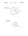
- a dual-stripe current-pinned spin-valve read element 50 includes a dual-stripe current-pinned spin-valve read sensor 52 disposed between the first shield 12 and the second shield 14 , the three of which define an air bearing surface ABS, in an x-y plane 54 , which faces the surface of the magnetic disk (see FIGS. 1A, 1 B) during reading operations.
- the first and second shields 12 and 14 can be separated by a shield-to-shield spacing STS.
- the shield-to-shield spacing STS is measured in the x-direction or downtrack direction.
- the dual-stripe current-pinned spin valve read sensor 52 extends from the ABS in the z-direction, or transverse direction, for a distance termed the stripe height SH. Because two spin valves are included, the read sensor 52 of this embodiment can exhibit a read signal about double that of a single spin valve, thereby significantly enhancing read capability.
- the dual-stripe current-pinned spin valve read sensor 52 includes a first spin valve stripe SV 1 and a second spin valve stripe SV 2 which are separated by an insulation layer INS.
- Each spin valve stripe is formed of two soft ferromagnetic layers separated by a conductive spacer.
- the first spin valve stripe SV 1 includes a first soft ferromagnetic (FM) layer 58 and a second soft ferromagnetic layer 60 , separated from each other by a first spacer 62 .
- the second spin valve stripe SV 2 includes a third soft ferromagnetic layer 64 and a fourth soft ferromagnetic layer 66 which are separated by a second spacer 68 .
- Each of the first, second, third, and fourth FM layers 58 , 60 , 64 , and 66 can be formed of a soft FM material such as permalloy (NiFe), cobalt (Co), cobalt-iron (CoFe), or other soft FM alloy of nickel, iron, and/or cobalt.
- a “soft” ferromagnetic material has low coercivity, e.g., less than 15 oersteds.
- the first and second spacers 62 and 68 can consist essentially of any suitable highly conductive material, such as copper.
- the thicknesses of the layers can be different from each other and are not shown to scale.
- the thicknesses t f1 , t f2 of the second and third soft FM layers 60 , 64 can be in the range of about 40 angstroms to about 100 angstroms.
- the thicknesses t s1 , t s2 of the first and second spacers 62 , 68 can be in the range of about 20 angstroms to about 55 angstroms.
- the thicknesses t p1 , t p2 of the first and fourth soft FM layers 58 , 66 can be in the range of about 10 angstroms to about 55 angstroms.
- a buffer layer also can be included between the second soft FM layer 60 and the first spacer 62 , and between the third soft FM layer 64 and the second spacer 68 .
- buffer layers of CoFe can be disposed between a spacer layer consisting essentially of copper, and a soft FM layer consisting essentially of NiFe.
- the dual-stripe current-pinned spin valve read sensor 52 can additionally incorporate a buffer layer (not shown) which can perform as a seed layer for the formation of the first soft FM layer 58 during fabrication and a capping layer (not shown), similar to those shown in FIG. 3 of the prior art.
- the buffer layer and capping layer can be formed, for example, of tantalum (Ta) or zirconium (Zr).
- the insulation layer INS between the first and second spin valve stripes SV 1 and SV 2 can be formed of any suitable electrically insulating material such as Al 2 O 3 , SiN, or Ta 2 O 5 .
- the thickness of the insulation layer INS is driven by a desire to optimize magnetic coupling between the two spin valve stripes, while maintaining electrical insulation between them.
- the minimum thickness is limited by how thin the fabrication processes can make the insulation layer INS without forming pin holes or without breaking down due to different voltages on either side of the insulation layer INS.
- the insulation layer INS can have a thickness in the range of about 50 angstroms to about 300 angstroms.
- FIG. 7 shows the dual-stripe current-pinned spin-valve read sensor 52 as viewed along the line 7 — 7 of FIG. 6 in the x-y plane, in conjunction with a schematic circuit diagram.
- the stripe dimension referred to as trackwidth TW is indicated in the y-direction, or longitudinal direction.
- a first set of leads, or lead set 72 is shown connected to opposite ends of the first spin valve stripe SV 1 .
- a second set of leads, or lead set 74 is connected to opposite ends of the second spin valve stripe SV 2 .
- These lead sets 72 , 74 include hard bias structures 73 and 75 which abut the opposite ends of the first and second spin valve stripes, respectively, to provide transverse biasing to the spin valves.
- Each set of leads 72 , 74 also facilitates the passing of a separate biasing current to each spin-valve stripe. Therefore, the hard bias structures 73 and 75 can be formed of an electrically conductive, magnetic material, while the remainder of each of the lead sets is formed of a highly conductive material, such as gold or copper. Accordingly, the first set of leads 72 can be used to pass a first biasing current Ib 1 from a first current source CS 1 through the first spin-valve stripe SV 1 , while a second biasing current Ib 2 can be passed from a second current source CS 2 through the second spin valve stripe SV 2 via the second set of leads 74 .
- the first and second sets of leads also connect signal detectors, such as first and second voltage sensors VS 1 , VS 2 , respectively, to the first and second spin valve stripes SV 1 , SV 2 to detect a voltage change across the each spin valve stripe SV 1 , SV 2 .
- the outputs of the first and second voltage sensors VS 1 , VS 2 are combined by a signal manipulator, such as a differential amplifier DA that is connected to the first and second voltage sensors VS 1 , VS 2 .
- the output of the differential amplifier DA is a measure of the difference between the two spin valve signals, which is described below in further detail with respect to FIG. 12 .
- the first and second biasing currents Ib 1 and Ib 2 each can be used to pin a layer of each spin valve stripe, as can be better understood with reference to FIG. 8 .
- FIG. 8 is an enlarged cross-sectional view of the dual-stripe current-pinned spin valve read sensor 52 in the x-z plane. It should be understood that the dimensions shown are not to scale and have been chosen for explanatory purposes only. From this view, magnetic fields due to the biasing currents, here shown flowing out of the viewing plane, can be more easily understood. Because the first and second biasing currents Ib 1 and Ib 2 are in substantially the same direction, the first and second biasing magnetic fields HIb 1 and HIb 2 have substantially the same orientation, here counterclockwise.
- the resulting first biasing magnetic field HIb 1 can saturate the first soft FM layer 58 , thereby pinning its magnetization to form a first pinned layer P 1 .
- an appropriate second biasing current Ib 2 can create a second biasing magnetic field HIb 2 that is sufficiently strong enough to saturate the fourth soft FM layer 66 , to pin its magnetization and form a second pinned layer P 2 .
- the first and second biasing currents Ib 1 and Ib 2 are in substantially the same direction and have substantially the same amplitude. Because no AFM layer is included to provide pinning of the first and second pinned layers P 1 and P 2 , the first and fourth soft ferromagnetic layers are substantially unpinned without the first and second biasing currents.
- the first and second biasing magnetic fields HIb 1 and HIb 2 affect the second and third soft FM layers 60 , 64 in a different way.
- the effects of the two fields upon each of the second and third soft FM layers tend to substantially cancel each other out throughout a majority of each of those two layers.
- the first biasing magnetic field HIb 1 acts from right to left throughout the second soft FM layer 60
- the second biasing magnetic field HIb 2 is from left to right throughout the second soft FM layer.
- the effects in opposite directions substantially cancel each other out.
- a similar effect results in the third soft FM layer 64 .
- the magnetizations of the second and third soft ferromagnetic layers are substantially not affected by the biasing currents, the magnetizations and therefore resistances of those layers are free to be affected by an external magnetic field, such as from a magnetic medium.
- these layers act as first and second free layers F 1 and F 2 in the first and second spin valve stripes, respectively.
- the Mrt product of the first and fourth soft AFM layers 58 , 66 are less than the Mrt products of the second and third soft AFM layers 60 , 64 , respectively.
- each of the soft AFM layers can have an Mrt of about 0.3 to about 0.5 memu/cm 2 .
- the Mrt ratio of the free layer to the pinned layer can be in the range of about 1.1 to about 10.
- the bias currents also must be high enough relative to the Mrt of the respective layer to be pinned.
- the first and fourth soft AFM layers 58 , 66 of the presently described embodiments can be saturated with biasing currents as small as 4 mA.
- FIG. 8A depicts the y-z components of the magnetization directions across the first free layer F 1 .
- the first free layer F 1 magnetization has been set to be substantially longitudinal (i.e., in the y-direction).
- the biasing magnetic fields due to the biasing currents have a negligible effect on the first free layer F 1 magnetization throughout a substantially large portion of the first free layer F 1 .
- the biasing magnetic fields cause the magnetization across the first pinned layer P 1 to align with the biasing magnetic fields, which is substantially orthogonal to the magnetization across the first free layer F 1 as shown in FIG. 8 A.
- the first and second pinned layers P 1 and P 2 are pinned without use of an antiferromagnetic (AFM) layer, the read sensor of the present embodiment is significantly less sensitive to thermal asperities, thus improving the overall read performance capability.
- AFM antiferromagnetic
- FIGS. 10A, 10 B, and 10 C show the magnetizations across the first pinned layer P 1 when exposed to magnetic fields from media transitions with example Mrt's of +0.5, 0, and ⁇ 0.5 memu/cm 2 , respectively.
- FIGS. 10D, 10 E, and 10 F illustrate the magnetizations across the first free layer F 1 with exposure to the same magnetic fields, respectively. In particular, these results were calculated using micromagnetic theoretical simulation. As these figures illustrate, the magnetization of the first pinned layer is substantially unaffected by an impinging external magnetic field (FIGS. 10 A and 10 C).
- the first free layer F 1 reacts to changing external magnetic fields, in a way that changes the resistive response, thereby facilitating data retrieval.
- FIG. 11 shows the transverse, or z-direction, component of the magnetization Mz of each soft FM layer of the dual-stripe current-pinned spin valve sensor 52 , in response to an applied media field.
- the first and second free layers F 1 and F 2 have significant changes in transverse magnetization Mz, while the first and second pinned layers P 1 and P 2 have little to no response to changing external field.
- the first and second free layer F 1 and F 2 data points also indicate an asymmetric response.
- This asymmetry can be quantified by a measure sometimes referred to as the “track average amplitude asymmetry” (TAAA), which is expressed as a percentage.
- TAAA track average amplitude asymmetry
- the asymmetry of each spin valve stripe of the present invention can be further understood with reference to FIG. 12 .
- the read head output of the first and second spin valve stripes SV 1 and SV 2 of FIGS. 7 and 8 is shown for various media Mrt values in FIG. 12 .
- the asymmetry of each individual spin valve stripe is shown by the nature of the dashed curves. The responses are asymmetric, and therefore read performance is less than optimal.
- the dual-stripe current-pinned spin valve read sensor 52 of FIGS. 6-8 has an output which is a measure of the difference in signals from the first and second spin valve stripes SV 1 , SV 2 . This is because the output has been combined with a differential amplifier as shown in FIG. 7 . As can be seen by reference to the solid curve of FIG.
- Such operation of the read sensor is sometimes termed differential mode or common reject mode, and exhibits greater read performance than occurs with either spin valve stripe SV 1 or SV 2 alone.
- Differential mode operation can mitigate the effects of thermal asperities which can change the overall resistance of the device.
- the baseline resistance of the device can be cancelled by taking the difference of the signal from each spin valve.
- the present invention provides structures and methods for providing a magnetoresistive spin valve device that has a larger read signal, has reduced temperature and ESD sensitivity, has increased reliability, and operates in differential mode, and therefore exhibits increased read performance over previous read sensors.
- the invention has been described herein in terms of several preferred embodiments. Other embodiments of the invention, including alternatives, modifications, permutations and equivalents of the embodiments described herein, will be apparent to those skilled in the art from consideration of the specification, study of the drawings, and practice of the invention.
- the above described read sensor can be incorporated with a write element to provide a read/write head, or further incorporated with other components of a disk drive system.
- the embodiments and preferred features described above should be considered exemplary, with the invention being defined by the appended claims, which therefore include all such alternatives, modifications, permutations and equivalents as fall within the true spirit and scope of the present invention.
Abstract
Description
Claims (22)
Priority Applications (2)
| Application Number | Priority Date | Filing Date | Title |
|---|---|---|---|
| US09/247,882 US6801411B1 (en) | 1999-02-10 | 1999-02-10 | Dual stripe spin valve sensor without antiferromagnetic pinning layer |
| JP2000032395A JP2000276720A (en) | 1999-02-10 | 2000-02-09 | Dual stripe spin valve sensor without antiferromagnetic pinning layer |
Applications Claiming Priority (1)
| Application Number | Priority Date | Filing Date | Title |
|---|---|---|---|
| US09/247,882 US6801411B1 (en) | 1999-02-10 | 1999-02-10 | Dual stripe spin valve sensor without antiferromagnetic pinning layer |
Publications (1)
| Publication Number | Publication Date |
|---|---|
| US6801411B1 true US6801411B1 (en) | 2004-10-05 |
Family
ID=22936774
Family Applications (1)
| Application Number | Title | Priority Date | Filing Date |
|---|---|---|---|
| US09/247,882 Expired - Fee Related US6801411B1 (en) | 1999-02-10 | 1999-02-10 | Dual stripe spin valve sensor without antiferromagnetic pinning layer |
Country Status (2)
| Country | Link |
|---|---|
| US (1) | US6801411B1 (en) |
| JP (1) | JP2000276720A (en) |
Cited By (138)
| Publication number | Priority date | Publication date | Assignee | Title |
|---|---|---|---|---|
| US20030214764A1 (en) * | 2002-05-15 | 2003-11-20 | Seagate Technology Llc | V-shape magnetic field sensor with anisotropy induced orthogonal magnetic alignment |
| US20050099740A1 (en) * | 2003-11-12 | 2005-05-12 | Hitachi Global Technologies Netherlands B.V. | Method and apparatus for providing magnetostriction control in a freelayer of a magnetic memory device |
| US20070019340A1 (en) * | 2005-07-22 | 2007-01-25 | Hitachi Global Storage Technologies | Magnetoresistive sensor with in-stack bias layer pinned at the back edge of the sensor stripe |
| US20090015252A1 (en) * | 2007-07-13 | 2009-01-15 | Wolfgang Raberg | Magnetoresistive Magnetic Field Sensor Structure |
| US8830628B1 (en) | 2009-02-23 | 2014-09-09 | Western Digital (Fremont), Llc | Method and system for providing a perpendicular magnetic recording head |
| US8879207B1 (en) | 2011-12-20 | 2014-11-04 | Western Digital (Fremont), Llc | Method for providing a side shield for a magnetic recording transducer using an air bridge |
| US8883017B1 (en) | 2013-03-12 | 2014-11-11 | Western Digital (Fremont), Llc | Method and system for providing a read transducer having seamless interfaces |
| US8917581B1 (en) | 2013-12-18 | 2014-12-23 | Western Digital Technologies, Inc. | Self-anneal process for a near field transducer and chimney in a hard disk drive assembly |
| US8923102B1 (en) | 2013-07-16 | 2014-12-30 | Western Digital (Fremont), Llc | Optical grating coupling for interferometric waveguides in heat assisted magnetic recording heads |
| US8947985B1 (en) | 2013-07-16 | 2015-02-03 | Western Digital (Fremont), Llc | Heat assisted magnetic recording transducers having a recessed pole |
| US8953422B1 (en) | 2014-06-10 | 2015-02-10 | Western Digital (Fremont), Llc | Near field transducer using dielectric waveguide core with fine ridge feature |
| US8958272B1 (en) | 2014-06-10 | 2015-02-17 | Western Digital (Fremont), Llc | Interfering near field transducer for energy assisted magnetic recording |
| US8970988B1 (en) | 2013-12-31 | 2015-03-03 | Western Digital (Fremont), Llc | Electric gaps and method for making electric gaps for multiple sensor arrays |
| US8971160B1 (en) | 2013-12-19 | 2015-03-03 | Western Digital (Fremont), Llc | Near field transducer with high refractive index pin for heat assisted magnetic recording |
| US8976635B1 (en) | 2014-06-10 | 2015-03-10 | Western Digital (Fremont), Llc | Near field transducer driven by a transverse electric waveguide for energy assisted magnetic recording |
| KR20150026913A (en) * | 2013-08-30 | 2015-03-11 | 시게이트 테크놀로지 엘엘씨 | Dual reader structure |
| KR20150026912A (en) * | 2013-08-28 | 2015-03-11 | 시게이트 테크놀로지 엘엘씨 | Dual reader structure |
| US8982508B1 (en) | 2011-10-31 | 2015-03-17 | Western Digital (Fremont), Llc | Method for providing a side shield for a magnetic recording transducer |
| US8980109B1 (en) | 2012-12-11 | 2015-03-17 | Western Digital (Fremont), Llc | Method for providing a magnetic recording transducer using a combined main pole and side shield CMP for a wraparound shield scheme |
| US8988825B1 (en) | 2014-02-28 | 2015-03-24 | Western Digital (Fremont, LLC | Method for fabricating a magnetic writer having half-side shields |
| US8988812B1 (en) | 2013-11-27 | 2015-03-24 | Western Digital (Fremont), Llc | Multi-sensor array configuration for a two-dimensional magnetic recording (TDMR) operation |
| US8984740B1 (en) | 2012-11-30 | 2015-03-24 | Western Digital (Fremont), Llc | Process for providing a magnetic recording transducer having a smooth magnetic seed layer |
| US8995087B1 (en) | 2006-11-29 | 2015-03-31 | Western Digital (Fremont), Llc | Perpendicular magnetic recording write head having a wrap around shield |
| US8993217B1 (en) | 2013-04-04 | 2015-03-31 | Western Digital (Fremont), Llc | Double exposure technique for high resolution disk imaging |
| US9001628B1 (en) | 2013-12-16 | 2015-04-07 | Western Digital (Fremont), Llc | Assistant waveguides for evaluating main waveguide coupling efficiency and diode laser alignment tolerances for hard disk |
| US8997832B1 (en) | 2010-11-23 | 2015-04-07 | Western Digital (Fremont), Llc | Method of fabricating micrometer scale components |
| US9001467B1 (en) | 2014-03-05 | 2015-04-07 | Western Digital (Fremont), Llc | Method for fabricating side shields in a magnetic writer |
| US9007879B1 (en) | 2014-06-10 | 2015-04-14 | Western Digital (Fremont), Llc | Interfering near field transducer having a wide metal bar feature for energy assisted magnetic recording |
| US9007725B1 (en) | 2014-10-07 | 2015-04-14 | Western Digital (Fremont), Llc | Sensor with positive coupling between dual ferromagnetic free layer laminates |
| US9007719B1 (en) | 2013-10-23 | 2015-04-14 | Western Digital (Fremont), Llc | Systems and methods for using double mask techniques to achieve very small features |
| US9013836B1 (en) | 2013-04-02 | 2015-04-21 | Western Digital (Fremont), Llc | Method and system for providing an antiferromagnetically coupled return pole |
| US9042058B1 (en) | 2013-10-17 | 2015-05-26 | Western Digital Technologies, Inc. | Shield designed for middle shields in a multiple sensor array |
| US9042051B2 (en) | 2013-08-15 | 2015-05-26 | Western Digital (Fremont), Llc | Gradient write gap for perpendicular magnetic recording writer |
| US9042057B1 (en) | 2013-01-09 | 2015-05-26 | Western Digital (Fremont), Llc | Methods for providing magnetic storage elements with high magneto-resistance using Heusler alloys |
| US9042208B1 (en) | 2013-03-11 | 2015-05-26 | Western Digital Technologies, Inc. | Disk drive measuring fly height by applying a bias voltage to an electrically insulated write component of a head |
| US9042052B1 (en) | 2014-06-23 | 2015-05-26 | Western Digital (Fremont), Llc | Magnetic writer having a partially shunted coil |
| US9053735B1 (en) | 2014-06-20 | 2015-06-09 | Western Digital (Fremont), Llc | Method for fabricating a magnetic writer using a full-film metal planarization |
| US9064507B1 (en) | 2009-07-31 | 2015-06-23 | Western Digital (Fremont), Llc | Magnetic etch-stop layer for magnetoresistive read heads |
| US9065043B1 (en) | 2012-06-29 | 2015-06-23 | Western Digital (Fremont), Llc | Tunnel magnetoresistance read head with narrow shield-to-shield spacing |
| US9064527B1 (en) | 2013-04-12 | 2015-06-23 | Western Digital (Fremont), Llc | High order tapered waveguide for use in a heat assisted magnetic recording head |
| US9064528B1 (en) | 2013-05-17 | 2015-06-23 | Western Digital Technologies, Inc. | Interferometric waveguide usable in shingled heat assisted magnetic recording in the absence of a near-field transducer |
| US9070381B1 (en) | 2013-04-12 | 2015-06-30 | Western Digital (Fremont), Llc | Magnetic recording read transducer having a laminated free layer |
| US9082423B1 (en) | 2013-12-18 | 2015-07-14 | Western Digital (Fremont), Llc | Magnetic recording write transducer having an improved trailing surface profile |
| US9087527B1 (en) | 2014-10-28 | 2015-07-21 | Western Digital (Fremont), Llc | Apparatus and method for middle shield connection in magnetic recording transducers |
| US9087534B1 (en) | 2011-12-20 | 2015-07-21 | Western Digital (Fremont), Llc | Method and system for providing a read transducer having soft and hard magnetic bias structures |
| US9093639B2 (en) | 2012-02-21 | 2015-07-28 | Western Digital (Fremont), Llc | Methods for manufacturing a magnetoresistive structure utilizing heating and cooling |
| US9104107B1 (en) | 2013-04-03 | 2015-08-11 | Western Digital (Fremont), Llc | DUV photoresist process |
| US9111550B1 (en) | 2014-12-04 | 2015-08-18 | Western Digital (Fremont), Llc | Write transducer having a magnetic buffer layer spaced between a side shield and a write pole by non-magnetic layers |
| US9111564B1 (en) | 2013-04-02 | 2015-08-18 | Western Digital (Fremont), Llc | Magnetic recording writer having a main pole with multiple flare angles |
| US9111558B1 (en) | 2014-03-14 | 2015-08-18 | Western Digital (Fremont), Llc | System and method of diffractive focusing of light in a waveguide |
| US9123358B1 (en) | 2012-06-11 | 2015-09-01 | Western Digital (Fremont), Llc | Conformal high moment side shield seed layer for perpendicular magnetic recording writer |
| US9123362B1 (en) | 2011-03-22 | 2015-09-01 | Western Digital (Fremont), Llc | Methods for assembling an electrically assisted magnetic recording (EAMR) head |
| US9123374B1 (en) | 2015-02-12 | 2015-09-01 | Western Digital (Fremont), Llc | Heat assisted magnetic recording writer having an integrated polarization rotation plate |
| US9123359B1 (en) | 2010-12-22 | 2015-09-01 | Western Digital (Fremont), Llc | Magnetic recording transducer with sputtered antiferromagnetic coupling trilayer between plated ferromagnetic shields and method of fabrication |
| US9135930B1 (en) | 2014-03-06 | 2015-09-15 | Western Digital (Fremont), Llc | Method for fabricating a magnetic write pole using vacuum deposition |
| US9135937B1 (en) | 2014-05-09 | 2015-09-15 | Western Digital (Fremont), Llc | Current modulation on laser diode for energy assisted magnetic recording transducer |
| US9142233B1 (en) | 2014-02-28 | 2015-09-22 | Western Digital (Fremont), Llc | Heat assisted magnetic recording writer having a recessed pole |
| US9147408B1 (en) | 2013-12-19 | 2015-09-29 | Western Digital (Fremont), Llc | Heated AFM layer deposition and cooling process for TMR magnetic recording sensor with high pinning field |
| US9147404B1 (en) | 2015-03-31 | 2015-09-29 | Western Digital (Fremont), Llc | Method and system for providing a read transducer having a dual free layer |
| US9153255B1 (en) | 2014-03-05 | 2015-10-06 | Western Digital (Fremont), Llc | Method for fabricating a magnetic writer having an asymmetric gap and shields |
| US9183854B2 (en) | 2014-02-24 | 2015-11-10 | Western Digital (Fremont), Llc | Method to make interferometric taper waveguide for HAMR light delivery |
| US9190079B1 (en) | 2014-09-22 | 2015-11-17 | Western Digital (Fremont), Llc | Magnetic write pole having engineered radius of curvature and chisel angle profiles |
| US9190085B1 (en) | 2014-03-12 | 2015-11-17 | Western Digital (Fremont), Llc | Waveguide with reflective grating for localized energy intensity |
| US9194692B1 (en) | 2013-12-06 | 2015-11-24 | Western Digital (Fremont), Llc | Systems and methods for using white light interferometry to measure undercut of a bi-layer structure |
| US9202493B1 (en) | 2014-02-28 | 2015-12-01 | Western Digital (Fremont), Llc | Method of making an ultra-sharp tip mode converter for a HAMR head |
| US9202480B2 (en) | 2009-10-14 | 2015-12-01 | Western Digital (Fremont), LLC. | Double patterning hard mask for damascene perpendicular magnetic recording (PMR) writer |
| US9214165B1 (en) | 2014-12-18 | 2015-12-15 | Western Digital (Fremont), Llc | Magnetic writer having a gradient in saturation magnetization of the shields |
| US9214172B2 (en) | 2013-10-23 | 2015-12-15 | Western Digital (Fremont), Llc | Method of manufacturing a magnetic read head |
| US9214169B1 (en) | 2014-06-20 | 2015-12-15 | Western Digital (Fremont), Llc | Magnetic recording read transducer having a laminated free layer |
| US9213322B1 (en) | 2012-08-16 | 2015-12-15 | Western Digital (Fremont), Llc | Methods for providing run to run process control using a dynamic tuner |
| US9230565B1 (en) | 2014-06-24 | 2016-01-05 | Western Digital (Fremont), Llc | Magnetic shield for magnetic recording head |
| US9236560B1 (en) | 2014-12-08 | 2016-01-12 | Western Digital (Fremont), Llc | Spin transfer torque tunneling magnetoresistive device having a laminated free layer with perpendicular magnetic anisotropy |
| US9245545B1 (en) | 2013-04-12 | 2016-01-26 | Wester Digital (Fremont), Llc | Short yoke length coils for magnetic heads in disk drives |
| US9245562B1 (en) | 2015-03-30 | 2016-01-26 | Western Digital (Fremont), Llc | Magnetic recording writer with a composite main pole |
| US9245543B1 (en) | 2010-06-25 | 2016-01-26 | Western Digital (Fremont), Llc | Method for providing an energy assisted magnetic recording head having a laser integrally mounted to the slider |
| US9251813B1 (en) | 2009-04-19 | 2016-02-02 | Western Digital (Fremont), Llc | Method of making a magnetic recording head |
| US9263071B1 (en) | 2015-03-31 | 2016-02-16 | Western Digital (Fremont), Llc | Flat NFT for heat assisted magnetic recording |
| US9263067B1 (en) | 2013-05-29 | 2016-02-16 | Western Digital (Fremont), Llc | Process for making PMR writer with constant side wall angle |
| US9269382B1 (en) | 2012-06-29 | 2016-02-23 | Western Digital (Fremont), Llc | Method and system for providing a read transducer having improved pinning of the pinned layer at higher recording densities |
| US9275657B1 (en) | 2013-08-14 | 2016-03-01 | Western Digital (Fremont), Llc | Process for making PMR writer with non-conformal side gaps |
| US9280990B1 (en) | 2013-12-11 | 2016-03-08 | Western Digital (Fremont), Llc | Method for fabricating a magnetic writer using multiple etches |
| US9286919B1 (en) | 2014-12-17 | 2016-03-15 | Western Digital (Fremont), Llc | Magnetic writer having a dual side gap |
| US9287494B1 (en) | 2013-06-28 | 2016-03-15 | Western Digital (Fremont), Llc | Magnetic tunnel junction (MTJ) with a magnesium oxide tunnel barrier |
| US9305583B1 (en) | 2014-02-18 | 2016-04-05 | Western Digital (Fremont), Llc | Method for fabricating a magnetic writer using multiple etches of damascene materials |
| US9312064B1 (en) | 2015-03-02 | 2016-04-12 | Western Digital (Fremont), Llc | Method to fabricate a magnetic head including ion milling of read gap using dual layer hard mask |
| US9318130B1 (en) | 2013-07-02 | 2016-04-19 | Western Digital (Fremont), Llc | Method to fabricate tunneling magnetic recording heads with extended pinned layer |
| US9336814B1 (en) | 2013-03-12 | 2016-05-10 | Western Digital (Fremont), Llc | Inverse tapered waveguide for use in a heat assisted magnetic recording head |
| US9343087B1 (en) | 2014-12-21 | 2016-05-17 | Western Digital (Fremont), Llc | Method for fabricating a magnetic writer having half shields |
| US9343086B1 (en) | 2013-09-11 | 2016-05-17 | Western Digital (Fremont), Llc | Magnetic recording write transducer having an improved sidewall angle profile |
| US9343098B1 (en) | 2013-08-23 | 2016-05-17 | Western Digital (Fremont), Llc | Method for providing a heat assisted magnetic recording transducer having protective pads |
| US9349394B1 (en) | 2013-10-18 | 2016-05-24 | Western Digital (Fremont), Llc | Method for fabricating a magnetic writer having a gradient side gap |
| US9349392B1 (en) | 2012-05-24 | 2016-05-24 | Western Digital (Fremont), Llc | Methods for improving adhesion on dielectric substrates |
| US9361913B1 (en) | 2013-06-03 | 2016-06-07 | Western Digital (Fremont), Llc | Recording read heads with a multi-layer AFM layer methods and apparatuses |
| US9361914B1 (en) | 2014-06-18 | 2016-06-07 | Western Digital (Fremont), Llc | Magnetic sensor with thin capping layer |
| US9368134B1 (en) | 2010-12-16 | 2016-06-14 | Western Digital (Fremont), Llc | Method and system for providing an antiferromagnetically coupled writer |
| US9384765B1 (en) | 2015-09-24 | 2016-07-05 | Western Digital (Fremont), Llc | Method and system for providing a HAMR writer having improved optical efficiency |
| US9384763B1 (en) | 2015-03-26 | 2016-07-05 | Western Digital (Fremont), Llc | Dual free layer magnetic reader having a rear bias structure including a soft bias layer |
| US9396742B1 (en) | 2012-11-30 | 2016-07-19 | Western Digital (Fremont), Llc | Magnetoresistive sensor for a magnetic storage system read head, and fabrication method thereof |
| US9396743B1 (en) | 2014-02-28 | 2016-07-19 | Western Digital (Fremont), Llc | Systems and methods for controlling soft bias thickness for tunnel magnetoresistance readers |
| US9406331B1 (en) | 2013-06-17 | 2016-08-02 | Western Digital (Fremont), Llc | Method for making ultra-narrow read sensor and read transducer device resulting therefrom |
| US9424866B1 (en) | 2015-09-24 | 2016-08-23 | Western Digital (Fremont), Llc | Heat assisted magnetic recording write apparatus having a dielectric gap |
| US9431031B1 (en) | 2015-03-24 | 2016-08-30 | Western Digital (Fremont), Llc | System and method for magnetic transducers having multiple sensors and AFC shields |
| US9431047B1 (en) | 2013-05-01 | 2016-08-30 | Western Digital (Fremont), Llc | Method for providing an improved AFM reader shield |
| US9431032B1 (en) | 2013-08-14 | 2016-08-30 | Western Digital (Fremont), Llc | Electrical connection arrangement for a multiple sensor array usable in two-dimensional magnetic recording |
| US9431039B1 (en) | 2013-05-21 | 2016-08-30 | Western Digital (Fremont), Llc | Multiple sensor array usable in two-dimensional magnetic recording |
| US9431038B1 (en) | 2015-06-29 | 2016-08-30 | Western Digital (Fremont), Llc | Method for fabricating a magnetic write pole having an improved sidewall angle profile |
| US9437251B1 (en) | 2014-12-22 | 2016-09-06 | Western Digital (Fremont), Llc | Apparatus and method having TDMR reader to reader shunts |
| US9443541B1 (en) | 2015-03-24 | 2016-09-13 | Western Digital (Fremont), Llc | Magnetic writer having a gradient in saturation magnetization of the shields and return pole |
| US9441938B1 (en) | 2013-10-08 | 2016-09-13 | Western Digital (Fremont), Llc | Test structures for measuring near field transducer disc length |
| US9449625B1 (en) | 2014-12-24 | 2016-09-20 | Western Digital (Fremont), Llc | Heat assisted magnetic recording head having a plurality of diffusion barrier layers |
| US9449621B1 (en) | 2015-03-26 | 2016-09-20 | Western Digital (Fremont), Llc | Dual free layer magnetic reader having a rear bias structure having a high aspect ratio |
| US9472216B1 (en) | 2015-09-23 | 2016-10-18 | Western Digital (Fremont), Llc | Differential dual free layer magnetic reader |
| US9484051B1 (en) | 2015-11-09 | 2016-11-01 | The Provost, Fellows, Foundation Scholars and the other members of Board, of the College of the Holy and Undivided Trinity of Queen Elizabeth near Dublin | Method and system for reducing undesirable reflections in a HAMR write apparatus |
| US9508363B1 (en) | 2014-06-17 | 2016-11-29 | Western Digital (Fremont), Llc | Method for fabricating a magnetic write pole having a leading edge bevel |
| US9508365B1 (en) | 2015-06-24 | 2016-11-29 | Western Digital (Fremont), LLC. | Magnetic reader having a crystal decoupling structure |
| US9508372B1 (en) | 2015-06-03 | 2016-11-29 | Western Digital (Fremont), Llc | Shingle magnetic writer having a low sidewall angle pole |
| US9530443B1 (en) | 2015-06-25 | 2016-12-27 | Western Digital (Fremont), Llc | Method for fabricating a magnetic recording device having a high aspect ratio structure |
| US9564150B1 (en) | 2015-11-24 | 2017-02-07 | Western Digital (Fremont), Llc | Magnetic read apparatus having an improved read sensor isolation circuit |
| US9595273B1 (en) | 2015-09-30 | 2017-03-14 | Western Digital (Fremont), Llc | Shingle magnetic writer having nonconformal shields |
| US9646639B2 (en) | 2015-06-26 | 2017-05-09 | Western Digital (Fremont), Llc | Heat assisted magnetic recording writer having integrated polarization rotation waveguides |
| US9666214B1 (en) | 2015-09-23 | 2017-05-30 | Western Digital (Fremont), Llc | Free layer magnetic reader that may have a reduced shield-to-shield spacing |
| US9721595B1 (en) | 2014-12-04 | 2017-08-01 | Western Digital (Fremont), Llc | Method for providing a storage device |
| US9740805B1 (en) | 2015-12-01 | 2017-08-22 | Western Digital (Fremont), Llc | Method and system for detecting hotspots for photolithographically-defined devices |
| US9741366B1 (en) | 2014-12-18 | 2017-08-22 | Western Digital (Fremont), Llc | Method for fabricating a magnetic writer having a gradient in saturation magnetization of the shields |
| US9754611B1 (en) | 2015-11-30 | 2017-09-05 | Western Digital (Fremont), Llc | Magnetic recording write apparatus having a stepped conformal trailing shield |
| US9767831B1 (en) | 2015-12-01 | 2017-09-19 | Western Digital (Fremont), Llc | Magnetic writer having convex trailing surface pole and conformal write gap |
| US9786301B1 (en) | 2014-12-02 | 2017-10-10 | Western Digital (Fremont), Llc | Apparatuses and methods for providing thin shields in a multiple sensor array |
| US9799351B1 (en) | 2015-11-30 | 2017-10-24 | Western Digital (Fremont), Llc | Short yoke length writer having assist coils |
| US9812155B1 (en) | 2015-11-23 | 2017-11-07 | Western Digital (Fremont), Llc | Method and system for fabricating high junction angle read sensors |
| US9842615B1 (en) | 2015-06-26 | 2017-12-12 | Western Digital (Fremont), Llc | Magnetic reader having a nonmagnetic insertion layer for the pinning layer |
| US9858951B1 (en) | 2015-12-01 | 2018-01-02 | Western Digital (Fremont), Llc | Method for providing a multilayer AFM layer in a read sensor |
| US9881638B1 (en) | 2014-12-17 | 2018-01-30 | Western Digital (Fremont), Llc | Method for providing a near-field transducer (NFT) for a heat assisted magnetic recording (HAMR) device |
| US9934811B1 (en) | 2014-03-07 | 2018-04-03 | Western Digital (Fremont), Llc | Methods for controlling stray fields of magnetic features using magneto-elastic anisotropy |
| US9953670B1 (en) | 2015-11-10 | 2018-04-24 | Western Digital (Fremont), Llc | Method and system for providing a HAMR writer including a multi-mode interference device |
| US10037770B1 (en) | 2015-11-12 | 2018-07-31 | Western Digital (Fremont), Llc | Method for providing a magnetic recording write apparatus having a seamless pole |
| US10074387B1 (en) | 2014-12-21 | 2018-09-11 | Western Digital (Fremont), Llc | Method and system for providing a read transducer having symmetric antiferromagnetically coupled shields |
| CN113196078A (en) * | 2019-08-28 | 2021-07-30 | 西部数据技术公司 | Dual free layer TMR magnetic field sensor |
| US11175356B2 (en) * | 2018-12-28 | 2021-11-16 | Tdk Corporation | Magnetic sensor device |
Families Citing this family (3)
| Publication number | Priority date | Publication date | Assignee | Title |
|---|---|---|---|---|
| US6988308B2 (en) * | 2002-01-18 | 2006-01-24 | International Business Machines Corporation | Method of initializing hard bias of a magnetic read head |
| US6801412B2 (en) | 2002-04-19 | 2004-10-05 | International Business Machines Corporation | Method and apparatus for improved pinning strength for self-pinned giant magnetoresistive heads |
| US6781798B2 (en) | 2002-07-15 | 2004-08-24 | International Business Machines Corporation | CPP sensor with dual self-pinned AP pinned layer structures |
Citations (6)
| Publication number | Priority date | Publication date | Assignee | Title |
|---|---|---|---|---|
| US5635835A (en) * | 1994-07-21 | 1997-06-03 | Commissariat A L'energie Atomique | Self biased multilayer magnetoresistance sensor |
| US5796561A (en) * | 1996-11-27 | 1998-08-18 | International Business Machines Corporation | Self-biased spin valve sensor |
| US5856897A (en) * | 1996-11-27 | 1999-01-05 | International Business Machines Corporation | Self-biased dual spin valve sensor |
| US5859753A (en) * | 1996-04-04 | 1999-01-12 | Fujitsu Limited | Spin valve magnetoresistive head with spun valves connected in series |
| US6055136A (en) * | 1995-09-11 | 2000-04-25 | International Business Machines Corporation | Spin valve sensor with antiparallel magnetization of pinned layers |
| US6418000B1 (en) * | 1999-01-21 | 2002-07-09 | Read-Rite Corporation | Dual, synthetic spin valve sensor using current pinning |
-
1999
- 1999-02-10 US US09/247,882 patent/US6801411B1/en not_active Expired - Fee Related
-
2000
- 2000-02-09 JP JP2000032395A patent/JP2000276720A/en active Pending
Patent Citations (6)
| Publication number | Priority date | Publication date | Assignee | Title |
|---|---|---|---|---|
| US5635835A (en) * | 1994-07-21 | 1997-06-03 | Commissariat A L'energie Atomique | Self biased multilayer magnetoresistance sensor |
| US6055136A (en) * | 1995-09-11 | 2000-04-25 | International Business Machines Corporation | Spin valve sensor with antiparallel magnetization of pinned layers |
| US5859753A (en) * | 1996-04-04 | 1999-01-12 | Fujitsu Limited | Spin valve magnetoresistive head with spun valves connected in series |
| US5796561A (en) * | 1996-11-27 | 1998-08-18 | International Business Machines Corporation | Self-biased spin valve sensor |
| US5856897A (en) * | 1996-11-27 | 1999-01-05 | International Business Machines Corporation | Self-biased dual spin valve sensor |
| US6418000B1 (en) * | 1999-01-21 | 2002-07-09 | Read-Rite Corporation | Dual, synthetic spin valve sensor using current pinning |
Cited By (167)
| Publication number | Priority date | Publication date | Assignee | Title |
|---|---|---|---|---|
| US20030214764A1 (en) * | 2002-05-15 | 2003-11-20 | Seagate Technology Llc | V-shape magnetic field sensor with anisotropy induced orthogonal magnetic alignment |
| US7271986B2 (en) * | 2002-05-15 | 2007-09-18 | Seagate Technology Llc | V-shape magnetic field sensor with anisotropy induced orthogonal magnetic alignment |
| US20050099740A1 (en) * | 2003-11-12 | 2005-05-12 | Hitachi Global Technologies Netherlands B.V. | Method and apparatus for providing magnetostriction control in a freelayer of a magnetic memory device |
| US7230802B2 (en) * | 2003-11-12 | 2007-06-12 | Hitachi Global Storage Technologies Netherlands B.V. | Method and apparatus for providing magnetostriction control in a freelayer of a magnetic memory device |
| US20070019340A1 (en) * | 2005-07-22 | 2007-01-25 | Hitachi Global Storage Technologies | Magnetoresistive sensor with in-stack bias layer pinned at the back edge of the sensor stripe |
| US7333305B2 (en) | 2005-07-22 | 2008-02-19 | Hitachi Global Storage Technologies Netherlands B.V. | Magnetoresistive sensor with in-stack bias layer pinned at the back edge of the sensor stripe |
| US8995087B1 (en) | 2006-11-29 | 2015-03-31 | Western Digital (Fremont), Llc | Perpendicular magnetic recording write head having a wrap around shield |
| US20090015252A1 (en) * | 2007-07-13 | 2009-01-15 | Wolfgang Raberg | Magnetoresistive Magnetic Field Sensor Structure |
| DE102007032867B4 (en) * | 2007-07-13 | 2009-12-24 | Infineon Technologies Ag | Magnetoresistive magnetic field sensor structures and manufacturing methods |
| US8063633B2 (en) | 2007-07-13 | 2011-11-22 | Infineon Technologies Ag | Magnetoresistive magnetic field sensor structure |
| DE102007032867A1 (en) * | 2007-07-13 | 2009-01-29 | Infineon Technologies Ag | Magnetoresistive magnetic field sensor structure |
| US8830628B1 (en) | 2009-02-23 | 2014-09-09 | Western Digital (Fremont), Llc | Method and system for providing a perpendicular magnetic recording head |
| US9251813B1 (en) | 2009-04-19 | 2016-02-02 | Western Digital (Fremont), Llc | Method of making a magnetic recording head |
| US9064507B1 (en) | 2009-07-31 | 2015-06-23 | Western Digital (Fremont), Llc | Magnetic etch-stop layer for magnetoresistive read heads |
| US9202480B2 (en) | 2009-10-14 | 2015-12-01 | Western Digital (Fremont), LLC. | Double patterning hard mask for damascene perpendicular magnetic recording (PMR) writer |
| US9245543B1 (en) | 2010-06-25 | 2016-01-26 | Western Digital (Fremont), Llc | Method for providing an energy assisted magnetic recording head having a laser integrally mounted to the slider |
| US9159345B1 (en) | 2010-11-23 | 2015-10-13 | Western Digital (Fremont), Llc | Micrometer scale components |
| US9672847B2 (en) | 2010-11-23 | 2017-06-06 | Western Digital (Fremont), Llc | Micrometer scale components |
| US8997832B1 (en) | 2010-11-23 | 2015-04-07 | Western Digital (Fremont), Llc | Method of fabricating micrometer scale components |
| US9368134B1 (en) | 2010-12-16 | 2016-06-14 | Western Digital (Fremont), Llc | Method and system for providing an antiferromagnetically coupled writer |
| US9123359B1 (en) | 2010-12-22 | 2015-09-01 | Western Digital (Fremont), Llc | Magnetic recording transducer with sputtered antiferromagnetic coupling trilayer between plated ferromagnetic shields and method of fabrication |
| US9123362B1 (en) | 2011-03-22 | 2015-09-01 | Western Digital (Fremont), Llc | Methods for assembling an electrically assisted magnetic recording (EAMR) head |
| US8982508B1 (en) | 2011-10-31 | 2015-03-17 | Western Digital (Fremont), Llc | Method for providing a side shield for a magnetic recording transducer |
| US8879207B1 (en) | 2011-12-20 | 2014-11-04 | Western Digital (Fremont), Llc | Method for providing a side shield for a magnetic recording transducer using an air bridge |
| US9087534B1 (en) | 2011-12-20 | 2015-07-21 | Western Digital (Fremont), Llc | Method and system for providing a read transducer having soft and hard magnetic bias structures |
| US9093639B2 (en) | 2012-02-21 | 2015-07-28 | Western Digital (Fremont), Llc | Methods for manufacturing a magnetoresistive structure utilizing heating and cooling |
| US9349392B1 (en) | 2012-05-24 | 2016-05-24 | Western Digital (Fremont), Llc | Methods for improving adhesion on dielectric substrates |
| US9940950B2 (en) | 2012-05-24 | 2018-04-10 | Western Digital (Fremont), Llc | Methods for improving adhesion on dielectric substrates |
| US9123358B1 (en) | 2012-06-11 | 2015-09-01 | Western Digital (Fremont), Llc | Conformal high moment side shield seed layer for perpendicular magnetic recording writer |
| US9412400B2 (en) | 2012-06-29 | 2016-08-09 | Western Digital (Fremont), Llc | Tunnel magnetoresistance read head with narrow shield-to-shield spacing |
| US9065043B1 (en) | 2012-06-29 | 2015-06-23 | Western Digital (Fremont), Llc | Tunnel magnetoresistance read head with narrow shield-to-shield spacing |
| US9269382B1 (en) | 2012-06-29 | 2016-02-23 | Western Digital (Fremont), Llc | Method and system for providing a read transducer having improved pinning of the pinned layer at higher recording densities |
| US9213322B1 (en) | 2012-08-16 | 2015-12-15 | Western Digital (Fremont), Llc | Methods for providing run to run process control using a dynamic tuner |
| US8984740B1 (en) | 2012-11-30 | 2015-03-24 | Western Digital (Fremont), Llc | Process for providing a magnetic recording transducer having a smooth magnetic seed layer |
| US9396742B1 (en) | 2012-11-30 | 2016-07-19 | Western Digital (Fremont), Llc | Magnetoresistive sensor for a magnetic storage system read head, and fabrication method thereof |
| US8980109B1 (en) | 2012-12-11 | 2015-03-17 | Western Digital (Fremont), Llc | Method for providing a magnetic recording transducer using a combined main pole and side shield CMP for a wraparound shield scheme |
| US9042057B1 (en) | 2013-01-09 | 2015-05-26 | Western Digital (Fremont), Llc | Methods for providing magnetic storage elements with high magneto-resistance using Heusler alloys |
| US9042208B1 (en) | 2013-03-11 | 2015-05-26 | Western Digital Technologies, Inc. | Disk drive measuring fly height by applying a bias voltage to an electrically insulated write component of a head |
| US9336814B1 (en) | 2013-03-12 | 2016-05-10 | Western Digital (Fremont), Llc | Inverse tapered waveguide for use in a heat assisted magnetic recording head |
| US8883017B1 (en) | 2013-03-12 | 2014-11-11 | Western Digital (Fremont), Llc | Method and system for providing a read transducer having seamless interfaces |
| US9111564B1 (en) | 2013-04-02 | 2015-08-18 | Western Digital (Fremont), Llc | Magnetic recording writer having a main pole with multiple flare angles |
| US9013836B1 (en) | 2013-04-02 | 2015-04-21 | Western Digital (Fremont), Llc | Method and system for providing an antiferromagnetically coupled return pole |
| US9104107B1 (en) | 2013-04-03 | 2015-08-11 | Western Digital (Fremont), Llc | DUV photoresist process |
| US8993217B1 (en) | 2013-04-04 | 2015-03-31 | Western Digital (Fremont), Llc | Double exposure technique for high resolution disk imaging |
| US9070381B1 (en) | 2013-04-12 | 2015-06-30 | Western Digital (Fremont), Llc | Magnetic recording read transducer having a laminated free layer |
| US9064527B1 (en) | 2013-04-12 | 2015-06-23 | Western Digital (Fremont), Llc | High order tapered waveguide for use in a heat assisted magnetic recording head |
| US9245545B1 (en) | 2013-04-12 | 2016-01-26 | Wester Digital (Fremont), Llc | Short yoke length coils for magnetic heads in disk drives |
| US9431047B1 (en) | 2013-05-01 | 2016-08-30 | Western Digital (Fremont), Llc | Method for providing an improved AFM reader shield |
| US9064528B1 (en) | 2013-05-17 | 2015-06-23 | Western Digital Technologies, Inc. | Interferometric waveguide usable in shingled heat assisted magnetic recording in the absence of a near-field transducer |
| US9431039B1 (en) | 2013-05-21 | 2016-08-30 | Western Digital (Fremont), Llc | Multiple sensor array usable in two-dimensional magnetic recording |
| US9263067B1 (en) | 2013-05-29 | 2016-02-16 | Western Digital (Fremont), Llc | Process for making PMR writer with constant side wall angle |
| US9361913B1 (en) | 2013-06-03 | 2016-06-07 | Western Digital (Fremont), Llc | Recording read heads with a multi-layer AFM layer methods and apparatuses |
| US9406331B1 (en) | 2013-06-17 | 2016-08-02 | Western Digital (Fremont), Llc | Method for making ultra-narrow read sensor and read transducer device resulting therefrom |
| US9287494B1 (en) | 2013-06-28 | 2016-03-15 | Western Digital (Fremont), Llc | Magnetic tunnel junction (MTJ) with a magnesium oxide tunnel barrier |
| US9318130B1 (en) | 2013-07-02 | 2016-04-19 | Western Digital (Fremont), Llc | Method to fabricate tunneling magnetic recording heads with extended pinned layer |
| US8923102B1 (en) | 2013-07-16 | 2014-12-30 | Western Digital (Fremont), Llc | Optical grating coupling for interferometric waveguides in heat assisted magnetic recording heads |
| US8947985B1 (en) | 2013-07-16 | 2015-02-03 | Western Digital (Fremont), Llc | Heat assisted magnetic recording transducers having a recessed pole |
| US9431032B1 (en) | 2013-08-14 | 2016-08-30 | Western Digital (Fremont), Llc | Electrical connection arrangement for a multiple sensor array usable in two-dimensional magnetic recording |
| US9275657B1 (en) | 2013-08-14 | 2016-03-01 | Western Digital (Fremont), Llc | Process for making PMR writer with non-conformal side gaps |
| US9042051B2 (en) | 2013-08-15 | 2015-05-26 | Western Digital (Fremont), Llc | Gradient write gap for perpendicular magnetic recording writer |
| US9343098B1 (en) | 2013-08-23 | 2016-05-17 | Western Digital (Fremont), Llc | Method for providing a heat assisted magnetic recording transducer having protective pads |
| US9190082B2 (en) | 2013-08-28 | 2015-11-17 | Seagate Technology, Llc | Dual reader structure |
| KR20150026912A (en) * | 2013-08-28 | 2015-03-11 | 시게이트 테크놀로지 엘엘씨 | Dual reader structure |
| US9324342B2 (en) | 2013-08-30 | 2016-04-26 | Seagate Technology Llc | Dual reader structure |
| KR20150026913A (en) * | 2013-08-30 | 2015-03-11 | 시게이트 테크놀로지 엘엘씨 | Dual reader structure |
| US9343086B1 (en) | 2013-09-11 | 2016-05-17 | Western Digital (Fremont), Llc | Magnetic recording write transducer having an improved sidewall angle profile |
| US9441938B1 (en) | 2013-10-08 | 2016-09-13 | Western Digital (Fremont), Llc | Test structures for measuring near field transducer disc length |
| US9042058B1 (en) | 2013-10-17 | 2015-05-26 | Western Digital Technologies, Inc. | Shield designed for middle shields in a multiple sensor array |
| US9349394B1 (en) | 2013-10-18 | 2016-05-24 | Western Digital (Fremont), Llc | Method for fabricating a magnetic writer having a gradient side gap |
| US9007719B1 (en) | 2013-10-23 | 2015-04-14 | Western Digital (Fremont), Llc | Systems and methods for using double mask techniques to achieve very small features |
| US9830936B2 (en) | 2013-10-23 | 2017-11-28 | Western Digital (Fremont), Llc | Magnetic read head with antiferromagentic layer |
| US9214172B2 (en) | 2013-10-23 | 2015-12-15 | Western Digital (Fremont), Llc | Method of manufacturing a magnetic read head |
| US8988812B1 (en) | 2013-11-27 | 2015-03-24 | Western Digital (Fremont), Llc | Multi-sensor array configuration for a two-dimensional magnetic recording (TDMR) operation |
| US9194692B1 (en) | 2013-12-06 | 2015-11-24 | Western Digital (Fremont), Llc | Systems and methods for using white light interferometry to measure undercut of a bi-layer structure |
| US9280990B1 (en) | 2013-12-11 | 2016-03-08 | Western Digital (Fremont), Llc | Method for fabricating a magnetic writer using multiple etches |
| US9001628B1 (en) | 2013-12-16 | 2015-04-07 | Western Digital (Fremont), Llc | Assistant waveguides for evaluating main waveguide coupling efficiency and diode laser alignment tolerances for hard disk |
| US8917581B1 (en) | 2013-12-18 | 2014-12-23 | Western Digital Technologies, Inc. | Self-anneal process for a near field transducer and chimney in a hard disk drive assembly |
| US9082423B1 (en) | 2013-12-18 | 2015-07-14 | Western Digital (Fremont), Llc | Magnetic recording write transducer having an improved trailing surface profile |
| US8971160B1 (en) | 2013-12-19 | 2015-03-03 | Western Digital (Fremont), Llc | Near field transducer with high refractive index pin for heat assisted magnetic recording |
| US9147408B1 (en) | 2013-12-19 | 2015-09-29 | Western Digital (Fremont), Llc | Heated AFM layer deposition and cooling process for TMR magnetic recording sensor with high pinning field |
| US8970988B1 (en) | 2013-12-31 | 2015-03-03 | Western Digital (Fremont), Llc | Electric gaps and method for making electric gaps for multiple sensor arrays |
| US9305583B1 (en) | 2014-02-18 | 2016-04-05 | Western Digital (Fremont), Llc | Method for fabricating a magnetic writer using multiple etches of damascene materials |
| US9183854B2 (en) | 2014-02-24 | 2015-11-10 | Western Digital (Fremont), Llc | Method to make interferometric taper waveguide for HAMR light delivery |
| US9202493B1 (en) | 2014-02-28 | 2015-12-01 | Western Digital (Fremont), Llc | Method of making an ultra-sharp tip mode converter for a HAMR head |
| US9142233B1 (en) | 2014-02-28 | 2015-09-22 | Western Digital (Fremont), Llc | Heat assisted magnetic recording writer having a recessed pole |
| US8988825B1 (en) | 2014-02-28 | 2015-03-24 | Western Digital (Fremont, LLC | Method for fabricating a magnetic writer having half-side shields |
| US9396743B1 (en) | 2014-02-28 | 2016-07-19 | Western Digital (Fremont), Llc | Systems and methods for controlling soft bias thickness for tunnel magnetoresistance readers |
| US9001467B1 (en) | 2014-03-05 | 2015-04-07 | Western Digital (Fremont), Llc | Method for fabricating side shields in a magnetic writer |
| US9349393B2 (en) | 2014-03-05 | 2016-05-24 | Western Digital (Fremont), Llc | Magnetic writer having an asymmetric gap and shields |
| US9153255B1 (en) | 2014-03-05 | 2015-10-06 | Western Digital (Fremont), Llc | Method for fabricating a magnetic writer having an asymmetric gap and shields |
| US9135930B1 (en) | 2014-03-06 | 2015-09-15 | Western Digital (Fremont), Llc | Method for fabricating a magnetic write pole using vacuum deposition |
| US9934811B1 (en) | 2014-03-07 | 2018-04-03 | Western Digital (Fremont), Llc | Methods for controlling stray fields of magnetic features using magneto-elastic anisotropy |
| US9495984B2 (en) | 2014-03-12 | 2016-11-15 | Western Digital (Fremont), Llc | Waveguide with reflective grating for localized energy intensity |
| US9190085B1 (en) | 2014-03-12 | 2015-11-17 | Western Digital (Fremont), Llc | Waveguide with reflective grating for localized energy intensity |
| US9111558B1 (en) | 2014-03-14 | 2015-08-18 | Western Digital (Fremont), Llc | System and method of diffractive focusing of light in a waveguide |
| US9135937B1 (en) | 2014-05-09 | 2015-09-15 | Western Digital (Fremont), Llc | Current modulation on laser diode for energy assisted magnetic recording transducer |
| US9311952B2 (en) | 2014-06-10 | 2016-04-12 | Western Digital (Fremont), Llc | Interfering near field transducer for energy assisted magnetic recording |
| US8953422B1 (en) | 2014-06-10 | 2015-02-10 | Western Digital (Fremont), Llc | Near field transducer using dielectric waveguide core with fine ridge feature |
| US8958272B1 (en) | 2014-06-10 | 2015-02-17 | Western Digital (Fremont), Llc | Interfering near field transducer for energy assisted magnetic recording |
| US9007879B1 (en) | 2014-06-10 | 2015-04-14 | Western Digital (Fremont), Llc | Interfering near field transducer having a wide metal bar feature for energy assisted magnetic recording |
| US8976635B1 (en) | 2014-06-10 | 2015-03-10 | Western Digital (Fremont), Llc | Near field transducer driven by a transverse electric waveguide for energy assisted magnetic recording |
| US9159346B1 (en) | 2014-06-10 | 2015-10-13 | Western Digital (Fremont), Llc | Near field transducer using dielectric waveguide core with fine ridge feature |
| US9508363B1 (en) | 2014-06-17 | 2016-11-29 | Western Digital (Fremont), Llc | Method for fabricating a magnetic write pole having a leading edge bevel |
| US9361914B1 (en) | 2014-06-18 | 2016-06-07 | Western Digital (Fremont), Llc | Magnetic sensor with thin capping layer |
| US9053735B1 (en) | 2014-06-20 | 2015-06-09 | Western Digital (Fremont), Llc | Method for fabricating a magnetic writer using a full-film metal planarization |
| US9214169B1 (en) | 2014-06-20 | 2015-12-15 | Western Digital (Fremont), Llc | Magnetic recording read transducer having a laminated free layer |
| US9042052B1 (en) | 2014-06-23 | 2015-05-26 | Western Digital (Fremont), Llc | Magnetic writer having a partially shunted coil |
| US9230565B1 (en) | 2014-06-24 | 2016-01-05 | Western Digital (Fremont), Llc | Magnetic shield for magnetic recording head |
| US9190079B1 (en) | 2014-09-22 | 2015-11-17 | Western Digital (Fremont), Llc | Magnetic write pole having engineered radius of curvature and chisel angle profiles |
| US9007725B1 (en) | 2014-10-07 | 2015-04-14 | Western Digital (Fremont), Llc | Sensor with positive coupling between dual ferromagnetic free layer laminates |
| US9087527B1 (en) | 2014-10-28 | 2015-07-21 | Western Digital (Fremont), Llc | Apparatus and method for middle shield connection in magnetic recording transducers |
| US9786301B1 (en) | 2014-12-02 | 2017-10-10 | Western Digital (Fremont), Llc | Apparatuses and methods for providing thin shields in a multiple sensor array |
| US10460751B2 (en) | 2014-12-04 | 2019-10-29 | Western Digital (Fremont), Llc | Stripe height lapping control structures for a multiple sensor array |
| US10008222B2 (en) | 2014-12-04 | 2018-06-26 | Western Digital (Fremont), Llc | Stripe height lapping control structures for a multiple sensor array |
| US9721595B1 (en) | 2014-12-04 | 2017-08-01 | Western Digital (Fremont), Llc | Method for providing a storage device |
| US9111550B1 (en) | 2014-12-04 | 2015-08-18 | Western Digital (Fremont), Llc | Write transducer having a magnetic buffer layer spaced between a side shield and a write pole by non-magnetic layers |
| US9705072B2 (en) | 2014-12-08 | 2017-07-11 | Western Digital (Fremont), Llc | Spin transfer torque tunneling magnetoresistive device having a laminated free layer with perpendicular magnetic anisotropy |
| US9236560B1 (en) | 2014-12-08 | 2016-01-12 | Western Digital (Fremont), Llc | Spin transfer torque tunneling magnetoresistive device having a laminated free layer with perpendicular magnetic anisotropy |
| US10553241B2 (en) | 2014-12-17 | 2020-02-04 | Western Digital Technologies, Inc. | Near-field transducer (NFT) for a heat assisted magnetic recording (HAMR) device |
| US9286919B1 (en) | 2014-12-17 | 2016-03-15 | Western Digital (Fremont), Llc | Magnetic writer having a dual side gap |
| US9881638B1 (en) | 2014-12-17 | 2018-01-30 | Western Digital (Fremont), Llc | Method for providing a near-field transducer (NFT) for a heat assisted magnetic recording (HAMR) device |
| US9214165B1 (en) | 2014-12-18 | 2015-12-15 | Western Digital (Fremont), Llc | Magnetic writer having a gradient in saturation magnetization of the shields |
| US9741366B1 (en) | 2014-12-18 | 2017-08-22 | Western Digital (Fremont), Llc | Method for fabricating a magnetic writer having a gradient in saturation magnetization of the shields |
| US10074387B1 (en) | 2014-12-21 | 2018-09-11 | Western Digital (Fremont), Llc | Method and system for providing a read transducer having symmetric antiferromagnetically coupled shields |
| US9343087B1 (en) | 2014-12-21 | 2016-05-17 | Western Digital (Fremont), Llc | Method for fabricating a magnetic writer having half shields |
| US9437251B1 (en) | 2014-12-22 | 2016-09-06 | Western Digital (Fremont), Llc | Apparatus and method having TDMR reader to reader shunts |
| US9449625B1 (en) | 2014-12-24 | 2016-09-20 | Western Digital (Fremont), Llc | Heat assisted magnetic recording head having a plurality of diffusion barrier layers |
| US9123374B1 (en) | 2015-02-12 | 2015-09-01 | Western Digital (Fremont), Llc | Heat assisted magnetic recording writer having an integrated polarization rotation plate |
| US9312064B1 (en) | 2015-03-02 | 2016-04-12 | Western Digital (Fremont), Llc | Method to fabricate a magnetic head including ion milling of read gap using dual layer hard mask |
| US9431031B1 (en) | 2015-03-24 | 2016-08-30 | Western Digital (Fremont), Llc | System and method for magnetic transducers having multiple sensors and AFC shields |
| US9443541B1 (en) | 2015-03-24 | 2016-09-13 | Western Digital (Fremont), Llc | Magnetic writer having a gradient in saturation magnetization of the shields and return pole |
| US9449621B1 (en) | 2015-03-26 | 2016-09-20 | Western Digital (Fremont), Llc | Dual free layer magnetic reader having a rear bias structure having a high aspect ratio |
| US9922672B1 (en) | 2015-03-26 | 2018-03-20 | Western Digital (Fremont), Llc | Dual free layer magnetic reader having a rear bias structure having a high aspect ratio |
| US9384763B1 (en) | 2015-03-26 | 2016-07-05 | Western Digital (Fremont), Llc | Dual free layer magnetic reader having a rear bias structure including a soft bias layer |
| US9245562B1 (en) | 2015-03-30 | 2016-01-26 | Western Digital (Fremont), Llc | Magnetic recording writer with a composite main pole |
| US9147404B1 (en) | 2015-03-31 | 2015-09-29 | Western Digital (Fremont), Llc | Method and system for providing a read transducer having a dual free layer |
| US9263071B1 (en) | 2015-03-31 | 2016-02-16 | Western Digital (Fremont), Llc | Flat NFT for heat assisted magnetic recording |
| US9508372B1 (en) | 2015-06-03 | 2016-11-29 | Western Digital (Fremont), Llc | Shingle magnetic writer having a low sidewall angle pole |
| US9508365B1 (en) | 2015-06-24 | 2016-11-29 | Western Digital (Fremont), LLC. | Magnetic reader having a crystal decoupling structure |
| US9530443B1 (en) | 2015-06-25 | 2016-12-27 | Western Digital (Fremont), Llc | Method for fabricating a magnetic recording device having a high aspect ratio structure |
| US10242700B2 (en) | 2015-06-26 | 2019-03-26 | Western Digital (Fremont), Llc | Magnetic reader having a nonmagnetic insertion layer for the pinning layer |
| US9842615B1 (en) | 2015-06-26 | 2017-12-12 | Western Digital (Fremont), Llc | Magnetic reader having a nonmagnetic insertion layer for the pinning layer |
| US9646639B2 (en) | 2015-06-26 | 2017-05-09 | Western Digital (Fremont), Llc | Heat assisted magnetic recording writer having integrated polarization rotation waveguides |
| US10037773B2 (en) | 2015-06-26 | 2018-07-31 | Western Digital (Fremont), Llc | Heat assisted magnetic recording writer having integrated polarization rotation waveguides |
| US9431038B1 (en) | 2015-06-29 | 2016-08-30 | Western Digital (Fremont), Llc | Method for fabricating a magnetic write pole having an improved sidewall angle profile |
| US10121501B2 (en) | 2015-09-23 | 2018-11-06 | Western Digital (Fremont), Llc | Free layer magnetic reader that may have a reduced shield-to-shield spacing |
| US9666214B1 (en) | 2015-09-23 | 2017-05-30 | Western Digital (Fremont), Llc | Free layer magnetic reader that may have a reduced shield-to-shield spacing |
| US9472216B1 (en) | 2015-09-23 | 2016-10-18 | Western Digital (Fremont), Llc | Differential dual free layer magnetic reader |
| US9424866B1 (en) | 2015-09-24 | 2016-08-23 | Western Digital (Fremont), Llc | Heat assisted magnetic recording write apparatus having a dielectric gap |
| US9384765B1 (en) | 2015-09-24 | 2016-07-05 | Western Digital (Fremont), Llc | Method and system for providing a HAMR writer having improved optical efficiency |
| US9595273B1 (en) | 2015-09-30 | 2017-03-14 | Western Digital (Fremont), Llc | Shingle magnetic writer having nonconformal shields |
| US9484051B1 (en) | 2015-11-09 | 2016-11-01 | The Provost, Fellows, Foundation Scholars and the other members of Board, of the College of the Holy and Undivided Trinity of Queen Elizabeth near Dublin | Method and system for reducing undesirable reflections in a HAMR write apparatus |
| US9953670B1 (en) | 2015-11-10 | 2018-04-24 | Western Digital (Fremont), Llc | Method and system for providing a HAMR writer including a multi-mode interference device |
| US10381029B2 (en) | 2015-11-10 | 2019-08-13 | Western Digital (Fremont), Llc | Method and system for providing a HAMR writer including a multi-mode interference device |
| US10037770B1 (en) | 2015-11-12 | 2018-07-31 | Western Digital (Fremont), Llc | Method for providing a magnetic recording write apparatus having a seamless pole |
| US9812155B1 (en) | 2015-11-23 | 2017-11-07 | Western Digital (Fremont), Llc | Method and system for fabricating high junction angle read sensors |
| US9564150B1 (en) | 2015-11-24 | 2017-02-07 | Western Digital (Fremont), Llc | Magnetic read apparatus having an improved read sensor isolation circuit |
| US9754611B1 (en) | 2015-11-30 | 2017-09-05 | Western Digital (Fremont), Llc | Magnetic recording write apparatus having a stepped conformal trailing shield |
| US9799351B1 (en) | 2015-11-30 | 2017-10-24 | Western Digital (Fremont), Llc | Short yoke length writer having assist coils |
| US10121495B2 (en) | 2015-11-30 | 2018-11-06 | Western Digital (Fremont), Llc | Magnetic recording write apparatus having a stepped conformal trailing shield |
| US9767831B1 (en) | 2015-12-01 | 2017-09-19 | Western Digital (Fremont), Llc | Magnetic writer having convex trailing surface pole and conformal write gap |
| US9997177B2 (en) | 2015-12-01 | 2018-06-12 | Western Digital (Fremont), Llc | Magnetic writer having convex trailing surface pole and conformal write gap |
| US9740805B1 (en) | 2015-12-01 | 2017-08-22 | Western Digital (Fremont), Llc | Method and system for detecting hotspots for photolithographically-defined devices |
| US9858951B1 (en) | 2015-12-01 | 2018-01-02 | Western Digital (Fremont), Llc | Method for providing a multilayer AFM layer in a read sensor |
| US11175356B2 (en) * | 2018-12-28 | 2021-11-16 | Tdk Corporation | Magnetic sensor device |
| US11555870B2 (en) | 2018-12-28 | 2023-01-17 | Tdk Corporation | Magnetic sensor device |
| CN113196078A (en) * | 2019-08-28 | 2021-07-30 | 西部数据技术公司 | Dual free layer TMR magnetic field sensor |
Also Published As
| Publication number | Publication date |
|---|---|
| JP2000276720A (en) | 2000-10-06 |
Similar Documents
| Publication | Publication Date | Title |
|---|---|---|
| US6801411B1 (en) | Dual stripe spin valve sensor without antiferromagnetic pinning layer | |
| US6137662A (en) | Magnetoresistive sensor with pinned SAL | |
| US6108166A (en) | Current-pinned spin valve sensor | |
| US6418000B1 (en) | Dual, synthetic spin valve sensor using current pinning | |
| US6185077B1 (en) | Spin valve sensor with antiferromagnetic and magnetostatically coupled pinning structure | |
| US6185079B1 (en) | Disk drive with thermal asperity reduction circuitry using a magnetic tunnel junction sensor | |
| US6947264B2 (en) | Self-pinned in-stack bias structure for magnetoresistive read heads | |
| JP4841112B2 (en) | MTJ sensor and disk drive system | |
| US6473275B1 (en) | Dual hybrid magnetic tunnel junction/giant magnetoresistive sensor | |
| US6985338B2 (en) | Insulative in-stack hard bias for GMR sensor stabilization | |
| US7505235B2 (en) | Method and apparatus for providing magnetostriction control in a freelayer of a magnetic memory device | |
| US7330339B2 (en) | Structure providing enhanced self-pinning for CPP GMR and tunnel valve heads | |
| US6636389B2 (en) | GMR magnetic transducer with nano-oxide exchange coupled free layers | |
| US20070297102A1 (en) | Method for providing a self-pinned differential gmr sensor and self-pinned differential gmr sensor | |
| CN114730569A (en) | Two-dimensional magnetic recording (TDMR) read head structure with different stack sensors and disk drive incorporating the same | |
| US6456469B1 (en) | Buffer layer of a spin valve structure | |
| US20050002132A1 (en) | Self-pinned in-stack bias structure with improved pinning | |
| US7177120B2 (en) | Self-pinned spin valve sensor with a high coercivity antiparallel (AP) pinned layer | |
| US7204013B2 (en) | Method of manufacturing a magnetoresistive sensor | |
| US7245463B2 (en) | Apparatus for extended self-pinned layer for a current perpendicular to plane head | |
| GB2349735A (en) | Antiparallel (AP) pinned read head with improved GMR | |
| US7171741B2 (en) | Method for extended self-pinned layer for a current perpendicular to plane head | |
| US20150311430A1 (en) | Magnetoresistive sensor | |
| US10249329B1 (en) | Current-perpendicular-to-the-plane (CPP) magnetoresistive (MR) sensor with wedge shaped free layer | |
| US6201672B1 (en) | Spin valve sensor having improved interface between pinning layer and pinned layer structure |
Legal Events
| Date | Code | Title | Description |
|---|---|---|---|
| AS | Assignment |
Owner name: READ-RITE CORPORATION, CALIFORNIA Free format text: ASSIGNMENT OF ASSIGNORS INTEREST;ASSIGNORS:LEDERMAN, MARCOS;GIBBONS, MATTHEW R.;REEL/FRAME:009776/0131 Effective date: 19990204 |
|
| AS | Assignment |
Owner name: TENNENBAUM CAPITAL PARTNERS, LLC, CALIFORNIA Free format text: SECURITY INTEREST;ASSIGNOR:READ-RITE CORPORATION;REEL/FRAME:013616/0399 Effective date: 20021224 |
|
| AS | Assignment |
Owner name: WESTERN DIGITAL (FREMONT), INC., CALIFORNIA Free format text: ASSIGNMENT OF ASSIGNORS INTEREST;ASSIGNOR:READ-RITE CORPORATION;REEL/FRAME:014506/0765 Effective date: 20030731 |
|
| AS | Assignment |
Owner name: READ-RITE CORPORATION, CALIFORNIA Free format text: RELEASE OF SECURITY INTEREST;ASSIGNOR:TENNENBAUM CAPITAL PARTNERS, LLC;REEL/FRAME:014499/0476 Effective date: 20030731 |
|
| AS | Assignment |
Owner name: GENERAL ELECTRIC CAPITAL CORPORATION, AS AGENT, CA Free format text: SECURITY INTEREST;ASSIGNORS:WESTERN DIGITAL TECHNOLOGIES, INC.;WESTERN DIGITAL (FREMONT), INC.;REEL/FRAME:014830/0957 Effective date: 20030919 |
|
| FPAY | Fee payment |
Year of fee payment: 4 |
|
| AS | Assignment |
Owner name: WESTERN DIGITAL TECHNOLOGIES, INC., CALIFORNIA Free format text: RELEASE BY SECURED PARTY;ASSIGNOR:GENERAL ELECTRIC CAPITAL CORPORATION, AS AGENT;REEL/FRAME:020599/0489 Effective date: 20070809 Owner name: WESTERN DIGITAL (FREMONT), INC., CALIFORNIA Free format text: RELEASE BY SECURED PARTY;ASSIGNOR:GENERAL ELECTRIC CAPITAL CORPORATION, AS AGENT;REEL/FRAME:020599/0489 Effective date: 20070809 |
|
| FPAY | Fee payment |
Year of fee payment: 8 |
|
| REMI | Maintenance fee reminder mailed | ||
| AS | Assignment |
Owner name: JPMORGAN CHASE BANK, N.A., AS COLLATERAL AGENT, IL Free format text: SECURITY AGREEMENT;ASSIGNOR:WESTERN DIGITAL (FREMONT), LLC;REEL/FRAME:038710/0845 Effective date: 20160512 Owner name: U.S. BANK NATIONAL ASSOCIATION, AS COLLATERAL AGEN Free format text: SECURITY AGREEMENT;ASSIGNOR:WESTERN DIGITAL (FREMONT), LLC;REEL/FRAME:038744/0675 Effective date: 20160512 Owner name: JPMORGAN CHASE BANK, N.A., AS COLLATERAL AGENT, IL Free format text: SECURITY AGREEMENT;ASSIGNOR:WESTERN DIGITAL (FREMONT), LLC;REEL/FRAME:038744/0755 Effective date: 20160512 |
|
| LAPS | Lapse for failure to pay maintenance fees | ||
| STCH | Information on status: patent discontinuation |
Free format text: PATENT EXPIRED DUE TO NONPAYMENT OF MAINTENANCE FEES UNDER 37 CFR 1.362 |
|
| FP | Lapsed due to failure to pay maintenance fee |
Effective date: 20161005 |
|
| AS | Assignment |
Owner name: WESTERN DIGITAL (FREMONT), LLC, CALIFORNIA Free format text: RELEASE BY SECURED PARTY;ASSIGNOR:U.S. BANK NATIONAL ASSOCIATION, AS COLLATERAL AGENT;REEL/FRAME:045501/0158 Effective date: 20180227 |
|
| AS | Assignment |
Owner name: WESTERN DIGITAL TECHNOLOGIES, INC., CALIFORNIA Free format text: ASSIGNMENT OF ASSIGNORS INTEREST;ASSIGNOR:WESTERN DIGITAL (FREMONT), LLC;REEL/FRAME:050450/0582 Effective date: 20190508 |
|
| AS | Assignment |
Owner name: WESTERN DIGITAL TECHNOLOGIES, INC., CALIFORNIA Free format text: RELEASE OF SECURITY INTEREST AT REEL 038710 FRAME 0845;ASSIGNOR:JPMORGAN CHASE BANK, N.A.;REEL/FRAME:058965/0445 Effective date: 20220203 Owner name: WESTERN DIGITAL (FREMONT), LLC, CALIFORNIA Free format text: RELEASE OF SECURITY INTEREST AT REEL 038710 FRAME 0845;ASSIGNOR:JPMORGAN CHASE BANK, N.A.;REEL/FRAME:058965/0445 Effective date: 20220203 |