US6781451B2 - Switched-capacitor, common-mode feedback circuit for a differential amplifier without tail current - Google Patents
Switched-capacitor, common-mode feedback circuit for a differential amplifier without tail current Download PDFInfo
- Publication number
- US6781451B2 US6781451B2 US10/425,719 US42571903A US6781451B2 US 6781451 B2 US6781451 B2 US 6781451B2 US 42571903 A US42571903 A US 42571903A US 6781451 B2 US6781451 B2 US 6781451B2
- Authority
- US
- United States
- Prior art keywords
- signals
- common
- amplifier
- output
- voltage
- Prior art date
- Legal status (The legal status is an assumption and is not a legal conclusion. Google has not performed a legal analysis and makes no representation as to the accuracy of the status listed.)
- Expired - Fee Related
Links
Images


Classifications
-
- H—ELECTRICITY
- H03—ELECTRONIC CIRCUITRY
- H03F—AMPLIFIERS
- H03F3/00—Amplifiers with only discharge tubes or only semiconductor devices as amplifying elements
- H03F3/45—Differential amplifiers
- H03F3/45071—Differential amplifiers with semiconductor devices only
- H03F3/45479—Differential amplifiers with semiconductor devices only characterised by the way of common mode signal rejection
- H03F3/45632—Differential amplifiers with semiconductor devices only characterised by the way of common mode signal rejection in differential amplifiers with FET transistors as the active amplifying circuit
- H03F3/45636—Differential amplifiers with semiconductor devices only characterised by the way of common mode signal rejection in differential amplifiers with FET transistors as the active amplifying circuit by using feedback means
- H03F3/45641—Measuring at the loading circuit of the differential amplifier
- H03F3/45645—Controlling the input circuit of the differential amplifier
-
- H—ELECTRICITY
- H03—ELECTRONIC CIRCUITRY
- H03F—AMPLIFIERS
- H03F3/00—Amplifiers with only discharge tubes or only semiconductor devices as amplifying elements
- H03F3/005—Amplifiers with only discharge tubes or only semiconductor devices as amplifying elements using switched capacitors, e.g. dynamic amplifiers; using switched capacitors as resistors in differential amplifiers
-
- H—ELECTRICITY
- H03—ELECTRONIC CIRCUITRY
- H03F—AMPLIFIERS
- H03F3/00—Amplifiers with only discharge tubes or only semiconductor devices as amplifying elements
- H03F3/45—Differential amplifiers
- H03F3/45071—Differential amplifiers with semiconductor devices only
- H03F3/45076—Differential amplifiers with semiconductor devices only characterised by the way of implementation of the active amplifying circuit in the differential amplifier
- H03F3/45179—Differential amplifiers with semiconductor devices only characterised by the way of implementation of the active amplifying circuit in the differential amplifier using MOSFET transistors as the active amplifying circuit
- H03F3/45183—Long tailed pairs
- H03F3/45188—Non-folded cascode stages
-
- H—ELECTRICITY
- H03—ELECTRONIC CIRCUITRY
- H03F—AMPLIFIERS
- H03F3/00—Amplifiers with only discharge tubes or only semiconductor devices as amplifying elements
- H03F3/45—Differential amplifiers
- H03F3/45071—Differential amplifiers with semiconductor devices only
- H03F3/45479—Differential amplifiers with semiconductor devices only characterised by the way of common mode signal rejection
- H03F3/45632—Differential amplifiers with semiconductor devices only characterised by the way of common mode signal rejection in differential amplifiers with FET transistors as the active amplifying circuit
- H03F3/45636—Differential amplifiers with semiconductor devices only characterised by the way of common mode signal rejection in differential amplifiers with FET transistors as the active amplifying circuit by using feedback means
- H03F3/45641—Measuring at the loading circuit of the differential amplifier
- H03F3/45654—Controlling the active amplifying circuit of the differential amplifier
-
- H—ELECTRICITY
- H03—ELECTRONIC CIRCUITRY
- H03F—AMPLIFIERS
- H03F2203/00—Indexing scheme relating to amplifiers with only discharge tubes or only semiconductor devices as amplifying elements covered by H03F3/00
- H03F2203/45—Indexing scheme relating to differential amplifiers
- H03F2203/45394—Indexing scheme relating to differential amplifiers the AAC of the dif amp comprising FETs whose sources are not coupled, i.e. the AAC being a pseudo-differential amplifier
-
- H—ELECTRICITY
- H03—ELECTRONIC CIRCUITRY
- H03F—AMPLIFIERS
- H03F2203/00—Indexing scheme relating to amplifiers with only discharge tubes or only semiconductor devices as amplifying elements covered by H03F3/00
- H03F2203/45—Indexing scheme relating to differential amplifiers
- H03F2203/45421—Indexing scheme relating to differential amplifiers the CMCL comprising a switched capacitor addition circuit
-
- H—ELECTRICITY
- H03—ELECTRONIC CIRCUITRY
- H03F—AMPLIFIERS
- H03F2203/00—Indexing scheme relating to amplifiers with only discharge tubes or only semiconductor devices as amplifying elements covered by H03F3/00
- H03F2203/45—Indexing scheme relating to differential amplifiers
- H03F2203/45651—Indexing scheme relating to differential amplifiers the LC comprising two cascode current sources
Definitions
- the present invention generally relates to a circuit for a differential amplifier. More particularly, the present invention relates to a system and method for controlling output-common-mode voltages in differential amplifiers without tail currents.
- CMOS complementary metal oxide
- differential amplifiers include an inverting input and a non-inverting input and corresponding inverting and non-inverting outputs.
- the total current for differential amplifiers is measured by adding the absolute value of the current detected at both the inverting and non-inverting outputs.
- Slew current is defined as the amount of current detected at one amplifier output port when completely tilting one input to the other.
- slew current is used as a measure of an amplifier's efficiency.
- Another important metric is the output swing, which is a measure of how far the amplifier can go from rail to rail before it begins losing gain.
- Common-mode voltage may be created as a result of imbalances in transistor performance and power supply variations. Common-mode voltage may also result from the input source directly or from a previous amplification stage.
- tail current sources are particular types of differential amplifiers as an effective technique for resolving problems associated with common-mode voltages
- tail current sources create inefficiencies and inherently reduce headroom swing in these amplifiers. Therefore, a need exists to be able to derive high output swings from low-power power supplies in CMOS differential amplifiers without tail current sources.
- an embodiment of the invention includes a switched capacitor feedback circuit configured to switch between two or more timing phases of operation.
- the circuit includes (i) a plurality of input ports configured to receive a corresponding plurality of input signals therethrough, and (ii) at least one output port configured to output an adjusting signal.
- the corresponding plurality of input signals includes a number of primary signals and two or more reference signals.
- the adjusting signal is produced based upon a comparison between the number of primary signals and at least one of the reference signals, the comparison occurring during a first of the timing phases.
- the primary signals are adjusted in accordance with the adjusting signal during a second of the timing phases.
- Another embodiment of the invention includes a switched capacitor feedback circuit including (i) a plurality of input ports configured to receive a corresponding plurality of input signals therethrough, and (ii) at least one output port, the output port being configured to output an adjusting signal.
- the corresponding plurality of input signals includes a number of primary signals and two or more reference signals, all of the signals being associated with a first timing phase of operation.
- the adjusting signal is produced based upon a comparison between the number of primary signals and at least one of the reference signals.
- a pair of active devices having gates thereof coupled together, the gates being configured to receive the adjusting signal.
- the active devices are configured to (i) provide a gain to the adjusting signal in accordance with a predetermined gain factor, and (ii) facilitate an adjustment to the number of primary signals based upon the gain during a second timing phase of operation.
- FIG. 1 is a simplified circuit diagram of a conventional folded cascode differential amplifier
- FIG. 2 is a simplified circuit diagram of a conventional telescopic differential amplifier with a tail current source
- FIG. 3 is a simplified circuit diagram of a conventional telescopic differential amplifier without a tail current source
- FIG. 4 depicts a conventional operational amplifier symbol representing the circuit of FIG. 3;
- FIG. 5 depicts the circuit arrangement of FIG. 4 used in a cascode amplifier
- FIG. 6A is an illustration of a conventional switched capacitor circuit arrangement used in a telescopic amplifier without tail current
- FIG. 6B is an illustration of the switched capacitor circuit of FIG. 6A during a first timing phase
- FIG. 6C is an illustration of the switched capacitor circuit of FIG. 6A during a second timing phase
- FIG. 7 is an illustration of a split input transistor technique used in the present invention.
- FIG. 8 is schematic diagram of a circuit constructed and arranged in accordance with an embodiment of the present invention.
- FIG. 9 depicts a switched capacitor circuit configuration used in the embodiment of FIG. 8;
- FIG. 10A is an illustration of exemplary gain factor relationships associated with a first set of split input transistors in the circuit of FIG. 8;
- FIG. 10B is an illustration of exemplary gain factor relationships associated with a second set of split input transistors in the circuit of FIG. 8;
- FIG. 11 illustrates the operation of the switched capacitor circuit and the split transistors in the embodiment of FIG. 8;
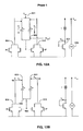
- FIG. 12A depicts a first set of switchable capacitors configured for operation during timing phase 1;
- FIG. 12B depicts a second set of switchable capacitors configured for operation during timing phase 1;
- FIG. 13A depicts the first set of switchable capacitors depicted in FIG. 12A configured for operation during timing phase 2;
- FIG. 13B depicts the second set of switchable capacitors depicted in FIG. 12B configured for operation during timing phase 2.
- FIG. 1 illustrates a conventional folded cascode amplifier 100 , having a maximum non-inverting output current 101 of 2I and a maximum inverting output current 102 , also equal to 2I, for total current output of 4I.
- the folded cascode amplifier 100 has reasonably high total output current, the amplifier 100 is inefficient. Its slew current, described above, is ⁇ I. The slew current is produced by disconnecting one of the amplifier inputs and measuring the amount of current tilting to, or that can be measured at, the other input. Given a total current of 4I, and a slew current of ⁇ I, the amplifier 100 has an efficiency of about 25%.
- the folded cascode amplifier 100 is comparatively slow. That is, any input signal provided at inverting input port IN and non-inverting input port IP must travel around a loop 104 prior to amplification. The signal requires time to completely traverse this loop, thereby creating a slower response time for the amplifier 100 .
- the folded cascode amplifier 100 has a reasonably high output swing of V S ⁇ 4V dsat .
- V S is the supply voltage.
- V dsat is a measure of the source to drain voltage of each of the amplifiers required for each transistor stage to remain in saturation while the amplifier continues to provide full gain.
- FIG. 2 is an illustration of a straight telescopic amplifier 200 .
- the amplifier 200 provides a total non-inverting current output 201 of 2I and a total inverting output current 202 of 2I.
- the total current of the telescopic amplifier 200 is the same as the folded cascode amplifier 100 , 4I, but the slew current is twice as large.
- the telescopic amplifier 200 is faster than the cascode amplifier 100 because it eliminates the signal loop 104 shown in the amplifier 100 .
- the amplifier 200 consumes the same amount of current as the amplifier 104 , but has the advantage of being faster.
- the total output swing of the amplifier 200 is V S ⁇ 6V dsat , lower than that of the output swing of the amplifier 100 .
- the amplifier 100 has an output swing of V s ⁇ 4V dsat
- the amplifier 200 includes a tail current source 208 for controlling common-mode output gain.
- the tail current source 208 is a fixed bias voltage, which helps reject common-mode voltages. Tail currents are undesirable, however, because of the inherent inefficiencies discussed above.
- FIG. 3 shows a telescopic amplifier 300 without a tail current.
- the amplifier 300 provides a total current output of 4I, equal to the total current output of amplifiers 100 and 200 . Further, it does not have the input loop 204 of the amplifier 100 , thus providing an operational speed equivalent to the amplifier 200 . Yet, the amplifier 300 has an output swing of V S ⁇ 4V dSAT , which is greater than the output swing of the amplifier 200 .
- the amplifier 300 offers the features and advantages of the folded cascode amplifier 100 and the straight telescopic amplifier 200 without the need for a tail current. However, without a tail current, the amplifier 300 is unable to reject output to common-mode voltages due to the input source or caused by the previous stage.
- FIG. 4 illustrates a conventional use of differential amplifiers, such as the telescopic amplifier 300 .
- FIG. 4 shows how the telescopic amplifier 300 can be used to form an operational amplifier 400 having respective inverting and non-inverting input ports IN and IP.
- respective inverting and non-inverting differential output ports OP and ON are also included.
- differential amplifiers operate upon the principle that each differential input is sensitive to the opposite polarity of the other. That is, when the non-inverting input receives a positive signal and the inverting input inverts the positive signal to form a negative version thereof, then an output is produced which is equal to a difference between the two signals multiplied by some gain.
- FIG. 5 shows a conventional cascode amplifier 500 including two amplification stages, 502 and 504 .
- the stages 502 and 504 include amplifiers 506 and 508 .
- Each amplifier 506 and 508 has a gain of 4, thus yielding a total gain of 16 for the amplifier 500 . Therefore, in the amplifier 500 , the signal level of desirable signals will be multiplied by a factor of 16 during amplification.
- unwanted signals produced by offsets in the amplification stage 502 will also be multiplied by the factor of 16.
- These amplified unwanted signals i.e., offsets
- these amplifiers often behave as common-mode voltage signals which significantly reduce amplification characteristics, such as dynamic range and head-room of the amplifier 500 . Therefore, although telescopic amplifiers without tail currents inherently reject common-mode voltages, these amplifiers still remain vulnerable to the effects of common-mode type offset voltages.
- Switched capacitor interpolation circuits are routinely used in conjunction with a reference voltage source to further attenuate the effects of output common-mode voltages. As stated above, however, such arrangements are ineffective against offset voltages which may occur as the capacitors of the switched capacitor circuits dump charges from phase to phase transitions, or because of differences in amplification characteristics of the associated transistors. The operation of a conventional telescopic amplifier using a switched capacitor circuit is explained below.
- FIGS. 6A-6C illustrate different operational phases of a conventional telescopic amplifier without tail current, using a switched capacitor circuit.
- FIG. 6A depicts a telescopic amplifier 600 having respective differential non-inverting and inverting amplification sides 602 and 604 .
- the non-inverting amplification side 602 includes a transistor T 1 having a gate acting as an inverting input port IN.
- a non-inverting output port OP also included is a current source I 1 , a capacitor C 1 , and capacitor switches S 1a and S 1b .
- a current source I 2 providing substantially the same level of current as the current source I 1 , is provided, along with a diode D 1 configured to provide a diode voltage.
- the diode D 1 , the current source I 2 , the capacitor C 1 , and the capacitor switches S 1a and S 1b are provided as part of the switched capacitor arrangement discussed above.
- a voltage source V INPUT is included to provide a reference
- the switches S 1a and S 1b are shown to be in a neutral unswitched configuration.
- the non-inverting side 604 includes a transistor T 2 having a gate forming a non-inverting input port IP, an output port ON, and another current source I 1 .
- another diode D 2 is included in the non-inverting side 604 .
- another current source I 2 is included in the non-inverting side 604 .
- another reference voltage source V INPUT is provided.
- the switches S 1a and S 1b are provided to respectively connect terminals of the capacitor C 1 to the diode D 1 and the voltage V INPUT during one timing phase, and to switch the capacitor ends to connect to the gate of the transistor T 1 and the output OP during another timing phase.
- the switches S 2a and S 2b switch the terminals of the capacitor C 2 from being connected to the diode D 2 and the voltage V INPUT during one phase, to having the transistor T 2 and the output ON during the other phase.
- phase 1 and phase 2 As known in the art, traditional switch cap circuits operate through two timing phases (i.e., phase 1 and phase 2). Operation of the telescopic amplifier 600 during phase 1 of the switched capacitor circuit is more clearly illustrated in FIG. 6 B.
- FIG. 6B shows phase 1 of the switched capacitor circuit as mentioned above.
- the switches S 1a and S 1b are configured to provide the voltage V INPUT on one side of the capacitor C 1 while connecting the other side of the capacitor C 1 to the diode D 1 , as shown.
- the diode D 1 which is a field effect transistor (FET) configured as a diode, is provided to mirror the characteristics of transistor T 1 .
- the current source 12 mirrors the current value of the current source I 1 , of the amplification side 602 .
- FET field effect transistor
- the objective of the switch capacitor, the diode D 1 , and the current source I 2 is to attenuate common-mode output voltages provided at the output port OP, limiting these voltages to a value substantially equal to the value V INPUT .
- the capacitor C 1 is connected to have the input voltage source V INPUT at one terminal, and the diode D 1 connected at its other terminal.
- the current source 12 produces a voltage Vgs across a gate of diode D 1 as shown in FIG. 6 B.
- the switches S 2a and S 2b are configured to connect the input voltage V INPUT to one side of C 2 and connect the diode D 2 to its other side, as shown in the figure.
- the characteristics of the diode D 1 and transistor T 1 respectively mirror the characteristics of diode D 2 and transistor T 2 .
- phase 1 when the capacitor C 2 , which is substantially the same value as capacitor C 1 , is connected to and thereby charged with the input voltage V INPUT , the current source 12 of the amplification side 604 also produces the voltage Vgs across a gate of the diode D 2 . Therefore, during phase 1, the capacitor C 1 is charged with a voltage value functionally related to the input voltage V INPUT and the voltage Vgs. Similarly, the capacitor C 2 is charged with a voltage value functionally related to the input voltage V INPUT and the voltage value Vgs, also produced across diode D 2 .
- the switched capacitor circuit switches the capacitor C 1 so that the capacitor C 1 is now inserted (i.e., parked) across the output terminal OP and the input terminal IN of the input side 602 .
- the switches S 2a and S 2b are configured to park the capacitor C 2 across the output ON and the gate of transistor T 2 of the input side 604 .
- FIG. 6C shows phase 2 of the switched capacitor circuit.
- the switches, S 1a and S 1b respectively switch the capacitor C 1 so that it is parked across the output OP and the input IN of the input side 602 .
- the switches S 2a and S 2b switch the capacitor C 2 , so that it is parked across the output ON and the input IP of the input side 604 . Therefore, the voltages that were applied to C 1 during phase 1, V INPUT and Vgs, may now be applied across the output terminal OP and the input terminal IN, respectively.
- the diode voltage Vgs is used as a reference voltage to control the level of the input and output common-mode voltage associated with the input sides 602 and 604 of the amplifier 600 .
- This technique is effective as long as characteristics associated with the diode D 1 carefully match those same characteristics associated with the transistor T 1 . Specifics of this technique will be discussed in detail with regard to the input side 602 only, although it is understood that this technique also applies to the input side 604 .
- the gate characteristics associated with the diode D 1 must carefully match those of the gate of the transistor T 1 , such that when the current source I 2 is used to set up the diode voltage Vgs across the diode gate, substantially the same voltage Vgs is also produced at the gate of the transistor T 1 , which will be a function of the current source I 1 . Therefore, when the capacitor C 1 switches from phase 1 to phase 2 and imparts Vgs across the gate of the transistor T 1 and V INPUT across the terminal OP, the output common-mode voltage is held to the value of V INPUT .
- the output common-mode voltage can be attenuated and held to the voltage level V INPUT as long as the characteristics of the diode D 1 gate match those of the gate of transistor T 1 . If this relationship holds true, then when the capacitor C 1 changes from phase 1 to phase 2, the diode voltage Vgs will be the same at the diode gate and the transistor gate.
- Switched capacitor techniques are effective for reducing common-mode voltages when the characteristics of the amplifier's transistors are carefully matched. This technique, however, is not effective when imbalances, offsets, and/or differences in gate characteristics between the diode and the transistor gate exist. In other words, the technique illustrated in FIGS. 6A-6C is only effective at attenuating common-mode voltage in telescopic amplifiers without tail current. Therefore, an improved technique is needed.
- amplifiers without tail currents may be provided with techniques that not only attenuate common-mode voltages, but also compensate for the effects of common-mode offsets.
- FIG. 7 illustrates that any traditional amplifier without a tail current, such as the telescopic amplifier 300 shown in FIG. 3, can be modified to compensate for the effects of common-mode offsets.
- a first step in this modification requires that the amplifiers' input stage transistors, 700 and 702 , be divided into transistor pairs 704 and 706 respectively.
- the transistor 700 is split into transistors 700 a and 700 b . That is, the gain characteristics associated with the single transistor 700 are divided between the two transistors 700 a and 700 b of the transistor pair 704 . Further, the gain characteristics of transistor 702 are divided between the transistors 702 a and 702 b of the transistor pair 706 .
- FIG. 8 illustrates an exemplary implementation of the split transistor technique shown in FIG. 7 .
- an exemplary amplifier 800 is constructed and arranged in accordance with a preferred embodiment of the present invention.
- the amplifier 800 is a modified telescopic differential amplifier although the present invention may be used with any differential amplifier that does not have a tail current.
- the transistors are metal oxide semiconductor field-effect transistor (MOSFET) devices of the N-channel (NMOS) variety. The present invention, however, is not limited to NMOS transistors.
- the amplifier 800 includes respective first and second amplification sides 801 and 802 .
- the amplification side 801 includes an amplifier inverting input stage 804 having a signal input transistor 805 with its gate forming an input labeled “IN” and a companion transistor 806 .
- transistors 808 - 810 representing individual amplification stages.
- a non-inverting output labeled “OP” is provided to output a differential signal.
- the input side 802 includes anon-inverting amplifier input stage 812 having an input transistor 814 with its gate forming a non-inverting input terminal labeled “IP” along with a companion transistor 815 . Gates g n and g p of the respective companion transistors 806 and 815 , are connected together. Also included in the input side 802 are input stage transistors 818 - 820 .
- the amplifier 800 includes a first voltage source 822 for providing a reference voltage V b4r , a current source 824 providing a current I 1 , a second voltage source 826 for providing a signal representative of a desired fixed common-mode voltage level V cm , and a supply voltage source V S . Common nodes 828 and 829 are provided to electrically connect the input sides 801 and 802 and their associated components.
- the input stages 804 and 812 are constructed of differential pair transistors respectively formed from transistor pairs 805 , 806 and 814 , 815 .
- the differential pair transistors 805 , 806 and 814 , 815 maybe formed by splitting input stage transistors, such as the transistors 700 and 702 shown in FIG. 7 . The idea is to divide the gain characteristics of the single transistor, in a conventional differential amplifier, across the transistor pair.
- the sources of transistors 805 , 806 , 814 and 815 are all connected to a common node 829 of the amplifier 800 .
- one end of the voltage source 826 and an anode side of the diode voltage source 822 are also connected to the common node 829 .
- the gates g n and g p of transistors 806 and 815 are coupled to the connecting line L 1 and are both structured to receive an adjusting voltage signal V b4 .
- drains of the transistors 805 and 806 are connected together and are coupled to the source of transistor 810 .
- the drains of transistors 814 and 815 are connected together and are coupled with the source of transistor 820 .
- the supply voltage V S is provided to the common node 828 to provide an operational voltage to the amplifier 800 .
- the amplifier 800 includes a common-mode feedback circuit 830 , provided in cooperative arrangement with the outputs OP and ON and the input stages 804 and 812 .
- the common-mode feedback circuit 830 cooperates with the amplifier input stages 804 and 812 and provides a feedback loop to attenuate the effects of common-mode offset voltages produced at the outputs OP and ON.
- the feedback circuit 830 includes input ports 833 and 834 for respectively receiving signals produced at the output ports OP and ON. Also included are input ports 831 and 832 for receiving respective voltage signals V cm and V b4r .
- an output port 836 provides the adjusting voltage Vb 4 along the output line L 1 .
- the voltage V b4 is injected into the gates g n and g p of the respective transistors 806 and 815 . More specifically, the common-mode feedback circuit 830 monitors the actual output common-mode voltage provided at the outputs OP and ON. The circuit 830 then compares the actual common-mode voltage occurring at OP and ON with the fixed desirable voltage V cm and correspondingly adjusts the common-mode output voltage, using V b4 to change the output common-mode voltage to the desirable voltage level.
- the common-mode feedback circuit 830 is known in the art as a switched capacitor circuit.
- the common-mode feedback circuit 830 includes two sets of capacitors that are alternately switched between the various input and output ports shown in FIG. 8 .
- the input stages 804 and 812 are configured to adjust an input common-mode voltage based upon an output from the common-mode feedback circuit 830 in a predetermined manner.
- the common-mode feedback circuit 830 is described more fully with reference to the illustration of FIG. 9 .
- the operation of the input stages 804 and 812 will be described more fully in reference to the illustrations shown in FIGS. 10A and 10B.
- FIG. 9 is a schematic diagram of the switchable capacitors included in the common-mode feedback circuit 830 .
- the switched capacitor circuit 830 includes respective first and second capacitor sets 902 and 904 .
- the capacitor sets 902 and 904 are switched between the various amplifier inputs and outputs in a ping-pong like fashion. In this manner, at least one set of capacitors always remains connected across the amplifier inputs and outputs to avoid the creation of an open loop circuit condition.
- the first set of capacitors 902 includes respective first and second capacitors C 1a and C 2b and associated switches S 1 -S 3 for switching the capacitors C 1a and C 2a between first and second timing phases.
- the capacitors C 1a and C 2a are switched from being connected to the output ports OP, V b4 , and ON during a first timing phase of operation, to being connected to V cm and V b4 during a second timing phase.
- the second set of capacitors 904 includes individual capacitors C 1b and C 2b as well as switches S 4 -S 6 for alternately connecting the capacitors C 1b and C 2b between the first and second timing phases discussed above.
- the capacitors C 1b and C 2b are switched from the output ports V cm and V b4r during phase 1, to the outputs OP, V b4 , and ON, during phase 2.
- FIGS. 10A and 10B provide simplified illustrations of the input stages 804 and 812 depicted in FIG. 8 .
- FIGS. 10A and 10B illustrate how transistor input amplification characteristics are divided between respective input transistors 805 and 814 of the input stage 804 and 812 and the respective companion transistors 806 and 815 .
- the gates g n and g p of the companion transistors 806 and 815 are coupled to the output port 836 of the common-mode feedback circuit 830 .
- the companion transistors 806 and 815 are configured to receive the adjustment voltage V b4 , produced by the common-mode feedback circuit 830 along the output line L 1 . Having received the adjusting voltage V b4 the companion transistor 806 and 815 may then adjust the common-mode voltage level, measured at the output ports OP and ON, by some predetermined amount.
- a characteristic unique to common-mode voltage signals is that they have the same polarity on both the input and output sides of amplifiers. On this basis, unwanted common-mode voltage signals can be distinguished from useful differential-mode voltage signals and can therefore be separately processed by the amplifier. That is, differential-mode voltage signals are not attenuated in the exemplary embodiment of FIG. 8 . Only common-mode voltage signals are effected.
- the input stage transistors 805 and 814 are configured to amplify a common-mode input signal in accordance with a predetermined gain, for example driving its signal level from a first value to a second higher value.
- the companion transistors 806 and 815 based upon the output from the common-mode feedback circuit 830 , will drive the signal level to a lower value by the predetermined amount discussed above.
- the common-mode feedback circuit 830 and the input stages 804 and 812 form a feedback path to sample the output common-mode voltage from OP and ON, compare the sampled voltage with the voltage V cm and produce the adjusting signal V b4 as a result.
- the companion transistors 806 and 815 receive this adjusting voltage signal and adjust the voltage level of the output common-mode signal by the predetermined set amount. This process, explained in greater detail below, carefully controls the output common-mode voltage.
- the present invention is thus configured to lower the output common-mode voltage level when the common-mode output voltage is too high, as compared to the desirable reference voltage V cm .
- the present invention is also configured to raise the output common-mode voltage level when the output common-mode voltage is lower than V cm .
- the transistor pairs 805 / 814 and 806 / 815 are structured to provide complimentary gain values in order to process the input and output differential and common-mode voltage signals.
- the transistor pairs 805 / 814 and 806 / 815 thus operate in accordance with respective gain factors 1002 and 1004 .
- gain factors 1002 and 1004 For purposes of illustration only, 3 ⁇ 4 ⁇ and 1 ⁇ 4 ⁇ have been respectively chosen for the factors 1002 and 1004 . It should be understood, however, that any factors may be chosen as long as their sum is substantially equal to one (e.g., 2 ⁇ 5 & 3 ⁇ 5, 1 ⁇ 2 & 1 ⁇ 2, and 1 ⁇ 3 & 2 ⁇ 3 etc.).
- the gain factor 1002 and the corresponding transistors 805 and 814 are used to provide amplification for the useful differential-mode signals received at the input ports IN and IP respectively.
- the gain factor 1004 and the associated transistors 806 and 815 are used to compliment the operation of transistors 805 and 814 and to adjust the output common-mode voltage.
- the transistors 806 and 815 are used to either attenuate or amplify the common-mode voltage provided to the output ports OP and ON, based upon a comparison with the fixed level voltage signal V cm . This principle is illustrated more clearly in the example of FIG. 11 .
- FIG. 11 explains the operation of the present invention.
- output signals are delivered to the output ports OP and ON of the amplifier 800 , they are also respectively provided as inputs to the input ports 833 and 834 of the common-mode feedback circuit 830 .
- an actual common-mode voltage level of these signals is measured and compared with the desirable common-mode voltage signal V cm supplied by the voltage source 826 .
- the capacitors C 1a and C 2a hold an amount of charge acquired during a previous phase, based on the voltage V cm .
- the common-mode feedback circuit 830 reacts to adjust the output common-mode voltage level. Specifically, if the common-mode voltage at the input port 833 and 834 is too high, the common-mode feedback circuit 830 produces a correcting signal S C .
- S C has the voltage level of V b4 and is produced to provide the needed adjustment to the common-mode output voltage level.
- the correcting signal S C is injected into the gates g n and g p of the transistors 806 and 815 .
- the transistors 806 and 814 behave as inverting amplifiers. Therefore, in response to the gates g n and g p going up, during phase 2, the common-mode voltage produced at the outputs OP and ON, is correspondingly drawn down, as represented by the arrows a P2 . Thus, whenever the output common-mode voltage at the output ports OP and ON is higher than V cm during one phase, the common-mode feedback circuit 830 and the transistors 806 and 815 cooperate to reduce the common-mode voltage during the next phase.
- the common-mode feedback circuit 830 and the transistors 806 and 815 cooperate to increase the output common-mode voltage in association with the gain factor 1004 .
- input signals received at the input ports IN and IP are amplified based upon the gain factor 1002 .
- the input differential-mode signals will be amplified by a nominal gain moderated by the factor 3 ⁇ 4 ⁇ .
- the present invention therefore, provides a feedback loop operating between phase 1 and phase 2 of the switch capacitor circuitry to dynamically adjust the output common-mode voltage. In this manner, the effects of common-mode type voltage offsets can be minimized.
- FIGS. 12A-13B provide a more detailed illustration of the operation of the common-mode feedback circuit 830 and the input stages 804 and 812 .
- the switch capacitor circuits are configured to operate during timing phases 1 and 2. As shown in FIG. 9 the capacitors C 1a , C 2a , C 1b , and C 2b , and the switches S 1 -S 6 , are ping-ponged in and out of the common-mode feedback circuit 830 in accordance with the phases 1 and 2.
- the capacitors C 1b and C 2b are configured for connection between the input ports 831 and 832 .
- the desirable voltage V cm is injected into the common-mode feedback circuit 830 through the input port 831 .
- the reference voltage V b4r is injected in to the common-mode feedback circuit 830 through the input port 832 .
- the reference voltage V b4r is generated by the diode voltage source 822 and is provided as the proper reference voltage level needed to precisely adjust the actual output common-mode voltage to match the desired voltage level V cm .
- the capacitors C 1b and C 2b sample, or are charged in accordance with, a voltage V X , which is a function of the voltages V cm and V b4r as measured across capacitors C 1b and C 2b .
- the capacitors C 1a and C 2a are configured as shown in FIG. 12 B. That is, capacitor C 1a is connected between the output port OP and the correcting voltage source V b4 , while the capacitor C 2a is connected between the output port ON and the correcting voltage V b4 .
- the capacitors C 1a and C 2a cooperate to compare the actual common-mode voltage, defined as (V A +V B )/2, with the voltage V X .
- the voltage V X is substantially equal to the desired common-mode voltage V cm . This process occurs as the capacitors C 1a and C 2a discharge across the terminals OP and ON.
- the capacitors C 1a and C 2a correspondingly pull the value of V b4 up or down, based upon the difference between (V A +V B )/2 and V X .
- the adjusting voltage V b4 is then injected into the gates g n and g p of the transistors 806 and 815 respectively.
- the gain factor 1004 is then applied to V b4 and in-turn reflected in the common-mode output voltage during the ensuing phase.
- the present invention provides at least two sets of capacitors, insuring that at least one set is parked across the amplifier at any given point in time. While one set of capacitors compares the desired common-mode voltage signal V cm with the reference voltage signal V b4r and charges the capacitors accordingly, another set of capacitors samples the actual output common-mode voltage (V A +V B )/2 and produces a correcting voltage V b4 . While one set of capacitors is sampling and comparing the other set of capacitors is discharging and correcting.
- the capacitors C 1b and C 2b respectively sample the desirable common-mode output voltage signal V cm and the reference voltage signal V b4r .
- the capacitors C 1b and C 2b previously connected between V cm and V b4r , are switched to respectively connect across the outputs OP and ON and the adjusting voltage V b4 . That is during phase 1 capacitors C 1b and C 2b were charged by voltage V X , a function of V cm and V b4r .
- the capacitors C 1b and C 2b discharge and inject the adjusting voltage V b4 into the gates g n and g p of the respective transistors 806 and 815 . Therefore, using capacitors C 1b and C 2b as an example, during phase 1 the capacitors are loaded with the correct common-mode voltage level having V cm on one side, and the reference voltage V b4r on the other side.
- the capacitors discharge the adjusting voltage V b4 and inject V b4 into the gates g n and g p of the transistors 806 and 815 .
- the parasitic capacitance values of these gates are adjusted in accordance with the gain adjustment factor 1004 shown in FIG. 11 .
- the output common-mode voltage levels are then correspondingly pulled down, or up, in accordance with this value.
- the desirable voltage level signal V cm is again compared with the actual output common-mode voltage (V A +V B )/2 as seen at the output terminals OP and ON. If, for example, the actual common-mode voltage is equal to V cm and the reference voltage V b4r is equal to the correcting voltage V b4 , then no adjustment will be made. If, however, the actual output common-mode voltage is higher than V cm , then the fixed voltage V X across the capacitors C 1b and C 2b will then pull the middle node V b4 , correspondingly higher.
- the fixed voltage V X is analogous to placing a battery between each of the terminals 833 and 834 and the output node 836 . Therefore; the fixed voltage, behaving as a battery, will also pull the correcting voltage V b4 correspondingly higher, which will in turn pull the output common-mode voltage of the amplifier correspondingly lower, since the transistors 806 and 815 act as inverting amplifiers.
- the capacitors C 1b and C 2b are ping-ponged between the common-mode feedback circuit 830 in accordance with phase 1 and phase 2.
- the aforementioned process switches between the capacitors C 1b and C 2b and the capacitors C 1a and C 2a during the respective phases.
- the capacitors C 1a and C 2a are sampling and comparing the actual common-mode voltage, as seen on the output terminals OP and ON, with the desirable common-mode voltage V cm .
- the present invention provides an accurate and reliable circuit and method to dynamically sample the common-mode output voltage of an amplifier without tail current compare this output common-mode voltage with a reference signal and adjust the common-mode input voltage in a manner to dynamically adjust the output common-mode voltage to the desirable level.
- This circuit arrangement and technique therefore creates the ability to compensate for the effects of common-mode type offset voltages caused by variations in electrical characteristics associated with amplifier transistors.
- the circuit arrangement rejects input common-mode voltages created by the input source or by a previous amplification stage.
Abstract
Description
Claims (11)
Priority Applications (2)
| Application Number | Priority Date | Filing Date | Title |
|---|---|---|---|
| US10/425,719 US6781451B2 (en) | 2000-08-03 | 2003-04-30 | Switched-capacitor, common-mode feedback circuit for a differential amplifier without tail current |
| US10/918,550 US6930545B2 (en) | 2000-08-03 | 2004-08-16 | Switched-capacitor, common-mode feedback circuit for a differential amplifier without tail current |
Applications Claiming Priority (4)
| Application Number | Priority Date | Filing Date | Title |
|---|---|---|---|
| US22328000P | 2000-08-03 | 2000-08-03 | |
| US22416800P | 2000-08-09 | 2000-08-09 | |
| US09/921,000 US6577184B2 (en) | 2000-08-03 | 2001-08-03 | Switched-capacitor, common-mode feedback circuit for a differential amplifier without tail current |
| US10/425,719 US6781451B2 (en) | 2000-08-03 | 2003-04-30 | Switched-capacitor, common-mode feedback circuit for a differential amplifier without tail current |
Related Parent Applications (1)
| Application Number | Title | Priority Date | Filing Date |
|---|---|---|---|
| US09/921,000 Continuation US6577184B2 (en) | 2000-08-03 | 2001-08-03 | Switched-capacitor, common-mode feedback circuit for a differential amplifier without tail current |
Related Child Applications (1)
| Application Number | Title | Priority Date | Filing Date |
|---|---|---|---|
| US10/918,550 Continuation US6930545B2 (en) | 2000-08-03 | 2004-08-16 | Switched-capacitor, common-mode feedback circuit for a differential amplifier without tail current |
Publications (2)
| Publication Number | Publication Date |
|---|---|
| US20030201825A1 US20030201825A1 (en) | 2003-10-30 |
| US6781451B2 true US6781451B2 (en) | 2004-08-24 |
Family
ID=26917619
Family Applications (3)
| Application Number | Title | Priority Date | Filing Date |
|---|---|---|---|
| US09/921,000 Expired - Lifetime US6577184B2 (en) | 2000-08-03 | 2001-08-03 | Switched-capacitor, common-mode feedback circuit for a differential amplifier without tail current |
| US10/425,719 Expired - Fee Related US6781451B2 (en) | 2000-08-03 | 2003-04-30 | Switched-capacitor, common-mode feedback circuit for a differential amplifier without tail current |
| US10/918,550 Expired - Fee Related US6930545B2 (en) | 2000-08-03 | 2004-08-16 | Switched-capacitor, common-mode feedback circuit for a differential amplifier without tail current |
Family Applications Before (1)
| Application Number | Title | Priority Date | Filing Date |
|---|---|---|---|
| US09/921,000 Expired - Lifetime US6577184B2 (en) | 2000-08-03 | 2001-08-03 | Switched-capacitor, common-mode feedback circuit for a differential amplifier without tail current |
Family Applications After (1)
| Application Number | Title | Priority Date | Filing Date |
|---|---|---|---|
| US10/918,550 Expired - Fee Related US6930545B2 (en) | 2000-08-03 | 2004-08-16 | Switched-capacitor, common-mode feedback circuit for a differential amplifier without tail current |
Country Status (5)
| Country | Link |
|---|---|
| US (3) | US6577184B2 (en) |
| EP (1) | EP1380101B1 (en) |
| AT (1) | ATE466402T1 (en) |
| DE (1) | DE60141984D1 (en) |
| WO (1) | WO2002013377A2 (en) |
Cited By (5)
| Publication number | Priority date | Publication date | Assignee | Title |
|---|---|---|---|---|
| US7109797B1 (en) * | 2003-10-28 | 2006-09-19 | Analog Devices, Inc. | Method and apparatus for measuring the common-mode component of a differential signal |
| US20070040607A1 (en) * | 2005-08-19 | 2007-02-22 | Micron Technology, Inc. | Switched capacitor amplifier with higher gain and improved closed-loop gain accuracy |
| US20090058526A1 (en) * | 2007-09-04 | 2009-03-05 | International Business Machines Corporation | Common mode feedback amplifier with switched differential capacitor |
| US7560987B1 (en) * | 2005-06-07 | 2009-07-14 | Cypress Semiconductor Corporation | Amplifier circuit with bias stage for controlling a common mode output voltage of the gain stage during device power-up |
| US20100148868A1 (en) * | 2008-12-15 | 2010-06-17 | Nec Electronics Corporation | Differential amplifier |
Families Citing this family (22)
| Publication number | Priority date | Publication date | Assignee | Title |
|---|---|---|---|---|
| DE10249835B4 (en) * | 2002-10-25 | 2008-04-03 | Infineon Technologies Ag | Fully differential operational amplifier |
| US6937100B2 (en) * | 2003-12-18 | 2005-08-30 | Standard Microsystems Corporation | Amplifier circuit with common mode feedback |
| US7012463B2 (en) * | 2003-12-23 | 2006-03-14 | Analog Devices, Inc. | Switched capacitor circuit with reduced common-mode variations |
| US7053712B2 (en) * | 2004-07-30 | 2006-05-30 | International Business Machines Corporation | Method and apparatus for controlling common-mode output voltage in fully differential amplifiers |
| DE602005006704D1 (en) * | 2004-11-08 | 2008-06-26 | Fujifilm Corp | Use of an agent for the removal of oxygen |
| US7233202B2 (en) * | 2005-03-14 | 2007-06-19 | Realtek Semiconductor Corp. | Amplifier with increased bandwidth and method thereof |
| US7138865B1 (en) | 2005-10-04 | 2006-11-21 | Analog Devices, Inc. | Differential amplifiers with enhanced gain and controlled common-mode output level |
| US7629848B2 (en) * | 2006-07-07 | 2009-12-08 | Broadcom Corporation | Operational amplifier with extended common-mode input range |
| EP1901425B1 (en) * | 2006-09-12 | 2018-08-08 | Realtek Semiconductor Corp. | Amplifier with increased bandwidth and method thereof |
| US20090104873A1 (en) * | 2007-10-18 | 2009-04-23 | Broadcom Corporation | Fully integrated compact cross-coupled low noise amplifier |
| JP2009284050A (en) * | 2008-05-20 | 2009-12-03 | Nec Electronics Corp | Differential amplifier circuit |
| US7746171B2 (en) * | 2008-07-25 | 2010-06-29 | Analog Devices, Inc. | Amplifier networks with controlled common-mode level and converter systems for use therewith |
| US20130015918A1 (en) * | 2011-07-15 | 2013-01-17 | Texas Instruments Incorporated | High speed amplifier |
| US8576007B2 (en) | 2011-09-09 | 2013-11-05 | Texas Instruments Incorporated | High speed amplifier |
| KR20130069147A (en) * | 2011-12-16 | 2013-06-26 | 삼성전자주식회사 | Apparatus and circuit for amplifying baseband signal |
| US8570095B1 (en) * | 2012-05-11 | 2013-10-29 | Semiconductor Components Industries, Llc | Offset-compensated active load and method |
| CN102751956B (en) * | 2012-08-02 | 2014-12-24 | 电子科技大学 | Switched capacitor common-mode feedback structure |
| US9553569B1 (en) * | 2015-02-04 | 2017-01-24 | Inphi Corporation | Low power buffer with dynamic gain control |
| US10613569B2 (en) * | 2018-04-12 | 2020-04-07 | Analog Devices Global Unlimited Company | Low power half-VDD generation circuit with high driving capability |
| US10581645B1 (en) | 2019-05-30 | 2020-03-03 | Nvidia Corp. | Dual-rail transceiver with improved signal-to-noise ratio for differential high-speed links |
| WO2021026860A1 (en) | 2019-08-15 | 2021-02-18 | 深圳市汇顶科技股份有限公司 | Amplifier circuit, chip, and electronic apparatus |
| KR102605742B1 (en) * | 2021-12-08 | 2023-11-23 | 한양대학교 산학협력단 | Shunt transistor based current mode logic circuit and tailless circuit |
Citations (8)
| Publication number | Priority date | Publication date | Assignee | Title |
|---|---|---|---|---|
| US4849662A (en) * | 1986-04-14 | 1989-07-18 | Crystal Semiconductor Corporation | Switched-capacitor filter having digitally-programmable capacitive element |
| EP0380152A1 (en) | 1989-01-17 | 1990-08-01 | Koninklijke Philips Electronics N.V. | Transistor circuit |
| US5710563A (en) | 1997-01-09 | 1998-01-20 | National Semiconductor Corporation | Pipeline analog to digital converter architecture with reduced mismatch error |
| US5864257A (en) | 1997-07-15 | 1999-01-26 | Exar Corporation | Replica bias circuit to optimize swing of differential op-amp |
| US5894284A (en) | 1996-12-02 | 1999-04-13 | Motorola, Inc. | Common-mode output sensing circuit |
| US5963156A (en) | 1997-10-22 | 1999-10-05 | National Semiconductor Corporation | Sample and hold circuit and method with common mode differential signal feedback for converting single-ended signals to differential signals |
| US6337651B1 (en) | 2000-02-17 | 2002-01-08 | Advanced Micro Devices, Inc. | Pipeline analog to digital (A/D) converter with relaxed accuracy requirement for sample and hold stage |
| US6362688B1 (en) | 2000-04-26 | 2002-03-26 | Maxim Integrated Products, Inc. | System and method for optimal biasing of a telescopic cascode operational transconductance amplifier (OTA) |
Family Cites Families (1)
| Publication number | Priority date | Publication date | Assignee | Title |
|---|---|---|---|---|
| US5847607A (en) * | 1996-12-19 | 1998-12-08 | National Semiconductor Corporation | High speed fully differential operational amplifier with fast settling time for switched capacitor applications |
-
2001
- 2001-08-03 DE DE60141984T patent/DE60141984D1/en not_active Expired - Lifetime
- 2001-08-03 EP EP01964565A patent/EP1380101B1/en not_active Expired - Lifetime
- 2001-08-03 US US09/921,000 patent/US6577184B2/en not_active Expired - Lifetime
- 2001-08-03 WO PCT/US2001/041576 patent/WO2002013377A2/en active Application Filing
- 2001-08-03 AT AT01964565T patent/ATE466402T1/en not_active IP Right Cessation
-
2003
- 2003-04-30 US US10/425,719 patent/US6781451B2/en not_active Expired - Fee Related
-
2004
- 2004-08-16 US US10/918,550 patent/US6930545B2/en not_active Expired - Fee Related
Patent Citations (9)
| Publication number | Priority date | Publication date | Assignee | Title |
|---|---|---|---|---|
| US4849662A (en) * | 1986-04-14 | 1989-07-18 | Crystal Semiconductor Corporation | Switched-capacitor filter having digitally-programmable capacitive element |
| EP0380152A1 (en) | 1989-01-17 | 1990-08-01 | Koninklijke Philips Electronics N.V. | Transistor circuit |
| US4992755A (en) | 1989-01-17 | 1991-02-12 | U.S. Philips Corporation | Transistor circuit |
| US5894284A (en) | 1996-12-02 | 1999-04-13 | Motorola, Inc. | Common-mode output sensing circuit |
| US5710563A (en) | 1997-01-09 | 1998-01-20 | National Semiconductor Corporation | Pipeline analog to digital converter architecture with reduced mismatch error |
| US5864257A (en) | 1997-07-15 | 1999-01-26 | Exar Corporation | Replica bias circuit to optimize swing of differential op-amp |
| US5963156A (en) | 1997-10-22 | 1999-10-05 | National Semiconductor Corporation | Sample and hold circuit and method with common mode differential signal feedback for converting single-ended signals to differential signals |
| US6337651B1 (en) | 2000-02-17 | 2002-01-08 | Advanced Micro Devices, Inc. | Pipeline analog to digital (A/D) converter with relaxed accuracy requirement for sample and hold stage |
| US6362688B1 (en) | 2000-04-26 | 2002-03-26 | Maxim Integrated Products, Inc. | System and method for optimal biasing of a telescopic cascode operational transconductance amplifier (OTA) |
Non-Patent Citations (1)
| Title |
|---|
| International Search Report issued Jul. 24, 2003 for Appln. No. PCT/US01/41576, 4 pages . |
Cited By (10)
| Publication number | Priority date | Publication date | Assignee | Title |
|---|---|---|---|---|
| US7109797B1 (en) * | 2003-10-28 | 2006-09-19 | Analog Devices, Inc. | Method and apparatus for measuring the common-mode component of a differential signal |
| US7560987B1 (en) * | 2005-06-07 | 2009-07-14 | Cypress Semiconductor Corporation | Amplifier circuit with bias stage for controlling a common mode output voltage of the gain stage during device power-up |
| US20070040607A1 (en) * | 2005-08-19 | 2007-02-22 | Micron Technology, Inc. | Switched capacitor amplifier with higher gain and improved closed-loop gain accuracy |
| US7365597B2 (en) | 2005-08-19 | 2008-04-29 | Micron Technology, Inc. | Switched capacitor amplifier with higher gain and improved closed-loop gain accuracy |
| US20080186093A1 (en) * | 2005-08-19 | 2008-08-07 | Micron Technology, Inc. | Switched capacitor amplifier with higher gain and improved closed-loop gain accuracy |
| US7605650B2 (en) | 2005-08-19 | 2009-10-20 | Micron Technology, Inc. | Switched capacitor amplifier with higher gain and improved closed-loop gain accuracy |
| US20090058526A1 (en) * | 2007-09-04 | 2009-03-05 | International Business Machines Corporation | Common mode feedback amplifier with switched differential capacitor |
| US7564307B2 (en) * | 2007-09-04 | 2009-07-21 | International Business Machines Corporation | Common mode feedback amplifier with switched differential capacitor |
| US20100148868A1 (en) * | 2008-12-15 | 2010-06-17 | Nec Electronics Corporation | Differential amplifier |
| US7898328B2 (en) * | 2008-12-15 | 2011-03-01 | Renesas Electronics Corporation | Differential amplifier |
Also Published As
| Publication number | Publication date |
|---|---|
| US20030201825A1 (en) | 2003-10-30 |
| WO2002013377A3 (en) | 2003-11-06 |
| ATE466402T1 (en) | 2010-05-15 |
| US20050017797A1 (en) | 2005-01-27 |
| US20020024382A1 (en) | 2002-02-28 |
| EP1380101B1 (en) | 2010-04-28 |
| EP1380101A2 (en) | 2004-01-14 |
| WO2002013377A2 (en) | 2002-02-14 |
| US6577184B2 (en) | 2003-06-10 |
| US6930545B2 (en) | 2005-08-16 |
| DE60141984D1 (en) | 2010-06-10 |
Similar Documents
| Publication | Publication Date | Title |
|---|---|---|
| US6781451B2 (en) | Switched-capacitor, common-mode feedback circuit for a differential amplifier without tail current | |
| KR100353295B1 (en) | Amplifier with dynamic compensation and method | |
| US7973596B2 (en) | Low-noise, low-power, low drift offset correction in operational and instrumentation amplifiers | |
| US7592867B2 (en) | Common mode feedback for large output swing and low differential error | |
| US5216380A (en) | Performance operational amplifier and method of amplification | |
| US7795959B2 (en) | Switched-capacitor circuit having switch-less feedback path | |
| KR960011407B1 (en) | Cmos of amp | |
| SG177163A1 (en) | High frequency receiver preamplifier with cmos rail-to-rail capability | |
| US20070096820A1 (en) | Differential amplifier and active load for the same | |
| US5146179A (en) | Fully differential operational amplifier having frequency dependent impedance division | |
| JP3848683B2 (en) | amplifier | |
| JP3040974B2 (en) | CMOS rail-to-rail input / output amplifier | |
| US7187236B2 (en) | Rail-to-rail differential input amplification stage with main and surrogate differential pairs | |
| US6833760B1 (en) | Low power differential amplifier powered by multiple unequal power supply voltages | |
| US6492871B2 (en) | Current feedback operational amplifier | |
| EP0228215B1 (en) | Field-effect transistor amplifier circuits | |
| US9473122B1 (en) | Rail-to-rail input stage circuit with constant transconductance | |
| US5477189A (en) | Operational amplifier with high slew rate | |
| KR101859121B1 (en) | Diffencial type operational amplifier compensating current offset | |
| US6462619B1 (en) | Input stag of an operational amplifier | |
| CN113612449A (en) | Operational amplifier circuit | |
| JP3930461B2 (en) | Amplifier circuit and liquid crystal display device using the same | |
| TWI806543B (en) | Amplifier and method for controlling common mode voltage of the same | |
| Suadet et al. | A compact class-AB bulk-driven quasi-floating gate current mirror for low voltage applications | |
| JPS61131606A (en) | Differential amplifier circuit |
Legal Events
| Date | Code | Title | Description |
|---|---|---|---|
| FPAY | Fee payment |
Year of fee payment: 4 |
|
| FPAY | Fee payment |
Year of fee payment: 8 |
|
| AS | Assignment |
Owner name: BANK OF AMERICA, N.A., AS COLLATERAL AGENT, NORTH CAROLINA Free format text: PATENT SECURITY AGREEMENT;ASSIGNOR:BROADCOM CORPORATION;REEL/FRAME:037806/0001 Effective date: 20160201 Owner name: BANK OF AMERICA, N.A., AS COLLATERAL AGENT, NORTH Free format text: PATENT SECURITY AGREEMENT;ASSIGNOR:BROADCOM CORPORATION;REEL/FRAME:037806/0001 Effective date: 20160201 |
|
| REMI | Maintenance fee reminder mailed | ||
| LAPS | Lapse for failure to pay maintenance fees | ||
| STCH | Information on status: patent discontinuation |
Free format text: PATENT EXPIRED DUE TO NONPAYMENT OF MAINTENANCE FEES UNDER 37 CFR 1.362 |
|
| FP | Lapsed due to failure to pay maintenance fee |
Effective date: 20160824 |
|
| AS | Assignment |
Owner name: AVAGO TECHNOLOGIES GENERAL IP (SINGAPORE) PTE. LTD., SINGAPORE Free format text: ASSIGNMENT OF ASSIGNORS INTEREST;ASSIGNOR:BROADCOM CORPORATION;REEL/FRAME:041706/0001 Effective date: 20170120 Owner name: AVAGO TECHNOLOGIES GENERAL IP (SINGAPORE) PTE. LTD Free format text: ASSIGNMENT OF ASSIGNORS INTEREST;ASSIGNOR:BROADCOM CORPORATION;REEL/FRAME:041706/0001 Effective date: 20170120 |
|
| AS | Assignment |
Owner name: BROADCOM CORPORATION, CALIFORNIA Free format text: TERMINATION AND RELEASE OF SECURITY INTEREST IN PATENTS;ASSIGNOR:BANK OF AMERICA, N.A., AS COLLATERAL AGENT;REEL/FRAME:041712/0001 Effective date: 20170119 |