US6755724B2 - Device for grinding liquid crystal display panel - Google Patents
Device for grinding liquid crystal display panel Download PDFInfo
- Publication number
- US6755724B2 US6755724B2 US10/327,085 US32708502A US6755724B2 US 6755724 B2 US6755724 B2 US 6755724B2 US 32708502 A US32708502 A US 32708502A US 6755724 B2 US6755724 B2 US 6755724B2
- Authority
- US
- United States
- Prior art keywords
- grinding
- unit
- liquid crystal
- crystal display
- display panel
- Prior art date
- Legal status (The legal status is an assumption and is not a legal conclusion. Google has not performed a legal analysis and makes no representation as to the accuracy of the status listed.)
- Expired - Lifetime
Links
Images


Classifications
-
- G—PHYSICS
- G02—OPTICS
- G02F—OPTICAL DEVICES OR ARRANGEMENTS FOR THE CONTROL OF LIGHT BY MODIFICATION OF THE OPTICAL PROPERTIES OF THE MEDIA OF THE ELEMENTS INVOLVED THEREIN; NON-LINEAR OPTICS; FREQUENCY-CHANGING OF LIGHT; OPTICAL LOGIC ELEMENTS; OPTICAL ANALOGUE/DIGITAL CONVERTERS
- G02F1/00—Devices or arrangements for the control of the intensity, colour, phase, polarisation or direction of light arriving from an independent light source, e.g. switching, gating or modulating; Non-linear optics
- G02F1/01—Devices or arrangements for the control of the intensity, colour, phase, polarisation or direction of light arriving from an independent light source, e.g. switching, gating or modulating; Non-linear optics for the control of the intensity, phase, polarisation or colour
- G02F1/13—Devices or arrangements for the control of the intensity, colour, phase, polarisation or direction of light arriving from an independent light source, e.g. switching, gating or modulating; Non-linear optics for the control of the intensity, phase, polarisation or colour based on liquid crystals, e.g. single liquid crystal display cells
-
- B—PERFORMING OPERATIONS; TRANSPORTING
- B24—GRINDING; POLISHING
- B24B—MACHINES, DEVICES, OR PROCESSES FOR GRINDING OR POLISHING; DRESSING OR CONDITIONING OF ABRADING SURFACES; FEEDING OF GRINDING, POLISHING, OR LAPPING AGENTS
- B24B9/00—Machines or devices designed for grinding edges or bevels on work or for removing burrs; Accessories therefor
- B24B9/02—Machines or devices designed for grinding edges or bevels on work or for removing burrs; Accessories therefor characterised by a special design with respect to properties of materials specific to articles to be ground
- B24B9/06—Machines or devices designed for grinding edges or bevels on work or for removing burrs; Accessories therefor characterised by a special design with respect to properties of materials specific to articles to be ground of non-metallic inorganic material, e.g. stone, ceramics, porcelain
- B24B9/08—Machines or devices designed for grinding edges or bevels on work or for removing burrs; Accessories therefor characterised by a special design with respect to properties of materials specific to articles to be ground of non-metallic inorganic material, e.g. stone, ceramics, porcelain of glass
- B24B9/10—Machines or devices designed for grinding edges or bevels on work or for removing burrs; Accessories therefor characterised by a special design with respect to properties of materials specific to articles to be ground of non-metallic inorganic material, e.g. stone, ceramics, porcelain of glass of plate glass
- B24B9/102—Machines or devices designed for grinding edges or bevels on work or for removing burrs; Accessories therefor characterised by a special design with respect to properties of materials specific to articles to be ground of non-metallic inorganic material, e.g. stone, ceramics, porcelain of glass of plate glass for travelling sheets
Definitions
- the present invention relates to a device for grinding a liquid crystal display panel, and, more particularly, a device that grinds edges of a unit liquid crystal display panel after liquid crystal display panels fabricated on a pair of wide mother substrates are cut into individual unit liquid crystal display panels.
- liquid crystal display device data signals are supplied to liquid crystal cells arranged in a matrix according to image information to display a demanded image by controlling a light-transmittance of each of the liquid crystal cells.
- the process of cutting a large mother substrate into unit liquid crystal display panels generally includes a process of forming a scribing line on a substrate of a mother substrate using a pen having a hardness greater than that of glass and a process of propagating a crack along the scribing line.
- a cutting process of the unit panels is explained in detail by referring to the attached drawings.
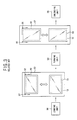
- FIG. 1 illustrates a cross-sectional view of a first mother substrate having thin film transistor array substrates and a second mother substrate having color filter substrates, in which the first and second mother substrates are bonded to each other to construct a plurality of liquid crystal display panels.
- each of thin film transistor array substrates 1 has one side protruding longer than that of each of corresponding color filter substrates 2 . This is because gate and data pad parts(not shown in the drawing) are formed at the corresponding edges of the thin film transistor array substrate 1 that are not overlapped by the color filter substrate 2 .
- the color filter substrates 2 on the second mother substrate 30 are separated from each other by a dummy area 31 that corresponds to the area of each of the thin film transistor array substrates 1 on the first mother substrate 20 that does not overlap the color filter substrate 2 .
- the unit liquid crystal display panels are arranged properly to make best use of the first and second mother substrates 20 and 30 .
- the unit liquid crystal display panels are generally formed to be separated from each other by an area of another dummy area 32 .
- the liquid crystal display panels are individually cut.
- the dummy area 31 of each of the color filter substrates 2 of the second mother substrate 30 and the other dummy area 32 separating the unit liquid crystal display panels from each other are removed simultaneously.
- FIG. 2 illustrates a schematic layout of an individually cut unit liquid crystal display panel according to a related art.
- a unit liquid crystal display panel 10 includes an image display part 13 having liquid crystal cells arranged in a matrix form, a gate pad part 14 connecting gate lines GL 1 ⁇ GLm of the image display part 13 to a gate driver integrated circuit(not shown in the drawing) for supplying gate signals, and a data pad part 15 connecting data lines DL 1 ⁇ DLn of the image display part 13 to a data driver integrated circuit(not shown in the drawing) for supplying image information.
- the gate and data pad parts 14 and 15 are formed on edge areas of a thin film transistor array substrate 1 having long sides and short sides protruding longer than those of a color filter substrate 2 .
- the data and gate lines DL 1 ⁇ DLn and GL 1 ⁇ GLm cross each other on the thin film transistor array substrate 1 .
- Thin film transistors TFTs are formed at the crossings of the gate and data lines to switch respective liquid crystal cells.
- Pixel electrodes are connected to the thin film transistors to apply electric fields to the corresponding liquid crystal cells, and a passivation layer is formed on an entire surface to protect the data lines DL 1 ⁇ DLn, gate lines GL 1 ⁇ GLm, thin film transistors, and electrodes.
- Color filters are formed on the color filter substrate 2 and are separated from adjacent cells by a black matrix.
- a common electrode is also formed on the color filter substrate 2 as a counter electrode of the pixel electrodes on the thin film transistor array substrate 1 .
- a cell gap is provided between thin film transistor array and color filter substrates 1 and 2 , which face each other, to leave a predetermined interval between them.
- the thin film transistor array and color filter substrates 1 and 2 are bonded to each other by a sealing part(not shown in the drawing) formed on a periphery of the image display part 13 .
- a liquid crystal layer(not shown in the drawing) is formed in the cell gap.
- a short-circuiting line number (not shown in the drawing) is formed on an edge of the thin film transistor array substrate 1 in order to prevent static electricity generated by the patterned conductive layers on the thin film transistor array substrate 1 .
- the short-circuiting line should be removed after the liquid crystal display panels are cut into individual unit liquid crystal display panels.
- edges of the unit liquid crystal display panel are ground to remove the short-circuiting line. Moreover, the edges of the unit liquid crystal display panel are ground to prevent the edges from being torn apart by an external impact as well as the danger of hurting an operator with the sharp edges of the unit liquid crystal display panel.
- FIG. 3 illustrates a block diagram of a device for grinding a liquid crystal display panel according to a related art.
- a device for grinding a liquid crystal display panel includes a loading unit 50 for loading a unit liquid crystal display panel 10 , a first grinding unit 53 for receiving the unit liquid crystal display panel 10 loaded by the loading unit 50 on a first grinding table 51 and for grinding short sides of the unit liquid crystal display panel 10 through a first grinding wheel 52 , a turning unit 54 for turning the unit liquid crystal display panel 10 by 90° after its short sides have been ground, a second grinding unit 57 for receiving the turned unit liquid crystal display panel 10 on a second grinding table 55 and for grinding long sides of the unit liquid crystal display panel 10 through a second grinding wheel 56 , an unloading unit 58 for receiving to unload the unit liquid crystal display panel 10 after its long sides have been ground.
- the first grinding unit 53 grinds the short sides of the unit liquid crystal display panel 10 ; then, the turning unit 54 turns the unit liquid crystal display panel 10 having the grinded short sides by 90°, and the second grinding unit 57 grinds the long sides of the unit liquid crystal display panel 10 .
- the device for grinding the liquid crystal display panel according to the related art has the first grinding unit grind the short sides of the unit liquid crystal display panel and has the second grinding unit grind the long sides of the unit liquid crystal display panel. If the first or second grinding unit is broken or malfunctions, the related art grinding device cannot grind all edges of the unit liquid crystal display panel until it is fixed. Hence, the device for grinding the liquid crystal display panel according to the related art has a reduced efficiency thereby decreasing productivity.
- the present invention is directed to a device for grinding a liquid crystal display panel that substantially obviates one or more problems due to limitations and disadvantages of the related art.
- An advantage of the present invention is to provide a device for grinding a liquid crystal display panel to improve an equipment using efficiency by independently operating first and second grinding units for grinding the unit liquid crystal display panel.
- a device for grinding a liquid crystal display panel includes a first grinding unit for grinding edges of one of short and long sides of the unit liquid crystal display panel in a normal mode and a second grinding unit for grinding the edges of the other of the short and long sides of the unit liquid crystal display panel and for grinding the edges of the long and short sides of the unit liquid crystal display panel in an emergency mode.
- FIG. 1 illustrates a cross-sectional view of a first mother substrate having thin film transistor array substrates and a second mother substrate having color filter substrates according to a related art, in which the first and second mother substrates are bonded to each other to construct a plurality of unit liquid crystal display panels;
- FIG. 2 illustrates a schematic layout of an individually cut unit liquid crystal display panel according to a related art
- FIG. 3 illustrates a block diagram of a device for grinding a liquid crystal display panel according to a related art
- FIG. 4 illustrates a block diagram of a device for grinding a liquid crystal display panel according to one embodiment of the present invention
- FIG. 5 illustrates a block diagram of a device for grinding a liquid crystal display panel in FIG. 4 for explaining operation of the device in a normal mode
- FIG. 6 illustrates a block diagram of a device for grinding a liquid crystal display panel in FIG. 4 for explaining operation of the device in an emergency mode when a second grinding unit is broken or malfunctions;
- FIG. 7 illustrates a block diagram of a device for grinding a liquid crystal display panel in FIG. 4 for explaining operation of the device in an emergency mode when a first grinding unit is broken or malfunctions.
- FIG. 4 illustrates a block diagram of a device for grinding a liquid crystal display panel according to one embodiment of the present invention.
- a device for grinding a liquid crystal display panel includes a loading unit 111 loading a liquid crystal display panel, and a first grinding unit 115 receiving the unit liquid crystal display panel on a first grinding table 112 and grinding edges of short sides of the unit liquid crystal display panel through a first grinding wheel 113 in a normal mode.
- the first grinding unit can also grind the edges of the short sides and edges of long sides of the unit liquid crystal display panel through the first grinding wheel 113 and a second grinding wheel 114 , respectively, in an emergency mode.
- the device for grinding also includes a turning unit 116 turning the unit liquid crystal display panel by 90° after the edges of the short sides have been ground in the first grinding unit 115 , in the normal mode; a second grinding unit 120 receiving the unit liquid crystal display panel turned by the turning unit 116 and grinding the edges of the long sides of the unit liquid crystal display panel through a third grinding wheel 118 in the normal mode.
- the second grinding unit can also grind the edges of the long and short sides of the unit liquid crystal display panel through the third grinding wheel 118 and a fourth grinding wheel 119 respectively in the emergency mode; and an unloading unit 121 receiving the unit liquid crystal display panel after the edges of the short and long sides have been ground by the first and second grinding units 115 and 120 in the normal mode or by the first and second grinding units 115 and 120 in the emergency mode.
- a plurality of suction holes 122 for absorbing the unit liquid crystal display panel effectively by suction are preferably formed on surfaces of the first and second grinding tables 112 and 117 of the first and second grinding units 115 and 120 , respectively.
- FIG. 5 illustrates a block diagram of a device for grinding a liquid crystal display panel in FIG. 4 for explaining operation of the device in a normal mode. Operation of the device of the present embodiment to grind the liquid crystal display panel in a normal mode is the same as operation of the device according to the related art.
- the first grinding unit 115 receives the unit liquid crystal display panel 100 loaded on the loading unit 111 to align on the first grinding unit 115 , and then grinds the edges of the short or long sides of the unit liquid crystal display panel 100 .
- the edges of the short sides of the unit liquid crystal display panel 100 are ground.
- the turning unit 116 turns the unit liquid crystal display panel 100 by 90° after the short sides have been ground by the first grinding unit 115 .
- the second grinding unit 120 receives the unit liquid crystal display panel 100 turned by the turning unit 116 to align on the second grinding table 117 and then grinds the edges of the long or short sides of the unit liquid crystal display panel 100 that were not ground by the first grinding unit 115 through the third grinding wheel 118 .
- the edges of the long sides of the unit liquid crystal display panel 100 are ground.
- the long sides may be ground first by the first grinding unit and then the short sides may be ground by the second grinding unit.
- the unloading unit 121 unloads the unit liquid crystal display panel 100 .
- the device for grinding the unit liquid crystal display panel according to the embodiment of the present invention is driven in the emergency mode.
- FIG. 6 illustrates a block diagram of a device for grinding a liquid crystal display panel in FIG. 4 for explaining that the device operates in an emergency mode when a second grinding unit is broken or malfunctions.
- the first grinding unit 115 receives the unit liquid crystal display panel 100 loaded on the loading unit 111 to align the liquid crystal display panel 100 on the first grinding table 112 , and then grinds the edges of the short and long sides of the unit liquid crystal display panel 100 through the first and second grinding wheels 113 and 114 .
- the unloading unit 121 receives to unload the unit liquid crystal display panel 100 after the edges of the short and long sides have been ground by the first grinding unit 115 .
- FIG. 7 illustrates a block diagram of a device for grinding a liquid crystal display panel in FIG. 4 for explaining that the device operates in an emergency mode when a first grinding unit is broken or malfunctions.
- the second grinding unit 116 receives the unit liquid crystal display panel 100 loaded on the loading unit 111 through the turning unit 116 to align unit liquid crystal display panel 100 on the second grinding table 117 , and then grinds the edges of the long and short sides of the unit liquid crystal display panel 100 through the third and fourth grinding wheels 118 and 119 .
- the unloading unit 121 unloads the unit liquid crystal display panel 100 after the edges of the short and long sides have been ground by the second grinding unit 120 .
- the first grinding unit grinds the edges of the long sides of the unit liquid crystal display panel and the second grinding unit grinds the edges of the short or long sides of the unit liquid crystal display panel that were not ground by the first grinding unit. Therefore, the present invention maximizes productivity.
- the present invention can perform the grinding process through the normally operating second or first grinding unit even if the first or second grinding unit cannot be operated. Therefore, the present invention maximizes the use of the equipment, thereby improving productivity.
Abstract
Description
Claims (17)
Priority Applications (1)
| Application Number | Priority Date | Filing Date | Title |
|---|---|---|---|
| US10/851,176 US7179155B2 (en) | 2002-03-21 | 2004-05-24 | Device for grinding liquid crystal display panel |
Applications Claiming Priority (2)
| Application Number | Priority Date | Filing Date | Title |
|---|---|---|---|
| KR1020020015452A KR100841623B1 (en) | 2002-03-21 | 2002-03-21 | Grinder of liquid crystal display panel |
| KR2002-15452 | 2002-03-21 |
Related Child Applications (1)
| Application Number | Title | Priority Date | Filing Date |
|---|---|---|---|
| US10/851,176 Continuation US7179155B2 (en) | 2002-03-21 | 2004-05-24 | Device for grinding liquid crystal display panel |
Publications (2)
| Publication Number | Publication Date |
|---|---|
| US20030181130A1 US20030181130A1 (en) | 2003-09-25 |
| US6755724B2 true US6755724B2 (en) | 2004-06-29 |
Family
ID=28036158
Family Applications (2)
| Application Number | Title | Priority Date | Filing Date |
|---|---|---|---|
| US10/327,085 Expired - Lifetime US6755724B2 (en) | 2002-03-21 | 2002-12-24 | Device for grinding liquid crystal display panel |
| US10/851,176 Expired - Lifetime US7179155B2 (en) | 2002-03-21 | 2004-05-24 | Device for grinding liquid crystal display panel |
Family Applications After (1)
| Application Number | Title | Priority Date | Filing Date |
|---|---|---|---|
| US10/851,176 Expired - Lifetime US7179155B2 (en) | 2002-03-21 | 2004-05-24 | Device for grinding liquid crystal display panel |
Country Status (4)
| Country | Link |
|---|---|
| US (2) | US6755724B2 (en) |
| JP (1) | JP4118164B2 (en) |
| KR (1) | KR100841623B1 (en) |
| CN (1) | CN1320389C (en) |
Cited By (6)
| Publication number | Priority date | Publication date | Assignee | Title |
|---|---|---|---|---|
| US20030181149A1 (en) * | 2002-03-20 | 2003-09-25 | Sang-Sun Shin | Grinding table for liquid crystal display panel and grinder apparatus using the same |
| US20050026541A1 (en) * | 2003-07-29 | 2005-02-03 | Allaire Roger A. | Pressure feed grinding of AMLCD substrate edges |
| US20060286907A1 (en) * | 2005-06-20 | 2006-12-21 | Hwang Young M | Grinder wheel for liquid crystal display device and method of fabricating liquid crystal display device using the same |
| US8178878B2 (en) | 2008-06-06 | 2012-05-15 | Chimei Innolux Corporation | Mother thin film transistor array substrate and thin film transistor array substrate fabricated therefrom |
| US20130083457A1 (en) * | 2011-09-30 | 2013-04-04 | Apple Inc. | System and method for manufacturing a display panel or other patterned device |
| US8721392B2 (en) | 2011-06-28 | 2014-05-13 | Corning Incorporated | Glass edge finishing method |
Families Citing this family (11)
| Publication number | Priority date | Publication date | Assignee | Title |
|---|---|---|---|---|
| KR100796447B1 (en) * | 2006-07-10 | 2008-01-22 | 주식회사 엔씨비네트웍스 | Grinding device for display panel |
| KR100838108B1 (en) * | 2007-02-12 | 2008-06-13 | 주식회사 케이엔제이 | Menufacturing apparatus for flat panel disply panel and menufacturing method using the same |
| KR101058185B1 (en) * | 2008-05-28 | 2011-08-22 | 주식회사 에스에프에이 | Chamfering machine for flat panel display and processing method |
| KR101165208B1 (en) * | 2009-11-18 | 2012-07-16 | 주식회사 케이엔제이 | Method for grinding flat pannel display |
| KR101223675B1 (en) | 2009-11-27 | 2013-01-17 | 주식회사 케이씨씨 | Saline soluble ceramic fiber composition |
| KR101083259B1 (en) * | 2010-10-07 | 2011-11-14 | 유지헌 | Grinding apparatus for reuse mold |
| KR101974379B1 (en) | 2012-05-22 | 2019-09-06 | 삼성디스플레이 주식회사 | Substrate griding appatus and method thereof |
| CN102672624B (en) * | 2012-06-05 | 2015-02-11 | 禾睿联科技(厦门)有限公司 | Device for removing burrs |
| KR101513906B1 (en) * | 2014-02-12 | 2015-04-21 | (주)미래컴퍼니 | Apparatus and method for processing panel |
| CN105014490A (en) * | 2015-06-24 | 2015-11-04 | 林嘉佑 | Manufacturing method for optical glass |
| CN110587469A (en) * | 2019-09-29 | 2019-12-20 | 苏州光斯奥光电科技有限公司 | Grinding mechanism for liquid crystal panel |
Citations (160)
| Publication number | Priority date | Publication date | Assignee | Title |
|---|---|---|---|---|
| JPS5165656A (en) | 1974-12-04 | 1976-06-07 | Shinshu Seiki Kk | |
| US3978580A (en) | 1973-06-28 | 1976-09-07 | Hughes Aircraft Company | Method of fabricating a liquid crystal display |
| US4094058A (en) | 1976-07-23 | 1978-06-13 | Omron Tateisi Electronics Co. | Method of manufacture of liquid crystal displays |
| JPS5738414A (en) | 1980-08-20 | 1982-03-03 | Showa Denko Kk | Spacer for display panel |
| JPS5788428A (en) | 1980-11-20 | 1982-06-02 | Ricoh Elemex Corp | Manufacture of liquid crystal display body device |
| JPS5827126A (en) | 1981-08-11 | 1983-02-17 | Nec Corp | Production of liquid crystal display panel |
| JPS5957221A (en) | 1982-09-28 | 1984-04-02 | Asahi Glass Co Ltd | Production of display element |
| JPS59195222A (en) | 1983-04-19 | 1984-11-06 | Matsushita Electric Ind Co Ltd | Manufacture of liquid-crystal panel |
| JPS60111221A (en) | 1983-11-19 | 1985-06-17 | Nippon Denso Co Ltd | Method and device for charging liquid crystal |
| JPS60164723A (en) | 1984-02-07 | 1985-08-27 | Seiko Instr & Electronics Ltd | Liquid crystal display device |
| JPS60217343A (en) | 1984-04-13 | 1985-10-30 | Matsushita Electric Ind Co Ltd | Liquid crystal display device and its preparation |
| JPS617822A (en) | 1984-06-22 | 1986-01-14 | Canon Inc | Production of liquid crystal element |
| JPS6155625A (en) | 1984-08-24 | 1986-03-20 | Nippon Denso Co Ltd | Manufacture of liquid crystal element |
| US4653864A (en) | 1986-02-26 | 1987-03-31 | Ovonic Imaging Systems, Inc. | Liquid crystal matrix display having improved spacers and method of making same |
| JPS6289025A (en) | 1985-10-15 | 1987-04-23 | Matsushita Electric Ind Co Ltd | Liquid crystal display panel and its production |
| JPS6290622A (en) | 1985-10-17 | 1987-04-25 | Seiko Epson Corp | Liquid crystal display device |
| US4685180A (en) * | 1984-07-19 | 1987-08-11 | Nippon Sheet Glass Co., Ltd. | Contour shaping apparatus |
| US4691995A (en) | 1985-07-15 | 1987-09-08 | Semiconductor Energy Laboratory Co., Ltd. | Liquid crystal filling device |
| JPS62205319A (en) | 1986-03-06 | 1987-09-09 | Canon Inc | Ferroelectric liquid crystal element |
| JPS63109413A (en) | 1986-10-27 | 1988-05-14 | Fujitsu Ltd | Production of liquid crystal display |
| JPS63110425A (en) | 1986-10-29 | 1988-05-14 | Toppan Printing Co Ltd | Cell for sealing liquid crystal |
| JPS63128315A (en) | 1986-11-19 | 1988-05-31 | Victor Co Of Japan Ltd | Liquid crystal display element |
| US4775225A (en) | 1985-05-16 | 1988-10-04 | Canon Kabushiki Kaisha | Liquid crystal device having pillar spacers with small base periphery width in direction perpendicular to orientation treatment |
| JPS63311233A (en) | 1987-06-12 | 1988-12-20 | Toyota Motor Corp | Liquid crystal cell |
| JPH05127179A (en) | 1991-11-01 | 1993-05-25 | Ricoh Co Ltd | Production of liquid crystal display element |
| JPH05154923A (en) | 1991-12-06 | 1993-06-22 | Hitachi Ltd | Substrate assembling device |
| US5247377A (en) | 1988-07-23 | 1993-09-21 | Rohm Gmbh Chemische Fabrik | Process for producing anisotropic liquid crystal layers on a substrate |
| JPH05265011A (en) | 1992-03-19 | 1993-10-15 | Seiko Instr Inc | Production of liquid crystal display element |
| JPH05281557A (en) | 1992-04-01 | 1993-10-29 | Matsushita Electric Ind Co Ltd | Manufacture of liquid crystal panel |
| JPH05281562A (en) | 1992-04-01 | 1993-10-29 | Matsushita Electric Ind Co Ltd | Manufacture of liquid crystal panel |
| US5263888A (en) | 1992-02-20 | 1993-11-23 | Matsushita Electric Industrial Co., Ltd. | Method of manufacture of liquid crystal display panel |
| JPH0651256A (en) | 1992-07-30 | 1994-02-25 | Matsushita Electric Ind Co Ltd | Device for discharging liquid crystal |
| JPH06148657A (en) | 1992-11-06 | 1994-05-27 | Matsushita Electric Ind Co Ltd | Method and device for manufacturing cell for liquid crystal display |
| JPH06160871A (en) | 1992-11-26 | 1994-06-07 | Matsushita Electric Ind Co Ltd | Liquid crystal display panel and its production |
| JPH06235925A (en) | 1993-02-10 | 1994-08-23 | Matsushita Electric Ind Co Ltd | Manufacture of liquid crystal display element |
| JPH06265915A (en) | 1993-03-12 | 1994-09-22 | Matsushita Electric Ind Co Ltd | Discharge device for filling liquid crystal |
| JPH06313870A (en) | 1993-04-28 | 1994-11-08 | Hitachi Ltd | Substrate assembly device |
| US5379139A (en) | 1986-08-20 | 1995-01-03 | Semiconductor Energy Laboratory Co., Ltd. | Liquid crystal device and method for manufacturing same with spacers formed by photolithography |
| JPH0784268A (en) | 1993-09-13 | 1995-03-31 | Hitachi Ltd | Method for plotting sealing material |
| US5406989A (en) | 1993-10-12 | 1995-04-18 | Ayumi Industry Co., Ltd. | Method and dispenser for filling liquid crystal into LCD cell |
| JPH07128674A (en) | 1993-11-05 | 1995-05-19 | Matsushita Electric Ind Co Ltd | Production of liquid crystal display element |
| JPH07181507A (en) | 1993-12-21 | 1995-07-21 | Canon Inc | Liquid crystal display device and information transmission device having the liquid crystal display device |
| US5499128A (en) | 1993-03-15 | 1996-03-12 | Kabushiki Kaisha Toshiba | Liquid crystal display device with acrylic polymer spacers and method of manufacturing the same |
| JPH0895066A (en) | 1994-09-27 | 1996-04-12 | Matsushita Electric Ind Co Ltd | Manufacture of liquid crystal element and device thereof |
| US5507323A (en) | 1993-10-12 | 1996-04-16 | Fujitsu Limited | Method and dispenser for filling liquid crystal into LCD cell |
| JPH08101395A (en) | 1994-09-30 | 1996-04-16 | Matsushita Electric Ind Co Ltd | Production of liquid crystal display element |
| JPH08106101A (en) | 1994-10-06 | 1996-04-23 | Fujitsu Ltd | Production of liquid crystal display panel |
| JPH08171094A (en) | 1994-12-19 | 1996-07-02 | Nippon Soken Inc | Liquid crystal injecting method and liquid crystal injecting device to liquid crystal display device |
| US5539545A (en) | 1993-05-18 | 1996-07-23 | Semiconductor Energy Laboratory Co., Ltd. | Method of making LCD in which resin columns are cured and the liquid crystal is reoriented |
| JPH08190099A (en) | 1995-01-11 | 1996-07-23 | Fujitsu Ltd | Production of liquid crystal display device and apparatus for producing liquid crystal display device |
| US5548429A (en) | 1993-06-14 | 1996-08-20 | Canon Kabushiki Kaisha | Process for producing liquid crystal device whereby curing the sealant takes place after pre-baking the substrates |
| JPH08240807A (en) | 1995-03-06 | 1996-09-17 | Fujitsu Ltd | Method for sealing liquid crystal display panel |
| JPH095762A (en) | 1995-06-20 | 1997-01-10 | Matsushita Electric Ind Co Ltd | Production of liquid crystal panel |
| JPH0926578A (en) | 1995-07-10 | 1997-01-28 | Fujitsu Ltd | Liquid crystal display panel and manufacture thereof |
| JPH0961829A (en) | 1995-08-21 | 1997-03-07 | Matsushita Electric Ind Co Ltd | Production of liquid crystal display element |
| JPH0973096A (en) | 1995-09-05 | 1997-03-18 | Matsushita Electric Ind Co Ltd | Production of liquid crystal display device |
| JPH0973075A (en) | 1995-09-05 | 1997-03-18 | Matsushita Electric Ind Co Ltd | Production of liquid crystal display element and apparatus for producing liquid crystal display element |
| JPH09127528A (en) | 1995-10-27 | 1997-05-16 | Fujitsu Ltd | Production of liquid crystal panel |
| US5642214A (en) | 1991-07-19 | 1997-06-24 | Sharp Kabushiki Kaisha | Optical modulating element and electronic apparatus using it |
| JPH09230357A (en) | 1996-02-22 | 1997-09-05 | Canon Inc | Production of liquid crystal panel and liquid crystal cell used for the same |
| JPH09281511A (en) | 1996-04-17 | 1997-10-31 | Fujitsu Ltd | Production of liquid crystal display panel |
| JPH09311340A (en) | 1996-05-21 | 1997-12-02 | Matsushita Electric Ind Co Ltd | Manufacture of liquid crystal display device |
| US5742370A (en) | 1996-09-12 | 1998-04-21 | Korea Institute Of Science And Technology | Fabrication method for liquid crystal alignment layer by magnetic field treatment |
| JPH10123538A (en) | 1996-10-22 | 1998-05-15 | Matsushita Electric Ind Co Ltd | Production for liquid crystal display element |
| JPH10123537A (en) | 1996-10-15 | 1998-05-15 | Matsushita Electric Ind Co Ltd | Liquid crystal display element and its production |
| US5757451A (en) | 1995-09-08 | 1998-05-26 | Kabushiki Kaisha Toshiba | Liquid crystal display device spacers formed from stacked color layers |
| JPH10142616A (en) | 1996-11-14 | 1998-05-29 | Ayumi Kogyo Kk | Liquid crystal injection method and liquid dispenser |
| JPH10177178A (en) | 1996-12-17 | 1998-06-30 | Matsushita Electric Ind Co Ltd | Production of liquid crystal display element |
| JPH10221700A (en) | 1997-02-10 | 1998-08-21 | Fujitsu Ltd | Liquid crystal display device manufacturing method |
| JPH10282512A (en) | 1997-04-07 | 1998-10-23 | Ayumi Kogyo Kk | Method for injecting liquid crystal and dispenser used for the same |
| JPH10333157A (en) | 1997-06-03 | 1998-12-18 | Matsushita Electric Ind Co Ltd | Manufacture of liquid crystal display device |
| JPH10333159A (en) | 1997-06-03 | 1998-12-18 | Matsushita Electric Ind Co Ltd | Liquid crystal display device |
| US5852484A (en) | 1994-09-26 | 1998-12-22 | Matsushita Electric Industrial Co., Ltd. | Liquid crystal display panel and method and device for manufacturing the same |
| US5861932A (en) | 1997-03-31 | 1999-01-19 | Denso Corporation | Liquid crystal cell and its manufacturing method |
| JPH1114953A (en) | 1997-06-20 | 1999-01-22 | Matsushita Electric Ind Co Ltd | Manufacture of multi-numbered liquid crystal display panel, and multi-numbered liquid crystal panel |
| JPH1138424A (en) | 1997-07-23 | 1999-02-12 | Fujitsu Ltd | Liquid crystal display panel and its production |
| US5875922A (en) | 1997-10-10 | 1999-03-02 | Nordson Corporation | Apparatus for dispensing an adhesive |
| JPH1164811A (en) | 1997-08-21 | 1999-03-05 | Matsushita Electric Ind Co Ltd | Method and device for producing liquid crystal display element |
| JPH11109388A (en) | 1997-10-03 | 1999-04-23 | Hitachi Ltd | Production of liquid crystal display device |
| JPH11133438A (en) | 1997-10-24 | 1999-05-21 | Matsushita Electric Ind Co Ltd | Liquid crystal display element and its production |
| US5952676A (en) | 1986-08-20 | 1999-09-14 | Semiconductor Energy Laboratory Co., Ltd. | Liquid crystal device and method for manufacturing same with spacers formed by photolithography |
| US5956112A (en) | 1995-10-02 | 1999-09-21 | Sharp Kabushiki Kaisha | Liquid crystal display device and method for manufacturing the same |
| US6001203A (en) | 1995-03-01 | 1999-12-14 | Matsushita Electric Industrial Co., Ltd. | Production process of liquid crystal display panel, seal material for liquid crystal cell and liquid crystal display |
| US6011609A (en) | 1996-10-05 | 2000-01-04 | Samsung Electronics Co., Ltd. | Method of manufacturing LCD by dropping liquid crystals on a substrate and then pressing the substrates |
| JP2000002879A (en) | 1998-06-12 | 2000-01-07 | Matsushita Electric Ind Co Ltd | Device for assembling liquid crystal panel and its method |
| US6016181A (en) | 1996-11-07 | 2000-01-18 | Sharp Kabushiki Kaisha | Liquid crystal device having column spacers with portion on each of the spacers for reflecting or absorbing visible light and method for fabricating the same |
| US6016178A (en) | 1996-09-13 | 2000-01-18 | Sony Corporation | Reflective guest-host liquid-crystal display device |
| JP2000029035A (en) | 1998-07-09 | 2000-01-28 | Minolta Co Ltd | Liquid crystal element and its manufacture |
| JP2000056311A (en) | 1998-08-03 | 2000-02-25 | Matsushita Electric Ind Co Ltd | Liquid crystal display device |
| JP2000066165A (en) | 1998-08-20 | 2000-03-03 | Matsushita Electric Ind Co Ltd | Manufacture of liquid crystal display panel |
| US6055035A (en) | 1998-05-11 | 2000-04-25 | International Business Machines Corporation | Method and apparatus for filling liquid crystal display (LCD) panels |
| JP2000137235A (en) | 1998-11-02 | 2000-05-16 | Matsushita Electric Ind Co Ltd | Sticking method of liquid crystal substrate |
| EP1003066A1 (en) | 1998-11-16 | 2000-05-24 | Matsushita Electric Industrial Co., Ltd. | Method of manufacturing liquid crystal display devices |
| JP2000193988A (en) | 1998-12-25 | 2000-07-14 | Fujitsu Ltd | Production of liquid crystal display panel and apparatus for production |
| JP2000241824A (en) | 1999-02-18 | 2000-09-08 | Matsushita Electric Ind Co Ltd | Manufacture of liquid crystal display device |
| JP2000284295A (en) | 1999-03-30 | 2000-10-13 | Hitachi Techno Eng Co Ltd | Method and apparatus for assembling substrate |
| JP2000292799A (en) | 1999-04-09 | 2000-10-20 | Matsushita Electric Ind Co Ltd | Liquid crystal display device and its production |
| JP2000310759A (en) | 1999-04-28 | 2000-11-07 | Matsushita Electric Ind Co Ltd | Device for manufacturing liquid crystal display element and its method |
| JP2000310784A (en) | 1999-02-22 | 2000-11-07 | Matsushita Electric Ind Co Ltd | Liquid crystal panel, color filter and their production |
| JP2000338501A (en) | 1999-05-26 | 2000-12-08 | Matsushita Electric Ind Co Ltd | Production of liquid crystal display panel |
| US6163357A (en) | 1996-09-26 | 2000-12-19 | Kabushiki Kaisha Toshiba | Liquid crystal display device having the driving circuit disposed in the seal area, with different spacer density in driving circuit area than display area |
| JP2001005401A (en) | 1999-06-21 | 2001-01-12 | Hitachi Techno Eng Co Ltd | Method for assembling substrates and device therefor |
| JP2001005405A (en) | 1999-06-18 | 2001-01-12 | Hitachi Techno Eng Co Ltd | Method for assembling substrate and apparatus therefor |
| JP2001013506A (en) | 1999-04-30 | 2001-01-19 | Matsushita Electric Ind Co Ltd | Liquid crystal display element and its manufacture |
| JP2001033793A (en) | 1999-07-21 | 2001-02-09 | Matsushita Electric Ind Co Ltd | Liquid crystal display panel and manufacturing method therefor |
| JP2001042341A (en) | 1999-08-03 | 2001-02-16 | Hitachi Techno Eng Co Ltd | Method for assembling liquid crystal substrate |
| JP2001051284A (en) | 1999-08-10 | 2001-02-23 | Matsushita Electric Ind Co Ltd | Device for manufacturing liquid crystal display device |
| JP2001066615A (en) | 2000-08-02 | 2001-03-16 | Matsushita Electric Ind Co Ltd | Manufacture of liquid crystal display device |
| JP2001091727A (en) | 1999-09-27 | 2001-04-06 | Matsushita Electric Ind Co Ltd | Production method of color filter substrate, color filter substrate and liquid crystal display device |
| US6219126B1 (en) | 1998-11-20 | 2001-04-17 | International Business Machines Corporation | Panel assembly for liquid crystal displays having a barrier fillet and an adhesive fillet in the periphery |
| JP2001117109A (en) | 1999-10-21 | 2001-04-27 | Matsushita Electric Ind Co Ltd | Method of manufacturing for liquid crystal display device |
| JP2001117105A (en) | 1999-10-18 | 2001-04-27 | Toshiba Corp | Method of manufacturing for liquid crystal display device |
| US6226067B1 (en) | 1997-10-03 | 2001-05-01 | Minolta Co., Ltd. | Liquid crystal device having spacers and manufacturing method thereof |
| JP2001133799A (en) | 1999-11-05 | 2001-05-18 | Fujitsu Ltd | Method of producing liquid crystal display device |
| JP2001133745A (en) | 1999-11-08 | 2001-05-18 | Hitachi Techno Eng Co Ltd | Method of assembling substrate and device therefor |
| JP2001133794A (en) | 1999-11-01 | 2001-05-18 | Kyoritsu Kagaku Sangyo Kk | Sealing agent for dropping process of lcd panel |
| US6236445B1 (en) | 1996-02-22 | 2001-05-22 | Hughes Electronics Corporation | Method for making topographic projections |
| JP2001142074A (en) | 1999-11-10 | 2001-05-25 | Hitachi Ltd | Liquid crystal display device |
| JP2001147437A (en) | 1999-11-19 | 2001-05-29 | Nec Corp | Liquid crystal display panel and method of producing the same |
| JP2001154211A (en) | 1999-11-30 | 2001-06-08 | Hitachi Ltd | Liquid crystal panel and its manufacturing method |
| JP2001166310A (en) | 1999-12-08 | 2001-06-22 | Matsushita Electric Ind Co Ltd | Method of producing liquid crystal display panel |
| JP2001166272A (en) | 1999-12-09 | 2001-06-22 | Hitachi Techno Eng Co Ltd | Method and device for assembling substrate |
| JP2001183683A (en) | 1999-10-05 | 2001-07-06 | Matsushita Electric Ind Co Ltd | Liquid crystal panel, its manufacturing and driving method |
| JP2001201750A (en) | 2000-01-14 | 2001-07-27 | Fujitsu Ltd | Liquid crystal display device and method of producing the same |
| JP2001209052A (en) | 2000-01-24 | 2001-08-03 | Matsushita Electric Ind Co Ltd | Liquid crystal display device and its manufacturing method |
| JP2001209060A (en) | 2000-12-11 | 2001-08-03 | Fujitsu Ltd | Method of producing liquid crystal display panel |
| JP2001215459A (en) | 2000-02-02 | 2001-08-10 | Matsushita Electric Ind Co Ltd | Divice for manufacturing liquid crystal display element |
| JP2001222017A (en) | 1999-05-24 | 2001-08-17 | Fujitsu Ltd | Liquid crystal display device and its manufacturing method |
| JP2001235758A (en) | 2000-02-23 | 2001-08-31 | Fujitsu Ltd | Liquid crystal display panel and its manufacturing method |
| JP2001255542A (en) | 2000-03-14 | 2001-09-21 | Sharp Corp | Method and device for laminating substrate and method and device for manufacturing liquid crystal display device |
| JP2001264782A (en) | 2000-03-16 | 2001-09-26 | Ayumi Kogyo Kk | Method of filling gap of flat panel substrate with viscous liquid material |
| JP2001272640A (en) | 2000-03-27 | 2001-10-05 | Fujitsu Ltd | Liquid crystal dropping device and liquid crystal dropping method |
| JP2001281678A (en) | 2000-03-29 | 2001-10-10 | Fujitsu Ltd | Method of manufacturing liquid crystal display device |
| JP2001281675A (en) | 2000-03-29 | 2001-10-10 | Matsushita Electric Ind Co Ltd | Production method for liquid crystal display device |
| JP2001282126A (en) | 2000-03-30 | 2001-10-12 | Hitachi Techno Eng Co Ltd | Substrate assembling device |
| US6304306B1 (en) | 1995-02-17 | 2001-10-16 | Sharp Kabushiki Kaisha | Liquid crystal display device and method for producing the same |
| JP2001305563A (en) | 2000-04-19 | 2001-10-31 | Hitachi Techno Eng Co Ltd | Substrate sticking device |
| US6319100B1 (en) * | 1999-05-13 | 2001-11-20 | Fujikoshi Kikai Kogyo Kabushiki Kaisha | Disk edge polishing machine and disk edge polishing system |
| JP2001330840A (en) | 2000-05-18 | 2001-11-30 | Toshiba Corp | Method for manufacturing liquid crystal display element |
| JP2001330837A (en) | 2000-05-19 | 2001-11-30 | Matsushita Electric Ind Co Ltd | Hermetic structural, its manufacturing method, liquid crystal display device using the same and its manufacturing method |
| US6325704B1 (en) * | 1999-06-14 | 2001-12-04 | Corning Incorporated | Method for finishing edges of glass sheets |
| JP2001356353A (en) | 2001-04-24 | 2001-12-26 | Hitachi Industries Co Ltd | Assembly device for substrate |
| JP2001356354A (en) | 2000-06-13 | 2001-12-26 | Matsushita Electric Ind Co Ltd | Method for manufacturing liquid crystal display device |
| US6337730B1 (en) | 1998-06-02 | 2002-01-08 | Denso Corporation | Non-uniformly-rigid barrier wall spacers used to correct problems caused by thermal contraction of smectic liquid crystal material |
| JP2002014360A (en) | 2000-06-29 | 2002-01-18 | Matsushita Electric Ind Co Ltd | Method and device for manufacturing liquid crystal panel |
| JP2002023176A (en) | 2000-07-05 | 2002-01-23 | Seiko Epson Corp | Liquid crystal filling system and method for filling liquid crystal |
| JP2002049045A (en) | 2000-08-03 | 2002-02-15 | Nec Corp | Method for manufacturing liquid crystal display panel |
| JP2002082340A (en) | 2000-09-08 | 2002-03-22 | Fuji Xerox Co Ltd | Method for manufacturing flat panel display |
| US6361867B2 (en) * | 1996-03-19 | 2002-03-26 | Fujitsu Limited | Laminated glass substrate structure and its manufacture |
| JP2002090760A (en) | 2000-09-12 | 2002-03-27 | Matsushita Electric Ind Co Ltd | Apparatus and method for manufacturing liquid crystal display panel |
| JP2002090759A (en) | 2000-09-18 | 2002-03-27 | Sharp Corp | Apparatus and method for manufacturing liquid crystal display element |
| JP2002107740A (en) | 2000-09-28 | 2002-04-10 | Sharp Corp | Method and device for manufacturing liquid crystal display panel |
| JP2002122873A (en) | 2000-10-13 | 2002-04-26 | Stanley Electric Co Ltd | Method of manufacturing liquid crystal display device |
| JP2002122872A (en) | 2000-10-12 | 2002-04-26 | Hitachi Ltd | Liquid crystal display device and method of manufacturing the same |
| JP2002139734A (en) | 2000-10-31 | 2002-05-17 | Fujitsu Ltd | Manufacturing method and manufacturing device of liquid crystal display device |
| US6414733B1 (en) | 1999-02-08 | 2002-07-02 | Dai Nippon Printing Co., Ltd. | Color liquid crystal display with a shielding member being arranged between sealing member and display zone |
| JP2002202514A (en) | 2000-12-28 | 2002-07-19 | Matsushita Electric Ind Co Ltd | Liquid crystal panel, and method and manufacturing apparatus for manufacturing the same |
| JP2002202512A (en) | 2000-12-28 | 2002-07-19 | Toshiba Corp | Liquid crystal display device and method of manufacturing for the same |
| JP2002214626A (en) | 2001-01-17 | 2002-07-31 | Toshiba Corp | Manufacturing method and sealing material for liquid crystal display |
| US6565421B1 (en) * | 1999-09-01 | 2003-05-20 | Lg Philips Lcd Co., Ltd. | Apparatus and method of grinding liquid crystal cell |
Family Cites Families (12)
| Publication number | Priority date | Publication date | Assignee | Title |
|---|---|---|---|---|
| JPS5766845A (en) * | 1980-10-03 | 1982-04-23 | Fuji Electric Co Ltd | Nc work apparatus |
| JP3319782B2 (en) * | 1991-10-11 | 2002-09-03 | 三星ダイヤモンド工業株式会社 | Glass polishing equipment |
| JP2983836B2 (en) * | 1994-04-25 | 1999-11-29 | 三星ダイヤモンド工業株式会社 | Electrode terminal treatment method |
| JPH08197402A (en) * | 1995-01-25 | 1996-08-06 | Mitsuboshi Daiyamondo Kogyo Kk | Polishing method and device for glass substrate |
| JPH10118907A (en) * | 1996-10-15 | 1998-05-12 | Hitachi Electron Eng Co Ltd | Outer periphery processing device of glass substrate |
| US5878922A (en) * | 1997-07-09 | 1999-03-09 | Sunoco Products Company | Self venting plunger |
| JPH11245151A (en) * | 1998-02-27 | 1999-09-14 | Speedfam Co Ltd | Work periphery polishing device |
| JP3132468B2 (en) * | 1998-05-20 | 2001-02-05 | 日本電気株式会社 | Semiconductor wafer polishing apparatus and polishing method therefor |
| JP3825220B2 (en) * | 1999-02-04 | 2006-09-27 | アプライド マテリアルズ インコーポレイテッド | Chemical mechanical polishing using moving abrasive sheet |
| KR20010045994A (en) * | 1999-11-09 | 2001-06-05 | 윤종용 | Chemical mechanical polishing apparatus having multiple polishing pads |
| JP2001217214A (en) * | 2000-02-03 | 2001-08-10 | Meiji Kikai Kk | Fully automatic two-platen polishing device |
| KR100425471B1 (en) * | 2001-11-10 | 2004-03-30 | 삼성전자주식회사 | Treatment apparatus for grinding and polishing backside of wafer |
-
2002
- 2002-03-21 KR KR1020020015452A patent/KR100841623B1/en active IP Right Grant
- 2002-12-24 US US10/327,085 patent/US6755724B2/en not_active Expired - Lifetime
-
2003
- 2003-02-20 CN CNB031054013A patent/CN1320389C/en not_active Expired - Lifetime
- 2003-02-26 JP JP2003049538A patent/JP4118164B2/en not_active Expired - Lifetime
-
2004
- 2004-05-24 US US10/851,176 patent/US7179155B2/en not_active Expired - Lifetime
Patent Citations (166)
| Publication number | Priority date | Publication date | Assignee | Title |
|---|---|---|---|---|
| US3978580A (en) | 1973-06-28 | 1976-09-07 | Hughes Aircraft Company | Method of fabricating a liquid crystal display |
| JPS5165656A (en) | 1974-12-04 | 1976-06-07 | Shinshu Seiki Kk | |
| US4094058A (en) | 1976-07-23 | 1978-06-13 | Omron Tateisi Electronics Co. | Method of manufacture of liquid crystal displays |
| JPS5738414A (en) | 1980-08-20 | 1982-03-03 | Showa Denko Kk | Spacer for display panel |
| JPS5788428A (en) | 1980-11-20 | 1982-06-02 | Ricoh Elemex Corp | Manufacture of liquid crystal display body device |
| JPS5827126A (en) | 1981-08-11 | 1983-02-17 | Nec Corp | Production of liquid crystal display panel |
| JPS5957221A (en) | 1982-09-28 | 1984-04-02 | Asahi Glass Co Ltd | Production of display element |
| JPS59195222A (en) | 1983-04-19 | 1984-11-06 | Matsushita Electric Ind Co Ltd | Manufacture of liquid-crystal panel |
| JPS60111221A (en) | 1983-11-19 | 1985-06-17 | Nippon Denso Co Ltd | Method and device for charging liquid crystal |
| JPS60164723A (en) | 1984-02-07 | 1985-08-27 | Seiko Instr & Electronics Ltd | Liquid crystal display device |
| JPS60217343A (en) | 1984-04-13 | 1985-10-30 | Matsushita Electric Ind Co Ltd | Liquid crystal display device and its preparation |
| JPS617822A (en) | 1984-06-22 | 1986-01-14 | Canon Inc | Production of liquid crystal element |
| US4685180A (en) * | 1984-07-19 | 1987-08-11 | Nippon Sheet Glass Co., Ltd. | Contour shaping apparatus |
| JPS6155625A (en) | 1984-08-24 | 1986-03-20 | Nippon Denso Co Ltd | Manufacture of liquid crystal element |
| US4775225A (en) | 1985-05-16 | 1988-10-04 | Canon Kabushiki Kaisha | Liquid crystal device having pillar spacers with small base periphery width in direction perpendicular to orientation treatment |
| US4691995A (en) | 1985-07-15 | 1987-09-08 | Semiconductor Energy Laboratory Co., Ltd. | Liquid crystal filling device |
| JPS6289025A (en) | 1985-10-15 | 1987-04-23 | Matsushita Electric Ind Co Ltd | Liquid crystal display panel and its production |
| JPS6290622A (en) | 1985-10-17 | 1987-04-25 | Seiko Epson Corp | Liquid crystal display device |
| US4653864A (en) | 1986-02-26 | 1987-03-31 | Ovonic Imaging Systems, Inc. | Liquid crystal matrix display having improved spacers and method of making same |
| JPS62205319A (en) | 1986-03-06 | 1987-09-09 | Canon Inc | Ferroelectric liquid crystal element |
| US5379139A (en) | 1986-08-20 | 1995-01-03 | Semiconductor Energy Laboratory Co., Ltd. | Liquid crystal device and method for manufacturing same with spacers formed by photolithography |
| US5952676A (en) | 1986-08-20 | 1999-09-14 | Semiconductor Energy Laboratory Co., Ltd. | Liquid crystal device and method for manufacturing same with spacers formed by photolithography |
| JPS63109413A (en) | 1986-10-27 | 1988-05-14 | Fujitsu Ltd | Production of liquid crystal display |
| JPS63110425A (en) | 1986-10-29 | 1988-05-14 | Toppan Printing Co Ltd | Cell for sealing liquid crystal |
| JPS63128315A (en) | 1986-11-19 | 1988-05-31 | Victor Co Of Japan Ltd | Liquid crystal display element |
| JPS63311233A (en) | 1987-06-12 | 1988-12-20 | Toyota Motor Corp | Liquid crystal cell |
| US5247377A (en) | 1988-07-23 | 1993-09-21 | Rohm Gmbh Chemische Fabrik | Process for producing anisotropic liquid crystal layers on a substrate |
| US5642214A (en) | 1991-07-19 | 1997-06-24 | Sharp Kabushiki Kaisha | Optical modulating element and electronic apparatus using it |
| JPH05127179A (en) | 1991-11-01 | 1993-05-25 | Ricoh Co Ltd | Production of liquid crystal display element |
| JPH05154923A (en) | 1991-12-06 | 1993-06-22 | Hitachi Ltd | Substrate assembling device |
| US5263888A (en) | 1992-02-20 | 1993-11-23 | Matsushita Electric Industrial Co., Ltd. | Method of manufacture of liquid crystal display panel |
| JPH05265011A (en) | 1992-03-19 | 1993-10-15 | Seiko Instr Inc | Production of liquid crystal display element |
| JPH05281557A (en) | 1992-04-01 | 1993-10-29 | Matsushita Electric Ind Co Ltd | Manufacture of liquid crystal panel |
| JPH05281562A (en) | 1992-04-01 | 1993-10-29 | Matsushita Electric Ind Co Ltd | Manufacture of liquid crystal panel |
| US5511591A (en) | 1992-04-13 | 1996-04-30 | Fujitsu Limited | Method and dispenser for filling liquid crystal into LCD cell |
| JPH0651256A (en) | 1992-07-30 | 1994-02-25 | Matsushita Electric Ind Co Ltd | Device for discharging liquid crystal |
| JPH06148657A (en) | 1992-11-06 | 1994-05-27 | Matsushita Electric Ind Co Ltd | Method and device for manufacturing cell for liquid crystal display |
| JPH06160871A (en) | 1992-11-26 | 1994-06-07 | Matsushita Electric Ind Co Ltd | Liquid crystal display panel and its production |
| JPH06235925A (en) | 1993-02-10 | 1994-08-23 | Matsushita Electric Ind Co Ltd | Manufacture of liquid crystal display element |
| JPH06265915A (en) | 1993-03-12 | 1994-09-22 | Matsushita Electric Ind Co Ltd | Discharge device for filling liquid crystal |
| US5499128A (en) | 1993-03-15 | 1996-03-12 | Kabushiki Kaisha Toshiba | Liquid crystal display device with acrylic polymer spacers and method of manufacturing the same |
| JPH06313870A (en) | 1993-04-28 | 1994-11-08 | Hitachi Ltd | Substrate assembly device |
| US5539545A (en) | 1993-05-18 | 1996-07-23 | Semiconductor Energy Laboratory Co., Ltd. | Method of making LCD in which resin columns are cured and the liquid crystal is reoriented |
| US5680189A (en) | 1993-05-18 | 1997-10-21 | Semiconductor Energy Laboratory Co., Ltd. | LCD columnar spacers made of a hydrophilic resin and LCD orientation film having a certain surface tension or alignment capability |
| US5548429A (en) | 1993-06-14 | 1996-08-20 | Canon Kabushiki Kaisha | Process for producing liquid crystal device whereby curing the sealant takes place after pre-baking the substrates |
| JPH0784268A (en) | 1993-09-13 | 1995-03-31 | Hitachi Ltd | Method for plotting sealing material |
| US5406989A (en) | 1993-10-12 | 1995-04-18 | Ayumi Industry Co., Ltd. | Method and dispenser for filling liquid crystal into LCD cell |
| US5507323A (en) | 1993-10-12 | 1996-04-16 | Fujitsu Limited | Method and dispenser for filling liquid crystal into LCD cell |
| JPH07128674A (en) | 1993-11-05 | 1995-05-19 | Matsushita Electric Ind Co Ltd | Production of liquid crystal display element |
| JPH07181507A (en) | 1993-12-21 | 1995-07-21 | Canon Inc | Liquid crystal display device and information transmission device having the liquid crystal display device |
| US5854664A (en) | 1994-09-26 | 1998-12-29 | Matsushita Electric Industrial Co., Ltd. | Liquid crystal display panel and method and device for manufacturing the same |
| US5852484A (en) | 1994-09-26 | 1998-12-22 | Matsushita Electric Industrial Co., Ltd. | Liquid crystal display panel and method and device for manufacturing the same |
| JPH0895066A (en) | 1994-09-27 | 1996-04-12 | Matsushita Electric Ind Co Ltd | Manufacture of liquid crystal element and device thereof |
| JPH08101395A (en) | 1994-09-30 | 1996-04-16 | Matsushita Electric Ind Co Ltd | Production of liquid crystal display element |
| JPH08106101A (en) | 1994-10-06 | 1996-04-23 | Fujitsu Ltd | Production of liquid crystal display panel |
| JPH08171094A (en) | 1994-12-19 | 1996-07-02 | Nippon Soken Inc | Liquid crystal injecting method and liquid crystal injecting device to liquid crystal display device |
| JPH08190099A (en) | 1995-01-11 | 1996-07-23 | Fujitsu Ltd | Production of liquid crystal display device and apparatus for producing liquid crystal display device |
| US6304306B1 (en) | 1995-02-17 | 2001-10-16 | Sharp Kabushiki Kaisha | Liquid crystal display device and method for producing the same |
| US6001203A (en) | 1995-03-01 | 1999-12-14 | Matsushita Electric Industrial Co., Ltd. | Production process of liquid crystal display panel, seal material for liquid crystal cell and liquid crystal display |
| JPH08240807A (en) | 1995-03-06 | 1996-09-17 | Fujitsu Ltd | Method for sealing liquid crystal display panel |
| JPH095762A (en) | 1995-06-20 | 1997-01-10 | Matsushita Electric Ind Co Ltd | Production of liquid crystal panel |
| JPH0926578A (en) | 1995-07-10 | 1997-01-28 | Fujitsu Ltd | Liquid crystal display panel and manufacture thereof |
| JPH0961829A (en) | 1995-08-21 | 1997-03-07 | Matsushita Electric Ind Co Ltd | Production of liquid crystal display element |
| JPH0973096A (en) | 1995-09-05 | 1997-03-18 | Matsushita Electric Ind Co Ltd | Production of liquid crystal display device |
| JPH0973075A (en) | 1995-09-05 | 1997-03-18 | Matsushita Electric Ind Co Ltd | Production of liquid crystal display element and apparatus for producing liquid crystal display element |
| US5757451A (en) | 1995-09-08 | 1998-05-26 | Kabushiki Kaisha Toshiba | Liquid crystal display device spacers formed from stacked color layers |
| US5956112A (en) | 1995-10-02 | 1999-09-21 | Sharp Kabushiki Kaisha | Liquid crystal display device and method for manufacturing the same |
| JPH09127528A (en) | 1995-10-27 | 1997-05-16 | Fujitsu Ltd | Production of liquid crystal panel |
| US6236445B1 (en) | 1996-02-22 | 2001-05-22 | Hughes Electronics Corporation | Method for making topographic projections |
| JPH09230357A (en) | 1996-02-22 | 1997-09-05 | Canon Inc | Production of liquid crystal panel and liquid crystal cell used for the same |
| US6361867B2 (en) * | 1996-03-19 | 2002-03-26 | Fujitsu Limited | Laminated glass substrate structure and its manufacture |
| JPH09281511A (en) | 1996-04-17 | 1997-10-31 | Fujitsu Ltd | Production of liquid crystal display panel |
| JPH09311340A (en) | 1996-05-21 | 1997-12-02 | Matsushita Electric Ind Co Ltd | Manufacture of liquid crystal display device |
| US5742370A (en) | 1996-09-12 | 1998-04-21 | Korea Institute Of Science And Technology | Fabrication method for liquid crystal alignment layer by magnetic field treatment |
| US6016178A (en) | 1996-09-13 | 2000-01-18 | Sony Corporation | Reflective guest-host liquid-crystal display device |
| US6163357A (en) | 1996-09-26 | 2000-12-19 | Kabushiki Kaisha Toshiba | Liquid crystal display device having the driving circuit disposed in the seal area, with different spacer density in driving circuit area than display area |
| US6011609A (en) | 1996-10-05 | 2000-01-04 | Samsung Electronics Co., Ltd. | Method of manufacturing LCD by dropping liquid crystals on a substrate and then pressing the substrates |
| JPH10123537A (en) | 1996-10-15 | 1998-05-15 | Matsushita Electric Ind Co Ltd | Liquid crystal display element and its production |
| JPH10123538A (en) | 1996-10-22 | 1998-05-15 | Matsushita Electric Ind Co Ltd | Production for liquid crystal display element |
| US6016181A (en) | 1996-11-07 | 2000-01-18 | Sharp Kabushiki Kaisha | Liquid crystal device having column spacers with portion on each of the spacers for reflecting or absorbing visible light and method for fabricating the same |
| JPH10142616A (en) | 1996-11-14 | 1998-05-29 | Ayumi Kogyo Kk | Liquid crystal injection method and liquid dispenser |
| JPH10177178A (en) | 1996-12-17 | 1998-06-30 | Matsushita Electric Ind Co Ltd | Production of liquid crystal display element |
| JPH10221700A (en) | 1997-02-10 | 1998-08-21 | Fujitsu Ltd | Liquid crystal display device manufacturing method |
| US5861932A (en) | 1997-03-31 | 1999-01-19 | Denso Corporation | Liquid crystal cell and its manufacturing method |
| JPH10282512A (en) | 1997-04-07 | 1998-10-23 | Ayumi Kogyo Kk | Method for injecting liquid crystal and dispenser used for the same |
| JPH10333159A (en) | 1997-06-03 | 1998-12-18 | Matsushita Electric Ind Co Ltd | Liquid crystal display device |
| JPH10333157A (en) | 1997-06-03 | 1998-12-18 | Matsushita Electric Ind Co Ltd | Manufacture of liquid crystal display device |
| JPH1114953A (en) | 1997-06-20 | 1999-01-22 | Matsushita Electric Ind Co Ltd | Manufacture of multi-numbered liquid crystal display panel, and multi-numbered liquid crystal panel |
| JPH1138424A (en) | 1997-07-23 | 1999-02-12 | Fujitsu Ltd | Liquid crystal display panel and its production |
| JPH1164811A (en) | 1997-08-21 | 1999-03-05 | Matsushita Electric Ind Co Ltd | Method and device for producing liquid crystal display element |
| JPH11109388A (en) | 1997-10-03 | 1999-04-23 | Hitachi Ltd | Production of liquid crystal display device |
| US6226067B1 (en) | 1997-10-03 | 2001-05-01 | Minolta Co., Ltd. | Liquid crystal device having spacers and manufacturing method thereof |
| US5875922A (en) | 1997-10-10 | 1999-03-02 | Nordson Corporation | Apparatus for dispensing an adhesive |
| JPH11133438A (en) | 1997-10-24 | 1999-05-21 | Matsushita Electric Ind Co Ltd | Liquid crystal display element and its production |
| US6055035A (en) | 1998-05-11 | 2000-04-25 | International Business Machines Corporation | Method and apparatus for filling liquid crystal display (LCD) panels |
| US6337730B1 (en) | 1998-06-02 | 2002-01-08 | Denso Corporation | Non-uniformly-rigid barrier wall spacers used to correct problems caused by thermal contraction of smectic liquid crystal material |
| JP2000002879A (en) | 1998-06-12 | 2000-01-07 | Matsushita Electric Ind Co Ltd | Device for assembling liquid crystal panel and its method |
| JP2000029035A (en) | 1998-07-09 | 2000-01-28 | Minolta Co Ltd | Liquid crystal element and its manufacture |
| JP2000056311A (en) | 1998-08-03 | 2000-02-25 | Matsushita Electric Ind Co Ltd | Liquid crystal display device |
| JP2000066165A (en) | 1998-08-20 | 2000-03-03 | Matsushita Electric Ind Co Ltd | Manufacture of liquid crystal display panel |
| JP2000137235A (en) | 1998-11-02 | 2000-05-16 | Matsushita Electric Ind Co Ltd | Sticking method of liquid crystal substrate |
| EP1003066A1 (en) | 1998-11-16 | 2000-05-24 | Matsushita Electric Industrial Co., Ltd. | Method of manufacturing liquid crystal display devices |
| US6304311B1 (en) | 1998-11-16 | 2001-10-16 | Matsushita Electric Industrial Co., Ltd. | Method of manufacturing liquid crystal display device |
| JP2000147528A (en) | 1998-11-16 | 2000-05-26 | Matsushita Electric Ind Co Ltd | Manufacture of liquid crystal display element |
| US6219126B1 (en) | 1998-11-20 | 2001-04-17 | International Business Machines Corporation | Panel assembly for liquid crystal displays having a barrier fillet and an adhesive fillet in the periphery |
| JP2000193988A (en) | 1998-12-25 | 2000-07-14 | Fujitsu Ltd | Production of liquid crystal display panel and apparatus for production |
| US6414733B1 (en) | 1999-02-08 | 2002-07-02 | Dai Nippon Printing Co., Ltd. | Color liquid crystal display with a shielding member being arranged between sealing member and display zone |
| JP2000241824A (en) | 1999-02-18 | 2000-09-08 | Matsushita Electric Ind Co Ltd | Manufacture of liquid crystal display device |
| JP2000310784A (en) | 1999-02-22 | 2000-11-07 | Matsushita Electric Ind Co Ltd | Liquid crystal panel, color filter and their production |
| JP2000284295A (en) | 1999-03-30 | 2000-10-13 | Hitachi Techno Eng Co Ltd | Method and apparatus for assembling substrate |
| JP2000292799A (en) | 1999-04-09 | 2000-10-20 | Matsushita Electric Ind Co Ltd | Liquid crystal display device and its production |
| JP2000310759A (en) | 1999-04-28 | 2000-11-07 | Matsushita Electric Ind Co Ltd | Device for manufacturing liquid crystal display element and its method |
| JP2001013506A (en) | 1999-04-30 | 2001-01-19 | Matsushita Electric Ind Co Ltd | Liquid crystal display element and its manufacture |
| US6319100B1 (en) * | 1999-05-13 | 2001-11-20 | Fujikoshi Kikai Kogyo Kabushiki Kaisha | Disk edge polishing machine and disk edge polishing system |
| JP2001222017A (en) | 1999-05-24 | 2001-08-17 | Fujitsu Ltd | Liquid crystal display device and its manufacturing method |
| JP2000338501A (en) | 1999-05-26 | 2000-12-08 | Matsushita Electric Ind Co Ltd | Production of liquid crystal display panel |
| US6325704B1 (en) * | 1999-06-14 | 2001-12-04 | Corning Incorporated | Method for finishing edges of glass sheets |
| JP2001005405A (en) | 1999-06-18 | 2001-01-12 | Hitachi Techno Eng Co Ltd | Method for assembling substrate and apparatus therefor |
| JP2001005401A (en) | 1999-06-21 | 2001-01-12 | Hitachi Techno Eng Co Ltd | Method for assembling substrates and device therefor |
| JP2001033793A (en) | 1999-07-21 | 2001-02-09 | Matsushita Electric Ind Co Ltd | Liquid crystal display panel and manufacturing method therefor |
| JP2001042341A (en) | 1999-08-03 | 2001-02-16 | Hitachi Techno Eng Co Ltd | Method for assembling liquid crystal substrate |
| JP2001051284A (en) | 1999-08-10 | 2001-02-23 | Matsushita Electric Ind Co Ltd | Device for manufacturing liquid crystal display device |
| US6565421B1 (en) * | 1999-09-01 | 2003-05-20 | Lg Philips Lcd Co., Ltd. | Apparatus and method of grinding liquid crystal cell |
| JP2001091727A (en) | 1999-09-27 | 2001-04-06 | Matsushita Electric Ind Co Ltd | Production method of color filter substrate, color filter substrate and liquid crystal display device |
| JP2001183683A (en) | 1999-10-05 | 2001-07-06 | Matsushita Electric Ind Co Ltd | Liquid crystal panel, its manufacturing and driving method |
| JP2001117105A (en) | 1999-10-18 | 2001-04-27 | Toshiba Corp | Method of manufacturing for liquid crystal display device |
| JP2001117109A (en) | 1999-10-21 | 2001-04-27 | Matsushita Electric Ind Co Ltd | Method of manufacturing for liquid crystal display device |
| JP2001133794A (en) | 1999-11-01 | 2001-05-18 | Kyoritsu Kagaku Sangyo Kk | Sealing agent for dropping process of lcd panel |
| JP2001133799A (en) | 1999-11-05 | 2001-05-18 | Fujitsu Ltd | Method of producing liquid crystal display device |
| JP2001133745A (en) | 1999-11-08 | 2001-05-18 | Hitachi Techno Eng Co Ltd | Method of assembling substrate and device therefor |
| JP2001142074A (en) | 1999-11-10 | 2001-05-25 | Hitachi Ltd | Liquid crystal display device |
| JP2001147437A (en) | 1999-11-19 | 2001-05-29 | Nec Corp | Liquid crystal display panel and method of producing the same |
| JP2001154211A (en) | 1999-11-30 | 2001-06-08 | Hitachi Ltd | Liquid crystal panel and its manufacturing method |
| JP2001166310A (en) | 1999-12-08 | 2001-06-22 | Matsushita Electric Ind Co Ltd | Method of producing liquid crystal display panel |
| JP2001166272A (en) | 1999-12-09 | 2001-06-22 | Hitachi Techno Eng Co Ltd | Method and device for assembling substrate |
| JP2001201750A (en) | 2000-01-14 | 2001-07-27 | Fujitsu Ltd | Liquid crystal display device and method of producing the same |
| JP2001209052A (en) | 2000-01-24 | 2001-08-03 | Matsushita Electric Ind Co Ltd | Liquid crystal display device and its manufacturing method |
| US20010021000A1 (en) | 2000-02-02 | 2001-09-13 | Norihiko Egami | Apparatus and method for manufacturing liquid crystal display |
| JP2001215459A (en) | 2000-02-02 | 2001-08-10 | Matsushita Electric Ind Co Ltd | Divice for manufacturing liquid crystal display element |
| JP2001235758A (en) | 2000-02-23 | 2001-08-31 | Fujitsu Ltd | Liquid crystal display panel and its manufacturing method |
| JP2001255542A (en) | 2000-03-14 | 2001-09-21 | Sharp Corp | Method and device for laminating substrate and method and device for manufacturing liquid crystal display device |
| JP2001264782A (en) | 2000-03-16 | 2001-09-26 | Ayumi Kogyo Kk | Method of filling gap of flat panel substrate with viscous liquid material |
| JP2001272640A (en) | 2000-03-27 | 2001-10-05 | Fujitsu Ltd | Liquid crystal dropping device and liquid crystal dropping method |
| JP2001281678A (en) | 2000-03-29 | 2001-10-10 | Fujitsu Ltd | Method of manufacturing liquid crystal display device |
| JP2001281675A (en) | 2000-03-29 | 2001-10-10 | Matsushita Electric Ind Co Ltd | Production method for liquid crystal display device |
| JP2001282126A (en) | 2000-03-30 | 2001-10-12 | Hitachi Techno Eng Co Ltd | Substrate assembling device |
| JP2001305563A (en) | 2000-04-19 | 2001-10-31 | Hitachi Techno Eng Co Ltd | Substrate sticking device |
| JP2001330840A (en) | 2000-05-18 | 2001-11-30 | Toshiba Corp | Method for manufacturing liquid crystal display element |
| JP2001330837A (en) | 2000-05-19 | 2001-11-30 | Matsushita Electric Ind Co Ltd | Hermetic structural, its manufacturing method, liquid crystal display device using the same and its manufacturing method |
| JP2001356354A (en) | 2000-06-13 | 2001-12-26 | Matsushita Electric Ind Co Ltd | Method for manufacturing liquid crystal display device |
| JP2002014360A (en) | 2000-06-29 | 2002-01-18 | Matsushita Electric Ind Co Ltd | Method and device for manufacturing liquid crystal panel |
| JP2002023176A (en) | 2000-07-05 | 2002-01-23 | Seiko Epson Corp | Liquid crystal filling system and method for filling liquid crystal |
| JP2001066615A (en) | 2000-08-02 | 2001-03-16 | Matsushita Electric Ind Co Ltd | Manufacture of liquid crystal display device |
| JP2002049045A (en) | 2000-08-03 | 2002-02-15 | Nec Corp | Method for manufacturing liquid crystal display panel |
| JP2002082340A (en) | 2000-09-08 | 2002-03-22 | Fuji Xerox Co Ltd | Method for manufacturing flat panel display |
| JP2002090760A (en) | 2000-09-12 | 2002-03-27 | Matsushita Electric Ind Co Ltd | Apparatus and method for manufacturing liquid crystal display panel |
| JP2002090759A (en) | 2000-09-18 | 2002-03-27 | Sharp Corp | Apparatus and method for manufacturing liquid crystal display element |
| JP2002107740A (en) | 2000-09-28 | 2002-04-10 | Sharp Corp | Method and device for manufacturing liquid crystal display panel |
| JP2002122872A (en) | 2000-10-12 | 2002-04-26 | Hitachi Ltd | Liquid crystal display device and method of manufacturing the same |
| JP2002122873A (en) | 2000-10-13 | 2002-04-26 | Stanley Electric Co Ltd | Method of manufacturing liquid crystal display device |
| JP2002139734A (en) | 2000-10-31 | 2002-05-17 | Fujitsu Ltd | Manufacturing method and manufacturing device of liquid crystal display device |
| JP2001209060A (en) | 2000-12-11 | 2001-08-03 | Fujitsu Ltd | Method of producing liquid crystal display panel |
| JP2002202514A (en) | 2000-12-28 | 2002-07-19 | Matsushita Electric Ind Co Ltd | Liquid crystal panel, and method and manufacturing apparatus for manufacturing the same |
| JP2002202512A (en) | 2000-12-28 | 2002-07-19 | Toshiba Corp | Liquid crystal display device and method of manufacturing for the same |
| JP2002214626A (en) | 2001-01-17 | 2002-07-31 | Toshiba Corp | Manufacturing method and sealing material for liquid crystal display |
| JP2001356353A (en) | 2001-04-24 | 2001-12-26 | Hitachi Industries Co Ltd | Assembly device for substrate |
Cited By (12)
| Publication number | Priority date | Publication date | Assignee | Title |
|---|---|---|---|---|
| US20030181149A1 (en) * | 2002-03-20 | 2003-09-25 | Sang-Sun Shin | Grinding table for liquid crystal display panel and grinder apparatus using the same |
| US7101268B2 (en) * | 2002-03-20 | 2006-09-05 | Lg.Philips Lcd Co., Ltd. | Grinding table for liquid crystal display panel and grinder apparatus using the same |
| US7131893B2 (en) | 2002-03-20 | 2006-11-07 | Lg.Philips Lcd Co., Ltd. | Method for grinding liquid crystal display panel |
| US20050026541A1 (en) * | 2003-07-29 | 2005-02-03 | Allaire Roger A. | Pressure feed grinding of AMLCD substrate edges |
| US7018272B2 (en) * | 2003-07-29 | 2006-03-28 | Corning Incorporated | Pressure feed grinding of AMLCD substrate edges |
| US20060121832A1 (en) * | 2003-07-29 | 2006-06-08 | Allaire Roger A | Pressure feed grinding of AMLCD substrate edges |
| US7207866B2 (en) | 2003-07-29 | 2007-04-24 | Corning Incorporated | Pressure feed grinding of AMLCD substrate edges |
| US20060286907A1 (en) * | 2005-06-20 | 2006-12-21 | Hwang Young M | Grinder wheel for liquid crystal display device and method of fabricating liquid crystal display device using the same |
| US8047898B2 (en) * | 2005-06-20 | 2011-11-01 | Lg Display Co., Ltd. | Grinder wheel for liquid crystal display device and method of fabricating liquid crystal display device using the same |
| US8178878B2 (en) | 2008-06-06 | 2012-05-15 | Chimei Innolux Corporation | Mother thin film transistor array substrate and thin film transistor array substrate fabricated therefrom |
| US8721392B2 (en) | 2011-06-28 | 2014-05-13 | Corning Incorporated | Glass edge finishing method |
| US20130083457A1 (en) * | 2011-09-30 | 2013-04-04 | Apple Inc. | System and method for manufacturing a display panel or other patterned device |
Also Published As
| Publication number | Publication date |
|---|---|
| CN1320389C (en) | 2007-06-06 |
| KR20030076788A (en) | 2003-09-29 |
| KR100841623B1 (en) | 2008-06-27 |
| JP2003291052A (en) | 2003-10-14 |
| US20030181130A1 (en) | 2003-09-25 |
| US20040224609A1 (en) | 2004-11-11 |
| CN1447173A (en) | 2003-10-08 |
| US7179155B2 (en) | 2007-02-20 |
| JP4118164B2 (en) | 2008-07-16 |
Similar Documents
| Publication | Publication Date | Title |
|---|---|---|
| US6755724B2 (en) | Device for grinding liquid crystal display panel | |
| US8593612B2 (en) | Liquid crystal display panel cutting system and method and liquid crystal display device fabricating method using the same | |
| US7300084B2 (en) | Apparatus for conveying liquid crystal display panel | |
| US6741320B2 (en) | Method for cutting liquid crystal display panel | |
| US7131893B2 (en) | Method for grinding liquid crystal display panel | |
| US8113401B2 (en) | Apparatus for cutting liquid crystal display panel | |
| US20070195255A1 (en) | Assembled substrate for liquid crystal panel, method of cutting the assembled substrate, and liquid crystal panel manufatured thereby | |
| US20030147035A1 (en) | Device for cutting liquid crystal display panel and method for cutting using the same | |
| KR20030067998A (en) | Cutter of liquid crystal panel and cutting method thereof | |
| CN100464211C (en) | Mfg. appts. and method of liquid crystal display panel | |
| US7607971B2 (en) | Method for fabricating liquid crystal display panels | |
| US6795154B2 (en) | Apparatus for cutting liquid crystal display panels and cutting method using the same | |
| JP2007001000A (en) | Polishing wheel, polishing method of liquid crystal display panel and method of manufacturing liquid crystal display device | |
| US20110122359A1 (en) | Apparatus for transferring liquid crystal display panel | |
| US7619709B2 (en) | Liquid crystal display panel and fabricating method thereof | |
| US7528922B2 (en) | Apparatus and method for measuring ground amounts of liquid crystal display panel | |
| WO2018193975A1 (en) | Method for manufacturing display panel | |
| KR20040101769A (en) | Apparatus for grinding liquid crystal display panel | |
| JPH08211377A (en) | Liquid crystal display device and its production | |
| KR20050044057A (en) | Substrate edge grinder for liquid crystal display | |
| KR20070063906A (en) | Apparatus and method for attaching polarizer | |
| KR20050119856A (en) | Large sized panel and and method of fabricating liquid crystal display panel using the same | |
| KR20080001264A (en) | A grinder and grinding method |
Legal Events
| Date | Code | Title | Description |
|---|---|---|---|
| AS | Assignment |
Owner name: LG.PHILIPS LCD CO., LTD., KOREA, REPUBLIC OF Free format text: ASSIGNMENT OF ASSIGNORS INTEREST;ASSIGNORS:SHIN, SANG-SUN;LIM, JONG-GO;REEL/FRAME:013609/0555 Effective date: 20021224 |
|
| STCF | Information on status: patent grant |
Free format text: PATENTED CASE |
|
| FEPP | Fee payment procedure |
Free format text: PAYER NUMBER DE-ASSIGNED (ORIGINAL EVENT CODE: RMPN); ENTITY STATUS OF PATENT OWNER: LARGE ENTITY Free format text: PAYOR NUMBER ASSIGNED (ORIGINAL EVENT CODE: ASPN); ENTITY STATUS OF PATENT OWNER: LARGE ENTITY |
|
| FPAY | Fee payment |
Year of fee payment: 4 |
|
| AS | Assignment |
Owner name: LG DISPLAY CO., LTD., KOREA, REPUBLIC OF Free format text: CHANGE OF NAME;ASSIGNOR:LG.PHILIPS LCD CO., LTD.;REEL/FRAME:021763/0212 Effective date: 20080304 |
|
| FEPP | Fee payment procedure |
Free format text: PAYER NUMBER DE-ASSIGNED (ORIGINAL EVENT CODE: RMPN); ENTITY STATUS OF PATENT OWNER: LARGE ENTITY Free format text: PAYOR NUMBER ASSIGNED (ORIGINAL EVENT CODE: ASPN); ENTITY STATUS OF PATENT OWNER: LARGE ENTITY |
|
| FPAY | Fee payment |
Year of fee payment: 8 |
|
| FPAY | Fee payment |
Year of fee payment: 12 |