US6745318B1 - Method and apparatus of configurable processing - Google Patents
Method and apparatus of configurable processing Download PDFInfo
- Publication number
- US6745318B1 US6745318B1 US09/376,830 US37683099A US6745318B1 US 6745318 B1 US6745318 B1 US 6745318B1 US 37683099 A US37683099 A US 37683099A US 6745318 B1 US6745318 B1 US 6745318B1
- Authority
- US
- United States
- Prior art keywords
- operably coupled
- module
- addition
- decoded instruction
- subtraction
- Prior art date
- Legal status (The legal status is an assumption and is not a legal conclusion. Google has not performed a legal analysis and makes no representation as to the accuracy of the status listed.)
- Expired - Lifetime
Links
- 238000000034 method Methods 0.000 title description 21
- 238000007792 addition Methods 0.000 description 41
- 230000006870 function Effects 0.000 description 31
- 238000010586 diagram Methods 0.000 description 11
- 238000004519 manufacturing process Methods 0.000 description 2
- 238000007796 conventional method Methods 0.000 description 1
Images


Classifications
-
- G—PHYSICS
- G06—COMPUTING; CALCULATING OR COUNTING
- G06F—ELECTRIC DIGITAL DATA PROCESSING
- G06F9/00—Arrangements for program control, e.g. control units
- G06F9/06—Arrangements for program control, e.g. control units using stored programs, i.e. using an internal store of processing equipment to receive or retain programs
- G06F9/30—Arrangements for executing machine instructions, e.g. instruction decode
- G06F9/38—Concurrent instruction execution, e.g. pipeline, look ahead
- G06F9/3885—Concurrent instruction execution, e.g. pipeline, look ahead using a plurality of independent parallel functional units
-
- G—PHYSICS
- G06—COMPUTING; CALCULATING OR COUNTING
- G06F—ELECTRIC DIGITAL DATA PROCESSING
- G06F9/00—Arrangements for program control, e.g. control units
- G06F9/06—Arrangements for program control, e.g. control units using stored programs, i.e. using an internal store of processing equipment to receive or retain programs
- G06F9/30—Arrangements for executing machine instructions, e.g. instruction decode
- G06F9/30003—Arrangements for executing specific machine instructions
- G06F9/30007—Arrangements for executing specific machine instructions to perform operations on data operands
- G06F9/3001—Arithmetic instructions
- G06F9/30014—Arithmetic instructions with variable precision
-
- G—PHYSICS
- G06—COMPUTING; CALCULATING OR COUNTING
- G06F—ELECTRIC DIGITAL DATA PROCESSING
- G06F9/00—Arrangements for program control, e.g. control units
- G06F9/06—Arrangements for program control, e.g. control units using stored programs, i.e. using an internal store of processing equipment to receive or retain programs
- G06F9/30—Arrangements for executing machine instructions, e.g. instruction decode
- G06F9/30003—Arrangements for executing specific machine instructions
- G06F9/30007—Arrangements for executing specific machine instructions to perform operations on data operands
- G06F9/30036—Instructions to perform operations on packed data, e.g. vector, tile or matrix operations
-
- G—PHYSICS
- G06—COMPUTING; CALCULATING OR COUNTING
- G06F—ELECTRIC DIGITAL DATA PROCESSING
- G06F9/00—Arrangements for program control, e.g. control units
- G06F9/06—Arrangements for program control, e.g. control units using stored programs, i.e. using an internal store of processing equipment to receive or retain programs
- G06F9/30—Arrangements for executing machine instructions, e.g. instruction decode
- G06F9/38—Concurrent instruction execution, e.g. pipeline, look ahead
- G06F9/3885—Concurrent instruction execution, e.g. pipeline, look ahead using a plurality of independent parallel functional units
- G06F9/3893—Concurrent instruction execution, e.g. pipeline, look ahead using a plurality of independent parallel functional units controlled in tandem, e.g. multiplier-accumulator
- G06F9/3895—Concurrent instruction execution, e.g. pipeline, look ahead using a plurality of independent parallel functional units controlled in tandem, e.g. multiplier-accumulator for complex operations, e.g. multidimensional or interleaved address generators, macros
- G06F9/3897—Concurrent instruction execution, e.g. pipeline, look ahead using a plurality of independent parallel functional units controlled in tandem, e.g. multiplier-accumulator for complex operations, e.g. multidimensional or interleaved address generators, macros with adaptable data path
Definitions
- This invention relates generally to central processing unit architectures and more particularly to a configurable processor.
- the architecture of a central processing unit is known to include an instruction cache, a fetch module, an instruction decoder, an instruction issuance module, an arithmetic logic unit (ALU), a load/store module, and a data cache.
- the instruction cache and data cache are used to temporarily store instructions and data, respectively.
- the fetch module retrieves it and provides it to the decoder.
- the fetch module may retrieve an instruction directly from main memory and provide it to the decoder, and may further store the instruction in the instruction cache.
- the decoder decodes the instruction into microcode and, via the instruction issuance module, provides it to the ALU.
- the ALU performs a plurality of operations and includes an address calculation module, a plurality of integer operation modules, a plurality of floating point modules, and a plurality of multi-media operation modules.
- the integer modules may include two arithmetic/logic modules, shift modules, one multiply module, and one divide module.
- the floating point modules include a floating point adder and a floating point multiplier.
- the multi-media modules include two multimedia arithmetic and logic modules, one multi-media shift module and one multi-media multiplier.
- an arithmetic function is an addition operation or a subtraction operation.
- a logic function is a AND, NAND, compare, OR, NOR, or XOR operation.
- the multi-media modules are configurable to process packed data having 8 bit, 16 bit, 32 bit or 64 bit data elements.
- the ALU When the ALU receives an instruction (some processors allow two or three instructions to be processed simultaneously) it provides the instruction to the appropriate module based on the operation to be performed. For example, a load-store operation will be processed by the address calculation module, such that the correct data is stored and/or loaded into the data cache, or into main memory.
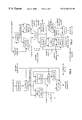
- FIG. 1 illustrates a schematic block diagram of a processing unit in accordance with the present invention
- FIG. 2 illustrates a schematic block diagram of a configurable arithmetic logic unit (ALU) module in accordance with the present invention
- FIG. 3 illustrates a schematic block diagram of another configurable ALU module in accordance with the present invention.
- FIG. 4 illustrates yet another configurable ALU module in accordance with the present invention
- FIG. 5 illustrates a schematic block diagram of a configurable ALU module in accordance with the present invention.
- FIG. 6 illustrates a logic diagram of a method for configurable processing in accordance with the present invention.
- a configurable processing unit includes a fetch module, a decoder, and a dynamic arithmetic unit.
- the fetch module is operable to fetch at least one instruction and provide it to the decoder.
- the decoder receives the instruction and decodes it.
- the dynamic arithmetic logic unit receives the decoded instruction and configures at least one configurable arithmetic logic unit to perform an operation contained within the decoded instruction.
- a processing unit may be fabricated using considerably less components than in previous processing units thereby reducing the die size and the associated costs. Further, by reducing the die size, the configurable processing unit may be included within an integrated computing system.
- FIG. 1 illustrates a schematic block diagram of a configurable processor 10 that includes an instruction cache 12 , a fetch module 14 , a decoder 16 , and a dynamic arithmetic unit 18 .
- the instruction cache 12 , fetch module 14 , and decoder 16 which may further include instruction issuance functionality, may be of conventional design.
- the instruction cache 12 stores instructions 22 which are fetched, via the fetch module 14 , and provided to the decoder 16 .
- the decoder decodes the instruction to produce a decoded instruction 24 .
- the decoded instruction may be in accordance with x 86 microcode instructions.
- the dynamic arithmetic unit 18 includes at least one configurable arithmetic unit 20 .
- the configurable arithmetic unit 20 Upon receiving the decoded instruction 24 , the configurable arithmetic unit 20 is configured to perform the appropriate operation indicated in the decoded instruction 24 . Once configured, the configurable arithmetic unit 20 performs the operation to produce a performed operation 26 .
- the dynamic arithmetic unit 18 may include a plurality of configurable arithmetic units similar to those shown in FIGS. 2, 3 and 4 , or may contain a single arithmetic logic unit as shown in FIG. 5 .
- FIG. 2 illustrates a schematic block diagram of a first configurable arithmetic logic unit 30 .
- the first configurable arithmetic logic unit 30 is configurable to perform an address calculation, an integer addition, an integer subtraction, an integer logic function (e.g., and, or, exclusive, compare, etc.) a packed integer addition, a packed integer subtraction and/or a packed integer logic function.
- the first configurable ALU 30 includes at least one register 32 , a formatting module 34 , an address calculation module 36 , an arithmetic/logic module 38 , a multiplexor 40 , register 42 , and multiplexor 44 .
- the register 32 is operably coupled to receive incoming data 46 , which is provided to the formatting module 34 .
- the formatting module 34 produces formatted data 35 .
- the formatted data 35 will be in accordance with the type of operation being performed. For example, if an integer function is being performed, the formatted data will be integer form. In furtherance of the example, if the data cache line is 64 bits and the integer value is 16 bits, the formatted data will have the integer values in the least significant 16 bits with the remaining bits being don't care bits. Conversely, when the decoded instruction is for a packed operation (i.e., a multi-media function), the formatted data 35 will include the packed data.
- the packed data may include a plurality of 8 bit data elements, 16 bit data elements, 32 bit data elements, or 64 bit data elements.
- the number of data elements in a formatted data 35 will depend on the bandwidth, or data cache line, of the system and the size of the data elements. For example, a 256 bit cache line will accommodate four 64 bit packed data elements.
- the incoming addressing data 46 may or may not be formatted depending on instructions in the decoded instruction 24 .
- the address calculation module 36 is operably coupled to receive the formatted data 35 and the decoded instruction 24 . If the decoded instruction 24 is for a load/store operation and/or an address calculation, the address calculation module 36 will be enabled. Once enabled, the address calculation module 36 will process the formatted data 35 to produce an address 37 . Such an address calculation is known. The address 37 will be provided as an output or to multiplexor 44 which will select address 37 based on the decoded instruction 24 to produce the performed operation 26 . If the decoded instruction is an arithmetic function or logic function, the arithmetic logic module 38 will be enabled.
- the arithmetic/logic module 38 will perform the corresponding arithmetic function or logic function upon the formatted data 35 , which will be provided to multiplexor 40 and/or multiplexor 44 .
- the multiplexor 40 based on the decoded instruction 24 , may output the arithmetic/logic result 39 to register 42 as intermediate data. If the result is provided to register 42 , the arithmetic logic module 38 performs another arithmetic and/or logic function upon the data to produce a final result as the performed operation 26 .
- the address calculation, the integer arithmetic/logic function, and multimedia arithmetic/logic function may be performed in a first pipeline interval. As such, it takes one pipeline interval for the first configurable arithmetic logic unit 30 to produce the performed operation 26 from the incoming data 46 . If the operation is a load/store function, the corresponding data will be cached in a second pipeline interval.
- the arithmetic/logic module 38 includes logic circuitry to perform the corresponding logic functions and further includes an addition module to perform the addition and/or subtraction function. Further note that the arithmetic/logic unit 38 , based on the decoded instruction 24 configures itself to process integer data or packed integer data.
- the arithmetic/logic module 38 would include eight 8 bit arithmetic/logic functional modules.
- the 8 function modules may be configured to perform separate operations, as would be the case for processing 8 bit packed data elements, or linked to provide carryover bits to process 64 bit data.
- any one of the modules of FIG. 2 could be configured to directly receive the incoming data 46 and to directly produce the performed operation 26 .
- FIG. 3 illustrates a schematic block diagram of a second configurable ALU 50 .
- the second configurable ALU 50 can be configured to perform a floating point addition, a floating point subtraction, a second integer addition, an integer subtraction, an integer logic function, a packed integer addition, a packed integer subtraction, a packed integer logic function, an integer division, an integer shift, and/or a packed integer shift.
- the second configurable ALU 50 includes an exponent module 52 , a formatting module 54 , an alignment shifter 56 , a subtraction module 58 , a multiplexor 60 , a rounding module 62 , a zero count module 64 , an addition module 66 , a normalizing shifter 68 , a rounding selection module 70 , and a multiplexor 72 .
- the formatting module 54 receives the incoming data 46 to produce formatted data 35 based on an exponent indication received by the exponent module 52 .
- the exponent module 52 receives the incoming data 46 and produces the exponent indication.
- the formatting module 54 produces, using conventional techniques, the formatting data 35 to be integer data, floating point data, packed integer data, or packed floating point data based, at least in part, on the exponent value of the incoming data.
- the alignment shifter 56 , the rounding module 62 , the addition module 66 , and the rounding selection module 70 are enabled via the decoded instruction 24 .
- the alignment shifter 56 shifts the formatted data 35 based on the exponent indication received by the exponent module 52 .
- alignment is known in the art.
- Multiplexor 60 selects, based on the decoded instruction 24 , the aligned data 53 and provides it to the rounding module 62 . Note that the generation of the alignment data 53 is performed in a first stage of a pipelined process.
- the rounding module 62 determines whether the floating point addition result 65 is to be rounded up in magnitude or not. Such a determination is made based on the decoded instruction 24 and the result.
- the rounding module 62 produces a corresponding rounding signal 57 .
- the production of the rounding signal 57 is performed in a second stage of the pipeline process.
- the addition module 66 receives the aligned data 53 from multiplexor 60 and produces two results. The first being a rounded addition result 61 , the second being an addition result 63 , which is a truncated version of the result. Both the rounded addition result 61 and addition result 63 are provided to the rounding selection module 70 . Based on the rounding signal 57 , the rounding selection module 70 selects one of the signals 61 or 63 to produce the floating point addition result 65 . The multiplexor 72 selects, based on the decoded instruction, the floating point addition result 65 as the performed operation 26 .
- subtraction module 58 To perform a floating point subtraction where the exponent difference between the incoming sources is equal to or less than one, subtraction module 58 , zero count module 64 , and normalizing shifter 68 are enabled via the decoded instruction 24 .
- the subtraction module 58 receives the formatted data 35 and produces therefrom a subtraction result 55 .
- the subtraction result 55 is selected by multiplexor 60 based on the decoded instructions 24 . Note that the production of the subtraction result 55 is done in a first stage of a pipeline process.
- the zero count module 64 receives the subtraction result 55 and produces a zero count value 59 therefrom. As is known, the zero count module 64 determines the number of zeros in the subtraction result 55 proceeding the first one (for binary values).
- the normalizing shifter 68 receives the subtraction result 55 and shifts it based on the zero count value 59 . This produces a normalized subtraction result 67 , which is selected by multiplexor 72 as the performed operation 26 .
- the second configurable arithmetic logic unit 50 may include a plurality of registers (not shown) such that data may be inputted in various locations within the ALU 50 .
- the formatted data 35 could be directly routed to, or the operands could be directly routed to, the addition module 66 without aligning.
- an integer addition operation may be performed in a single pipeline stage.
- an integer subtraction could be processed within a single pipeline stage by either the subtraction module 58 or the addition module 66 .
- To perform a shift right operation data can be directly provided to the alignment shifter 56 to produce a shifted result. The shifted result is then directly provided to multiplexor 72 , which selects it as the performed operation 26 .
- the normalizing shifter 68 which typically performs a shift left operation, can receive the formatted data 35 , or the incoming data 46 , and produce shifted data as the performed operation 26 . Also, the shifter 68 may perform a shift right operation on the data to produce the performed operation 26 . As such, by interpreting the decoded instructions, and providing the formatted data to the appropriate elements within ALU 50 , the configurable ALU 50 can perform a plurality of operations with minimal amount of circuitry. As one of average skill in the art will appreciate, any one of the modules of FIG. 3 could be configured to directly receive the incoming data 46 and to directly produce the performed operation 26 .
- FIG. 4 illustrates a schematic block diagram of a third configurable ALU 80 .
- the third configurable ALU 80 is capable of performing a floating point multiplication, an integer multiplication, a packed integer multiplication, an integer addition, an integer subtraction, an integer logic function, a packed integer addition, a packed integer subtraction and/or a packed logic function.
- the third ALU 80 includes a formatting module 82 , a multiplier tree 84 , an addition module 92 , a rounding module 94 , and a rounding selection module 96 .
- the multiplier tree 84 includes a booth decoder 86 , a partial product module 88 , and a Wallace tree module 90 .
- the multiplier tree 84 receives formatted data 35 via the booth decoder 86 and the partial product module 88 .
- the booth decoder 86 provides decodes the formatted data 35 and provides the decoded data to the partial product module 88 .
- the partial product module 88 processes, as is known, the decoded data and the formatted data to produce a partial product result.
- the Wallace tree module 90 receives the partial product result to produce first and second values 98 in a known manner. This is done in a first pipeline stage of a floating point pipelined operation.
- the rounding module 94 receives the first and second data values 98 and determines a rounding signal 104 . In essence, the rounding module 94 performs a similar function as the rounding module 62 of FIG. 3 .
- the addition module 92 adds the first and second values 98 together.
- the addition module 92 produces a truncated multiplication result 100 and a rounded multiplication result 102 .
- the rounding selection module 96 based on the rounding signal 104 selects result 100 or result 102 as the floating point multiplication result 106 .
- additional registers may be incorporated. Accordingly, by providing data directly to the addition module 92 , integer addition and subtraction may be performed. Similarly, the addition module 92 , could be configured to perform packed addition and/or subtraction. To perform packed integer logic functions or integer logic functions, the third configurable ALU would include an arithmetic/logic unit similar to the unit 38 of FIG. 2 .
- FIG. 5 illustrates a schematic block diagram of a configurable ALU 110 that is capable of performing all, or a portion, of the functions of the first configurable ALU 30 , the second configurable ALU 50 , and the third configurable ALU 80 .
- the configurable ALU 110 of FIG. 5 is a combination of the first, second, and third configurable ALUs wherein like components are shared.
- the configurable ALU 110 includes a formatting module 112 , an exponent module 114 , a right-shift register 116 , a multiplier tree 118 , a subtraction module 120 , a plurality of registers 122 , 124 , and 126 , a multiplexor 128 , a configuration control module 130 , a zero count module 132 , an addition module 136 , a rounding module 134 , a rounding selection module 138 , a left-shifter 140 , a multiplexor 142 , and a logic module 144 .
- the configuration control module 130 is operably coupled to receive the decoded instruction 24 and to produce a plurality of control signals 146 .
- control signals enable the appropriate modules such that the configurable ALU 11 O can perform floating point additions, floating point subtractions, floating point multiplications, integer additions, integer subtractions, integer multiplications, integer logic functions, and/or packed integer additions, subtractions, multiplications, and logic functions.
- multiplier tree 118 For a floating point multiplication, multiplier tree 118 would be enabled, the multiplexor 128 would select the data stored in register 24 and provide it to the addition module 136 and the rounding module 134 .
- the rounding selection module 138 would select the floating point result, which is outputted by multiplexor 132 .
- the control signals 146 would enable the addition module 136 to receive the formatted data 35 via multiplexor 128 .
- the addition module would perform its function to produce the addition result.
- the subtraction module 120 To perform an integer subtraction, the subtraction module 120 would produce a subtraction result which is stored in register 126 .
- multiplexor 128 based on control signals, would retrieve the subtraction result from register 126 and provide it directly to multiplexor 142 , which outputs the subtraction result as the performed operation 126 .
- the configurable ALU 110 can perform a plurality of integer, multimedia and floating point operations with a minimal amount of circuitry.
- the integrated real estate required to fabricate an arithmetic logic unit within a processor is minimized.
- the processing unit of the present invention may be incorporated in an integrated computing system that can be economically produced.
- FIG. 6 illustrates a logic diagram for configurable processing.
- the process begins at step 150 where an instruction is fetched.
- the process then process to step 152 where the instruction is decoded to produce a decoded instruction.
- the process then proceeds to step 154 where the decoded instruction is interpreted to identify an operation to be performed.
- the process then proceeds to step 156 where control signals are generated to configure functional modules (e.g., the ones shown in FIGS. 2 through 5 ), to perform the corresponding operation.
- functional modules e.g., the ones shown in FIGS. 2 through 5
Abstract
Description
Claims (7)
Priority Applications (1)
| Application Number | Priority Date | Filing Date | Title |
|---|---|---|---|
| US09/376,830 US6745318B1 (en) | 1999-08-18 | 1999-08-18 | Method and apparatus of configurable processing |
Applications Claiming Priority (1)
| Application Number | Priority Date | Filing Date | Title |
|---|---|---|---|
| US09/376,830 US6745318B1 (en) | 1999-08-18 | 1999-08-18 | Method and apparatus of configurable processing |
Publications (1)
| Publication Number | Publication Date |
|---|---|
| US6745318B1 true US6745318B1 (en) | 2004-06-01 |
Family
ID=32326155
Family Applications (1)
| Application Number | Title | Priority Date | Filing Date |
|---|---|---|---|
| US09/376,830 Expired - Lifetime US6745318B1 (en) | 1999-08-18 | 1999-08-18 | Method and apparatus of configurable processing |
Country Status (1)
| Country | Link |
|---|---|
| US (1) | US6745318B1 (en) |
Cited By (9)
| Publication number | Priority date | Publication date | Assignee | Title |
|---|---|---|---|---|
| US20060206696A1 (en) * | 2005-03-14 | 2006-09-14 | Fujitsu Limited | Reconfigurable processor |
| US20070038971A1 (en) * | 2003-09-30 | 2007-02-15 | Tatsuo Hiramatsu | Processing device with reconfigurable circuit, integrated circuit device and processing method using these devices |
| US20070220236A1 (en) * | 2006-03-17 | 2007-09-20 | Fujitsu Limited | Reconfigurable computing device |
| US7389403B1 (en) | 2005-08-10 | 2008-06-17 | Sun Microsystems, Inc. | Adaptive computing ensemble microprocessor architecture |
| US20090222506A1 (en) * | 2008-02-29 | 2009-09-03 | Evident Software, Inc. | System and method for metering and analyzing usage and performance data of a virtualized compute and network infrastructure |
| US7797512B1 (en) | 2007-07-23 | 2010-09-14 | Oracle America, Inc. | Virtual core management |
| US7802073B1 (en) | 2006-03-29 | 2010-09-21 | Oracle America, Inc. | Virtual core management |
| CN103562854A (en) * | 2011-04-01 | 2014-02-05 | 英特尔公司 | System, apparatus, and method for aligning registers |
| US20220374236A1 (en) * | 2021-05-20 | 2022-11-24 | Huawei Technologies Co., Ltd. | Method and system for optimizing address calculations |
Citations (10)
| Publication number | Priority date | Publication date | Assignee | Title |
|---|---|---|---|---|
| US4617625A (en) * | 1981-12-28 | 1986-10-14 | Hitachi, Ltd. | Vector processor |
| US4761755A (en) * | 1984-07-11 | 1988-08-02 | Prime Computer, Inc. | Data processing system and method having an improved arithmetic unit |
| US4866652A (en) * | 1987-09-01 | 1989-09-12 | Weitek Corporation | Floating point unit using combined multiply and ALU functions |
| US4916651A (en) * | 1988-01-29 | 1990-04-10 | Texas Instruments Incorporated | Floating point processor architecture |
| US6151682A (en) * | 1997-09-08 | 2000-11-21 | Sarnoff Corporation | Digital signal processing circuitry having integrated timing information |
| US6209078B1 (en) * | 1999-03-25 | 2001-03-27 | Lsi Logic Corporation | Accelerated multimedia processor |
| US6223198B1 (en) * | 1998-08-14 | 2001-04-24 | Advanced Micro Devices, Inc. | Method and apparatus for multi-function arithmetic |
| US6226735B1 (en) * | 1998-05-08 | 2001-05-01 | Broadcom | Method and apparatus for configuring arbitrary sized data paths comprising multiple context processing elements |
| US6249856B1 (en) * | 1991-07-08 | 2001-06-19 | Seiko Epson Corporation | RISC microprocessor architecture implementing multiple typed register sets |
| US6266760B1 (en) * | 1996-04-11 | 2001-07-24 | Massachusetts Institute Of Technology | Intermediate-grain reconfigurable processing device |
-
1999
- 1999-08-18 US US09/376,830 patent/US6745318B1/en not_active Expired - Lifetime
Patent Citations (10)
| Publication number | Priority date | Publication date | Assignee | Title |
|---|---|---|---|---|
| US4617625A (en) * | 1981-12-28 | 1986-10-14 | Hitachi, Ltd. | Vector processor |
| US4761755A (en) * | 1984-07-11 | 1988-08-02 | Prime Computer, Inc. | Data processing system and method having an improved arithmetic unit |
| US4866652A (en) * | 1987-09-01 | 1989-09-12 | Weitek Corporation | Floating point unit using combined multiply and ALU functions |
| US4916651A (en) * | 1988-01-29 | 1990-04-10 | Texas Instruments Incorporated | Floating point processor architecture |
| US6249856B1 (en) * | 1991-07-08 | 2001-06-19 | Seiko Epson Corporation | RISC microprocessor architecture implementing multiple typed register sets |
| US6266760B1 (en) * | 1996-04-11 | 2001-07-24 | Massachusetts Institute Of Technology | Intermediate-grain reconfigurable processing device |
| US6151682A (en) * | 1997-09-08 | 2000-11-21 | Sarnoff Corporation | Digital signal processing circuitry having integrated timing information |
| US6226735B1 (en) * | 1998-05-08 | 2001-05-01 | Broadcom | Method and apparatus for configuring arbitrary sized data paths comprising multiple context processing elements |
| US6223198B1 (en) * | 1998-08-14 | 2001-04-24 | Advanced Micro Devices, Inc. | Method and apparatus for multi-function arithmetic |
| US6209078B1 (en) * | 1999-03-25 | 2001-03-27 | Lsi Logic Corporation | Accelerated multimedia processor |
Cited By (18)
| Publication number | Priority date | Publication date | Assignee | Title |
|---|---|---|---|---|
| US20070038971A1 (en) * | 2003-09-30 | 2007-02-15 | Tatsuo Hiramatsu | Processing device with reconfigurable circuit, integrated circuit device and processing method using these devices |
| US7743236B2 (en) | 2005-03-14 | 2010-06-22 | Fujitsu Limited | Reconfigurable processor |
| EP1703414A1 (en) * | 2005-03-14 | 2006-09-20 | Fujitsu Limited | Reconfigurable processor with a shared functional unit |
| JP2006252440A (en) * | 2005-03-14 | 2006-09-21 | Fujitsu Ltd | Reconfigurable arithmetic processing unit |
| US20060206696A1 (en) * | 2005-03-14 | 2006-09-14 | Fujitsu Limited | Reconfigurable processor |
| JP4527571B2 (en) * | 2005-03-14 | 2010-08-18 | 富士通株式会社 | Reconfigurable processing unit |
| US7389403B1 (en) | 2005-08-10 | 2008-06-17 | Sun Microsystems, Inc. | Adaptive computing ensemble microprocessor architecture |
| US20070220236A1 (en) * | 2006-03-17 | 2007-09-20 | Fujitsu Limited | Reconfigurable computing device |
| US7802073B1 (en) | 2006-03-29 | 2010-09-21 | Oracle America, Inc. | Virtual core management |
| US8543843B1 (en) | 2006-03-29 | 2013-09-24 | Sun Microsystems, Inc. | Virtual core management |
| US7797512B1 (en) | 2007-07-23 | 2010-09-14 | Oracle America, Inc. | Virtual core management |
| US8219788B1 (en) | 2007-07-23 | 2012-07-10 | Oracle America, Inc. | Virtual core management |
| US8225315B1 (en) | 2007-07-23 | 2012-07-17 | Oracle America, Inc. | Virtual core management |
| US8281308B1 (en) | 2007-07-23 | 2012-10-02 | Oracle America, Inc. | Virtual core remapping based on temperature |
| US20090222506A1 (en) * | 2008-02-29 | 2009-09-03 | Evident Software, Inc. | System and method for metering and analyzing usage and performance data of a virtualized compute and network infrastructure |
| CN103562854A (en) * | 2011-04-01 | 2014-02-05 | 英特尔公司 | System, apparatus, and method for aligning registers |
| CN103562854B (en) * | 2011-04-01 | 2017-07-14 | 英特尔公司 | Systems, devices and methods for the register that aligns |
| US20220374236A1 (en) * | 2021-05-20 | 2022-11-24 | Huawei Technologies Co., Ltd. | Method and system for optimizing address calculations |
Similar Documents
| Publication | Publication Date | Title |
|---|---|---|
| US6377970B1 (en) | Method and apparatus for computing a sum of packed data elements using SIMD multiply circuitry | |
| JP3573755B2 (en) | Image processing processor | |
| US6009451A (en) | Method for generating barrel shifter result flags directly from input data | |
| US5991785A (en) | Determining an extremum value and its index in an array using a dual-accumulation processor | |
| EP0754998B1 (en) | An arithmetic unit | |
| US6292886B1 (en) | Scalar hardware for performing SIMD operations | |
| US6243803B1 (en) | Method and apparatus for computing a packed absolute differences with plurality of sign bits using SIMD add circuitry | |
| US6078941A (en) | Computational structure having multiple stages wherein each stage includes a pair of adders and a multiplexing circuit capable of operating in parallel | |
| US6092094A (en) | Execute unit configured to selectably interpret an operand as multiple operands or as a single operand | |
| US6401194B1 (en) | Execution unit for processing a data stream independently and in parallel | |
| EP0755015B1 (en) | Combining data values | |
| US20090249039A1 (en) | Providing Extended Precision in SIMD Vector Arithmetic Operations | |
| US6754809B1 (en) | Data processing apparatus with indirect register file access | |
| US6115729A (en) | Floating point multiply-accumulate unit | |
| US4866652A (en) | Floating point unit using combined multiply and ALU functions | |
| US7519646B2 (en) | Reconfigurable SIMD vector processing system | |
| US6446193B1 (en) | Method and apparatus for single cycle processing of data associated with separate accumulators in a dual multiply-accumulate architecture | |
| US6745318B1 (en) | Method and apparatus of configurable processing | |
| US6038675A (en) | Data processing circuit | |
| JPH11504744A (en) | System for performing arithmetic operations in single or double precision | |
| US6026486A (en) | General purpose processor having a variable bitwidth | |
| US5958000A (en) | Two-bit booth multiplier with reduced data path width | |
| US10705840B2 (en) | Apparatuses for integrating arithmetic with logic operations | |
| US6499046B1 (en) | Saturation detection apparatus and method therefor | |
| US6209012B1 (en) | System and method using mode bits to support multiple coding standards |
Legal Events
| Date | Code | Title | Description |
|---|---|---|---|
| STCF | Information on status: patent grant |
Free format text: PATENTED CASE |
|
| FPAY | Fee payment |
Year of fee payment: 4 |
|
| AS | Assignment |
Owner name: ATI INTERNATIONAL SRL, BARBADOS Free format text: ASSIGNMENT OF ASSIGNORS INTEREST;ASSIGNORS:MANSINGH, SANJAY;PATKAR, NITEEN;VAN DYKE, KORBIN;AND OTHERS;REEL/FRAME:023373/0284;SIGNING DATES FROM 19990708 TO 19990811 |
|
| AS | Assignment |
Owner name: ATI TECHNOLOGIES ULC, CANADA Free format text: ASSIGNMENT OF ASSIGNORS INTEREST;ASSIGNOR:ATI INTERNATIONAL SRL;REEL/FRAME:023574/0593 Effective date: 20091118 Owner name: ATI TECHNOLOGIES ULC,CANADA Free format text: ASSIGNMENT OF ASSIGNORS INTEREST;ASSIGNOR:ATI INTERNATIONAL SRL;REEL/FRAME:023574/0593 Effective date: 20091118 |
|
| FPAY | Fee payment |
Year of fee payment: 8 |
|
| AS | Assignment |
Owner name: ADVANCED SILICON TECHNOLOGIES, LLC, NEW HAMPSHIRE Free format text: ASSIGNMENT OF ASSIGNORS INTEREST;ASSIGNOR:ATI TECHNOLOGIES ULC;REEL/FRAME:036703/0421 Effective date: 20150925 |
|
| FPAY | Fee payment |
Year of fee payment: 12 |