US6731749B1 - Telephone line interface circuit with intelligent line current and voltage control - Google Patents
Telephone line interface circuit with intelligent line current and voltage control Download PDFInfo
- Publication number
- US6731749B1 US6731749B1 US09/312,412 US31241299A US6731749B1 US 6731749 B1 US6731749 B1 US 6731749B1 US 31241299 A US31241299 A US 31241299A US 6731749 B1 US6731749 B1 US 6731749B1
- Authority
- US
- United States
- Prior art keywords
- voltage
- circuit
- dac
- adc
- node
- Prior art date
- Legal status (The legal status is an assumption and is not a legal conclusion. Google has not performed a legal analysis and makes no representation as to the accuracy of the status listed.)
- Expired - Lifetime
Links
- 238000000034 method Methods 0.000 claims description 26
- 230000003068 static effect Effects 0.000 claims description 8
- 239000003990 capacitor Substances 0.000 claims 2
- 101710129178 Outer plastidial membrane protein porin Proteins 0.000 description 17
- 102100037820 Voltage-dependent anion-selective channel protein 1 Human genes 0.000 description 17
- 238000010586 diagram Methods 0.000 description 9
- 230000008901 benefit Effects 0.000 description 4
- 230000007423 decrease Effects 0.000 description 4
- 230000008569 process Effects 0.000 description 3
- 230000008859 change Effects 0.000 description 2
- 230000006870 function Effects 0.000 description 2
- 238000012986 modification Methods 0.000 description 2
- 230000004048 modification Effects 0.000 description 2
- 230000004913 activation Effects 0.000 description 1
- 230000006978 adaptation Effects 0.000 description 1
- 238000001514 detection method Methods 0.000 description 1
- 238000010615 ring circuit Methods 0.000 description 1
Images


Classifications
-
- H—ELECTRICITY
- H04—ELECTRIC COMMUNICATION TECHNIQUE
- H04M—TELEPHONIC COMMUNICATION
- H04M3/00—Automatic or semi-automatic exchanges
- H04M3/005—Interface circuits for subscriber lines
Definitions
- the present invention relates generally to the field of modem circuits, and more particularly, to a telephone line interface circuit.
- V-I characteristics i.e. requirements
- DC masks are commonly defined as “DC masks.”
- various countries have different requirements as to the minimum and/or maximum levels of DC off-hook line voltage permissible for a given Tip and Ring circuit.
- the DC line current cannot exceed 6.6 volts at 20 mA.
- the DC line current cannot exceed 60 mA while the voltage can be as high as 40 volts.
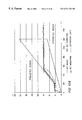
- FIGS. 10 (A)- 10 (D) The solid line on each graph represents a particular V-I boundary constraint within which the interface circuit must operate.
- the present invention provides intelligent line current and voltage control that can adjust to the various requirements of worldwide telephone systems, and/or can reduce the power consumed by the interface circuit.
- a voltage divider is connected across the rectified Tip and Ring voltage (VTR) and provides feedback of the line voltage Vtr to an electronic inductor and to an analog-to-digital converter (ADC) 10 .
- the output of the ADC 10 is then provided to a controller 30 .
- the controller 30 may be implemented as a microcontroller, using either hardware or software control.
- the controller 30 Based on the theoretical model of a telephone line network and the expected voltage/current characteristic, as dictated by the appropriate DC mask, the controller 30 sets the line current to an optimum value (via an output voltage) VDAC and causes the line voltage to adjust so as to minimize power dissipation in the circuit.
- the controller 30 can set the line current precisely via a digital-to-analog converter (DAC) 20 , by changing the voltage at the base terminal of the electronic inductor transistor Q 1 and measuring the emitter voltage Ve.
- the line current will be equal to the emitter voltage Ve divided by the emitter resistor Re.
- the controller 30 can calculate the power dissipation in the emitter resistor Re from the value of the emitter voltage Ve, and determine the power dissipation in the transistor Q 1 . While determining the optimum voltage/current line setting, the controller 30 also takes into account the specific requirements of a particular DC mask, depending upon the country of operation.
- a switch S 1 is enabled to increase the dynamic range of the ADC 10 with respect to VTR, by adding a resistor R 3 in parallel with R 2 so that a relatively large VTR can be measured within the limited voltage range of the ADC 10 (typically 0-4V).
- the ADC 10 reads the current between tip and ring (Itr) directly from the emitter of the transmitter Q 1 by measuring Ve and dividing by Re.
- the controller 30 can select either switch S 2 or S 3 to read either voltage Vtrdc or Ve.
- various feedback lines, controlled by the controller 30 are used to provide for greater current control.
- the electronic inductor transistor may also be configured as a Darlington pair. Various switches may be added to provide greater control over the operating range of the interface circuit, and are controlled by the controller 30 .
- control logic of the controller may be implemented in software, and the circuit adjusted using either a static, dynamic or static-dynamic combination control method.
- FIG. 1 is a schematic diagram of a telephone line interface circuit with DC line voltage control according to the present invention
- FIG. 2 is a schematic diagram of a telephone line interface circuit according to a second embodiment of the present invention having DC line voltage control with direct current reading;
- FIG. 3 is a schematic diagram of the equivalent DC circuit for the telephone line and modem line interface
- FIG. 4 (A) is a flow-chart of the static DC line voltage control logic according to the present invention.
- FIG. 4 (B) is a flow-chart of the dynamic DC line voltage control logic according to the present invention.
- FIG. 4 (C) is a flow-chart of an optimized DC line voltage control logic according to a preferred embodiment of the present invention.
- FIG. 5 is a schematic diagram of a telephone line interface circuit with DC line voltage control and having multiplier switches
- FIG. 6 is a schematic diagram of a telephone line interface circuit with DC line voltage control using a Darlington pair configuration
- FIG. 7 is a schematic diagram of a telephone line interface circuit with DC line voltage control using a Darlington pair configuration and having direct current reading;
- FIG. 8 is a schematic diagram of a telephone line interface circuit with DC line voltage control and having analog multiplier compensation
- FIG. 9 is a schematic diagram of a telephone line interface circuit with DC line voltage control having DAC calibration
- FIG. 10 (A) is graph of a first DC mask
- FIG. 10 (B) is graph of a second DC mask
- FIG. 10 (C) is graph of a third DC mask
- FIG. 10 (D) is graph of a fourth DC mask
- FIG. 11 is a graph of the typical operating range of a telephone line interface circuit with DC line voltage control.
- FIG. 3 is a schematic diagram of the circuit of FIG. 1 and includes the DC equivalent circuit for a telephone company central office network (CO).
- the DC characteristic of the CO can be modeled as a voltage source Vbatt, in series with a loop resistance Rloop.
- Diode bridge D 1 part of the modem telephone line interface, can be modeled as two diodes D 1 A and D 1 B, equivalent to a voltage drop of approximately 1.4V.
- Resistors R 1 and R 2 form a resistor divider with respect to voltage VTR′, and their value is chosen to be very large to make the current through them negligible compared to the current through Q 1 . Therefore, the current through Q 1 is equal to the line current Itr.
- An operational amplifier U 1 converts the voltage Vtrdc to the current required to drive the base of the transistor Q 1 , and the negative input of U 1 is connected to Ve, the emitter voltage of Q 1 , effectively making the voltage at node Vtrdc equal to Ve (virtual ground property of operational amplifiers). Since the base current of Q 1 is negligible compared to the line current ITR, the value of ITR can be calculated as Ve (voltage across Re) divided by the value of Re. In this configuration, the transistor/operational amplifier configuration operates as a voltage-controlled current source (VCCS).
- VCCS voltage-controlled current source
- An analog-to-digital converter (ADC) 10 reads the voltage at Vtrdc, and based on this reading the controller 30 determines the voltage at Tip and Ring, VTR, according to the following equations:
- VTR VTR ′+1.4V
- VTR ′ ( R 1 / R 2 ) ⁇ ( Vtrdc ⁇ VDAC )+ Vtrdc , and therefore
- VTR ( R 1 / R 2 ) ⁇ ( Vtrdc ⁇ VDAC )+ Vtrdc+ 1.4V [1]
- the factor (R 1 /R 2 ) is herein referred to as the electronic inductor “multiplier.” If switch S 1 is enabled, the value of R 2 is substituted with the parallel combination of R 2 and R 3 , or R 2 //R 3 .
- the controller 30 can also measure the line current at any point in time by using the ADC reading according to the following equation:
- the controller 30 can monitor both the line voltage and line current at any point in time, by using the same ADC reading at node Vtrdc.
- VTR represents the battery voltage at the CO (there is no voltage drop across the loop resistance).
- VTR (on-hook) Vbatt [3]
- the controller 30 calculates both VTR and ITR based on the steady-state ADC reading, and then estimates the loop resistance Rloop according to the following equations:
- Equations [1], [2], [3], and [4] form the basis for two independent methods of controlling the line voltage as a function of the line current. Specifically, equations [1] and [2] can be used to implement “dynamic” DC voltage control, whereas equations [3] and [4] combined with [1] and [2] can be used to implement “static” DC voltage control.
- the modem goes off-hook and the controller 30 sets an arbitrary initial DAC 20 setting, which results in a known VDAC voltage and switches the modem off-hook.
- the ADC 10 measures voltage Vtrdc, and the controller 30 uses equation [1] to calculate VTR and equation [2] to calculate ITR. If the value of VTR is outside the range specified by the DC mask at the current ITR, the controller 30 increases VDAC to decrease VTR or decreases VDAC to increase VTR, respectively.
- the DAC setting can be changed one bit at a time or in larger steps first and single bits later, depending on the difference between the VTR measured and the target value, and the process continues until VTR is within a specified range of the target value.
- the controller 30 recalculates ITR, as this value changes when the DAC 20 setting changes.
- the controller 30 sets an arbitrary initial DAC setting which results in a known VDAC voltage and uses equation [3] to measure Vbatt while the modem is on-hook, immediately before going off-hook.
- the controller 30 measures voltage Vtrdc, and uses equations [1] and [2] to calculate VTR and ITR, respectively.
- equation [4] the controller then calculates Rloop. Since,
- VTR V batt ⁇ ( Vtrdc/Re ) ⁇ R loop, which solved for Vtrdc yields
- Vtrdc ( V batt ⁇ VTR ) ⁇ ( Re/R loop) [5]
- VDAC ( R 2 / R 1 )[ V batt( Re/R loop)(1 +R 1 / R 2 ) ⁇
- Equation [6] relates the value of the DAC setting VDAC to line voltage VTR, assuming that Vbatt and Rloop are known. Using equation [6], therefore, the controller 30 can calculate the DAC setting as a function of the target value for VTR.
- the target value for VTR is based on the DC mask requirements and other considerations, such as power and distortion.
- the controller 30 has stored values for the DC masks shown in FIGS. 10 (A)- 10 (D), as well as the maximum power curve 13 of the transistor Q 1 , illustrated in FIG. 11 .
- the controller 30 always calculates the power dissipation in the modem line interface as
- a final DAC 20 setting that satisfies both the DC mask and power requirements can be stored by the controller 30 in a memory register MemDAC, and used as the initial DAC value (best guess) the next time the modem goes off-hook (steps 40 - 46 ). If the modem is stationary at one location (which is the case most of the time in practical applications), using the stored previous, optimal DAC value will result in fewer iterations and a faster execution of the algorithm.
- This setting can be an arbitrary default value, or it can be the DAC 20 setting used by the modem in the previous off-hook session and stored in register MemDAC.
- the controller After going off-hook (step 48 ), the controller waits (step 50 ) for a steady-state line voltage condition, typically 100 ms, measures Vtrdc, and calculates VTR and ITR using equations [1] and [2], respectively (step 52 ). Using equation [4], the controller 30 then calculates Rloop (step 54 ). Knowing Vbatt and Rloop, it is possible to calculate an optimal operating point (VTR) within the DC mask, which minimizes distortion and power dissipation in the line interface, for example (step 56 ).
- VTR optimal operating point
- an optimal value for VDAC can be calculated (step 58 ), and a corresponding value is written to the DAC (step 60 ).
- This setting is also stored in register MemDAC (step 62 ), so it can be used as initial value for the DAC the next time the modem goes off-hook. This prevents unnecessary transients when the modem goes off-hook on the same telephone line as the previous off-hook session.
- Static voltage control has the benefit of using Vbatt and Rloop to calculate the optimal operating point in the V-I domain, because all the DC circuit parameters of the loop are known. This method, however, does not use feedback from the line voltage and current to correct the possible discrepancies between calculated values and actual values.
- Discrepancies between calculated and actual line voltage values can also be caused by relative error between the ADC 10 reading and DAC 20 output voltage, for example. Relative error can be minimized by calibrating the output voltage of the DAC 20 against the ADC 10 reading, as shown in FIG. 9 . While the modem is idle, the controller 30 enables switch S 9 and reads through the ADC 10 the output of the DAC 20 for each DAC setting. A look-up table representing calibrated values of the DAC 20 vs. the ADC 10 can be stored in a memory and used by the controller 30 when selecting an appropriate value for the DAC 20 to obtain a target VTR based on the ADC 10 reading.
- the controller 30 Immediately before going off-hook, the controller 30 writes an initial value to the DAC 20 , which results in a known voltage VDAC (step 72 ).
- This setting can be an arbitrary default value, or it can be the DAC setting used by the modem in the previous communication session and stored in register MemDAC.
- the controller After going off-hook, the controller waits for a steady-state line voltage condition, typically 100 ms (step 76 ), measures Vtrdc (step 78 ), and calculates VTR and ITR using equations [1] and [2], respectively (step 80 ). If the value of VTR is outside the range specified by the DC mask at the current ITR (step 82 ), the controller 30 increases VDAC to decrease VTR or decreases VDAC to increase VTR, respectively (step 86 ).
- a steady-state line voltage condition typically 100 ms (step 76 )
- measures Vtrdc step 78
- VTR and ITR using equations [1] and [2], respectively
- VTR is within a specified range of the target value.
- the controller 30 recalculates ITR as this value changes when the DAC 20 setting changes.
- the DAC setting can be changed one bit at a time, or starting with larger steps first and single bits later, depending on the difference between the VTR measured and the target value.
- the controller 30 calculates the power dissipation in the modem line interface by multiplying the values of VTR and ITR, and compares this value with the maximum power rating Pmax (step 84 ). Since the voltages at Re and other points in the modem circuit are known, it is possible to calculate the power dissipation in each component at any one time and compare it with their individual power rating. If the power rating is within limits, the controller 30 stores the DAC setting in register MemDAC, so it can be used as initial value for the DAC 20 the next time the modem goes off-hook. This prevents unnecessary transients when the modem goes off-hook on the same telephone line as the previous off-hook session.
- Dynamic voltage control has the benefit of using continuous feedback from the line voltage and current, whereby the controller 30 can correct the DAC 20 setting recursively until the target values are obtained. Furthermore, the algorithm can run periodically to maintain the voltage and power within the target, in case the DC loop parameters change during an off-hook session. In this method, however, the controller 30 does not use knowledge of Vbatt and Rloop and cannot optimize the values of VTR and ITR to minimize distortion and power dissipation, within the V-I domain specified by the DC mask.
- An optimal voltage control solution combines the benefits of the static and dynamic methods, and thus overcomes their disadvantages.
- this is the method used by the controller 30 .
- those skilled in the art can choose the best method for a given application.
- a flowchart of this optimal method is shown in FIG. 4 (C).
- This setting can be an arbitrary default value, or it can be the DAC setting used by the modem in the previous off-hook session and stored in a register MemDAC (steps 90 - 96 ).
- the controller After going off-hook (step 98 ), the controller waits for a steady-state line voltage condition, typically 100 ms (step 100 ), measures Vtrdc, and calculates VTR and ITR using equations [1] and [2], respectively (step 102 ). Using equation [4], the controller 30 then calculates Rloop (step 104 ). Knowing Vbatt and Rloop, it is possible to calculate an optimal operating point (VTR) within the DC mask, which minimizes distortion and power dissipation in the line interface, for example (step 106 ). Using equation [6], an optimal value for VDAC can be calculated, and a corresponding value is written to the DAC (step 110 ).
- VTR optimal operating point
- the controller 30 After a short delay, to allow for a steady-state operating condition (step 112 ), the controller 30 again measures Vtrdc (step 114 ) and calculates VTR and ITR using equations [1] and [2], respectively (step 116 ). If VTR and ITR are outside the optimal target range predicted by the expected values of Vbatt and Rloop (step 118 ), the controller 30 corrects the assumed values of Vbatt and Rloop and recalculates VDAC (step 120 ). The process continues recursively until VTR and ITR are within the optimal target in the V-I domain of the DC mask, and the power is within predicted limits (step 122 ).
- the controller 30 stores the DAC setting in register MemDAC (step 124 ), so it can be used as initial value for the DAC 20 the next time the modem goes off-hook. This prevents unnecessary transients when the modem goes off-hook on the same telephone line as the previous off-hook session.
- the controller 30 can also determine the CO battery voltage Vbatt and the loop resistance Rs while off-hook, without necessarily reading the on-hook line voltage Vtr. Since equation [4] is true for any values of Vtr and Itr, the controller can take two independent readings of Vtr and Itr at state ( 1 ) and state ( 2 ). These two states can differ from each other by a different setting of the DAC, for example, or by having switch S 1 enabled or disabled, respectively. The following system of two equations in two unknowns, Vbatt and Rloop, can then be written:
- V batt ⁇ R loop ⁇ Itr ( 1 ) Vtr ( 1 )
- V batt ⁇ R loop ⁇ Itr ( 2 ) Vtr ( 2 ) [8]
- controller 30 can determine the values of Vbatt and Rloop.
- the only error allowed by this method is due to the absolute inaccuracy of the ADC 10 , and the tolerance of components used in the determination of VTR and ITR. These quantities can be specified within reasonable limits and result in negligible offset. Some of the quantities that can be defined based on acceptable margins of error are the resolution of the ADC 10 and DAC 20 (typically 6 to 8 bits), the DC offset of the op-amp U 1 , and the tolerance of resistors R 1 , R 2 , R 3 , and Re, typically 1% to 5% for practical applications.
- control logic of the present invention may be implemented by various means known to those skilled in the art, including either a hardware or software implementation.
- switch S 1 is enabled to increase the dynamic range of the ADC 10 with respect to VTR, by adding resistor R 3 in parallel with R so that a relatively large VTR can be measured within the limited voltage range of the ADC 10 (typically 0-4V). For example, if VTR is expected to be as high as 60V while the modem is on-hook, R 3 is chosen so that the ratio (R 2 //R 3 )/(R 1 +R 2 //R 3 ) is approximately 15 (60V/4V).
- Switch S 1 is also enabled while off-hook, typically to comply with TBR 21 specifications (Europe) whereby ITR is limited to 60 mA and VTR can be as high as 40V.
- a power curve is also drawn. This represents an upper limit on the maximum power dissipation of the transistor Q 1 and represents an upper boundary on the other sets of curves.
- FIG. 5 An alternate embodiment of the present invention is shown schematically in FIG. 5 .
- the controller 30 can control two switches, S 1 and a second switch S 4 , connected to the DAC 20 . This allows even greater control over the range of desired V-I characteristics as the values of R 3 and R 2 can be chosen to be independent of each other. Additionally, two switches S 5 and S 6 have been added to the feedback line of the op-amp U 1 . The controller 30 can select whichever switch provides the best “multiplier” factor for the resistor divider. Specifically, the values of R 2 and R 3 can be chosen to be as large as possible to minimize the multiplier factor, and the controller 30 can select either switch S 5 or S 6 to cover the operating range in the V-I domain as required.
- FIG. 6 Another embodiment of the present invention is illustrated schematically in FIG. 6 .
- the single transistor Q 1 described above has been replaced with a Darlington pair Q 2 , Q 3 .
- the Darlington pair configuration allows for larger line currents with less diode current from op-amp U 2 .
- three switches have been added to the op-amp's U 1 feedback to provide an extra “multiplier” enhancement option, as described in reference to FIG. 5 .
- the features of circuits described in FIG. 5 and 6 can be combined with the direct current reading of the circuit of FIG. 2, as shown in FIG. 7 .
- Two switches S 1 and S 4 are used to select the appropriate resistor divider network.
- Switches S 2 and S 3 are used to select either a voltage or a current reading, respectively, and switches S 5 , S 6 and S 7 control the feedback to the op-amp U 1 .
- Closing switches S 5 , S 6 , and S 7 causes the following equations to be true, respectively, regardless of the values of R 1 , R 2 , AND R 3 :
- Vtrdc Ve+Vbe ( Q 3 )+ Vbe ( Q 2 ) for S 5 , closed,
- Vtrdc Ve+Vbe ( Q 3 ) for S 6 closed
- Vtrdc Ve for S 7 closed.
- FIG. 8 shows a circuit configuration equivalent to FIG. 6, wherein switches S 6 and S 7 have been replaced by two analog feedback resistors R 4 and R 5 .
- Resistor R 4 is connected between the emitter of Q 3 and the negative feedback of U 1
- resistor R 5 is connected between the negative feedback of U 1 and an arbitrary voltage reference VREF.
- Ve is less than VREF and the ratio of R 4 /R 5 can be chosen so that Vtrdc is approximately equal to Ve+0.7V, which is equivalent to having switch S 6 closed.
- FIG. 9 The preferred embodiment is shown in FIG. 9 with the addition of a DAC calibration switch S 9 .
- the operation and scope of the circuitry of FIG. 9 has already been discussed.
Abstract
Description
Claims (36)
Priority Applications (6)
| Application Number | Priority Date | Filing Date | Title |
|---|---|---|---|
| US09/312,412 US6731749B1 (en) | 1999-05-14 | 1999-05-14 | Telephone line interface circuit with intelligent line current and voltage control |
| AT00932198T ATE246425T1 (en) | 1999-05-14 | 2000-05-09 | TELEPHONE LINE INTERFACE CIRCUIT WITH INTELLIGENT CURRENT AND VOLTAGE CONTROL |
| DE60004151T DE60004151T2 (en) | 1999-05-14 | 2000-05-09 | TELEPHONE LINE INTERFACE CIRCUIT WITH INTELLIGENT CURRENT AND VOLTAGE CONTROL |
| PCT/US2000/012595 WO2000070856A1 (en) | 1999-05-14 | 2000-05-09 | Telephone line interface circuit with intelligent line current and voltage control |
| EP00932198A EP1095497B1 (en) | 1999-05-14 | 2000-05-09 | Telephone line interface circuit with intelligent line current and voltage control |
| TW089109096A TW503640B (en) | 1999-05-14 | 2000-05-12 | Telephone line interface circuit with intelligent line current and voltage control |
Applications Claiming Priority (1)
| Application Number | Priority Date | Filing Date | Title |
|---|---|---|---|
| US09/312,412 US6731749B1 (en) | 1999-05-14 | 1999-05-14 | Telephone line interface circuit with intelligent line current and voltage control |
Publications (1)
| Publication Number | Publication Date |
|---|---|
| US6731749B1 true US6731749B1 (en) | 2004-05-04 |
Family
ID=23211319
Family Applications (1)
| Application Number | Title | Priority Date | Filing Date |
|---|---|---|---|
| US09/312,412 Expired - Lifetime US6731749B1 (en) | 1999-05-14 | 1999-05-14 | Telephone line interface circuit with intelligent line current and voltage control |
Country Status (6)
| Country | Link |
|---|---|
| US (1) | US6731749B1 (en) |
| EP (1) | EP1095497B1 (en) |
| AT (1) | ATE246425T1 (en) |
| DE (1) | DE60004151T2 (en) |
| TW (1) | TW503640B (en) |
| WO (1) | WO2000070856A1 (en) |
Cited By (2)
| Publication number | Priority date | Publication date | Assignee | Title |
|---|---|---|---|---|
| US20030048896A1 (en) * | 2001-08-17 | 2003-03-13 | Alberto Canella | Telephone system with current regulation in the constant current region |
| US20100277301A1 (en) * | 2005-06-30 | 2010-11-04 | At&T Intellectual Property I, L.P. | Network to alarm panel simulator for voip |
Citations (22)
| Publication number | Priority date | Publication date | Assignee | Title |
|---|---|---|---|---|
| FR2403690A1 (en) | 1977-09-14 | 1979-04-13 | Labo Cent Telecommunicat | Active dipole gyrator for telephone line - uses transistor with base coupled to output of operational amplifier |
| US4359609A (en) * | 1980-06-20 | 1982-11-16 | Advanced Micro Devices, Inc. | Circuit with feedback for controlling the impedance thereof |
| US4528424A (en) | 1983-06-24 | 1985-07-09 | International Telephone And Telegraph Corporation | Multiparty line adapter with privacy feature controlled by reversal of line polarity at a central power source |
| US4607140A (en) | 1984-03-05 | 1986-08-19 | Rockwell International Corp. | Build out capacitor circuit |
| US4607141A (en) | 1984-03-05 | 1986-08-19 | Rockwell International Corporation | Active network termination circuit |
| US4993063A (en) | 1987-03-03 | 1991-02-12 | Kiko Frederick J | Channel unit interface circuit |
| US5349638A (en) | 1993-01-25 | 1994-09-20 | Micro-Technology Inc.-Wisconsin | Universal calling/originating number identification |
| US5351289A (en) | 1992-09-17 | 1994-09-27 | Logsdon William K | Caller ID telephone security device |
| US5361296A (en) | 1991-11-25 | 1994-11-01 | Zoom Telephonics, Inc. | Modem with ring detection/modem processing capability |
| US5369666A (en) | 1992-06-09 | 1994-11-29 | Rockwell International Corporation | Modem with digital isolation |
| US5473552A (en) | 1994-06-15 | 1995-12-05 | Intel Corporation | Scheme for isolating a computer system from a data transmission network |
| US5544241A (en) | 1995-06-27 | 1996-08-06 | Andrew S. Dibner | Telephone ring detector |
| US5546448A (en) | 1994-11-10 | 1996-08-13 | Multi-Tech Systems, Inc. | Apparatus and method for a caller ID modem interface |
| US5675640A (en) | 1995-05-19 | 1997-10-07 | Lucent Technologies Inc. | Telephone ringing signal detector |
| US5737397A (en) | 1992-11-06 | 1998-04-07 | Compaq Computer Corporation | Modem having separate modem engine and data access arrangement |
| US5764694A (en) | 1996-01-25 | 1998-06-09 | Rockwell International Corporation | Self-testing and evaluation system |
| US5771281A (en) | 1995-05-02 | 1998-06-23 | Batten, Jr.; George Washington | Serial-port powered caller identification computer interface |
| US5781621A (en) | 1995-03-17 | 1998-07-14 | Motorola, Inc. | Microcontroller with a caller identification unit |
| US5790656A (en) | 1995-09-29 | 1998-08-04 | Rockwell International Corporation | Data access arrangement with telephone interface |
| US5796815A (en) | 1996-12-05 | 1998-08-18 | Advanced Micro Devices, Inc. | Communications device with improved ring signal detection |
| US5799060A (en) | 1996-05-16 | 1998-08-25 | Harris Corporation | Multi-port caller ID-based telephone ringback test device |
| US5912513A (en) * | 1997-11-14 | 1999-06-15 | Lucent Technologies, Inc. | Method and apparatus for reducing power dissipation in DC termination circuit |
-
1999
- 1999-05-14 US US09/312,412 patent/US6731749B1/en not_active Expired - Lifetime
-
2000
- 2000-05-09 DE DE60004151T patent/DE60004151T2/en not_active Expired - Lifetime
- 2000-05-09 EP EP00932198A patent/EP1095497B1/en not_active Expired - Lifetime
- 2000-05-09 AT AT00932198T patent/ATE246425T1/en not_active IP Right Cessation
- 2000-05-09 WO PCT/US2000/012595 patent/WO2000070856A1/en active IP Right Grant
- 2000-05-12 TW TW089109096A patent/TW503640B/en not_active IP Right Cessation
Patent Citations (22)
| Publication number | Priority date | Publication date | Assignee | Title |
|---|---|---|---|---|
| FR2403690A1 (en) | 1977-09-14 | 1979-04-13 | Labo Cent Telecommunicat | Active dipole gyrator for telephone line - uses transistor with base coupled to output of operational amplifier |
| US4359609A (en) * | 1980-06-20 | 1982-11-16 | Advanced Micro Devices, Inc. | Circuit with feedback for controlling the impedance thereof |
| US4528424A (en) | 1983-06-24 | 1985-07-09 | International Telephone And Telegraph Corporation | Multiparty line adapter with privacy feature controlled by reversal of line polarity at a central power source |
| US4607140A (en) | 1984-03-05 | 1986-08-19 | Rockwell International Corp. | Build out capacitor circuit |
| US4607141A (en) | 1984-03-05 | 1986-08-19 | Rockwell International Corporation | Active network termination circuit |
| US4993063A (en) | 1987-03-03 | 1991-02-12 | Kiko Frederick J | Channel unit interface circuit |
| US5361296A (en) | 1991-11-25 | 1994-11-01 | Zoom Telephonics, Inc. | Modem with ring detection/modem processing capability |
| US5369666A (en) | 1992-06-09 | 1994-11-29 | Rockwell International Corporation | Modem with digital isolation |
| US5351289A (en) | 1992-09-17 | 1994-09-27 | Logsdon William K | Caller ID telephone security device |
| US5737397A (en) | 1992-11-06 | 1998-04-07 | Compaq Computer Corporation | Modem having separate modem engine and data access arrangement |
| US5349638A (en) | 1993-01-25 | 1994-09-20 | Micro-Technology Inc.-Wisconsin | Universal calling/originating number identification |
| US5473552A (en) | 1994-06-15 | 1995-12-05 | Intel Corporation | Scheme for isolating a computer system from a data transmission network |
| US5546448A (en) | 1994-11-10 | 1996-08-13 | Multi-Tech Systems, Inc. | Apparatus and method for a caller ID modem interface |
| US5781621A (en) | 1995-03-17 | 1998-07-14 | Motorola, Inc. | Microcontroller with a caller identification unit |
| US5771281A (en) | 1995-05-02 | 1998-06-23 | Batten, Jr.; George Washington | Serial-port powered caller identification computer interface |
| US5675640A (en) | 1995-05-19 | 1997-10-07 | Lucent Technologies Inc. | Telephone ringing signal detector |
| US5544241A (en) | 1995-06-27 | 1996-08-06 | Andrew S. Dibner | Telephone ring detector |
| US5790656A (en) | 1995-09-29 | 1998-08-04 | Rockwell International Corporation | Data access arrangement with telephone interface |
| US5764694A (en) | 1996-01-25 | 1998-06-09 | Rockwell International Corporation | Self-testing and evaluation system |
| US5799060A (en) | 1996-05-16 | 1998-08-25 | Harris Corporation | Multi-port caller ID-based telephone ringback test device |
| US5796815A (en) | 1996-12-05 | 1998-08-18 | Advanced Micro Devices, Inc. | Communications device with improved ring signal detection |
| US5912513A (en) * | 1997-11-14 | 1999-06-15 | Lucent Technologies, Inc. | Method and apparatus for reducing power dissipation in DC termination circuit |
Non-Patent Citations (2)
| Title |
|---|
| The LM3900: A New Current Differencing quad of +/- Input Amplifiers, National Semiconductor Application Note 72, Sep. 1972, p. 35. * |
| The LM3900: A New Current Differencing quad of +/− Input Amplifiers, National Semiconductor Application Note 72, Sep. 1972, p. 35. |
Cited By (5)
| Publication number | Priority date | Publication date | Assignee | Title |
|---|---|---|---|---|
| US20030048896A1 (en) * | 2001-08-17 | 2003-03-13 | Alberto Canella | Telephone system with current regulation in the constant current region |
| US6980648B2 (en) * | 2001-08-17 | 2005-12-27 | Infineon Technologies Ag | Telephone system with current regulation in the constant current region |
| US20100277301A1 (en) * | 2005-06-30 | 2010-11-04 | At&T Intellectual Property I, L.P. | Network to alarm panel simulator for voip |
| US8401153B2 (en) * | 2005-06-30 | 2013-03-19 | At&T Intellectual Property I, L.P. | Network to alarm panel simulator for VoIP |
| US8699671B2 (en) | 2005-06-30 | 2014-04-15 | At&T Intellectual Property I, L.P. | Network to alarm panel simulator for VoIP |
Also Published As
| Publication number | Publication date |
|---|---|
| WO2000070856A1 (en) | 2000-11-23 |
| DE60004151T2 (en) | 2004-05-27 |
| ATE246425T1 (en) | 2003-08-15 |
| TW503640B (en) | 2002-09-21 |
| EP1095497A1 (en) | 2001-05-02 |
| DE60004151D1 (en) | 2003-09-04 |
| EP1095497B1 (en) | 2003-07-30 |
Similar Documents
| Publication | Publication Date | Title |
|---|---|---|
| US5682093A (en) | Apparatus and method for reducing the power consumption of an electronic device | |
| JP5143320B2 (en) | Offset voltage cancellation system for radio frequency power controller | |
| US7813150B2 (en) | Compensation for parameter variations in a feedback circuit | |
| EP1400014B1 (en) | Power amplifier (pa) with improved power regulation | |
| KR100547236B1 (en) | Bias Stabilization Circuit in Power Amplifier | |
| JP2002232240A (en) | Temperature compensating circuit for power amplifier | |
| CN101124723A (en) | Current limiting circuit for RF power amplifier | |
| US6437647B1 (en) | Current mirror compensation system for power amplifiers | |
| JP3526267B2 (en) | Stabilized power supply circuit | |
| US6731749B1 (en) | Telephone line interface circuit with intelligent line current and voltage control | |
| US20030071688A1 (en) | Temperature compensated current mirror | |
| US7245146B2 (en) | Semiconductor device with termination resistance adjusting circuit | |
| US8073409B2 (en) | System and method for controlling transmitter output levels in a wireless communications device | |
| WO2000070856A9 (en) | Telephone line interface circuit with intelligent line current and voltage control | |
| KR20000022828A (en) | Programmable subscriber loop interface circuit and method | |
| KR100293147B1 (en) | Apparatus for error compensation as to transmittion power of mobile communication terminal | |
| KR101258281B1 (en) | Voltage to current converter and method for converting | |
| JPH0236728A (en) | Gain one current limiter | |
| JP3060607B2 (en) | Hot wire flow meter | |
| KR100539184B1 (en) | Bandgap Voltage Reference Circuit | |
| JP2789745B2 (en) | Non-linear variable temperature compensation circuit | |
| US5336987A (en) | Voltage stabilizing circuit of switching power supply circuit | |
| KR20040025393A (en) | Biac circuit for power amplifier | |
| JPS63239368A (en) | Ignition device for internal combustion engine | |
| JP2000114994A (en) | Temperature compensating device in tdma transmitter and tdma transmitter |
Legal Events
| Date | Code | Title | Description |
|---|---|---|---|
| AS | Assignment |
Owner name: CONEXANT SYSTEMS, INC., CALIFORNIA Free format text: ASSIGNMENT OF ASSIGNORS INTEREST;ASSIGNORS:SACCA, FRANK;RAHAMIM, RAPHAEL;SKOV, JAMES BUNDE VILLADSEN;AND OTHERS;REEL/FRAME:010165/0228 Effective date: 19990805 |
|
| AS | Assignment |
Owner name: CREDIT SUISSE FIRST BOSTON, NEW YORK Free format text: SECURITY INTEREST;ASSIGNOR:CONEXANT SYSTEMS, INC.;REEL/FRAME:010450/0899 Effective date: 19981221 |
|
| AS | Assignment |
Owner name: CONEXANT SYSTEMS, INC., CALIFORNIA Free format text: RELEASE OF SECURITY INTEREST;ASSIGNOR:CREDIT SUISSE FIRST BOSTON;REEL/FRAME:012252/0865 Effective date: 20011018 Owner name: BROOKTREE CORPORATION, CALIFORNIA Free format text: RELEASE OF SECURITY INTEREST;ASSIGNOR:CREDIT SUISSE FIRST BOSTON;REEL/FRAME:012252/0865 Effective date: 20011018 Owner name: BROOKTREE WORLDWIDE SALES CORPORATION, CALIFORNIA Free format text: RELEASE OF SECURITY INTEREST;ASSIGNOR:CREDIT SUISSE FIRST BOSTON;REEL/FRAME:012252/0865 Effective date: 20011018 Owner name: CONEXANT SYSTEMS WORLDWIDE, INC., CALIFORNIA Free format text: RELEASE OF SECURITY INTEREST;ASSIGNOR:CREDIT SUISSE FIRST BOSTON;REEL/FRAME:012252/0865 Effective date: 20011018 |
|
| STCF | Information on status: patent grant |
Free format text: PATENTED CASE |
|
| AS | Assignment |
Owner name: BANK OF NEW YORK TRUST COMPANY, N.A.,ILLINOIS Free format text: SECURITY AGREEMENT;ASSIGNOR:CONEXANT SYSTEMS, INC.;REEL/FRAME:018711/0818 Effective date: 20061113 Owner name: BANK OF NEW YORK TRUST COMPANY, N.A., ILLINOIS Free format text: SECURITY AGREEMENT;ASSIGNOR:CONEXANT SYSTEMS, INC.;REEL/FRAME:018711/0818 Effective date: 20061113 |
|
| FPAY | Fee payment |
Year of fee payment: 4 |
|
| REMI | Maintenance fee reminder mailed | ||
| AS | Assignment |
Owner name: CONEXANT SYSTEMS, INC.,CALIFORNIA Free format text: RELEASE BY SECURED PARTY;ASSIGNOR:THE BANK OF NEW YORK MELLON TRUST COMPANY, N.A. (FORMERLY, THE BANK OF NEW YORK TRUST COMPANY, N.A.);REEL/FRAME:023998/0838 Effective date: 20100128 Owner name: CONEXANT SYSTEMS, INC., CALIFORNIA Free format text: RELEASE BY SECURED PARTY;ASSIGNOR:THE BANK OF NEW YORK MELLON TRUST COMPANY, N.A. (FORMERLY, THE BANK OF NEW YORK TRUST COMPANY, N.A.);REEL/FRAME:023998/0838 Effective date: 20100128 |
|
| AS | Assignment |
Owner name: THE BANK OF NEW YORK, MELLON TRUST COMPANY, N.A.,I Free format text: SECURITY AGREEMENT;ASSIGNORS:CONEXANT SYSTEMS, INC.;CONEXANT SYSTEMS WORLDWIDE, INC.;CONEXANT, INC.;AND OTHERS;REEL/FRAME:024066/0075 Effective date: 20100310 Owner name: THE BANK OF NEW YORK, MELLON TRUST COMPANY, N.A., Free format text: SECURITY AGREEMENT;ASSIGNORS:CONEXANT SYSTEMS, INC.;CONEXANT SYSTEMS WORLDWIDE, INC.;CONEXANT, INC.;AND OTHERS;REEL/FRAME:024066/0075 Effective date: 20100310 |
|
| FPAY | Fee payment |
Year of fee payment: 8 |
|
| REMI | Maintenance fee reminder mailed | ||
| FPAY | Fee payment |
Year of fee payment: 12 |
|
| SULP | Surcharge for late payment |
Year of fee payment: 11 |
|
| AS | Assignment |
Owner name: CONEXANT SYSTEMS WORLDWIDE, INC., CALIFORNIA Free format text: RELEASE BY SECURED PARTY;ASSIGNOR:THE BANK OF NEW YORK MELLON TRUST COMPANY, N.A.;REEL/FRAME:038631/0452 Effective date: 20140310 Owner name: BROOKTREE BROADBAND HOLDING, INC., CALIFORNIA Free format text: RELEASE BY SECURED PARTY;ASSIGNOR:THE BANK OF NEW YORK MELLON TRUST COMPANY, N.A.;REEL/FRAME:038631/0452 Effective date: 20140310 Owner name: CONEXANT, INC., CALIFORNIA Free format text: RELEASE BY SECURED PARTY;ASSIGNOR:THE BANK OF NEW YORK MELLON TRUST COMPANY, N.A.;REEL/FRAME:038631/0452 Effective date: 20140310 Owner name: CONEXANT SYSTEMS, INC., CALIFORNIA Free format text: RELEASE BY SECURED PARTY;ASSIGNOR:THE BANK OF NEW YORK MELLON TRUST COMPANY, N.A.;REEL/FRAME:038631/0452 Effective date: 20140310 |
|
| AS | Assignment |
Owner name: LAKESTAR SEMI INC., NEW YORK Free format text: CHANGE OF NAME;ASSIGNOR:CONEXANT SYSTEMS, INC.;REEL/FRAME:038777/0885 Effective date: 20130712 |
|
| AS | Assignment |
Owner name: CONEXANT SYSTEMS, INC., CALIFORNIA Free format text: ASSIGNMENT OF ASSIGNORS INTEREST;ASSIGNOR:LAKESTAR SEMI INC.;REEL/FRAME:038803/0693 Effective date: 20130712 |
|
| AS | Assignment |
Owner name: CONEXANT SYSTEMS, LLC, CALIFORNIA Free format text: CHANGE OF NAME;ASSIGNOR:CONEXANT SYSTEMS, INC.;REEL/FRAME:042986/0613 Effective date: 20170320 |
|
| AS | Assignment |
Owner name: SYNAPTICS INCORPORATED, CALIFORNIA Free format text: ASSIGNMENT OF ASSIGNORS INTEREST;ASSIGNOR:CONEXANT SYSTEMS, LLC;REEL/FRAME:043786/0267 Effective date: 20170901 |
|
| AS | Assignment |
Owner name: WELLS FARGO BANK, NATIONAL ASSOCIATION, NORTH CAROLINA Free format text: SECURITY INTEREST;ASSIGNOR:SYNAPTICS INCORPORATED;REEL/FRAME:044037/0896 Effective date: 20170927 Owner name: WELLS FARGO BANK, NATIONAL ASSOCIATION, NORTH CARO Free format text: SECURITY INTEREST;ASSIGNOR:SYNAPTICS INCORPORATED;REEL/FRAME:044037/0896 Effective date: 20170927 |