US6709607B2 - Flexible optic connector assembly - Google Patents
Flexible optic connector assembly Download PDFInfo
- Publication number
- US6709607B2 US6709607B2 US10/136,871 US13687102A US6709607B2 US 6709607 B2 US6709607 B2 US 6709607B2 US 13687102 A US13687102 A US 13687102A US 6709607 B2 US6709607 B2 US 6709607B2
- Authority
- US
- United States
- Prior art keywords
- layer
- optical waveguide
- waveguide
- providing
- optical
- Prior art date
- Legal status (The legal status is an assumption and is not a legal conclusion. Google has not performed a legal analysis and makes no representation as to the accuracy of the status listed.)
- Expired - Fee Related
Links
- 230000003287 optical effect Effects 0.000 claims abstract description 102
- 238000000034 method Methods 0.000 claims description 46
- 239000000463 material Substances 0.000 claims description 30
- 238000005253 cladding Methods 0.000 claims description 24
- 239000000758 substrate Substances 0.000 claims description 11
- 238000000059 patterning Methods 0.000 claims description 6
- 238000000151 deposition Methods 0.000 claims description 5
- 239000010453 quartz Substances 0.000 claims description 4
- VYPSYNLAJGMNEJ-UHFFFAOYSA-N silicon dioxide Inorganic materials O=[Si]=O VYPSYNLAJGMNEJ-UHFFFAOYSA-N 0.000 claims description 4
- 239000000853 adhesive Substances 0.000 claims description 3
- 230000001070 adhesive effect Effects 0.000 claims description 3
- 238000005530 etching Methods 0.000 claims description 2
- 239000012780 transparent material Substances 0.000 claims 8
- 238000004519 manufacturing process Methods 0.000 abstract description 12
- 230000000007 visual effect Effects 0.000 abstract description 6
- 239000000835 fiber Substances 0.000 description 32
- 229920004738 ULTEM® Polymers 0.000 description 15
- 238000013459 approach Methods 0.000 description 14
- 239000011162 core material Substances 0.000 description 10
- 230000008878 coupling Effects 0.000 description 9
- 238000010168 coupling process Methods 0.000 description 9
- 238000005859 coupling reaction Methods 0.000 description 9
- 239000013307 optical fiber Substances 0.000 description 8
- 229920000642 polymer Polymers 0.000 description 8
- UMIVXZPTRXBADB-UHFFFAOYSA-N benzocyclobutene Chemical compound C1=CC=C2CCC2=C1 UMIVXZPTRXBADB-UHFFFAOYSA-N 0.000 description 7
- 229910052751 metal Inorganic materials 0.000 description 6
- 239000002184 metal Substances 0.000 description 6
- 230000005693 optoelectronics Effects 0.000 description 6
- 239000004593 Epoxy Substances 0.000 description 4
- XUIMIQQOPSSXEZ-UHFFFAOYSA-N Silicon Chemical compound [Si] XUIMIQQOPSSXEZ-UHFFFAOYSA-N 0.000 description 4
- 229910052710 silicon Inorganic materials 0.000 description 4
- 239000010703 silicon Substances 0.000 description 4
- 238000005516 engineering process Methods 0.000 description 2
- 229920005570 flexible polymer Polymers 0.000 description 2
- PCHJSUWPFVWCPO-UHFFFAOYSA-N gold Chemical compound [Au] PCHJSUWPFVWCPO-UHFFFAOYSA-N 0.000 description 2
- 229910052737 gold Inorganic materials 0.000 description 2
- 239000010931 gold Substances 0.000 description 2
- 230000013011 mating Effects 0.000 description 2
- 238000004806 packaging method and process Methods 0.000 description 2
- 229920002120 photoresistant polymer Polymers 0.000 description 2
- 239000000126 substance Substances 0.000 description 2
- 239000004697 Polyetherimide Substances 0.000 description 1
- 230000006978 adaptation Effects 0.000 description 1
- 229910052782 aluminium Inorganic materials 0.000 description 1
- XAGFODPZIPBFFR-UHFFFAOYSA-N aluminium Chemical compound [Al] XAGFODPZIPBFFR-UHFFFAOYSA-N 0.000 description 1
- 230000003321 amplification Effects 0.000 description 1
- 238000003491 array Methods 0.000 description 1
- 230000000712 assembly Effects 0.000 description 1
- 238000000429 assembly Methods 0.000 description 1
- 239000012298 atmosphere Substances 0.000 description 1
- 230000005540 biological transmission Effects 0.000 description 1
- 238000005266 casting Methods 0.000 description 1
- 239000003795 chemical substances by application Substances 0.000 description 1
- 239000002131 composite material Substances 0.000 description 1
- 238000005520 cutting process Methods 0.000 description 1
- 230000008021 deposition Effects 0.000 description 1
- 239000010432 diamond Substances 0.000 description 1
- 229910003460 diamond Inorganic materials 0.000 description 1
- 239000003989 dielectric material Substances 0.000 description 1
- 230000000694 effects Effects 0.000 description 1
- 238000005538 encapsulation Methods 0.000 description 1
- 239000003292 glue Substances 0.000 description 1
- ZNKMCMOJCDFGFT-UHFFFAOYSA-N gold titanium Chemical compound [Ti].[Au] ZNKMCMOJCDFGFT-UHFFFAOYSA-N 0.000 description 1
- 238000001746 injection moulding Methods 0.000 description 1
- 238000003780 insertion Methods 0.000 description 1
- 230000037431 insertion Effects 0.000 description 1
- 230000010354 integration Effects 0.000 description 1
- 239000012263 liquid product Substances 0.000 description 1
- 230000000873 masking effect Effects 0.000 description 1
- 238000001465 metallisation Methods 0.000 description 1
- 150000002739 metals Chemical class 0.000 description 1
- 238000003199 nucleic acid amplification method Methods 0.000 description 1
- 238000005498 polishing Methods 0.000 description 1
- 229920001601 polyetherimide Polymers 0.000 description 1
- 239000002861 polymer material Substances 0.000 description 1
- 230000001681 protective effect Effects 0.000 description 1
- 238000002310 reflectometry Methods 0.000 description 1
- 238000005476 soldering Methods 0.000 description 1
- 229910001258 titanium gold Inorganic materials 0.000 description 1
Images


Classifications
-
- G—PHYSICS
- G02—OPTICS
- G02B—OPTICAL ELEMENTS, SYSTEMS OR APPARATUS
- G02B6/00—Light guides; Structural details of arrangements comprising light guides and other optical elements, e.g. couplings
- G02B6/24—Coupling light guides
- G02B6/42—Coupling light guides with opto-electronic elements
- G02B6/4201—Packages, e.g. shape, construction, internal or external details
- G02B6/4204—Packages, e.g. shape, construction, internal or external details the coupling comprising intermediate optical elements, e.g. lenses, holograms
- G02B6/4214—Packages, e.g. shape, construction, internal or external details the coupling comprising intermediate optical elements, e.g. lenses, holograms the intermediate optical element having redirecting reflective means, e.g. mirrors, prisms for deflecting the radiation from horizontal to down- or upward direction toward a device
-
- G—PHYSICS
- G02—OPTICS
- G02B—OPTICAL ELEMENTS, SYSTEMS OR APPARATUS
- G02B6/00—Light guides; Structural details of arrangements comprising light guides and other optical elements, e.g. couplings
- G02B6/24—Coupling light guides
- G02B6/26—Optical coupling means
- G02B6/262—Optical details of coupling light into, or out of, or between fibre ends, e.g. special fibre end shapes or associated optical elements
-
- G—PHYSICS
- G02—OPTICS
- G02B—OPTICAL ELEMENTS, SYSTEMS OR APPARATUS
- G02B6/00—Light guides; Structural details of arrangements comprising light guides and other optical elements, e.g. couplings
- G02B6/24—Coupling light guides
- G02B6/26—Optical coupling means
- G02B6/30—Optical coupling means for use between fibre and thin-film device
-
- G—PHYSICS
- G02—OPTICS
- G02B—OPTICAL ELEMENTS, SYSTEMS OR APPARATUS
- G02B6/00—Light guides; Structural details of arrangements comprising light guides and other optical elements, e.g. couplings
- G02B6/24—Coupling light guides
- G02B6/42—Coupling light guides with opto-electronic elements
- G02B6/4201—Packages, e.g. shape, construction, internal or external details
- G02B6/4219—Mechanical fixtures for holding or positioning the elements relative to each other in the couplings; Alignment methods for the elements, e.g. measuring or observing methods especially used therefor
- G02B6/4228—Passive alignment, i.e. without a detection of the degree of coupling or the position of the elements
- G02B6/423—Passive alignment, i.e. without a detection of the degree of coupling or the position of the elements using guiding surfaces for the alignment
-
- G—PHYSICS
- G02—OPTICS
- G02B—OPTICAL ELEMENTS, SYSTEMS OR APPARATUS
- G02B6/00—Light guides; Structural details of arrangements comprising light guides and other optical elements, e.g. couplings
- G02B6/24—Coupling light guides
- G02B6/42—Coupling light guides with opto-electronic elements
- G02B6/43—Arrangements comprising a plurality of opto-electronic elements and associated optical interconnections
Definitions
- the invention pertains to optical connection and particularly to optical connectors making use of flexible connectors. More specifically, this invention pertains to the use of self-aligned, flexible optical connectors for coupling light between an optoelectronic device and an optical fiber, waveguide, or arrays of devices, fibers, and/or waveguides and a method of manufacture thereof.
- a common problem is to simultaneously provide electrical connection to an optoelectronic device as well as optical coupling from the device to an optical fiber in a connected package.
- Previous methods of such coupling have included placing the device in a first level package, such as a TO header in an optical connector receptacle, rather than placing the device directly on the circuit board providing an electrical connection from the circuit board to the TO header by means of an electrical flex circuit. This approach involves costly and time consuming methods of manufacturing.
- the present invention has self-aligning features for waveguide self-alignment to a vertically coupled optical port such as a photodetector, VCSEL, or surface emitting LED.
- the invention also includes self-aligning or passively aligned structures for connector receptacles and backplanes. While the optical devices or optoelectronic integrated circuits are still at the wafer level, the wafer is coated and photolithographically patterned to provide the self-aligning features. Specifically, a pillar of dielectric or polymer material on the photodetector or laser wafer is fabricated in a fashion such that it fits or snaps into a recess of the waveguide thus providing a passive alignment with an accuracy of better than 5 micrometers ( ⁇ m). The added feature of this is the holding of the waveguide in place after the aligning fixtures are removed.
- the features of the present invention include a self-aligning approach for coupling a waveguide or a plurality of waveguides to a vertically coupled device or devices, which can then be mounted directly onto a circuit board with other chips, without a first level package, and for connecting the other ends of the waveguides or connectors into optical connector receptacles of a module or a backplane.
- the features of this approach include an optical waveguide or array of waveguides, that optically connect an optical device or devices at one end to a connector/connector receptacle at the other end.
- Self-aligning mechanical features provide 1 to 5 ⁇ m alignment tolerances at the optical chip, while mechanical or visual alignment marks allow accurate placement of the waveguide in the connector receptacle at the other end, allowing automatic alignment to take place with machine vision.
- FIGS. 1 a and 1 b illustrate a self-alignment mechanism between a flexible coupler and a circuit board having a vertical light port.
- FIGS. 2 a and 2 b show a plug and receptacle connection of flexible couplers.
- FIGS. 3 a and 3 b illustrate alignment grooves and ridges of a flexible-coupler-to-board connection.
- FIG. 4 shows an approach using visual alignment marks for positioning a flexible waveguide in an optical fiber connector receptacle.
- FIGS. 5 a and 5 b reveal the structure of the flexible waveguide having two forty-five degree facet ends.
- FIGS. 6 a , 6 b , 6 c , 6 d , 6 e and 6 f illustrate various connections of two flexible light waveguides/fibers.
- FIG. 7 illustrates an alternative approach for aligning the waveguide structure at the connector receptacle end.
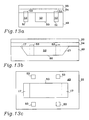
- FIGS. 8 a , 8 b , 8 c , 9 a , 9 b , 9 c , 10 a , 10 b , 10 c , 11 a , 11 b , 11 c , 12 a , 12 b , 12 c , 13 a , 13 b , 13 c , 14 a , 14 b , 14 c , 15 a , 15 b , 15 c , 16 a , 16 b , 16 c , 17 a , 17 b and 17 c illustrate a process for fabricating a passively aligned flexible optical circuit.
- FIGS. 18 a - 18 e reveal process steps for fabricating a flexible coupler having self-alignment keys.
- FIG. 19 shows the alignment of a flexible coupler secure with rigid keys.
- a polymer waveguide structure 12 (FIG. 1 a ) is used to guide light 13 to/from optical chip 14 through flexible optical circuit 12 and connector receptacle 15 and into fiber 16 which is centered with respect to connector receptacle 15 by ferrule 30 .
- Flex circuit 12 containing waveguide 20 can be constructed from a variety of materials.
- One example is an ULTEM defined waveguide circuit 12 with BCB cladding polymer layers 31 .
- a two dimensional sheet of waveguide flex circuit structures can be fabricated as will be described below, and then the individual flex circuits 12 may be separated by sawing or cutting. In the embodiment shown in FIG.
- a perpendicular cut 21 at one end is used where waveguide 12 couples to fiber 16 via connector receptacle 15 and ferrule 30 .
- a 45-degree cut 17 is made to form a turning mirror 18 to direct light out of laser 19 and into waveguide 20 , or out of waveguide 20 and into a photodetector 22 .
- the present invention adapts the self-aligning waveguide technology to enable an optical chip 14 on-board packaging approach for modules and backplanes.
- An optical chip 14 containing a light source 19 or detector 22 can be placed directly on a board 58 , with the light coupled in or out of the port 19 , 22 , through waveguide 20 , as noted in FIG. 1 b .
- this board 58 would also contain laser driver or receiver amplification I.C.s as discrete components.
- the use of a metalized 45-degree reflector 18 (in FIG. 1 a ) then allows device 12 to be covered with glob top 38 (a covering of protective dark epoxy) without affecting the optical properties.
- waveguide 20 is coupled into a connector receptacle 15 which accepts a ferrule 30 containing a fiber 16 which fits with precision inside receptacle 15 , and, as a result, is precisely aligned to waveguide 20 .
- a connector receptacle 15 holding onto both device 12 and fiber ferrule 30 .
- the same approach described here can be used to couple two waveguides together at a board to backplane interface, for instance, as shown in FIG. 2 b.
- FIG. 2 a shows the parallel waveguide flexible connector/interface 12 used to provide a rugged interface between a package or multichip module containing an optoelectronic die, and a connectorized optical fiber 16 which provides an interconnect path to the next module, board, or cabinet, via connector receptacle 23 , connector 24 and ferrule 30 .
- FIGS. 1 a and 1 b show examples of waveguide-to-chip passive mechanical alignments. Grooves 27 are etched into optical flex circuit 12 as illustrated in FIGS. 3 a and 3 b .
- a matching alignment ridge 28 is formed on the surface near laser 19 or photodetector 22 on chip 14 , by depositing and patterning an additional thick polymer layer on the surface of the chip.
- the polymer optical flex circuit contains both waveguide 20 for guiding the optical signal, and alignment wells 27 .
- Alignment ridges 28 can be photolithographically defined at the wafer level during fabrication of lasers 19 and photodetectors/receivers 22 , so that the fabrication can be very cost effective.
- Optical flex circuit 12 is multiply fabricated in large sheets, and then sawed into individual circuits 12 (with both 90-degree 21 and 45-degree 17 facets for mirrors 18 ), respectively, much as one saws up a wafer in the art.
- the fabrication of optical flex circuit 12 uses integrated circuit (IC) type manufacturing processes.
- the surface of 45-degree turning mirror 18 on optical flex circuit 12 is coated with gold or gold-titanium so that the reflectivity of turning mirror 18 is insensitive to the refractive index of the medium placed in contact with this mirror.
- Similar self-aligning structures 27 are fabricated in optical flex circuit 12 to match alignment structures 28 in connector receptacle 15 , so that flex circuit 12 is passively aligned for coupling from waveguides 20 to fibers 16 or other waveguides 20 in flex circuits 12 plugged into connector receptacle 15 , 24 or 25 . This is illustrated in FIGS. 1 a , 1 b , 2 a and 2 b.
- Optical flex circuit 12 can then be snapped onto the optical chips 14 and slid into place so 45-degree facet 17 with mirror 18 is properly located over the top of vertical port optical devices 19 and 22 on chip 14 .
- the other end 21 of the optical flex circuit 12 having slots 27 may be slotted or threaded for sliding into connector receptacle 15 having ribs 28 . This provides alignment to a fiber in a mating ferrule 30 , or to another waveguide in a mating ferrule 25 in FIG. 2 b.
- an encapsulation step can be carried out such as depositing a “glob top” or dark epoxy covering 38 (in FIG. 2 b ) over all the chips 14 . Since waveguide 12 turning mirror 18 is metalized, the use of glob top 38 provides mechanical and moisture protection for chips 14 , without affecting the coupling efficiency from optical devices 19 and 22 to optical flex circuit 12 (illustrated in more detail in FIGS. 1 a , 1 b , 3 a and 3 b ).
- the invention includes a method for packaging either a serial or parallel optoelectronic module with optical chips 14 , i.e., having laser 19 and photodetector/receiver 22 devices, mounted directly on printed circuit board 37 .
- the method is for coupling light out of the laser 19 , through a connector receptacle 24 and plug 23 and into fiber 16 , as well as from fiber 16 into the photodetector/receiver 22 .
- the flexible waveguide self-aligning interconnection also provides cost advantages by eliminating the first level package, allowing the optical chips 14 to be attached to board 37 at the same time as all the other I.C.s, and eliminating the need for an active optical alignment and soldering of a TO header with respect to the connector receptacle 24 .
- FIG. 4 shows another embodiment for the connector which provides a sleeve type connection between flex circuit 12 and fiber 16 .
- Fiber 16 is inserted with a hole 39 which may be slightly tapered with the larger diameter at the end where the fiber is inserted so as to ease the insertion of fiber 16 into hole 39 .
- the tapering of hole 39 this causes fiber 16 to enter into a tight fit in hole 39 as it approaches the other end of ferrule 30 .
- An epoxy may be applied at the end where fiber 16 enters hole 39 on ferrule 30 to secure fiber 16 to ferrule 30 .
- FIGS. 5 a and 5 b show plane and lateral views of flex circuit 12 for the embodiment having 45-degree facets for mirror 18 on both ends.
- An ULTEM waveguide is enclosed by BCB clads 31 .
- visual alignment marks 42 used for aligning mirrors 18 to other optical devices 19 or 22 , waveguides 20 , mirrors 18 or fibers 16 .
- FIGS. 6 a through 6 f connections of various combinations of flexible waveguides and/or optical fibers, having optical or mechanical alignment, are illustrated.
- a flex waveguide circuit 12 may be attached to another flex waveguide circuit 12 via receptacle 25 and sleeve 45 .
- alignment slots or keys 47 are at the ends of plug 23 and receptacle 25 . Plug 23 and receptacle 25 fit into sleeve 45 and are self-aligned with mechanical slots and keys 47 , respectively.
- FIG. 6 b shows a waveguide 12 in plug 20 which is optically connected to an optical fiber 16 in receptacle 25 .
- Waveguide 12 and fiber 16 are brought into optical alignment when plug 23 and receptacle 25 are inserted into sleeve 24 and to be proximate to each other.
- FIG. 6 c shows flex circuit 12 having waveguide 20 aligned mechanically to plate 40 via depressions 59 on circuit 20 which are mechanically aligned to pillars on plate 40 .
- Edge 61 of plate 40 is mechanically aligned with the inside diameter sleeve 45 .
- Plate 40 fits on sleeve 24 and ferrule 30 having fiber 16 , is slipped into sleeve 24 and the end of fiber 16 is optically aligned with mirror 18 which reflects light to or from waveguide 20 in flex circuit 12 .
- FIG. 6 d shows flex circuit 12 having a lens 60 .
- the depressions of circuit 12 are mechanically aligned with pillars on lens 60 .
- Lens 60 is mechanically aligned and fitted to the inside diameter of sleeve 24 .
- Ferrule 30 with fiber 16 is likewise mechanically aligned and fitted to the inside diameter of sleeve 24 , thus resulting in the optical alignment of fiber 16 with waveguide 20 of the flex circuit 12 .
- FIG. 6 e shows flex circuit 12 aligned with and attached to plate 40 like that in FIG. 6 c .
- This flex circuit 12 is optically connected to another flex circuit 12 which is similarly aligned with and attached to a plate 40 .
- the plates are attached to the respective ends of sleeve 45 whose inside diameter is mechanically aligned to edges 61 of plates 40 , respectively, resulting in optical alignment of mirrors 18 of waveguides 20 of flex circuits 12 .
- 6 f reveals a similar interconnection of flex circuits 12 except instead of mechanical alignment of pillars and depressions 59 of circuit 12 to pillars on plate 40 , there are visual alignment marks 42 which allow for either manual or machine vision alignment of flex circuit 12 to plate 40 such that when plates 40 are attached to sleeve 45 , mirrors 18 will be optically aligned with each other.
- FIG. 7 shows an interface device 15 for connecting fiber 16 to waveguide 20 of flex circuit 12 .
- Fiber 16 is fit into ferrule 30 .
- Ferrule 30 fits into receptacle 24 which is inserted into device 15 .
- the end of fiber 16 is approximately flush with the surface of device 15 which mates with the 90-degree facet 21 of circuit 12 .
- a hole 43 in device 15 and alignment marks or cross-hairs 48 on 90-degree facet 21 permit manual or machine vision alignment of the end of fiber 16 in device 15 with waveguide 20 of circuit 12 so that light can efficiently propagate between fiber 16 and waveguide 20 .
- FIG. 8 a shows a silicon die 49 for casting an ULTEM waveguide core 20 in trench-like space 50 .
- Die 49 may be made of other materials, i.e., various metals rather than silicon.
- ULTEM is a General Electric (GE) plastic-like polyetherimide which is a liquid-type of substance used for injection molding.
- GE General Electric
- Trenches 51 create raised fudicial marks when injected with ULTEM.
- FIG. 8 a is a side view which shows 45-degree folds, slants or cuts 17 in trench 50 for waveguide 20 .
- 10 a , 10 b and 10 c show the results after the removal of excess material 52 in that the new surface of material 52 in trenches 50 and 51 is even or matches up with the surfaces of die 49 .
- a mask (not shown) is formed over die 49 and material 52 to form or deposit metal on material 52 in trenches 51 and the mask for masking fudicial marks for alignment purposes or a mechanical key. The mask is then removed with just metal 53 remaining on material 52 in trenches 51 .
- a cladding layer may be formed on the “top” surfaces of die 49 , on and about metal fudicial marks 53 , and on top of ULTEM 52 of waveguide 20 .
- Cladding layer 54 is a Dow Chemical Inc. BCB (benzocyclobutene) which is a commercial liquid product that is spun on and thermally cured. Cladding 54 has a lower index of refraction than waveguide 20 and is used to confine light transmission to waveguide 20 .
- ULTEM layer 55 is formed on cladding layer 54 .
- Layer 55 is a carrier or back layer for BCB layer 54 .
- Layer 55 provides ruggedness and mechanical stability and is a handle. Layer 55 is cured at 210 degrees C.
- FIGS. 14 a , 14 b and 14 c show the fabrication of alignment keys 27 with a RIA (reactive ion agent) etchant (SF 6 ).
- Keys 27 are etched in ULTEM layer 55 and BCB layer 54 .
- Key photoresist masks (not shown) are placed over layer 55 and are aligned according to metalized fudicial marks 53 . Then keys 27 are formed via etching resulting in keys 27 aligned with marks 53 .
- FIGS. 15 a , 15 b and 15 c Quartz carrier 56 in FIGS. 15 a , 15 b and 15 c , is put on ULTEM back or carrier layer 55 via an adhesion technique. Quartz carrier 56 is already fabricated and polished before it is attached to carrier 55 .
- FIGS. 16 a and 16 b are effectively FIGS. 15 a and 15 b , flipped upside down, having silicon die 49 removed from ULTEM material 52 which formed waveguide 52 in trench 50 and material 52 formed by trenches 51 of die 49 .
- the assembly of FIGS. 15 a , 15 b and 15 c is put in a pressure cooker to effect the release of silicon master die 49 from the remaining assembly as shown in FIGS. 16 a , 16 b and 16 c.
- Metalized mirrors 18 are formed on portion of cuts or surfaces 17 .
- a metal such as gold or aluminum is formed on cuts or surfaces 17 to result in metalized fold mirrors 18 .
- a photoresist mask (not shown) is formed on the assembly of FIGS. 16 a , 16 b and 16 c , such that only the areas of surfaces 17 to be used for mirrors 18 are exposed for the ensuing deposition of the metal.
- a final BCB cladding layer 57 is formed on ULTEM material 52 , waveguide 20 , mirrors 18 and ULTEM material 52 .
- quartz carrier 56 is released and removed from ULTEM back layer 55 .
- quartz carrier 56 is released and removed from ULTEM back layer 55 .
- FIGS. 18 a - 18 e show another process sequence which may be used to produce flex circuit or flexible polymer waveguide ribbon 12 .
- a waveguide 65 layer may be deposited and photolithographically defined on a low refractive index cladding buffer layer 82 , which in turn is deposited on a flexible polymer substrate 68 .
- Wide regions of waveguide core 65 are defined adjacent to the waveguide array using a single mask level 69 in FIG. 18 a .
- Waveguides 65 are buried using a cladding polymer 29 , the same as that of layer 82 , to yield a composite waveguide system with a core refractive index higher than that of cladding 29 , and with additional buried wide regions of waveguide 65 core material in FIG. 18 b .
- a second mask level 32 is used to expose resist 33 in an area slightly wider than the wide core 65 regions. Resist 33 is exposed using a non-critical alignment step.
- a non-selective light etch e.g., O 2 +CF 4 RIE
- O 2 +CF 4 RIE e.g., O 2 +CF 4 RIE
- a selective etch O 2 RIE only
- Resulting grooves 66 are of a width defined by first level mask 69 , and thus the alignment steps are automatically aligned with respect to waveguide cores 65 located at the outside edges.
- a rigid “key” 75 having mirror image protrusions to grooves or slots 66 and possibly formed with the same mask, is fabricated using a rigid substrate and defining polymer ribs (FIG. 19 ). Key 75 may be used to align the various selections of waveguide 12 providing a complete interconnect. Key 75 is moved across surfaces 80 and 81 at the interconnect location until ribs 76 register with the grooves or slots 77 and 78 . At least one groove or slot 78 may also be fabricated from the same mask as grooves or slots 77 so as to provide alignment between waveguides 65 and 82 of less than 5 micrometers ( ⁇ m). Similarly, one or several grooves or slots may fabricated to facilitate alignment between waveguide 65 and waveguide 82 .
- Downward pressure 45 is used to align waveguide cores 65 and 82 , and insert key 75 with ribs 76 into slots 77 and 78 to interlock flex coupler 12 to board or chip 64 .
- One of a number of different adhesives can be used to cover and glue the interlocking parts together in a permanent manner.
- a second section of waveguide 65 can be aligned to a first section of waveguide 82 by sliding the two components together using key 75 to define lateral alignments 34 and 35 and vertical alignment 36 , and interlock the components in an aligned fashion.
- Self-alignment with respect to the waveguides 65 and 82 may also be obtained by the automatic positioning of two parts (a board or chip 64 and a flexible waveguide 12 ) using previously defined steps or features.
- This type of automatic positioning is an important part of a backplane approach; however, the process of defining the steps or features is still costly.
- the present invention as to a ‘self-aligning connector” uses the term “self-aligning” to describe the process by which the alignment features 66 and 78 are made in the connector components 12 and 64 using unique selective etch features of the waveguide 65 system. There is no need for any mask registration.
- the two-polymer system makes this approach possible as noted above. The impact of this idea is applicable to optical backplanes at the system level.
- the self-aligning process allows simple fabrication of the self-aligning connector assemblies 75 , 77 and 78 .
Abstract
Description
Claims (26)
Priority Applications (1)
| Application Number | Priority Date | Filing Date | Title |
|---|---|---|---|
| US10/136,871 US6709607B2 (en) | 1996-12-31 | 2002-04-30 | Flexible optic connector assembly |
Applications Claiming Priority (3)
| Application Number | Priority Date | Filing Date | Title |
|---|---|---|---|
| US77533096A | 1996-12-31 | 1996-12-31 | |
| US09/268,191 US6404960B1 (en) | 1996-12-31 | 1999-03-15 | Flexible optic connector assembly |
| US10/136,871 US6709607B2 (en) | 1996-12-31 | 2002-04-30 | Flexible optic connector assembly |
Related Parent Applications (1)
| Application Number | Title | Priority Date | Filing Date |
|---|---|---|---|
| US09/268,191 Division US6404960B1 (en) | 1996-12-31 | 1999-03-15 | Flexible optic connector assembly |
Publications (2)
| Publication Number | Publication Date |
|---|---|
| US20020181882A1 US20020181882A1 (en) | 2002-12-05 |
| US6709607B2 true US6709607B2 (en) | 2004-03-23 |
Family
ID=25104068
Family Applications (4)
| Application Number | Title | Priority Date | Filing Date |
|---|---|---|---|
| US09/135,412 Expired - Lifetime US6088498A (en) | 1996-12-31 | 1998-08-14 | Flexible optic connector assembly |
| US09/134,229 Expired - Lifetime US6069991A (en) | 1996-12-31 | 1998-08-14 | Flexible optic connector assembly |
| US09/268,191 Expired - Lifetime US6404960B1 (en) | 1996-12-31 | 1999-03-15 | Flexible optic connector assembly |
| US10/136,871 Expired - Fee Related US6709607B2 (en) | 1996-12-31 | 2002-04-30 | Flexible optic connector assembly |
Family Applications Before (3)
| Application Number | Title | Priority Date | Filing Date |
|---|---|---|---|
| US09/135,412 Expired - Lifetime US6088498A (en) | 1996-12-31 | 1998-08-14 | Flexible optic connector assembly |
| US09/134,229 Expired - Lifetime US6069991A (en) | 1996-12-31 | 1998-08-14 | Flexible optic connector assembly |
| US09/268,191 Expired - Lifetime US6404960B1 (en) | 1996-12-31 | 1999-03-15 | Flexible optic connector assembly |
Country Status (6)
| Country | Link |
|---|---|
| US (4) | US6088498A (en) |
| EP (1) | EP0950204B1 (en) |
| JP (1) | JP2001507814A (en) |
| CA (1) | CA2272751A1 (en) |
| DE (1) | DE69710098T2 (en) |
| WO (1) | WO1998029772A1 (en) |
Cited By (43)
| Publication number | Priority date | Publication date | Assignee | Title |
|---|---|---|---|---|
| US20040150092A1 (en) * | 2003-01-31 | 2004-08-05 | Morris Terrel L. | Integrated VCSELs on ASIC module using flexible electrical connections |
| US20040202214A1 (en) * | 2002-10-18 | 2004-10-14 | Aronson Lewis B. | Flexible circuit design for improved laser bias connections to optical subassemblies |
| US20050220393A1 (en) * | 2004-03-30 | 2005-10-06 | Markus Riester | Flexible active signal cable |
| US20050245118A1 (en) * | 2004-04-30 | 2005-11-03 | Finisar Corporation | Flex circuit assembly |
| US20060032665A1 (en) * | 2004-07-09 | 2006-02-16 | Ice Donald A | Single layer flex circuit |
| US20070190331A1 (en) * | 2005-02-15 | 2007-08-16 | Rpo Pty Limited | Photolithographic patterning of polymeric materials |
| US7275937B2 (en) | 2004-04-30 | 2007-10-02 | Finisar Corporation | Optoelectronic module with components mounted on a flexible circuit |
| US7311240B2 (en) | 2004-04-30 | 2007-12-25 | Finisar Corporation | Electrical circuits with button plated contacts and assembly methods |
| US20080031583A1 (en) * | 2006-08-03 | 2008-02-07 | Fuji Xerox Co., Ltd. | Flexible optical waveguide film, optical transceiver module, multi-channel optical transceiver module, and method of manufacturing flexible optical waveguide film |
| US7389015B1 (en) * | 2007-10-24 | 2008-06-17 | International Business Machines Corporation | Mechanically decoupled opto-mechanical connector for flexible optical waveguides embedded and/or attached to a printed circuit board |
| US20080159688A1 (en) * | 2006-12-31 | 2008-07-03 | Motorola Inc | Circuit substrate supporting optically and electrically conveyed signals, and method for forming same |
| US20080181561A1 (en) * | 2006-12-26 | 2008-07-31 | Hideto Furuyama | Optoelectronic interconnection board, optoelectronic interconnection apparatus, and manufacturing method thereof |
| US7439449B1 (en) | 2002-02-14 | 2008-10-21 | Finisar Corporation | Flexible circuit for establishing electrical connectivity with optical subassembly |
| US7446261B2 (en) | 2001-09-06 | 2008-11-04 | Finisar Corporation | Flexible circuit boards with tooling cutouts for optoelectronic modules |
| US20090087146A1 (en) * | 2007-09-27 | 2009-04-02 | Rolston David R | Method for assembling a two substrate parallel optical sub-assembly |
| US20090142026A1 (en) * | 2005-06-30 | 2009-06-04 | Mitsui Chemicals Inc. | Optical Waveguide Film And Photoelectric Film |
| US20090202203A1 (en) * | 2007-04-10 | 2009-08-13 | International Business Machines Corporation | Coupling Element Alignment Using Waveguide Fiducials |
| US20090232443A1 (en) * | 2005-02-28 | 2009-09-17 | Nec Corporation | Connection structure of two-dimensional array optical element and optical circuit |
| US20100129038A1 (en) * | 2008-11-21 | 2010-05-27 | Fuji Xerox Co., Ltd. | Optical transmission apparatus |
| US20100220957A1 (en) * | 2007-06-26 | 2010-09-02 | Panasonic Electric Works Co., Ltd. | Optical module |
| US20120183256A1 (en) * | 2011-01-18 | 2012-07-19 | Avago Technologies Fiber Ip (Singapore) Pte. Ltd. | Optical connection system with plug having optical turn |
| US20120189254A1 (en) * | 2011-01-26 | 2012-07-26 | Avago Technologies Fiber Ip (Singapore) Pte. Ltd. | Electrical-to-optical and optical-to-electrical converter plug |
| US8534927B1 (en) | 2012-03-23 | 2013-09-17 | International Business Machines Corporation | Flexible fiber to wafer interface |
| US20130302040A1 (en) * | 2012-05-14 | 2013-11-14 | Kuo-Fong Tseng | Optical-electrical conversion module and optical transmission assembly using the same |
| CN103777275A (en) * | 2012-10-18 | 2014-05-07 | 国际商业机器公司 | Alignment of single-mode polymer waveguide (pwg) array and silicon waveguide (siwg) array for providing adiabatic coupling |
| US20140133810A1 (en) * | 2012-10-05 | 2014-05-15 | Tyco Electronics Corporation | Flexible optical circuit, cassettes, and methods |
| US8923665B2 (en) | 2013-03-15 | 2014-12-30 | International Business Machines Corporation | Material structures for front-end of the line integration of optical polarization splitters and rotators |
| US20150247984A1 (en) * | 2014-02-28 | 2015-09-03 | Murata Manufacturing Co., Ltd. | Optical transmission module and method of manufacturing optical transmission module |
| US9146374B2 (en) | 2012-09-28 | 2015-09-29 | Adc Telecommunications, Inc. | Rapid deployment packaging for optical fiber |
| US9206965B2 (en) | 2012-12-20 | 2015-12-08 | International Business Machines Corporation | Semiconductor photonic package |
| US9268107B2 (en) | 2012-07-30 | 2016-02-23 | Hewlett Packard Enterprise Development Lp | Optical waveguide |
| US9316796B2 (en) | 2013-03-14 | 2016-04-19 | International Business Machines Corporation | Fiber pigtail with integrated lid |
| US20160109668A1 (en) * | 2014-10-17 | 2016-04-21 | Cisco Technology, Inc. | Direct printed circuit routing to stacked opto-electrical ic packages |
| US9435975B2 (en) | 2013-03-15 | 2016-09-06 | Commscope Technologies Llc | Modular high density telecommunications frame and chassis system |
| US9535229B2 (en) | 2011-10-07 | 2017-01-03 | Commscope Technologies Llc | Fiber optic cassette, system, and method |
| US9568679B2 (en) * | 2011-08-16 | 2017-02-14 | International Business Machines Corporation | Lens array optical coupling to photonic chip |
| US20170176697A1 (en) * | 2014-02-07 | 2017-06-22 | Cnam - Conservatoire National Des Arts Et Metiers | Process for manufacturing vertical optical coupling structures |
| WO2017189955A1 (en) * | 2016-04-29 | 2017-11-02 | Arizona Board Of Regents On Behalf Of The University Of Arizona | Optical printed circuit board with polymer array stitch |
| US10795080B1 (en) * | 2019-04-04 | 2020-10-06 | Lumentum Operations Llc | Optical receiver with photodiode disposed directly on a planar lightwave circuit |
| US11372165B2 (en) | 2011-09-12 | 2022-06-28 | Commscope Technologies Llc | Flexible lensed optical interconnect device for signal distribution |
| US11409068B2 (en) | 2017-10-02 | 2022-08-09 | Commscope Technologies Llc | Fiber optic circuit and preparation method |
| US11592628B2 (en) | 2012-09-28 | 2023-02-28 | Commscope Technologies Llc | Fiber optic cassette |
| US20230126642A1 (en) * | 2020-04-01 | 2023-04-27 | United Microelectronics Center Co., Ltd | Coupling alignment device and method for laser chip and silicon-based optoelectronic chip |
Families Citing this family (104)
| Publication number | Priority date | Publication date | Assignee | Title |
|---|---|---|---|---|
| JP2001507814A (en) | 1996-12-31 | 2001-06-12 | ハネウエル・インコーポレーテッド | Flexible optical connector assembly |
| US6542673B1 (en) * | 1997-03-13 | 2003-04-01 | Cirrex Corp. | Identifier system and components for optical assemblies |
| US6496624B1 (en) * | 1998-04-14 | 2002-12-17 | Nippon Telegraph And Telephone Corporation | Optical waveguide device for optical wiring and manufacturing method therefor |
| US6393183B1 (en) * | 1998-08-13 | 2002-05-21 | Eugene Robert Worley | Opto-coupler device for packaging optically coupled integrated circuits |
| US6785447B2 (en) * | 1998-10-09 | 2004-08-31 | Fujitsu Limited | Single and multilayer waveguides and fabrication process |
| US6390689B1 (en) * | 1998-10-22 | 2002-05-21 | Coretek, Inc. | In-line optoelectronic device packaging |
| JP2000292656A (en) * | 1999-04-01 | 2000-10-20 | Sony Corp | Light transmitter, and its manufacture |
| CA2352252A1 (en) * | 1999-10-21 | 2001-04-26 | Nhk Spring Co., Ltd. | Optical component having positioning markers and method for making the same |
| US6519393B2 (en) * | 2000-08-10 | 2003-02-11 | Bruce Lee Booth | Coupling of optical waveguide to optical waveguide devices |
| US6826213B1 (en) * | 2001-03-12 | 2004-11-30 | Phillip J. Edwards | Component interconnect apparatus |
| EP1278085B1 (en) * | 2001-07-09 | 2003-05-21 | Alcatel | Connector for optical fibers |
| GB0118963D0 (en) * | 2001-08-03 | 2001-09-26 | Kymata Ltd | An optical waveguide feedthrough |
| JP2003114402A (en) * | 2001-10-02 | 2003-04-18 | Sumitomo Electric Ind Ltd | Optical multiplexer/demultiplexer and its adjusting method |
| US7186134B2 (en) * | 2001-10-04 | 2007-03-06 | Finisar Corporation | Electronic modules having integrated lever-activated latching mechanisms |
| US6533603B1 (en) | 2001-10-04 | 2003-03-18 | Finisar Corporation | Electronic module having an integrated latching mechanism |
| US7314384B2 (en) * | 2001-10-04 | 2008-01-01 | Finisar Corporation | Electronic modules having an integrated connector detachment mechanism |
| US7275562B2 (en) * | 2001-10-17 | 2007-10-02 | Agilent Technologies, Inc. | Extensible spiral for flex circuit |
| EP1308757A1 (en) * | 2001-11-06 | 2003-05-07 | Agilent Technologies, Inc. (a Delaware corporation) | Fibre module apparatus and method therefor |
| US6798515B1 (en) | 2001-11-29 | 2004-09-28 | Cognex Technology And Investment Corporation | Method for calculating a scale relationship for an imaging system |
| US7162073B1 (en) | 2001-11-30 | 2007-01-09 | Cognex Technology And Investment Corporation | Methods and apparatuses for detecting classifying and measuring spot defects in an image of an object |
| US7255484B2 (en) * | 2001-12-06 | 2007-08-14 | Finisar Corporation | Method and system for releasing a pluggable module |
| US6636298B1 (en) | 2001-12-18 | 2003-10-21 | Cognex Technology And Investment Corporation | Method and apparatus for focusing an optical inspection system |
| US6748145B2 (en) * | 2001-12-20 | 2004-06-08 | Eastman Kodak Company | Fiber optic array and method of making same |
| US7221805B1 (en) | 2001-12-21 | 2007-05-22 | Cognex Technology And Investment Corporation | Method for generating a focused image of an object |
| US6983065B1 (en) | 2001-12-28 | 2006-01-03 | Cognex Technology And Investment Corporation | Method for extracting features from an image using oriented filters |
| US6941016B1 (en) | 2001-12-31 | 2005-09-06 | Cognex Technology And Investment | Method for finding contours in an image of an object |
| US6538207B1 (en) | 2002-01-18 | 2003-03-25 | Agilent Technologies, Inc. | Strain relief structures for lead connections |
| US6682228B2 (en) | 2002-02-19 | 2004-01-27 | Emcore Corporation | Connector housing for fiber-optic module |
| US7050692B2 (en) * | 2002-03-29 | 2006-05-23 | The Spectranetics Corporation | Proximal coupler for optical fibers |
| US7371965B2 (en) * | 2002-05-09 | 2008-05-13 | Finisar Corporation | Modular cage with heat sink for use with pluggable module |
| KR100461157B1 (en) * | 2002-06-07 | 2004-12-13 | 한국전자통신연구원 | Parallel optical interconnect module and method for manufacturing thereof |
| US7062112B2 (en) * | 2002-08-29 | 2006-06-13 | Cml Innovative Technologies, Inc. | SMT LED indicator package |
| US6986679B1 (en) | 2002-09-14 | 2006-01-17 | Finisar Corporation | Transceiver module cage for use with modules of varying widths |
| US7039263B2 (en) * | 2002-09-24 | 2006-05-02 | Intel Corporation | Electrooptic assembly |
| US6884097B2 (en) * | 2002-10-16 | 2005-04-26 | Finisar Corporation | Transceiver latch mechanism |
| US6801693B1 (en) * | 2002-10-16 | 2004-10-05 | International Business Machines Corporation | Optical backplane array connector |
| US6711312B1 (en) * | 2002-12-20 | 2004-03-23 | General Electric Company | Integrated optoelectronic circuit and method of fabricating the same |
| US6885797B2 (en) * | 2003-01-22 | 2005-04-26 | Finisar Corporation | Zero clearance receptacle design for single mode optical fiber connectors |
| US6975514B2 (en) * | 2003-01-31 | 2005-12-13 | Hewlett-Packard Development Company, L.P. | Integrated VCSELs on traditional VLSI packaging |
| JP3947481B2 (en) * | 2003-02-19 | 2007-07-18 | 浜松ホトニクス株式会社 | Optical module and manufacturing method thereof |
| JP3807385B2 (en) * | 2003-05-14 | 2006-08-09 | セイコーエプソン株式会社 | OPTICAL MODULE AND ITS MANUFACTURING METHOD, OPTICAL COMMUNICATION DEVICE, ELECTRONIC DEVICE |
| KR100526505B1 (en) * | 2003-06-24 | 2005-11-08 | 삼성전자주식회사 | Structure of coupling up optical device to optical waveguide and method for coupling arrangement using the same |
| US7773836B2 (en) * | 2005-12-14 | 2010-08-10 | Luxtera, Inc. | Integrated transceiver with lightpipe coupler |
| US7184617B2 (en) * | 2004-03-12 | 2007-02-27 | Matsushita Electric Industrial Co., Ltd. | Portable device |
| US7253388B2 (en) | 2004-04-23 | 2007-08-07 | Hymite A/S | Assembly with self-alignment features to position a cover on a substrate that supports a micro component |
| JP2005321560A (en) * | 2004-05-07 | 2005-11-17 | Fuji Xerox Co Ltd | Polymer optical waveguide module with light receiving/emitting element |
| US7496266B2 (en) * | 2004-06-25 | 2009-02-24 | Omron Corporation | Film waveguide, method of manufacturing film waveguide, and electronic device |
| US7308167B2 (en) * | 2004-09-01 | 2007-12-11 | Agilent Technologies, Inc. | Optical assembly with optoelectronic device alignment |
| JP2006091241A (en) * | 2004-09-22 | 2006-04-06 | Hitachi Cable Ltd | Optoelectronic composite wiring component and electronic equipment using the same |
| US7343060B2 (en) * | 2005-03-04 | 2008-03-11 | Fuji Xerox Co., Ltd. | Light transmission and reception module, sub-mount, and method of manufacturing the sub-mount |
| JP4705432B2 (en) * | 2005-03-28 | 2011-06-22 | 富士通コンポーネント株式会社 | connector |
| JP4720374B2 (en) * | 2005-05-24 | 2011-07-13 | パナソニック電工株式会社 | Optical module |
| GB2426831B (en) * | 2005-06-01 | 2007-04-25 | Xyratex Tech Ltd | An optical connector, a communication system and a method of connecting a user circuit to an optical backplane |
| WO2007010184A1 (en) * | 2005-07-15 | 2007-01-25 | Xyratex Technology Limited | Optical printed circuit board and manufacturing method |
| US7896805B2 (en) * | 2005-11-23 | 2011-03-01 | Given Imaging Ltd. | In-vivo imaging device and optical system thereof |
| CN101351733B (en) * | 2005-12-28 | 2011-03-30 | 欧姆龙株式会社 | Optical module |
| WO2007080932A1 (en) * | 2006-01-11 | 2007-07-19 | Omron Corporation | Optical cable module and apparatus employing it |
| JP4711895B2 (en) * | 2006-02-03 | 2011-06-29 | ホシデン株式会社 | Photoelectric flexible wiring board connection structure, connector and photoelectric flexible wiring board |
| WO2007091733A2 (en) * | 2006-02-09 | 2007-08-16 | Matsushita Electric Works, Ltd. | Photoelectric converting device, manufacturing method of the same, and external waveguide |
| JP4807091B2 (en) * | 2006-02-09 | 2011-11-02 | パナソニック電工株式会社 | Connector structure for optical transmission module |
| US20090052836A1 (en) * | 2006-03-06 | 2009-02-26 | Molex Incorporated | Optical Fiber Data Link |
| DE102006030363B3 (en) * | 2006-06-27 | 2007-05-10 | Fraunhofer-Gesellschaft zur Förderung der angewandten Forschung e.V. | Process-tolerant alignment marks for aligning two vertically coupled optical components e.g. in integrated optics, involves forming marks from alignment light incident on optical coupling element |
| CN100443935C (en) * | 2006-07-11 | 2008-12-17 | 武汉海博光技术有限公司 | Light waveguide-layer inputting-outputting coupling interface assembly in EO-PCB board and its production |
| EP2067068A4 (en) * | 2006-09-19 | 2013-08-21 | Dongdong Wang | Optical interconnect device and method for manufacturing the same |
| US7587115B1 (en) | 2006-11-30 | 2009-09-08 | Lockheed Martin Corporation | Integrated functionality in optical backplane |
| KR100871252B1 (en) * | 2007-01-19 | 2008-11-28 | 삼성전자주식회사 | Photoelectronic wired flexible printed circuit board using optical fiber |
| JP4819000B2 (en) * | 2007-07-11 | 2011-11-16 | 富士通コンポーネント株式会社 | Optical waveguide holding member and optical transceiver |
| JP5102550B2 (en) * | 2007-07-13 | 2012-12-19 | 富士通コンポーネント株式会社 | Optical waveguide holding member and optical transceiver |
| JP2009103915A (en) * | 2007-10-23 | 2009-05-14 | Fuji Xerox Co Ltd | Optical waveguide film, method for manufacturing the same, and optical transmission and reception module |
| US7627204B1 (en) * | 2007-11-02 | 2009-12-01 | National Semiconductor Corporation | Optical-electrical flex interconnect using a flexible waveguide and flexible printed circuit board substrate |
| US7684663B2 (en) * | 2007-11-02 | 2010-03-23 | National Semiconductor Corporation | Coupling of optical interconnect with electrical device |
| JP4892457B2 (en) * | 2007-11-06 | 2012-03-07 | 日東電工株式会社 | Manufacturing method of optical waveguide device and optical waveguide device obtained thereby |
| JP4404141B2 (en) | 2008-01-07 | 2010-01-27 | オムロン株式会社 | OPTICAL TRANSMISSION MODULE HAVING REINFORCEMENT COMPONENT FOR REINFORCING SUBSTRATE OF LIGHT TRANSMISSION MODULE AND ELECTRONIC DEVICE HAVING THE LIGHT TRANSMISSION MODULE |
| CN101981482B (en) * | 2008-03-28 | 2013-03-13 | 惠普发展公司,有限责任合伙企业 | Flexible optical interconnect |
| JP2010107602A (en) * | 2008-10-29 | 2010-05-13 | Fuji Xerox Co Ltd | Optical transmission apparatus and electronic device |
| US8516691B2 (en) | 2009-06-24 | 2013-08-27 | Given Imaging Ltd. | Method of assembly of an in vivo imaging device with a flexible circuit board |
| JP2011033876A (en) * | 2009-08-03 | 2011-02-17 | Nitto Denko Corp | Method of manufacturing optical sensor module and optical sensor module obtained thereby |
| JP2011102955A (en) * | 2009-10-14 | 2011-05-26 | Nitto Denko Corp | Method of manufacturing optical sensor module and optical sensor module obtained thereby |
| JP5308408B2 (en) | 2010-07-27 | 2013-10-09 | 日東電工株式会社 | Optical sensor module |
| JP5325184B2 (en) | 2010-08-31 | 2013-10-23 | 日東電工株式会社 | Optical sensor module |
| JP5693986B2 (en) | 2011-02-03 | 2015-04-01 | 日東電工株式会社 | Optical sensor module |
| JP2012194401A (en) | 2011-03-16 | 2012-10-11 | Nitto Denko Corp | Opto-electric hybrid substrate and manufacturing method of the same |
| JP5608122B2 (en) * | 2011-03-28 | 2014-10-15 | 日東電工株式会社 | Opto-electric hybrid board and manufacturing method thereof |
| US8724937B2 (en) | 2011-12-20 | 2014-05-13 | International Business Machines Corporation | Fiber to wafer interface |
| US8842951B2 (en) * | 2012-03-02 | 2014-09-23 | Analog Devices, Inc. | Systems and methods for passive alignment of opto-electronic components |
| US9201201B2 (en) | 2012-04-20 | 2015-12-01 | Corning Cable Systems Llc | Fiber trays, fiber optical modules, and methods of processing optical fibers |
| US9946032B2 (en) * | 2012-04-20 | 2018-04-17 | Corning Optical Communications LLC | Fiber optic modules having a fiber tray, optical-to-optical fiber optic connectors, and methods thereof |
| US9716193B2 (en) | 2012-05-02 | 2017-07-25 | Analog Devices, Inc. | Integrated optical sensor module |
| CN103424818A (en) * | 2012-05-17 | 2013-12-04 | 鸿富锦精密工业(深圳)有限公司 | Photoelectric conversion transmission module |
| US20140161385A1 (en) * | 2012-12-07 | 2014-06-12 | Telefonaktiebolaget Lm Ericsson (Publ) | Method and Apparatus for Coupling to an Optical Waveguide in a Silicon Photonics Die |
| US10884551B2 (en) | 2013-05-16 | 2021-01-05 | Analog Devices, Inc. | Integrated gesture sensor module |
| US20150125110A1 (en) * | 2013-11-04 | 2015-05-07 | Cisco Technology, Inc. | Passively Placed Vertical Optical Connector |
| US9577361B2 (en) | 2014-10-22 | 2017-02-21 | International Business Machines Corporation | Pluggable LGA socket for high density interconnects |
| WO2016068966A1 (en) * | 2014-10-31 | 2016-05-06 | Hewlett Packard Enterprise Development Lp | Blind-mating optical ferrule assemblies |
| US9590129B2 (en) | 2014-11-19 | 2017-03-07 | Analog Devices Global | Optical sensor module |
| JP6469469B2 (en) * | 2015-02-06 | 2019-02-13 | 富士通コンポーネント株式会社 | Optical waveguide module |
| US10324261B2 (en) * | 2015-02-18 | 2019-06-18 | Technische Universiteit Eindhoven | Multi-port optical probe for photonic IC characterization and packaging |
| US9638859B1 (en) * | 2016-01-12 | 2017-05-02 | Elenion Technologies, Llc | Optical fiber alignment device |
| US10436991B2 (en) * | 2017-05-19 | 2019-10-08 | Adolite Inc. | Optical interconnect modules based on glass substrate with polymer waveguide |
| US10690857B2 (en) * | 2017-06-21 | 2020-06-23 | Ii-Vi Delaware Inc. | Optical coupling systems |
| US10712197B2 (en) | 2018-01-11 | 2020-07-14 | Analog Devices Global Unlimited Company | Optical sensor package |
| WO2019162785A1 (en) * | 2018-02-26 | 2019-08-29 | King Abdullah University Of Science And Technology | Optical meter reader apparatus, system and method for data collection |
| JP7027276B2 (en) | 2018-07-26 | 2022-03-01 | 京セラ株式会社 | Optical waveguide and optical circuit board |
| JP2021113887A (en) * | 2020-01-17 | 2021-08-05 | 日東電工株式会社 | Optical/electrical transmission decoding module and optical/electrical hybrid substrate |
Citations (36)
| Publication number | Priority date | Publication date | Assignee | Title |
|---|---|---|---|---|
| US4092061A (en) | 1976-12-29 | 1978-05-30 | International Business Machines Corp. | Side-coupling of light for an optical fiber |
| JPS62114545A (en) | 1985-11-14 | 1987-05-26 | オリンパス光学工業株式会社 | Ultrasonic stone crushing probe |
| US4952016A (en) | 1988-01-05 | 1990-08-28 | British Telecommunications Public Limited Company | Optical power limiter |
| US4962991A (en) | 1985-01-23 | 1990-10-16 | Raytheon Company | Quick-disconnect waveguide connector assembly |
| WO1992000538A1 (en) | 1990-07-02 | 1992-01-09 | British Telecommunications Public Limited Company | Optical system |
| US5125054A (en) | 1991-07-25 | 1992-06-23 | Motorola, Inc. | Laminated polymer optical waveguide interface and method of making same |
| US5136682A (en) * | 1991-04-15 | 1992-08-04 | Raychem Corporation | Curable compositions and methods for use in forming optical waveguide structures |
| US5249245A (en) | 1992-08-31 | 1993-09-28 | Motorola, Inc. | Optoelectroinc mount including flexible substrate and method for making same |
| US5253311A (en) | 1992-11-02 | 1993-10-12 | The United States Of America As Represented By The Secretary Of The Army | Device and method for performing optical coupling without pigtails |
| US5299276A (en) * | 1991-10-11 | 1994-03-29 | Fujitsu Limited | Waveguide type optical device and method for manufacturing the same |
| US5359686A (en) | 1993-03-29 | 1994-10-25 | Motorola, Inc. | Interface for coupling optical fibers to electronic circuitry |
| US5361317A (en) | 1993-06-14 | 1994-11-01 | Motorola, Inc. | Assembly with fixture aligning and affixing an optical fiber to an optical device |
| US5371822A (en) | 1992-06-09 | 1994-12-06 | Digital Equipment Corporation | Method of packaging and assembling opto-electronic integrated circuits |
| US5375184A (en) * | 1992-12-29 | 1994-12-20 | Honeywell Inc. | Flexible channel optical waveguide having self-aligned ports for interconnecting optical devices |
| US5414786A (en) | 1992-10-09 | 1995-05-09 | The Furukawa Electric Co., Ltd. | Optical waveguide component with a molded resin portion having accurately aligned guide pin holes therein |
| US5420954A (en) | 1993-05-24 | 1995-05-30 | Photonics Research Incorporated | Parallel optical interconnect |
| US5432630A (en) | 1992-09-11 | 1995-07-11 | Motorola, Inc. | Optical bus with optical transceiver modules and method of manufacture |
| US5471552A (en) * | 1995-02-22 | 1995-11-28 | Industrial Technology Research Institute | Fabrication of static-alignment fiber-guiding grooves for planar lightwave circuits |
| US5499312A (en) | 1993-11-09 | 1996-03-12 | Hewlett-Packard Company | Passive alignment and packaging of optoelectronic components to optical waveguides using flip-chip bonding technology |
| US5539848A (en) | 1995-05-31 | 1996-07-23 | Motorola | Optical waveguide module and method of making |
| US5596662A (en) | 1994-03-03 | 1997-01-21 | France Telecom | Multichannel optical connection method for optical fibers |
| US5613024A (en) | 1995-12-21 | 1997-03-18 | Lucent Technologies Inc. | Alignment of optical fiber arrays to optical integrated circuits |
| US5625734A (en) | 1995-05-31 | 1997-04-29 | Motorola | Optoelectronic interconnect device and method of making |
| US5638469A (en) | 1991-11-05 | 1997-06-10 | Mcnc | Microelectronic module having optical and electrical interconnects |
| JPH09223848A (en) | 1996-02-16 | 1997-08-26 | Nippon Telegr & Teleph Corp <Ntt> | Semiconductor integrated circuit |
| US5666449A (en) | 1996-02-19 | 1997-09-09 | Fujitsu Limited | Optical waveguide device |
| US5703895A (en) | 1994-05-02 | 1997-12-30 | France Telecom | Opto-electronic semiconductor device including an integrated mode transformer |
| US5706378A (en) | 1995-04-07 | 1998-01-06 | The Furukawa Electric Co., Ltd. | Method of production of optical waveguide module |
| US5717800A (en) | 1995-03-31 | 1998-02-10 | Nec Corporation | Waveguide-type optical device coupling structure with circular rods |
| US5774614A (en) | 1996-07-16 | 1998-06-30 | Gilliland; Patrick B. | Optoelectronic coupling and method of making same |
| US5790731A (en) | 1995-04-13 | 1998-08-04 | Lucent Technologies Inc. | Optical fiber array/optical integrated circuit interconnection assembly and enclosures for protecting the interconnection assembly |
| EP0881671A2 (en) | 1997-05-28 | 1998-12-02 | Matsushita Electric Industrial Co., Ltd. | Method for fabricating semiconductor device |
| EP0905838A1 (en) | 1997-09-30 | 1999-03-31 | Canon Kabushiki Kaisha | Surface-type optical device, fabrication method therefor and display device |
| US5974214A (en) | 1997-04-08 | 1999-10-26 | Alliedsignal Inc. | Raised rib waveguide ribbon for precision optical interconnects |
| US6045269A (en) | 1996-08-01 | 2000-04-04 | The Furukawa Electric Co., Ltd. | Multicore optical connector and method of producing the connector |
| US6069991A (en) | 1996-12-31 | 2000-05-30 | Honeywell International Inc. | Flexible optic connector assembly |
-
1997
- 1997-11-13 JP JP52999198A patent/JP2001507814A/en not_active Ceased
- 1997-11-13 DE DE69710098T patent/DE69710098T2/en not_active Expired - Lifetime
- 1997-11-13 EP EP97948255A patent/EP0950204B1/en not_active Expired - Lifetime
- 1997-11-13 CA CA002272751A patent/CA2272751A1/en not_active Abandoned
- 1997-11-13 WO PCT/US1997/020638 patent/WO1998029772A1/en active IP Right Grant
-
1998
- 1998-08-14 US US09/135,412 patent/US6088498A/en not_active Expired - Lifetime
- 1998-08-14 US US09/134,229 patent/US6069991A/en not_active Expired - Lifetime
-
1999
- 1999-03-15 US US09/268,191 patent/US6404960B1/en not_active Expired - Lifetime
-
2002
- 2002-04-30 US US10/136,871 patent/US6709607B2/en not_active Expired - Fee Related
Patent Citations (38)
| Publication number | Priority date | Publication date | Assignee | Title |
|---|---|---|---|---|
| US4092061A (en) | 1976-12-29 | 1978-05-30 | International Business Machines Corp. | Side-coupling of light for an optical fiber |
| US4962991A (en) | 1985-01-23 | 1990-10-16 | Raytheon Company | Quick-disconnect waveguide connector assembly |
| JPS62114545A (en) | 1985-11-14 | 1987-05-26 | オリンパス光学工業株式会社 | Ultrasonic stone crushing probe |
| US4952016A (en) | 1988-01-05 | 1990-08-28 | British Telecommunications Public Limited Company | Optical power limiter |
| WO1992000538A1 (en) | 1990-07-02 | 1992-01-09 | British Telecommunications Public Limited Company | Optical system |
| US5371820A (en) | 1990-07-02 | 1994-12-06 | British Telecommunications Public Limited Company | Optical hybrid motherboard interconnection system and method of assembling same |
| US5136682A (en) * | 1991-04-15 | 1992-08-04 | Raychem Corporation | Curable compositions and methods for use in forming optical waveguide structures |
| US5125054A (en) | 1991-07-25 | 1992-06-23 | Motorola, Inc. | Laminated polymer optical waveguide interface and method of making same |
| US5299276A (en) * | 1991-10-11 | 1994-03-29 | Fujitsu Limited | Waveguide type optical device and method for manufacturing the same |
| US5638469A (en) | 1991-11-05 | 1997-06-10 | Mcnc | Microelectronic module having optical and electrical interconnects |
| US5371822A (en) | 1992-06-09 | 1994-12-06 | Digital Equipment Corporation | Method of packaging and assembling opto-electronic integrated circuits |
| US5249245A (en) | 1992-08-31 | 1993-09-28 | Motorola, Inc. | Optoelectroinc mount including flexible substrate and method for making same |
| US5432630A (en) | 1992-09-11 | 1995-07-11 | Motorola, Inc. | Optical bus with optical transceiver modules and method of manufacture |
| US5414786A (en) | 1992-10-09 | 1995-05-09 | The Furukawa Electric Co., Ltd. | Optical waveguide component with a molded resin portion having accurately aligned guide pin holes therein |
| US5253311A (en) | 1992-11-02 | 1993-10-12 | The United States Of America As Represented By The Secretary Of The Army | Device and method for performing optical coupling without pigtails |
| US5375184A (en) * | 1992-12-29 | 1994-12-20 | Honeywell Inc. | Flexible channel optical waveguide having self-aligned ports for interconnecting optical devices |
| US5359686A (en) | 1993-03-29 | 1994-10-25 | Motorola, Inc. | Interface for coupling optical fibers to electronic circuitry |
| US5420954A (en) | 1993-05-24 | 1995-05-30 | Photonics Research Incorporated | Parallel optical interconnect |
| US5361317A (en) | 1993-06-14 | 1994-11-01 | Motorola, Inc. | Assembly with fixture aligning and affixing an optical fiber to an optical device |
| US5499312A (en) | 1993-11-09 | 1996-03-12 | Hewlett-Packard Company | Passive alignment and packaging of optoelectronic components to optical waveguides using flip-chip bonding technology |
| US5596662A (en) | 1994-03-03 | 1997-01-21 | France Telecom | Multichannel optical connection method for optical fibers |
| US5703895A (en) | 1994-05-02 | 1997-12-30 | France Telecom | Opto-electronic semiconductor device including an integrated mode transformer |
| US5471552A (en) * | 1995-02-22 | 1995-11-28 | Industrial Technology Research Institute | Fabrication of static-alignment fiber-guiding grooves for planar lightwave circuits |
| US5717800A (en) | 1995-03-31 | 1998-02-10 | Nec Corporation | Waveguide-type optical device coupling structure with circular rods |
| US5706378A (en) | 1995-04-07 | 1998-01-06 | The Furukawa Electric Co., Ltd. | Method of production of optical waveguide module |
| US5790731A (en) | 1995-04-13 | 1998-08-04 | Lucent Technologies Inc. | Optical fiber array/optical integrated circuit interconnection assembly and enclosures for protecting the interconnection assembly |
| US5625734A (en) | 1995-05-31 | 1997-04-29 | Motorola | Optoelectronic interconnect device and method of making |
| US5539848A (en) | 1995-05-31 | 1996-07-23 | Motorola | Optical waveguide module and method of making |
| US5613024A (en) | 1995-12-21 | 1997-03-18 | Lucent Technologies Inc. | Alignment of optical fiber arrays to optical integrated circuits |
| JPH09223848A (en) | 1996-02-16 | 1997-08-26 | Nippon Telegr & Teleph Corp <Ntt> | Semiconductor integrated circuit |
| US5666449A (en) | 1996-02-19 | 1997-09-09 | Fujitsu Limited | Optical waveguide device |
| US5774614A (en) | 1996-07-16 | 1998-06-30 | Gilliland; Patrick B. | Optoelectronic coupling and method of making same |
| US6045269A (en) | 1996-08-01 | 2000-04-04 | The Furukawa Electric Co., Ltd. | Multicore optical connector and method of producing the connector |
| US6069991A (en) | 1996-12-31 | 2000-05-30 | Honeywell International Inc. | Flexible optic connector assembly |
| US6088498A (en) | 1996-12-31 | 2000-07-11 | Honeywell Inc. | Flexible optic connector assembly |
| US5974214A (en) | 1997-04-08 | 1999-10-26 | Alliedsignal Inc. | Raised rib waveguide ribbon for precision optical interconnects |
| EP0881671A2 (en) | 1997-05-28 | 1998-12-02 | Matsushita Electric Industrial Co., Ltd. | Method for fabricating semiconductor device |
| EP0905838A1 (en) | 1997-09-30 | 1999-03-31 | Canon Kabushiki Kaisha | Surface-type optical device, fabrication method therefor and display device |
Non-Patent Citations (10)
| Title |
|---|
| Ali, "New Materials and Design Components for Integrated Optics", Technology Report/Fiberoptics, Laser Focus World, vol. 21, No. 8, Aug. 1985, Tulsa, U.S., pp 48-50. |
| Cohen, "Passive Laser-Fiber Alignment by Index Method", IEEE Photonics Technology Letters, vol. 3, No. 11, Dec. 1991, pp 985-987, New York, U.S. |
| Coldren, et al. "Flip-Chip Bonded, Back-Emitting, Microlensed Arrays of Monolithic Vertical Cavity Lasers and Resonant Photodetectors", Electronic Components and Technology Conference, Sep. 1999, pp. 733-740. |
| Havant, "Flexible Interposing Carrier Scheme for Optical Waveguides", Research Disclosure No. 303, Jul. 1989, p. 512. |
| Hibbs-Brenner, et al., "Packaging of VCSEL Arrays for Cost-Effective Interconnects at <10 Meters", Electronic Components and Technology Conference, Sep. 1999, pp. 747-752. |
| Hsu, et al., "Flip-chip approach to endfire coupling between single-mode optical fibres and channel waveguides", patent associated literature, Electronics Letters, vol. 12, No. 16, pp 404-405, Aug. 5, 1976. |
| Kazlas, et al., "Monolithic Vertical-Cavity Laser/p-i-n Photodiode Transceiver Array for Optical Interconnects", IEEE Photonics Technology Letters, Nov. 1998, pp 1530-1532, vol. 10, No. 11. |
| Louderback, et al. "Flip-Chip Bonded Arrays of Monolithically Integrated, Microlensed Vertical-Cavity Lasers and Resonant Photodetectors", IEEE Photonics Technology Letters, Mar. 1999, pp. 304-306, vol. II, No. 3. |
| Plawsky, et al., "Photochemically machined, glass ceramic, optical fiber Interconnection components", article, Optoelectronic Materials, Devices, Packaging and Interconnects (1998), SPIE, vol. 994 pp 101-106. |
| Sullivan, et al., "Polymeric Waveguides", 1992 IEEE, pp 27-31. |
Cited By (85)
| Publication number | Priority date | Publication date | Assignee | Title |
|---|---|---|---|---|
| US7446261B2 (en) | 2001-09-06 | 2008-11-04 | Finisar Corporation | Flexible circuit boards with tooling cutouts for optoelectronic modules |
| US7439449B1 (en) | 2002-02-14 | 2008-10-21 | Finisar Corporation | Flexible circuit for establishing electrical connectivity with optical subassembly |
| US20040202214A1 (en) * | 2002-10-18 | 2004-10-14 | Aronson Lewis B. | Flexible circuit design for improved laser bias connections to optical subassemblies |
| US20040150092A1 (en) * | 2003-01-31 | 2004-08-05 | Morris Terrel L. | Integrated VCSELs on ASIC module using flexible electrical connections |
| US6922496B2 (en) * | 2003-01-31 | 2005-07-26 | Hewlett-Packard Development Company, L.P. | Integrated VCSELs on ASIC module using flexible electrical connections |
| WO2005102021A3 (en) * | 2004-03-30 | 2006-08-03 | Ware Motorola Inc A Corp Of Th | Flexible active signal cable |
| US7130511B2 (en) * | 2004-03-30 | 2006-10-31 | Motorola, Inc. | Flexible active signal cable |
| KR100878993B1 (en) | 2004-03-30 | 2009-01-15 | 모토로라 인코포레이티드 | Flexible active signal cable |
| US20050220393A1 (en) * | 2004-03-30 | 2005-10-06 | Markus Riester | Flexible active signal cable |
| US7425135B2 (en) | 2004-04-30 | 2008-09-16 | Finisar Corporation | Flex circuit assembly |
| US7275937B2 (en) | 2004-04-30 | 2007-10-02 | Finisar Corporation | Optoelectronic module with components mounted on a flexible circuit |
| US7311240B2 (en) | 2004-04-30 | 2007-12-25 | Finisar Corporation | Electrical circuits with button plated contacts and assembly methods |
| US20050245118A1 (en) * | 2004-04-30 | 2005-11-03 | Finisar Corporation | Flex circuit assembly |
| US7629537B2 (en) | 2004-07-09 | 2009-12-08 | Finisar Corporation | Single layer flex circuit |
| US20060032665A1 (en) * | 2004-07-09 | 2006-02-16 | Ice Donald A | Single layer flex circuit |
| US20070190331A1 (en) * | 2005-02-15 | 2007-08-16 | Rpo Pty Limited | Photolithographic patterning of polymeric materials |
| US7923071B2 (en) | 2005-02-15 | 2011-04-12 | Rpo Pty Limited | Photolithographic patterning of polymeric materials |
| US8358892B2 (en) * | 2005-02-28 | 2013-01-22 | Nec Corporation | Connection structure of two-dimensional array optical element and optical circuit |
| US20090232443A1 (en) * | 2005-02-28 | 2009-09-17 | Nec Corporation | Connection structure of two-dimensional array optical element and optical circuit |
| US7738755B2 (en) * | 2005-06-30 | 2010-06-15 | Mitsui Chemicals, Inc. | Optical waveguide film and photoelectric film |
| US20090142026A1 (en) * | 2005-06-30 | 2009-06-04 | Mitsui Chemicals Inc. | Optical Waveguide Film And Photoelectric Film |
| US20080031583A1 (en) * | 2006-08-03 | 2008-02-07 | Fuji Xerox Co., Ltd. | Flexible optical waveguide film, optical transceiver module, multi-channel optical transceiver module, and method of manufacturing flexible optical waveguide film |
| US7646948B2 (en) * | 2006-08-03 | 2010-01-12 | Fuji Xerox Co., Ltd. | Flexible optical waveguide film, optical transceiver module, multi-channel optical transceiver module, and method of manufacturing flexible optical waveguide film |
| US20080181561A1 (en) * | 2006-12-26 | 2008-07-31 | Hideto Furuyama | Optoelectronic interconnection board, optoelectronic interconnection apparatus, and manufacturing method thereof |
| US7623743B2 (en) * | 2006-12-26 | 2009-11-24 | Kabushiki Kaisha Toshiba | Optoelectronic interconnection board, optoelectronic interconnection apparatus, and manufacturing method thereof |
| US20080159688A1 (en) * | 2006-12-31 | 2008-07-03 | Motorola Inc | Circuit substrate supporting optically and electrically conveyed signals, and method for forming same |
| US7529440B2 (en) | 2006-12-31 | 2009-05-05 | Motorola, Inc. | Circuit substrate supporting optically and electrically conveyed signals, and method for forming same |
| US20090202203A1 (en) * | 2007-04-10 | 2009-08-13 | International Business Machines Corporation | Coupling Element Alignment Using Waveguide Fiducials |
| US7853105B2 (en) * | 2007-04-10 | 2010-12-14 | International Business Machines Corporation | Coupling element alignment using waveguide fiducials |
| US8391657B2 (en) * | 2007-06-26 | 2013-03-05 | Panasonic Corporation | Optical module |
| US20100220957A1 (en) * | 2007-06-26 | 2010-09-02 | Panasonic Electric Works Co., Ltd. | Optical module |
| US7537394B2 (en) * | 2007-09-27 | 2009-05-26 | Reflex Photonics Inc. | Method for assembling a two substrate parallel optical sub-assembly |
| US20090087146A1 (en) * | 2007-09-27 | 2009-04-02 | Rolston David R | Method for assembling a two substrate parallel optical sub-assembly |
| US7389015B1 (en) * | 2007-10-24 | 2008-06-17 | International Business Machines Corporation | Mechanically decoupled opto-mechanical connector for flexible optical waveguides embedded and/or attached to a printed circuit board |
| US7454098B1 (en) * | 2007-10-24 | 2008-11-18 | International Business Machines Corporation | Mechanically decoupled opto-mechanical connector for flexible optical waveguides embedded and/or attached to a printed circuit board |
| US8019188B2 (en) * | 2008-11-21 | 2011-09-13 | Fuji Xerox Co., Ltd. | Optical transmission apparatus |
| US20100129038A1 (en) * | 2008-11-21 | 2010-05-27 | Fuji Xerox Co., Ltd. | Optical transmission apparatus |
| US20120183256A1 (en) * | 2011-01-18 | 2012-07-19 | Avago Technologies Fiber Ip (Singapore) Pte. Ltd. | Optical connection system with plug having optical turn |
| US8469610B2 (en) * | 2011-01-18 | 2013-06-25 | Avago Technologies General Ip (Singapore) Pte. Ltd. | Optical connection system with plug having optical turn |
| US20120189254A1 (en) * | 2011-01-26 | 2012-07-26 | Avago Technologies Fiber Ip (Singapore) Pte. Ltd. | Electrical-to-optical and optical-to-electrical converter plug |
| US9568679B2 (en) * | 2011-08-16 | 2017-02-14 | International Business Machines Corporation | Lens array optical coupling to photonic chip |
| US11372165B2 (en) | 2011-09-12 | 2022-06-28 | Commscope Technologies Llc | Flexible lensed optical interconnect device for signal distribution |
| US11561356B2 (en) | 2011-10-07 | 2023-01-24 | Commscope Technologies Llc | Fiber optic cassette, system, and method |
| US9535229B2 (en) | 2011-10-07 | 2017-01-03 | Commscope Technologies Llc | Fiber optic cassette, system, and method |
| US11061197B2 (en) | 2011-10-07 | 2021-07-13 | Commscope Technologies Llc | Fiber optic cassette, system, and method |
| US10578821B2 (en) | 2011-10-07 | 2020-03-03 | Commscope Technologies Llc | Fiber optic cassette, system, and method |
| US9952400B2 (en) | 2011-10-07 | 2018-04-24 | Commscope Technologies Llc | Fiber optic cassette, system, and method |
| US8545108B1 (en) | 2012-03-23 | 2013-10-01 | International Business Machines Corporation | Flexible fiber to wafer interface |
| US8534927B1 (en) | 2012-03-23 | 2013-09-17 | International Business Machines Corporation | Flexible fiber to wafer interface |
| US20130302040A1 (en) * | 2012-05-14 | 2013-11-14 | Kuo-Fong Tseng | Optical-electrical conversion module and optical transmission assembly using the same |
| US9268107B2 (en) | 2012-07-30 | 2016-02-23 | Hewlett Packard Enterprise Development Lp | Optical waveguide |
| US9927591B2 (en) | 2012-09-28 | 2018-03-27 | Commscope Technologies Llc | Rapid deployment packaging for optical fiber |
| US9470869B2 (en) | 2012-09-28 | 2016-10-18 | Commscope Technologies Llc | Rapid deployment packaging for optical fiber |
| US9146374B2 (en) | 2012-09-28 | 2015-09-29 | Adc Telecommunications, Inc. | Rapid deployment packaging for optical fiber |
| US11592628B2 (en) | 2012-09-28 | 2023-02-28 | Commscope Technologies Llc | Fiber optic cassette |
| US20140133810A1 (en) * | 2012-10-05 | 2014-05-15 | Tyco Electronics Corporation | Flexible optical circuit, cassettes, and methods |
| US10317638B2 (en) | 2012-10-05 | 2019-06-11 | Commscope Asia Holdings B.V. | Flexible optical circuit, cassettes, and methods |
| US9223094B2 (en) * | 2012-10-05 | 2015-12-29 | Tyco Electronics Nederland Bv | Flexible optical circuit, cassettes, and methods |
| US10955633B2 (en) | 2012-10-05 | 2021-03-23 | Commscope Asia Holdings B.V. | Flexible optical circuit, cassettes, and methods |
| US11573389B2 (en) | 2012-10-05 | 2023-02-07 | Commscope Asia Holdings B.V. | Flexible optical circuit, cassettes, and methods |
| US9874711B2 (en) | 2012-10-05 | 2018-01-23 | Commscope Asia Holdings B.V. | Flexible optical circuit, cassettes, and methods |
| CN103777275B (en) * | 2012-10-18 | 2017-06-06 | 国际商业机器公司 | The polymer waveguide array of adiabatic coupling and the alignment of silicon waveguide array are provided |
| CN103777275A (en) * | 2012-10-18 | 2014-05-07 | 国际商业机器公司 | Alignment of single-mode polymer waveguide (pwg) array and silicon waveguide (siwg) array for providing adiabatic coupling |
| US9206965B2 (en) | 2012-12-20 | 2015-12-08 | International Business Machines Corporation | Semiconductor photonic package |
| US9243784B2 (en) | 2012-12-20 | 2016-01-26 | International Business Machines Corporation | Semiconductor photonic package |
| US9400356B2 (en) | 2013-03-14 | 2016-07-26 | International Business Machines Corporation | Fiber pigtail with integrated lid |
| US9316796B2 (en) | 2013-03-14 | 2016-04-19 | International Business Machines Corporation | Fiber pigtail with integrated lid |
| US10473875B2 (en) | 2013-03-15 | 2019-11-12 | Commscope Technologies Llc | Modular high density telecommunications frame and chassis system |
| US9952398B2 (en) | 2013-03-15 | 2018-04-24 | Commscope Technologies Llc | Modular high density telecommunications frame and chassis system |
| US8923665B2 (en) | 2013-03-15 | 2014-12-30 | International Business Machines Corporation | Material structures for front-end of the line integration of optical polarization splitters and rotators |
| US9435975B2 (en) | 2013-03-15 | 2016-09-06 | Commscope Technologies Llc | Modular high density telecommunications frame and chassis system |
| US8942519B2 (en) | 2013-03-15 | 2015-01-27 | International Business Machines Corporation | Material structures for front-end of the line integration of optical polarization splitters and rotators |
| US20170176697A1 (en) * | 2014-02-07 | 2017-06-22 | Cnam - Conservatoire National Des Arts Et Metiers | Process for manufacturing vertical optical coupling structures |
| US10073228B2 (en) * | 2014-02-07 | 2018-09-11 | CNAM—Conservatoire National des Arts Et Metiers | Process for manufacturing vertical optical coupling structures |
| US9470853B2 (en) * | 2014-02-28 | 2016-10-18 | Murata Manufacturing Co., Ltd. | Optical transmission module and method of manufacturing optical transmission module |
| US20150247984A1 (en) * | 2014-02-28 | 2015-09-03 | Murata Manufacturing Co., Ltd. | Optical transmission module and method of manufacturing optical transmission module |
| US10209464B2 (en) * | 2014-10-17 | 2019-02-19 | Cisco Technology, Inc. | Direct printed circuit routing to stacked opto-electrical IC packages |
| US20160109668A1 (en) * | 2014-10-17 | 2016-04-21 | Cisco Technology, Inc. | Direct printed circuit routing to stacked opto-electrical ic packages |
| US11327225B2 (en) | 2016-04-29 | 2022-05-10 | Arizona Board Of Regents On Behalf Of The University Of Arizona | Optical printed circuit board with polymer array stitch |
| WO2017189955A1 (en) * | 2016-04-29 | 2017-11-02 | Arizona Board Of Regents On Behalf Of The University Of Arizona | Optical printed circuit board with polymer array stitch |
| US11409068B2 (en) | 2017-10-02 | 2022-08-09 | Commscope Technologies Llc | Fiber optic circuit and preparation method |
| US11609400B2 (en) | 2017-10-02 | 2023-03-21 | Commscope Technologies Llc | Fiber optic circuit and preparation method |
| US10795080B1 (en) * | 2019-04-04 | 2020-10-06 | Lumentum Operations Llc | Optical receiver with photodiode disposed directly on a planar lightwave circuit |
| US20230126642A1 (en) * | 2020-04-01 | 2023-04-27 | United Microelectronics Center Co., Ltd | Coupling alignment device and method for laser chip and silicon-based optoelectronic chip |
| US11803019B2 (en) * | 2020-04-01 | 2023-10-31 | United Microelectronics Center Co., Ltd | Coupling alignment device and method for laser chip and silicon-based optoelectronic chip |
Also Published As
| Publication number | Publication date |
|---|---|
| DE69710098T2 (en) | 2002-08-29 |
| US6069991A (en) | 2000-05-30 |
| US20020181882A1 (en) | 2002-12-05 |
| EP0950204B1 (en) | 2002-01-23 |
| JP2001507814A (en) | 2001-06-12 |
| CA2272751A1 (en) | 1998-07-09 |
| US6088498A (en) | 2000-07-11 |
| EP0950204A1 (en) | 1999-10-20 |
| US6404960B1 (en) | 2002-06-11 |
| DE69710098D1 (en) | 2002-03-14 |
| WO1998029772A1 (en) | 1998-07-09 |
Similar Documents
| Publication | Publication Date | Title |
|---|---|---|
| US6709607B2 (en) | Flexible optic connector assembly | |
| EP0466134B1 (en) | Method for passive alignment of diode laser arrays and optical fibers | |
| US5163108A (en) | Method and device for passive alignment of diode lasers and optical fibers | |
| EP0331338B1 (en) | Subassemblies for optoelectronic hybrid integrated circuits | |
| US6832013B1 (en) | Hybrid integration of active and passive optical components on an Si-board | |
| US6316281B1 (en) | Method for fabricating a hybrid optical integrated circuit employing SOI optical waveguide | |
| EP0642045B1 (en) | Hybrid optical IC with optical axes at different level | |
| EP2802915B1 (en) | Optical interposer | |
| US7298941B2 (en) | Optical coupling to IC chip | |
| US6641310B2 (en) | Fiber optic cable connector | |
| CA2087014A1 (en) | Method of connecting optical waveguide and optical fiber | |
| US20050018974A1 (en) | Optical connector assembly | |
| EP1021739B1 (en) | Hybrid chip process | |
| JP7231028B2 (en) | Method for forming the guide member | |
| US20230130045A1 (en) | Detachable connector for co-packaged optics | |
| AU715381B2 (en) | Process for the hybrid integration of at least one opto-electronic component and a waveguide, and an integrated electro-optical device | |
| KR20000065884A (en) | Apparatus and method of fabricating optical transceiver module | |
| CA1309157C (en) | Subassemblies for optoelectronic hybrid integrated circuits |
Legal Events
| Date | Code | Title | Description |
|---|---|---|---|
| FEPP | Fee payment procedure |
Free format text: PAYOR NUMBER ASSIGNED (ORIGINAL EVENT CODE: ASPN); ENTITY STATUS OF PATENT OWNER: LARGE ENTITY |
|
| FPAY | Fee payment |
Year of fee payment: 4 |
|
| REMI | Maintenance fee reminder mailed | ||
| FPAY | Fee payment |
Year of fee payment: 8 |
|
| REMI | Maintenance fee reminder mailed | ||
| LAPS | Lapse for failure to pay maintenance fees | ||
| STCH | Information on status: patent discontinuation |
Free format text: PATENT EXPIRED DUE TO NONPAYMENT OF MAINTENANCE FEES UNDER 37 CFR 1.362 |
|
| FP | Lapsed due to failure to pay maintenance fee |
Effective date: 20160323 |
|
| AS | Assignment |
Owner name: II-VI DELAWARE, INC., DELAWARE Free format text: ASSIGNMENT OF ASSIGNORS INTEREST;ASSIGNOR:FINISAR CORPORATION;REEL/FRAME:052286/0001 Effective date: 20190924 |