US6686027B1 - Security substrate for documents of value - Google Patents
Security substrate for documents of value Download PDFInfo
- Publication number
- US6686027B1 US6686027B1 US09/669,425 US66942500A US6686027B1 US 6686027 B1 US6686027 B1 US 6686027B1 US 66942500 A US66942500 A US 66942500A US 6686027 B1 US6686027 B1 US 6686027B1
- Authority
- US
- United States
- Prior art keywords
- security substrate
- layer
- core layer
- optically variable
- transparent
- Prior art date
- Legal status (The legal status is an assumption and is not a legal conclusion. Google has not performed a legal analysis and makes no representation as to the accuracy of the status listed.)
- Expired - Fee Related
Links
Images


Classifications
-
- B—PERFORMING OPERATIONS; TRANSPORTING
- B42—BOOKBINDING; ALBUMS; FILES; SPECIAL PRINTED MATTER
- B42D—BOOKS; BOOK COVERS; LOOSE LEAVES; PRINTED MATTER CHARACTERISED BY IDENTIFICATION OR SECURITY FEATURES; PRINTED MATTER OF SPECIAL FORMAT OR STYLE NOT OTHERWISE PROVIDED FOR; DEVICES FOR USE THEREWITH AND NOT OTHERWISE PROVIDED FOR; MOVABLE-STRIP WRITING OR READING APPARATUS
- B42D25/00—Information-bearing cards or sheet-like structures characterised by identification or security features; Manufacture thereof
- B42D25/20—Information-bearing cards or sheet-like structures characterised by identification or security features; Manufacture thereof characterised by a particular use or purpose
- B42D25/29—Securities; Bank notes
-
- A—HUMAN NECESSITIES
- A61—MEDICAL OR VETERINARY SCIENCE; HYGIENE
- A61B—DIAGNOSIS; SURGERY; IDENTIFICATION
- A61B6/00—Apparatus for radiation diagnosis, e.g. combined with radiation therapy equipment
- A61B6/42—Apparatus for radiation diagnosis, e.g. combined with radiation therapy equipment with arrangements for detecting radiation specially adapted for radiation diagnosis
- A61B6/4208—Apparatus for radiation diagnosis, e.g. combined with radiation therapy equipment with arrangements for detecting radiation specially adapted for radiation diagnosis characterised by using a particular type of detector
- A61B6/4233—Apparatus for radiation diagnosis, e.g. combined with radiation therapy equipment with arrangements for detecting radiation specially adapted for radiation diagnosis characterised by using a particular type of detector using matrix detectors
-
- A—HUMAN NECESSITIES
- A61—MEDICAL OR VETERINARY SCIENCE; HYGIENE
- A61B—DIAGNOSIS; SURGERY; IDENTIFICATION
- A61B90/00—Instruments, implements or accessories specially adapted for surgery or diagnosis and not covered by any of the groups A61B1/00 - A61B50/00, e.g. for luxation treatment or for protecting wound edges
- A61B90/39—Markers, e.g. radio-opaque or breast lesions markers
-
- B—PERFORMING OPERATIONS; TRANSPORTING
- B32—LAYERED PRODUCTS
- B32B—LAYERED PRODUCTS, i.e. PRODUCTS BUILT-UP OF STRATA OF FLAT OR NON-FLAT, e.g. CELLULAR OR HONEYCOMB, FORM
- B32B7/00—Layered products characterised by the relation between layers; Layered products characterised by the relative orientation of features between layers, or by the relative values of a measurable parameter between layers, i.e. products comprising layers having different physical, chemical or physicochemical properties; Layered products characterised by the interconnection of layers
- B32B7/02—Physical, chemical or physicochemical properties
- B32B7/023—Optical properties
-
- Y—GENERAL TAGGING OF NEW TECHNOLOGICAL DEVELOPMENTS; GENERAL TAGGING OF CROSS-SECTIONAL TECHNOLOGIES SPANNING OVER SEVERAL SECTIONS OF THE IPC; TECHNICAL SUBJECTS COVERED BY FORMER USPC CROSS-REFERENCE ART COLLECTIONS [XRACs] AND DIGESTS
- Y10—TECHNICAL SUBJECTS COVERED BY FORMER USPC
- Y10T—TECHNICAL SUBJECTS COVERED BY FORMER US CLASSIFICATION
- Y10T428/00—Stock material or miscellaneous articles
- Y10T428/24—Structurally defined web or sheet [e.g., overall dimension, etc.]
- Y10T428/24802—Discontinuous or differential coating, impregnation or bond [e.g., artwork, printing, retouched photograph, etc.]
-
- Y—GENERAL TAGGING OF NEW TECHNOLOGICAL DEVELOPMENTS; GENERAL TAGGING OF CROSS-SECTIONAL TECHNOLOGIES SPANNING OVER SEVERAL SECTIONS OF THE IPC; TECHNICAL SUBJECTS COVERED BY FORMER USPC CROSS-REFERENCE ART COLLECTIONS [XRACs] AND DIGESTS
- Y10—TECHNICAL SUBJECTS COVERED BY FORMER USPC
- Y10T—TECHNICAL SUBJECTS COVERED BY FORMER US CLASSIFICATION
- Y10T428/00—Stock material or miscellaneous articles
- Y10T428/31504—Composite [nonstructural laminate]
- Y10T428/31678—Of metal
-
- Y—GENERAL TAGGING OF NEW TECHNOLOGICAL DEVELOPMENTS; GENERAL TAGGING OF CROSS-SECTIONAL TECHNOLOGIES SPANNING OVER SEVERAL SECTIONS OF THE IPC; TECHNICAL SUBJECTS COVERED BY FORMER USPC CROSS-REFERENCE ART COLLECTIONS [XRACs] AND DIGESTS
- Y10—TECHNICAL SUBJECTS COVERED BY FORMER USPC
- Y10T—TECHNICAL SUBJECTS COVERED BY FORMER US CLASSIFICATION
- Y10T428/00—Stock material or miscellaneous articles
- Y10T428/31504—Composite [nonstructural laminate]
- Y10T428/31815—Of bituminous or tarry residue
- Y10T428/31819—Next to cellulosic
- Y10T428/31823—Paper
-
- Y—GENERAL TAGGING OF NEW TECHNOLOGICAL DEVELOPMENTS; GENERAL TAGGING OF CROSS-SECTIONAL TECHNOLOGIES SPANNING OVER SEVERAL SECTIONS OF THE IPC; TECHNICAL SUBJECTS COVERED BY FORMER USPC CROSS-REFERENCE ART COLLECTIONS [XRACs] AND DIGESTS
- Y10—TECHNICAL SUBJECTS COVERED BY FORMER USPC
- Y10T—TECHNICAL SUBJECTS COVERED BY FORMER US CLASSIFICATION
- Y10T428/00—Stock material or miscellaneous articles
- Y10T428/31504—Composite [nonstructural laminate]
- Y10T428/31855—Of addition polymer from unsaturated monomers
- Y10T428/31909—Next to second addition polymer from unsaturated monomers
Definitions
- the present invention relates to document security and in particular to a security substrate for documents of value such as for example, banknotes, credit cards, identification cards and the like.
- U.S. Pat. No. 3,858,977 to Baird et al. discloses an optical interference filter having an optical interference layer with a known characteristic of spectral reflectance and a different known characteristic of spectral transmittance, both of which vary with the angle of incident light on the interference filter.
- the interference filter is disposed on the banknote substrate over a coloured portion thereof designed to absorb some of the light transmitted by the interference filter so that the interference filer exhibits a colour change with a change in the angle of incident light.
- a security substrate for a document of value comprising:
- a laminate including a generally transparent core layer and a generally transparent outer layer on at least one side of said core layer;
- said interference layer including a highly reflective opaque layer on a surface of said core layer and an optically variable thin film multilayer overlying at least a portion of said opaque layer, said interference filter being covered by said outer layer.
- the opaque metal layer is patterned on the core layer at spaced locations.
- the opaque metal layer can be patterned to form continuous stripes or discrete elements that may or may not be intricately patterned.
- the optically variable thin film multilayer includes one or more dielectric film layers of low refractive index and a semi-transparent, medium reflective layer.
- Opacifying coatings can be applied to the outer layers and have windows formed therein that are in registration with the interference filter.
- a security substrate for a document of value comprising:
- a laminate including a generally transparent balanced biaxially oriented core layer, said core layer being oriented in at least a first direction at an orientation ratio of at least 4:1 and oriented in a second direction substantially normal to the first direction at an orientation ratio of at least 6:1; generally transparent imbalanced biaxially oriented outer layers on opposite sides of said core layer, said outer layers being oriented in at least a first direction to a degree which is at least three times less than the degree of orientation present in a second direction substantially normal to the first direction; and a laminating adhesive resin disposed between the outer layers and the core layer to secure the outer layers to the core layer so that the first directions of orientation of the outer layers are substantially aligned;
- the at least one optically variable device embedded within the laminate, the at least one optically variable device including a highly reflective opaque layer on a surface of said core layer and an optically variable thin film multilayer overlying at least a portion of the opaque layer, said at least one optically variable device being covered by one of said outer layers;
- opacifying coatings on said outer layers at least one window being formed in at least one of said opacifying coatings that is in registration with said at least one optically variable device.
- a method of forming a security substrate for a document of value comprising the steps of:
- the present invention provides advantages in that the optically variable interference filter is embedded in the security substrate protecting it from mechanical and chemical attack as well as wear and tear. As a result, the security substrate exhibits high longevity and is highly secured against alternation. Also, since the optically variable interference filter exhibits a sharp color shifting characteristic with changes in the angle of view, the security substrate is virtually impossible to counterfeit using digital methods, laser scanning or photocopying. Furthermore, the security substrate exhibits high tensile strength in the oriented and unoriented directions, good folding and crumple resistance.
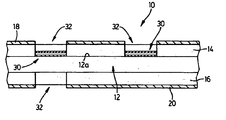
- FIG. 1 is a cross-sectional view of a security substrate in accordance with the present invention
- FIG. 2 is a top plan view of a core layer having highly reflective opaque metal stripes thereon forming part of the security substrate of FIG. 1;
- FIG. 3 is a cross-sectional view of the core layer of FIG. 2 coated with an optically variable thin film multilayer
- FIG. 4 is a top plan view of another embodiment of the core layer having discrete highly reflective opaque metal elements thereon.
- security substrate 10 includes a generally transparent central core layer 12 formed of oriented polypropylene (OPP) disposed between generally transparent, high-density polyethylene (HDPE) layers 14 and 16 .
- the HDPE layers 14 and 16 are secured to the OPP core layer 12 by laminating adhesive resin.
- Opacifying coatings 18 and 20 designed to accept printed indicia cover the HDPE layers 14 and 16 .
- Optically variable devices in the form of interference filters 30 are embedded within the security substrate 10 .
- the interference filters 30 in this example are disposed on one surface 12 a of the OPP core layer 12 and are covered by the HDPE layer 14 .
- the interference filters may be disposed on either or both sides of the OPP core layer 12 .
- Windows 32 are formed in the opacifying coatings 18 and 20 at locations corresponding to the positions of (i.e. in registration with) the interference filters 30 .
- the windows can be formed in one or both opacifying coatings 18 and 20 .
- the OPP and HDPE layers 12 , 14 and 16 respectively form a multilayer substrate similar to that disclosed in U.S. Pat. No. 5,935,696 to Benoit et al, the contents of which are incorporated herein by reference.
- the HDPE layers 14 and 16 are imbalanced biaxially and are oriented in a first direction to a degree that is at least three times less than the degree of orientation in a second direction normal to the first direction.
- the OPP core layer 12 is balanced biaxially and is oriented in a first direction at an orientation ratio of at least 4:1 and oriented in at least a second direction normal to the first direction at an orientation ratio of at least 6:1.
- the HDPE layers 14 and 16 are arranged such that their orientations in the first directions are aligned.
- the interference filters 30 include highly reflective opaque metal stripes 50 formed of aluminum that are disposed on the surface 12 a of OPP core layer 12 (see FIG. 2) and optically variable thin film multilayers 52 disposed on the opaque metal stripes 50 .
- the opaque metal stripes 50 preferably have a reflectance greater than 90% at a 500 nm wavelength and an optical density in the range from about 2.0 and 3.0.
- the opaque metal stripes 50 are patterned on the surface 12 a of the OPP core layer 12 .
- a number of techniques can be used to pattern the opaque metal stripes 50 on the OPP core layer 12 .
- the opaque metal stripes 50 may be patterned on the OPP core layer 12 using an oil patterning process such as those described in U.S. Pat. No. 4,749,591 to Ronchi; U.S. Pat. No. 4,952,420 to Walters; U.S. Pat. No. 4,962,725 to Heinz et al.; U.S. Pat. No. 5,223,038 to Kleyer; and U.S. Pat. No. 5,350,598 to Kleyer.
- a layer of suitable oil is deposited on the OPP core layer 12 prior to vacuum evaporization of the opaque metal stripes on the OPP core layer.
- the oil is applied to the OPP core layer 12 in a vacuum in the evaporization system to create areas where the opaque metal will not nucleate. In this manner, an etchless patterning method for the opaque metal is achieved.
- the opaque metal stripes 50 may be evaporated as thin films onto the surface 12 a of the OPP core layer 12 through a physical mask as is well known.
- the opaque metal stripes may also be patterned on the surface 12 a of the OPP core layer 12 through demetallization using one of two techniques.
- an alkaline etchant solution is printed directly onto the opaque metal in selected areas. The residue is then washed away leaving the patterned metal, which is then evaporated onto the OPP core layer 12 .
- the opaque metal is evaporated onto the OPP core layer 12 .
- a mask in the shape of the desired pattern is then placed over the opaque metal and an alkaline etchant solution is printed directly onto the exposed opaque metal. The residue is then washed away and the mask is removed leaving the patterned opaque metal.
- Using either of these demetallization techniques allows intricate opaque metal patterns to be placed on the OPP core layer 12 with features less than 100 microns in size.
- the opaque metal stripes 50 may also be printed on the surface 12 a of the OPP core layer 12 using metallic high reflectance inks.
- Each optically variable thin film multilayer 52 includes one or more layers of a low refractive index dielectric film identified collectively by reference numeral 60 such as for example, SiO 2 , MgF 2 , Al 2 O 3 etc. or acrylate-based organic compounds, together with a semi-transparent, medium reflective metal layer such as aluminum or alloy such as Inconel (Ni/Cr/Fe alloy) 62 (see FIG. 3 ).
- the layers 60 of dielectric film are evaporated, sputtered or deposited by chemical vapour deposition (CVD) on the OPP core layer 12 over portions of the opaque metal stripes 50 . If an Inconel layer is used, the thickness of the layer is preferably about 10 nm.
- the thickness of the films is preferably in the range of about 170 nm to 480 nm. If Al 2 O 3 dielectric films are used, the thickness of the films is preferably in the range of from about 200 nm to 470 nm. At locations where the optically variable thin film multilayers 52 cover the opaque metal stripes 50 , interference filters 30 are formed that exhibit sharp color shifting characteristics with change in the angle of view.
- the interference filters 30 have well defined characteristics of spectral reflectance and transmittance, both of which vary with the angle of incident of light. As a result, the interference filters 30 provide a sharp color shift that changes with the angle of view.
- the spectral characteristics are of course dependent on the optical constants, refractive indices, absorption coefficients and thicknesses of the security substrate layers. Depending on whether the interference filters 30 are exposed by a window 32 in one opacifying coating 18 or 20 or windows 32 in both opacifying coatings 18 and 20 , different optical effects are achieved.
- windows 32 are provided in both opacifying coatings 18 and 20 , an observer sees an optically variable effect through the window 32 in opacifying coating 18 and a reflective metallic image through the window 32 in opacifying coating 20 that is in registration with the optically variable effect. If a window 32 is only provided in the opacifying coating 18 , only the optically variable effect is visible. If a window 32 is only provided in the opacifying coating 20 , only the reflective metallic image is visible.
- the opaque metal disposed on the OPP core layer 12 need not take the form of stripes 50 as shown in FIG. 2 .
- the opaque metal can be deposited on the surface 12 a of OPP core layer 12 at discrete locations as discrete elements 150 or in intricate patterns 250 .
- the security substrate 10 is described as including an OPP core layer 12 , other biaxially oriented polymers of comparable tensile strength such as linear low-density polyethylene (LLDPE), nylons or polyesters may be used. In cases where high evaporation temperatures are used, PET is preferred.
- LLDPE linear low-density polyethylene
Abstract
A security substrate for a document of value comprises a laminate including a generally transparent core layer and generally transparent outer layers on opposite sides of the core layer. At least one interference filter is embedded within the laminate. The interference filter includes a highly reflective opaque layer on a surface of the core layer and an optically variable thin film multilayer overlying at least a portion of the opaque layer. The interference filter is covered by one of the outer layers.
Description
The present invention relates to document security and in particular to a security substrate for documents of value such as for example, banknotes, credit cards, identification cards and the like.
Documents of value such as identification cards, credit cards, banknotes, etc. are in many cases formed of polymer-based laminates. For example, U.S. Pat. No. 5,935,696 to Benoit et al. discloses a laminated multilayer film substrate having high-density polyethylene layers on each side of an oriented polypropylene layer. The multilayer film substrate exhibits good embossability, dead-fold characteristics and other properties making it suitable for the production of banknotes and other security documents.
Marking documents of value is common practice to deter forgery and allow counterfeit cards and banknotes to be readily detected. For example, U.S. Pat. No. 3,858,977 to Baird et al. discloses an optical interference filter having an optical interference layer with a known characteristic of spectral reflectance and a different known characteristic of spectral transmittance, both of which vary with the angle of incident light on the interference filter. The interference filter is disposed on the banknote substrate over a coloured portion thereof designed to absorb some of the light transmitted by the interference filter so that the interference filer exhibits a colour change with a change in the angle of incident light.
In order to inhibit forgery and counterfeiting, it is desired that security features used to mark documents of value be difficult to copy and highly secured against alteration. Accordingly, improved substrates for documents of value are desired.
It is therefore an object of the present invention to provide a novel security substrate for a document of value and method of forming the same.
According to one aspect of the present invention there is provided a security substrate for a document of value comprising:
a laminate including a generally transparent core layer and a generally transparent outer layer on at least one side of said core layer; and
at least one interference filter embedded within said laminate, said interference layer including a highly reflective opaque layer on a surface of said core layer and an optically variable thin film multilayer overlying at least a portion of said opaque layer, said interference filter being covered by said outer layer.
In a preferred embodiment, the opaque metal layer is patterned on the core layer at spaced locations. The opaque metal layer can be patterned to form continuous stripes or discrete elements that may or may not be intricately patterned.
Preferably, the optically variable thin film multilayer includes one or more dielectric film layers of low refractive index and a semi-transparent, medium reflective layer.
Preferably, generally transparent outer layers are provided on opposite sides of the core layer. Opacifying coatings can be applied to the outer layers and have windows formed therein that are in registration with the interference filter.
According to another aspect of the present invention there is provided a security substrate for a document of value comprising:
a laminate including a generally transparent balanced biaxially oriented core layer, said core layer being oriented in at least a first direction at an orientation ratio of at least 4:1 and oriented in a second direction substantially normal to the first direction at an orientation ratio of at least 6:1; generally transparent imbalanced biaxially oriented outer layers on opposite sides of said core layer, said outer layers being oriented in at least a first direction to a degree which is at least three times less than the degree of orientation present in a second direction substantially normal to the first direction; and a laminating adhesive resin disposed between the outer layers and the core layer to secure the outer layers to the core layer so that the first directions of orientation of the outer layers are substantially aligned;
at least one optically variable device embedded within the laminate, the at least one optically variable device including a highly reflective opaque layer on a surface of said core layer and an optically variable thin film multilayer overlying at least a portion of the opaque layer, said at least one optically variable device being covered by one of said outer layers; and
opacifying coatings on said outer layers, at least one window being formed in at least one of said opacifying coatings that is in registration with said at least one optically variable device.
According to another aspect of the present invention there is provided a method of forming a security substrate for a document of value comprising the steps of:
depositing a highly reflective opaque layer on a surface of a generally transparent core layer;
depositing an optically variable thin film multilayer on said core layer to overlie at least a portion of said opaque layer; and
overlying at least one side of said core layer with a generally transparent outer layer to cover said opaque layer and optically variable thin film multilayer thereby to embed an optically variable device within said security substrate
The present invention provides advantages in that the optically variable interference filter is embedded in the security substrate protecting it from mechanical and chemical attack as well as wear and tear. As a result, the security substrate exhibits high longevity and is highly secured against alternation. Also, since the optically variable interference filter exhibits a sharp color shifting characteristic with changes in the angle of view, the security substrate is virtually impossible to counterfeit using digital methods, laser scanning or photocopying. Furthermore, the security substrate exhibits high tensile strength in the oriented and unoriented directions, good folding and crumple resistance.
Embodiments of the present invention will now be described more fully with reference to the accompanying drawings in which:
FIG. 1 is a cross-sectional view of a security substrate in accordance with the present invention;
FIG. 2 is a top plan view of a core layer having highly reflective opaque metal stripes thereon forming part of the security substrate of FIG. 1;
FIG. 3 is a cross-sectional view of the core layer of FIG. 2 coated with an optically variable thin film multilayer; and
FIG. 4 is a top plan view of another embodiment of the core layer having discrete highly reflective opaque metal elements thereon.
Turning now to FIG. 1, a security substrate in accordance with the present invention is shown and is generally indicated to by reference numeral 10. As can be seen, security substrate 10 includes a generally transparent central core layer 12 formed of oriented polypropylene (OPP) disposed between generally transparent, high-density polyethylene (HDPE) layers 14 and 16. The HDPE layers 14 and 16 are secured to the OPP core layer 12 by laminating adhesive resin. Opacifying coatings 18 and 20 designed to accept printed indicia cover the HDPE layers 14 and 16. Optically variable devices in the form of interference filters 30 are embedded within the security substrate 10. The interference filters 30 in this example are disposed on one surface 12 a of the OPP core layer 12 and are covered by the HDPE layer 14. It will however be appreciated that the interference filters may be disposed on either or both sides of the OPP core layer 12. Windows 32 are formed in the opacifying coatings 18 and 20 at locations corresponding to the positions of (i.e. in registration with) the interference filters 30. Depending on the desired effect, the windows can be formed in one or both opacifying coatings 18 and 20.
In the present embodiment, the OPP and HDPE layers 12, 14 and 16 respectively form a multilayer substrate similar to that disclosed in U.S. Pat. No. 5,935,696 to Benoit et al, the contents of which are incorporated herein by reference. Thus, the HDPE layers 14 and 16 are imbalanced biaxially and are oriented in a first direction to a degree that is at least three times less than the degree of orientation in a second direction normal to the first direction. The OPP core layer 12 is balanced biaxially and is oriented in a first direction at an orientation ratio of at least 4:1 and oriented in at least a second direction normal to the first direction at an orientation ratio of at least 6:1. The HDPE layers 14 and 16 are arranged such that their orientations in the first directions are aligned.
In the present embodiment, the interference filters 30 include highly reflective opaque metal stripes 50 formed of aluminum that are disposed on the surface 12 a of OPP core layer 12 (see FIG. 2) and optically variable thin film multilayers 52 disposed on the opaque metal stripes 50. The opaque metal stripes 50 preferably have a reflectance greater than 90% at a 500 nm wavelength and an optical density in the range from about 2.0 and 3.0.
The opaque metal stripes 50 are patterned on the surface 12 a of the OPP core layer 12. A number of techniques can be used to pattern the opaque metal stripes 50 on the OPP core layer 12. For example, the opaque metal stripes 50 may be patterned on the OPP core layer 12 using an oil patterning process such as those described in U.S. Pat. No. 4,749,591 to Ronchi; U.S. Pat. No. 4,952,420 to Walters; U.S. Pat. No. 4,962,725 to Heinz et al.; U.S. Pat. No. 5,223,038 to Kleyer; and U.S. Pat. No. 5,350,598 to Kleyer. During this process a layer of suitable oil is deposited on the OPP core layer 12 prior to vacuum evaporization of the opaque metal stripes on the OPP core layer. The oil is applied to the OPP core layer 12 in a vacuum in the evaporization system to create areas where the opaque metal will not nucleate. In this manner, an etchless patterning method for the opaque metal is achieved.
Alternatively, the opaque metal stripes 50 may be evaporated as thin films onto the surface 12 a of the OPP core layer 12 through a physical mask as is well known.
The opaque metal stripes may also be patterned on the surface 12 a of the OPP core layer 12 through demetallization using one of two techniques. In one technique, an alkaline etchant solution is printed directly onto the opaque metal in selected areas. The residue is then washed away leaving the patterned metal, which is then evaporated onto the OPP core layer 12. In another technique, the opaque metal is evaporated onto the OPP core layer 12. A mask in the shape of the desired pattern is then placed over the opaque metal and an alkaline etchant solution is printed directly onto the exposed opaque metal. The residue is then washed away and the mask is removed leaving the patterned opaque metal. Using either of these demetallization techniques allows intricate opaque metal patterns to be placed on the OPP core layer 12 with features less than 100 microns in size.
The opaque metal stripes 50 may also be printed on the surface 12 a of the OPP core layer 12 using metallic high reflectance inks.
Each optically variable thin film multilayer 52 includes one or more layers of a low refractive index dielectric film identified collectively by reference numeral 60 such as for example, SiO2, MgF2, Al2O3 etc. or acrylate-based organic compounds, together with a semi-transparent, medium reflective metal layer such as aluminum or alloy such as Inconel (Ni/Cr/Fe alloy) 62 (see FIG. 3). The layers 60 of dielectric film are evaporated, sputtered or deposited by chemical vapour deposition (CVD) on the OPP core layer 12 over portions of the opaque metal stripes 50. If an Inconel layer is used, the thickness of the layer is preferably about 10 nm. If SiO2 dielectric films are used, the thickness of the films is preferably in the range of about 170 nm to 480 nm. If Al2O3 dielectric films are used, the thickness of the films is preferably in the range of from about 200 nm to 470 nm. At locations where the optically variable thin film multilayers 52 cover the opaque metal stripes 50, interference filters 30 are formed that exhibit sharp color shifting characteristics with change in the angle of view.
The interference filters 30 have well defined characteristics of spectral reflectance and transmittance, both of which vary with the angle of incident of light. As a result, the interference filters 30 provide a sharp color shift that changes with the angle of view. The spectral characteristics are of course dependent on the optical constants, refractive indices, absorption coefficients and thicknesses of the security substrate layers. Depending on whether the interference filters 30 are exposed by a window 32 in one opacifying coating 18 or 20 or windows 32 in both opacifying coatings 18 and 20, different optical effects are achieved. If windows 32 are provided in both opacifying coatings 18 and 20, an observer sees an optically variable effect through the window 32 in opacifying coating 18 and a reflective metallic image through the window 32 in opacifying coating 20 that is in registration with the optically variable effect. If a window 32 is only provided in the opacifying coating 18, only the optically variable effect is visible. If a window 32 is only provided in the opacifying coating 20, only the reflective metallic image is visible.
The opaque metal disposed on the OPP core layer 12 need not take the form of stripes 50 as shown in FIG. 2. For example, as shown in FIG. 4, the opaque metal can be deposited on the surface 12 a of OPP core layer 12 at discrete locations as discrete elements 150 or in intricate patterns 250.
Although the security substrate 10 is described as including an OPP core layer 12, other biaxially oriented polymers of comparable tensile strength such as linear low-density polyethylene (LLDPE), nylons or polyesters may be used. In cases where high evaporation temperatures are used, PET is preferred.
Also, although preferred embodiments of the present invention have been described, those of skill in the art will appreciate that variations and/or modifications may be made without departing from the spirit and scope thereof as defined by the appended claims.
Claims (26)
1. A security substrate for a document of value comprising:
a laminate having a generally transparent core layer and a generally transparent outer layer on at least one side of said core layer; and
at least one interference filter embedded within said laminate between said core layer and said outer layer, said interference filter having a highly reflective opaque layer on a surface of said core layer and an optically variable thin film multilayer overlying at least a portion of said opaque layer.
2. A security substrate as defined in claim 1 wherein said opaque layer is patterned on said core layer.
3. A security substrate as defined in claim 2 wherein said opaque layer is patterned on said core layer at spaced locations.
4. A security substrate as defined in claim 3 wherein said opaque layer is patterned to form continuous stripes on said core layer.
5. A security substrate as defined in claim 3 wherein said opaque layer is patterned to form discrete elements on said core layer.
6. A security substrate as defined in claim 5 wherein said discrete elements are individually patterned.
7. A security substrate as defined in claim 3 wherein said opaque layer is formed of aluminum having a reflectance greater than 90% and an optical density in the range of from about 2.0 to 3.0.
8. A security substrate as defined in claim 2 wherein said optically variable thin film multilayer includes one or more dielectric film layers of low refractive index and a semi-transparent, medium reflective layer overlying said one or more dielectric film layers.
9. A security substrate as defined in claim 8 wherein said one or more dielectric film layers is selected from the group consisting of SiO2, MgF2, Al2O3, and acrylate based organic compounds and wherein said medium reflective layer is selected from the group consisting of semi-transparent metals and semi-transparent alloys.
10. A security substrate as defined in claim 9 wherein said semi-transparent metals include aluminum and wherein said semi-transparent alloys include Ni/Cr/Fe.
11. A security substrate as defined in claim 1 wherein said laminate includes generally transparent outer layers on opposite sides of said core layer and wherein said security substrate further includes opacifying coatings on said outer layers, at least one window being formed in one of said opacifying coatings that is in at a location corresponding to said at least one interference filter.
12. A security substrate as defined in claim 11 wherein windows are formed in both opacifying coatings that are at locations corresponding to said at least one interference filter.
13. A security substrate as defined in claim 2 wherein said core layer is formed of oriented polypropylene and wherein said outer layer is formed of high-density polyethylene.
14. A security substrate as defined in claim 11 in the form of a banknote.
15. A security substrate for a document of value comprising:
a laminate having a generally transparent balanced biaxially oriented core layer, said core layer being oriented in at least a first direction at an orientation ratio of at least 4:1 and oriented in a second direction substantially normal to the first direction at an orientation ratio of at least 6:1; generally transparent imbalanced biaxially oriented outer layers on opposite sides of said core layer, said outer layers being oriented in at least a first direction to a degree which is at least three times less than the degree of orientation present in a second direction substantially normal to the first direction; and a laminating adhesive resin securing the outer layers to the core layer so that the first directions of orientation of the outer layers are substantially aligned;
at least one optically variable device embedded within the laminate between said core layer and one of said cover layers, the at least one optically variable device having a highly reflective opaque layer on a surface of said core layer and an optically variable thin film multilayer overlying at least a portion of the opaque layer; and
opacifying coatings on said outer layers, at least one window being formed in at least one of said opacifying coatings that is at a location corresponding to said at least one optically variable device.
16. A security substrate as defined in claim 15 in the form of a banknote.
17. A security substrate as defined in claim 16 wherein said opaque layer is patterned on said core layer.
18. A security substrate as defined in claim 17 wherein said opaque layer is formed of aluminum having a reflectance greater than 90% and an optical density in the range of from about 2.0 to 3.0.
19. A security substrate as defined in claim 18 wherein said optically variable thin film multilayer includes one or more dielectric film layers of low refractive index and a semi-transparent, medium reflective layer overlying said one or more dielectric film layers.
20. A security substrate as defined in claim 18 wherein said one or more dielectric film layers is selected from the group consisting of SiO2, MgF2, Al2O3, and acrylate based organic compounds and wherein said medium reflective layer is selected from the group consisting of semi-transparent metals and semi-transparent alloys.
21. A security substrate as defined in claim 20 wherein said semi-transparent metals include aluminum and wherein said semi-transparent alloys include Ni/Cr/Fe.
22. A security substrate as defined in claim 1 wherein said opaque layer is formed of metallic high reflectance ink.
23. A security substrate as defined in claim 16 wherein said opaque layer is formed of metallic high reflectance ink.
24. A security substrate as defined in claim 16 wherein windows are formed in both of said opacifying coatings at locations corresponding to said at least one optically variable devices.
25. A security substrate as defined in claim 16 including a plurality of optically variable devices embedded within said laminate between said core layer and an outer layer at discrete locations, a window being formed in said opacifying coatings for each of said optically variable devices.
26. A security substrate as defined in claim 25 wherein windows are formed in both of said opacifying coatings for at least one of said optically variable devices.
Priority Applications (1)
| Application Number | Priority Date | Filing Date | Title |
|---|---|---|---|
| US09/669,425 US6686027B1 (en) | 2000-09-25 | 2000-09-25 | Security substrate for documents of value |
Applications Claiming Priority (1)
| Application Number | Priority Date | Filing Date | Title |
|---|---|---|---|
| US09/669,425 US6686027B1 (en) | 2000-09-25 | 2000-09-25 | Security substrate for documents of value |
Publications (1)
| Publication Number | Publication Date |
|---|---|
| US6686027B1 true US6686027B1 (en) | 2004-02-03 |
Family
ID=30444371
Family Applications (1)
| Application Number | Title | Priority Date | Filing Date |
|---|---|---|---|
| US09/669,425 Expired - Fee Related US6686027B1 (en) | 2000-09-25 | 2000-09-25 | Security substrate for documents of value |
Country Status (1)
| Country | Link |
|---|---|
| US (1) | US6686027B1 (en) |
Cited By (41)
| Publication number | Priority date | Publication date | Assignee | Title |
|---|---|---|---|---|
| US20030012935A1 (en) * | 2001-07-02 | 2003-01-16 | Merck Patent Gmbh | Optically variable marking |
| US20050042449A1 (en) * | 2003-07-14 | 2005-02-24 | Jds Uniphase Corporation, | Vacuum roll coated security thin film interference products with overt and/or covert patterned layers |
| US20050104364A1 (en) * | 2001-12-21 | 2005-05-19 | Giesecke & Devrient Gmbh | Security element for security papers and valuable documents |
| US20050106367A1 (en) * | 2002-07-15 | 2005-05-19 | Jds Uniphase Corporation | Method and apparatus for orienting magnetic flakes |
| US20050127663A1 (en) * | 2002-02-14 | 2005-06-16 | Manfred Heim | Security element and security document with one such security element |
| US20050151368A1 (en) * | 2002-02-22 | 2005-07-14 | Manfred Heim | Security document and security element for a security document |
| US20060035080A1 (en) * | 2002-09-13 | 2006-02-16 | Jds Uniphase Corporation | Provision of frames or borders around opaque flakes for covert security applications |
| US20060077496A1 (en) * | 1999-07-08 | 2006-04-13 | Jds Uniphase Corporation | Patterned structures with optically variable effects |
| US20060097515A1 (en) * | 2002-07-15 | 2006-05-11 | Jds Uniphase Corporation | Kinematic images formed by orienting alignable flakes |
| US20060194040A1 (en) * | 2002-09-13 | 2006-08-31 | Jds Uniphase Corporation | Two-step method of coating an article for security printing |
| US20060198998A1 (en) * | 2002-07-15 | 2006-09-07 | Jds Uniphase Corporation | Dynamic appearance-changing optical devices (dacod) printed in a shaped magnetic field including printable fresnel structures |
| US20060263539A1 (en) * | 2002-07-15 | 2006-11-23 | Jds Uniphase Corporation | Alignable Diffractive Pigment Flakes And Method And Apparatus For Alignment And Images Formed Therefrom |
| US20070058227A1 (en) * | 1999-07-08 | 2007-03-15 | Jds Uniphase Corporation | Patterned Optical Structures With Enhanced Security Feature |
| WO2007070969A1 (en) * | 2005-12-23 | 2007-06-28 | Securency International Pty Ltd | Tamper evident security document with coloured layer |
| US20070172261A1 (en) * | 2002-07-15 | 2007-07-26 | Jds Uniphase Corporation | Apparatus For Orienting Magnetic Flakes |
| US20070183047A1 (en) * | 2000-01-21 | 2007-08-09 | Jds Uniphase Corporation | Optically Variable Security Devices |
| US20070195392A1 (en) * | 1999-07-08 | 2007-08-23 | Jds Uniphase Corporation | Adhesive Chromagram And Method Of Forming Thereof |
| US20070241553A1 (en) * | 2004-10-07 | 2007-10-18 | Giesecke & Devrient Gmbh | Security Ekement Provided with an Optically-Variable Layer and Method for The Production Thereod |
| EP1854642A2 (en) | 2006-05-12 | 2007-11-14 | JDS Uniphase Corporation | A security device formed by a hologram and a color shifting ink |
| US20070292636A1 (en) * | 1999-07-08 | 2007-12-20 | Jds Uniphase Corporation. | Security Device Having A Segmented Layer |
| US20080003413A1 (en) * | 2002-09-13 | 2008-01-03 | Jds Uniphase Corporation | Stamping A Coating Of Cured Field Aligned Special Effect Flakes And Image Formed Thereby |
| US20080019924A1 (en) * | 2003-08-14 | 2008-01-24 | Jds Uniphase Corporation | Non-Toxic Flakes For Authentication Of Pharmaceutical Articles |
| US20080019003A1 (en) * | 2003-07-14 | 2008-01-24 | Jds Uniphase Corporation | Vacuum Roll Coated Security Thin Film Interference Products With Overt And/Or Covert Patterned Layers |
| US20080107856A1 (en) * | 2002-09-13 | 2008-05-08 | Jds Uniphase Corporation | Provision of Frames Or Borders Around Pigment Flakes For Covert Security Applications |
| US20080171144A1 (en) * | 2002-09-13 | 2008-07-17 | Jds Uniphase Corporation | Printed Magnetic Ink Overt Security Image |
| US20080236447A1 (en) * | 2002-09-13 | 2008-10-02 | Jds Uniphase Corporation | Flake For Covert Security Applications |
| WO2010043846A1 (en) * | 2008-10-16 | 2010-04-22 | De La Rue International Limited | Improvements in printed security features |
| US20100208351A1 (en) * | 2002-07-15 | 2010-08-19 | Nofi Michael R | Selective and oriented assembly of platelet materials and functional additives |
| US8465625B2 (en) | 2001-12-21 | 2013-06-18 | Giesecke & Devrient Gmbh | Security paper and method and apparatus for producing the same |
| US20130280506A1 (en) * | 2008-07-01 | 2013-10-24 | Ian William Bain | Authentication of articles |
| US8658280B2 (en) | 2002-09-13 | 2014-02-25 | Jds Uniphase Corporation | Taggent flakes for covert security applications having a selected shape |
| US20140106091A1 (en) * | 2006-05-12 | 2014-04-17 | Rolic Ag | Optically effective surface relief microstructures and method of making them |
| EP2590822B1 (en) | 2010-07-05 | 2015-05-06 | Giesecke & Devrient GmbH | Value document with a transparent ink-accepting layer and with an opaque ink-accepting layer |
| US9027479B2 (en) | 2002-07-15 | 2015-05-12 | Jds Uniphase Corporation | Method and apparatus for orienting magnetic flakes |
| US9102195B2 (en) | 2012-01-12 | 2015-08-11 | Jds Uniphase Corporation | Article with curved patterns formed of aligned pigment flakes |
| US20150376841A1 (en) * | 2013-02-15 | 2015-12-31 | Kba-Notasys Sa | Substrate for security papers and method of manufacturing the same |
| US9458324B2 (en) | 2002-09-13 | 2016-10-04 | Viava Solutions Inc. | Flakes with undulate borders and method of forming thereof |
| CN107614278A (en) * | 2015-06-10 | 2018-01-19 | Ccl证券私人有限公司 | Optical devices with hiding description |
| WO2020128554A1 (en) * | 2018-12-17 | 2020-06-25 | Linxens Holding | A pre-laminate for a datapage of a security document and method of forming the same |
| US11230127B2 (en) | 2002-07-15 | 2022-01-25 | Viavi Solutions Inc. | Method and apparatus for orienting magnetic flakes |
| US11768321B2 (en) | 2000-01-21 | 2023-09-26 | Viavi Solutions Inc. | Optically variable security devices |
Citations (11)
| Publication number | Priority date | Publication date | Assignee | Title |
|---|---|---|---|---|
| US3858977A (en) | 1972-01-18 | 1975-01-07 | Canadian Patents Dev | Optical interference authenticating means |
| US4749591A (en) | 1985-07-03 | 1988-06-07 | Metalvuoto Films S.P.A. | Device for making metallized plastic films with clearly defined non-metallized areas |
| US4952420A (en) | 1988-10-12 | 1990-08-28 | Advanced Dielectric Technologies, Inc. | Vapor deposition patterning method |
| US4962725A (en) | 1989-07-06 | 1990-10-16 | Leybold Aktiengesellschaft | Apparatus for producing metal-free strips on vacuum-coated film webs, particularly to be used with capacitors |
| US5223038A (en) | 1991-01-11 | 1993-06-29 | Leybold Ag | Apparatus for producing metal-free strips |
| US5350598A (en) | 1993-03-27 | 1994-09-27 | Leybold Aktiengesellschaft | Apparatus and method for selectively coating a substrate in strip form |
| US5425996A (en) * | 1994-04-05 | 1995-06-20 | Borden, Inc. | Biaxially oriented polypropylene metallized white film |
| US5492370A (en) * | 1991-03-22 | 1996-02-20 | De La Rue Holographics Ltd. | Decorative article |
| US5935696A (en) | 1997-06-11 | 1999-08-10 | Mobil Oil Corporation | Multilayer film structures for use in the production of banknotes or the like |
| US6294267B1 (en) * | 1994-06-27 | 2001-09-25 | Exxonmobil Oil Corporation | Core printed security documents |
| US6318758B1 (en) * | 1995-12-22 | 2001-11-20 | Giesecke & Devrient Gmbh | Security document with a security component and method for the production thereof |
-
2000
- 2000-09-25 US US09/669,425 patent/US6686027B1/en not_active Expired - Fee Related
Patent Citations (11)
| Publication number | Priority date | Publication date | Assignee | Title |
|---|---|---|---|---|
| US3858977A (en) | 1972-01-18 | 1975-01-07 | Canadian Patents Dev | Optical interference authenticating means |
| US4749591A (en) | 1985-07-03 | 1988-06-07 | Metalvuoto Films S.P.A. | Device for making metallized plastic films with clearly defined non-metallized areas |
| US4952420A (en) | 1988-10-12 | 1990-08-28 | Advanced Dielectric Technologies, Inc. | Vapor deposition patterning method |
| US4962725A (en) | 1989-07-06 | 1990-10-16 | Leybold Aktiengesellschaft | Apparatus for producing metal-free strips on vacuum-coated film webs, particularly to be used with capacitors |
| US5223038A (en) | 1991-01-11 | 1993-06-29 | Leybold Ag | Apparatus for producing metal-free strips |
| US5492370A (en) * | 1991-03-22 | 1996-02-20 | De La Rue Holographics Ltd. | Decorative article |
| US5350598A (en) | 1993-03-27 | 1994-09-27 | Leybold Aktiengesellschaft | Apparatus and method for selectively coating a substrate in strip form |
| US5425996A (en) * | 1994-04-05 | 1995-06-20 | Borden, Inc. | Biaxially oriented polypropylene metallized white film |
| US6294267B1 (en) * | 1994-06-27 | 2001-09-25 | Exxonmobil Oil Corporation | Core printed security documents |
| US6318758B1 (en) * | 1995-12-22 | 2001-11-20 | Giesecke & Devrient Gmbh | Security document with a security component and method for the production thereof |
| US5935696A (en) | 1997-06-11 | 1999-08-10 | Mobil Oil Corporation | Multilayer film structures for use in the production of banknotes or the like |
Cited By (86)
| Publication number | Priority date | Publication date | Assignee | Title |
|---|---|---|---|---|
| US20070292636A1 (en) * | 1999-07-08 | 2007-12-20 | Jds Uniphase Corporation. | Security Device Having A Segmented Layer |
| US7667895B2 (en) | 1999-07-08 | 2010-02-23 | Jds Uniphase Corporation | Patterned structures with optically variable effects |
| US20070195392A1 (en) * | 1999-07-08 | 2007-08-23 | Jds Uniphase Corporation | Adhesive Chromagram And Method Of Forming Thereof |
| US20070058227A1 (en) * | 1999-07-08 | 2007-03-15 | Jds Uniphase Corporation | Patterned Optical Structures With Enhanced Security Feature |
| US20060077496A1 (en) * | 1999-07-08 | 2006-04-13 | Jds Uniphase Corporation | Patterned structures with optically variable effects |
| US7876481B2 (en) | 1999-07-08 | 2011-01-25 | Jds Uniphase Corporation | Patterned optical structures with enhanced security feature |
| US7880943B2 (en) | 1999-07-08 | 2011-02-01 | Jds Uniphase Corporation | Patterned optical structures with enhanced security feature |
| US7754112B2 (en) | 1999-07-08 | 2010-07-13 | Jds Uniphase Corporation | Methods for forming security articles having diffractive surfaces and color shifting backgrounds |
| US11768321B2 (en) | 2000-01-21 | 2023-09-26 | Viavi Solutions Inc. | Optically variable security devices |
| US20070183047A1 (en) * | 2000-01-21 | 2007-08-09 | Jds Uniphase Corporation | Optically Variable Security Devices |
| US7081282B2 (en) * | 2001-07-02 | 2006-07-25 | Merck Patent Gmbh | Optically variable marking |
| US20030012935A1 (en) * | 2001-07-02 | 2003-01-16 | Merck Patent Gmbh | Optically variable marking |
| US9257059B2 (en) | 2001-07-31 | 2016-02-09 | Viavi Solutions Inc. | Dynamic appearance-changing optical devices (DACOD) printed in a shaped magnetic field including printable fresnel structures |
| US8465625B2 (en) | 2001-12-21 | 2013-06-18 | Giesecke & Devrient Gmbh | Security paper and method and apparatus for producing the same |
| US8449969B2 (en) * | 2001-12-21 | 2013-05-28 | Giesecke & Devrient Gmbh | Security element for security papers and valuable documents |
| US20050104364A1 (en) * | 2001-12-21 | 2005-05-19 | Giesecke & Devrient Gmbh | Security element for security papers and valuable documents |
| US7699350B2 (en) * | 2002-02-14 | 2010-04-20 | Giesecke & Devrient Gmbh | Security element and security document with one such security element |
| US20050127663A1 (en) * | 2002-02-14 | 2005-06-16 | Manfred Heim | Security element and security document with one such security element |
| US7611168B2 (en) * | 2002-02-22 | 2009-11-03 | Giesecke & Devrient Gmbh | Security document and security element for a security document |
| US20050151368A1 (en) * | 2002-02-22 | 2005-07-14 | Manfred Heim | Security document and security element for a security document |
| US20100208351A1 (en) * | 2002-07-15 | 2010-08-19 | Nofi Michael R | Selective and oriented assembly of platelet materials and functional additives |
| US10059137B2 (en) | 2002-07-15 | 2018-08-28 | Viavi Solutions Inc. | Apparatus for orienting magnetic flakes |
| US8343615B2 (en) | 2002-07-15 | 2013-01-01 | Jds Uniphase Corporation | Dynamic appearance-changing optical devices (DACOD) printed in a shaped magnetic field including printable fresnel structures |
| US20060263539A1 (en) * | 2002-07-15 | 2006-11-23 | Jds Uniphase Corporation | Alignable Diffractive Pigment Flakes And Method And Apparatus For Alignment And Images Formed Therefrom |
| US20060198998A1 (en) * | 2002-07-15 | 2006-09-07 | Jds Uniphase Corporation | Dynamic appearance-changing optical devices (dacod) printed in a shaped magnetic field including printable fresnel structures |
| US8726806B2 (en) | 2002-07-15 | 2014-05-20 | Jds Uniphase Corporation | Apparatus for orienting magnetic flakes |
| US7934451B2 (en) | 2002-07-15 | 2011-05-03 | Jds Uniphase Corporation | Apparatus for orienting magnetic flakes |
| US10173455B2 (en) | 2002-07-15 | 2019-01-08 | Viavi Solutions Inc. | Dynamic appearance-changing optical devices (DACOD) printed in a shaped magnetic field including printable fresnel structures |
| US20070172261A1 (en) * | 2002-07-15 | 2007-07-26 | Jds Uniphase Corporation | Apparatus For Orienting Magnetic Flakes |
| US9027479B2 (en) | 2002-07-15 | 2015-05-12 | Jds Uniphase Corporation | Method and apparatus for orienting magnetic flakes |
| US20060097515A1 (en) * | 2002-07-15 | 2006-05-11 | Jds Uniphase Corporation | Kinematic images formed by orienting alignable flakes |
| US7517578B2 (en) | 2002-07-15 | 2009-04-14 | Jds Uniphase Corporation | Method and apparatus for orienting magnetic flakes |
| US7604855B2 (en) | 2002-07-15 | 2009-10-20 | Jds Uniphase Corporation | Kinematic images formed by orienting alignable flakes |
| US9522402B2 (en) | 2002-07-15 | 2016-12-20 | Viavi Solutions Inc. | Method and apparatus for orienting magnetic flakes |
| US11230127B2 (en) | 2002-07-15 | 2022-01-25 | Viavi Solutions Inc. | Method and apparatus for orienting magnetic flakes |
| US20050106367A1 (en) * | 2002-07-15 | 2005-05-19 | Jds Uniphase Corporation | Method and apparatus for orienting magnetic flakes |
| US20080107856A1 (en) * | 2002-09-13 | 2008-05-08 | Jds Uniphase Corporation | Provision of Frames Or Borders Around Pigment Flakes For Covert Security Applications |
| USRE45762E1 (en) | 2002-09-13 | 2015-10-20 | Jds Uniphase Corporation | Printed magnetic ink overt security image |
| US20080171144A1 (en) * | 2002-09-13 | 2008-07-17 | Jds Uniphase Corporation | Printed Magnetic Ink Overt Security Image |
| US9164575B2 (en) | 2002-09-13 | 2015-10-20 | Jds Uniphase Corporation | Provision of frames or borders around pigment flakes for covert security applications |
| US20060035080A1 (en) * | 2002-09-13 | 2006-02-16 | Jds Uniphase Corporation | Provision of frames or borders around opaque flakes for covert security applications |
| US9458324B2 (en) | 2002-09-13 | 2016-10-04 | Viava Solutions Inc. | Flakes with undulate borders and method of forming thereof |
| US20080236447A1 (en) * | 2002-09-13 | 2008-10-02 | Jds Uniphase Corporation | Flake For Covert Security Applications |
| US8999616B2 (en) | 2002-09-13 | 2015-04-07 | Jds Uniphase Corporation | Taggent flakes for covert security applications having a selected shape |
| US7674501B2 (en) | 2002-09-13 | 2010-03-09 | Jds Uniphase Corporation | Two-step method of coating an article for security printing by application of electric or magnetic field |
| US8025952B2 (en) | 2002-09-13 | 2011-09-27 | Jds Uniphase Corporation | Printed magnetic ink overt security image |
| US8118963B2 (en) | 2002-09-13 | 2012-02-21 | Alberto Argoitia | Stamping a coating of cured field aligned special effect flakes and image formed thereby |
| US20080003413A1 (en) * | 2002-09-13 | 2008-01-03 | Jds Uniphase Corporation | Stamping A Coating Of Cured Field Aligned Special Effect Flakes And Image Formed Thereby |
| US7645510B2 (en) | 2002-09-13 | 2010-01-12 | Jds Uniphase Corporation | Provision of frames or borders around opaque flakes for covert security applications |
| US8658280B2 (en) | 2002-09-13 | 2014-02-25 | Jds Uniphase Corporation | Taggent flakes for covert security applications having a selected shape |
| US20060194040A1 (en) * | 2002-09-13 | 2006-08-31 | Jds Uniphase Corporation | Two-step method of coating an article for security printing |
| US20070275189A1 (en) * | 2003-07-14 | 2007-11-29 | Jds Uniphase Corporation. | Vacuum Roll Coated Security Thin Film Interference Products With Overt And/Or Covert Patterned Layers |
| US20080019003A1 (en) * | 2003-07-14 | 2008-01-24 | Jds Uniphase Corporation | Vacuum Roll Coated Security Thin Film Interference Products With Overt And/Or Covert Patterned Layers |
| EP1498545B1 (en) | 2003-07-14 | 2017-09-27 | Flex Products, Inc. a JDS Uniphase Company | Security thread comprising an optically variable structure |
| US20070273147A1 (en) * | 2003-07-14 | 2007-11-29 | Jds Uniphase Corporation | Vacuum Roll Coated Security Thin Film Interference Products With Overt And/Or Covert Patterned Layers |
| US20070273144A1 (en) * | 2003-07-14 | 2007-11-29 | Jds Uniphase Corporation | Vacuum Roll Coated Security Thin Film Interference Products With Overt And/Or Covert Patterned Layers |
| US7744964B2 (en) * | 2003-07-14 | 2010-06-29 | Jds Uniphase Corporation | Vacuum roll coated security thin film interference products with overt and/or covert patterned layers |
| US20070296204A1 (en) * | 2003-07-14 | 2007-12-27 | Jds Uniphase Corporation | Vacuum Roll Coated Security Thin Film Interference Products With Overt And/Or Covert Patterned Layers |
| US20050042449A1 (en) * | 2003-07-14 | 2005-02-24 | Jds Uniphase Corporation, | Vacuum roll coated security thin film interference products with overt and/or covert patterned layers |
| US20080019924A1 (en) * | 2003-08-14 | 2008-01-24 | Jds Uniphase Corporation | Non-Toxic Flakes For Authentication Of Pharmaceutical Articles |
| US20070241553A1 (en) * | 2004-10-07 | 2007-10-18 | Giesecke & Devrient Gmbh | Security Ekement Provided with an Optically-Variable Layer and Method for The Production Thereod |
| US8276945B2 (en) * | 2004-10-07 | 2012-10-02 | Giesecke & Devrient Gmbh | Security element provided with an optically-variable layer and method for the production thereof |
| WO2007070969A1 (en) * | 2005-12-23 | 2007-06-28 | Securency International Pty Ltd | Tamper evident security document with coloured layer |
| EP1854642A2 (en) | 2006-05-12 | 2007-11-14 | JDS Uniphase Corporation | A security device formed by a hologram and a color shifting ink |
| US10350843B2 (en) * | 2006-05-12 | 2019-07-16 | Rolic Ag | Optically effective surface relief microstructures and method of making them |
| US20140106091A1 (en) * | 2006-05-12 | 2014-04-17 | Rolic Ag | Optically effective surface relief microstructures and method of making them |
| US9355296B2 (en) * | 2008-07-01 | 2016-05-31 | Innovia Films Limited | Authentication of articles |
| US20130280506A1 (en) * | 2008-07-01 | 2013-10-24 | Ian William Bain | Authentication of articles |
| WO2010043846A1 (en) * | 2008-10-16 | 2010-04-22 | De La Rue International Limited | Improvements in printed security features |
| EA023526B1 (en) * | 2008-10-16 | 2016-06-30 | Де Ля Рю Интернэшнл Лимитед | Improvements in printed security features |
| CN102186677B (en) * | 2008-10-16 | 2013-01-30 | 德拉鲁国际公司 | Improvements in printed security features |
| EP2590822B1 (en) | 2010-07-05 | 2015-05-06 | Giesecke & Devrient GmbH | Value document with a transparent ink-accepting layer and with an opaque ink-accepting layer |
| EP2590822B2 (en) † | 2010-07-05 | 2022-07-13 | Giesecke+Devrient Currency Technology GmbH | Value document with a transparent ink-accepting layer and with an opaque ink-accepting layer |
| US10562333B2 (en) | 2012-01-12 | 2020-02-18 | Viavi Solutions Inc. | Article with curved patterns formed of aligned pigment flakes |
| US10259254B2 (en) | 2012-01-12 | 2019-04-16 | Viavi Solutions Inc. | Article with a dynamic frame formed with aligned pigment flakes |
| US10232660B2 (en) | 2012-01-12 | 2019-03-19 | Viavi Solutions Inc. | Article with curved patterns formed of aligned pigment flakes |
| US10752042B2 (en) | 2012-01-12 | 2020-08-25 | Viavi Solutions Inc. | Article with dynamic frame formed with aligned pigment flakes |
| US11198315B2 (en) | 2012-01-12 | 2021-12-14 | Viavi Solutions Inc. | Article with curved patterns formed of aligned pigment flakes |
| US9102195B2 (en) | 2012-01-12 | 2015-08-11 | Jds Uniphase Corporation | Article with curved patterns formed of aligned pigment flakes |
| US9598821B2 (en) * | 2013-02-15 | 2017-03-21 | Kba-Notasys Sa | Substrate for security papers and method of manufacturing the same |
| US20150376841A1 (en) * | 2013-02-15 | 2015-12-31 | Kba-Notasys Sa | Substrate for security papers and method of manufacturing the same |
| CN107614278A (en) * | 2015-06-10 | 2018-01-19 | Ccl证券私人有限公司 | Optical devices with hiding description |
| WO2020128554A1 (en) * | 2018-12-17 | 2020-06-25 | Linxens Holding | A pre-laminate for a datapage of a security document and method of forming the same |
| CN113195242A (en) * | 2018-12-17 | 2021-07-30 | 兰克森控股公司 | Prelaminate for data pages of security documents and method of forming the same |
| US20220055394A1 (en) * | 2018-12-17 | 2022-02-24 | Linxens Holding | A pre-laminate for a datapage of a security document and method of forming the same |
| CN113195242B (en) * | 2018-12-17 | 2022-09-20 | 兰克森控股公司 | Prelaminate for data pages of security documents and method of forming the same |
Similar Documents
| Publication | Publication Date | Title |
|---|---|---|
| US6686027B1 (en) | Security substrate for documents of value | |
| CA2377522C (en) | Method of producing a diffractive structure in security documents | |
| US7782509B2 (en) | Security device | |
| US8603615B2 (en) | Security element | |
| RU2483934C2 (en) | Protective element and method of its manufacturing | |
| EP1498545B1 (en) | Security thread comprising an optically variable structure | |
| KR100619121B1 (en) | Inorganic sheet carrying symbols for making pigments | |
| CN100567022C (en) | Security element and have the security document of this Security element | |
| RU2313456C2 (en) | Protective element with color kipp effect and magnetic properties, object with such a protective element, and method for manufacturing such protective element and such object | |
| CN109895526B (en) | Optical anti-counterfeiting element and manufacturing method thereof | |
| EP3445592B1 (en) | Security devices and methods of manufacture thereof | |
| US20080019003A1 (en) | Vacuum Roll Coated Security Thin Film Interference Products With Overt And/Or Covert Patterned Layers | |
| KR20010053105A (en) | Improvements in security documents and substrates therefor | |
| CN110712451B (en) | Optical anti-counterfeiting element, preparation method thereof and optical anti-counterfeiting product | |
| JPH1158581A (en) | Laminated material for preventing forgery | |
| CN111098620A (en) | Optical anti-counterfeiting element, preparation method of optical anti-counterfeiting element and optical anti-counterfeiting product | |
| KR101785467B1 (en) | Dual color-shifting security element and method for producing it, security product comprising it | |
| RU2743283C1 (en) | Holographic element for security labels and tapes | |
| JP2010173220A (en) | Forgery prevention medium | |
| JPH0997011A (en) | Seal | |
| EP4271572A1 (en) | Security element for documents, particularly banknotes, and method for its production | |
| KR20210073137A (en) | Color-shifting security film and security product comprising the same | |
| KR20210073138A (en) | Security film and security product comprising the same |
Legal Events
| Date | Code | Title | Description |
|---|---|---|---|
| AS | Assignment |
Owner name: AGRA VADEKO INC., CANADA Free format text: ASSIGNMENT OF ASSIGNORS INTEREST;ASSIGNORS:CAPORALETTI, OMAR;DISANO, JOHN NICHOLAS;SCOTT, JACK;REEL/FRAME:011133/0610;SIGNING DATES FROM 20000911 TO 20000915 |
|
| REMI | Maintenance fee reminder mailed | ||
| LAPS | Lapse for failure to pay maintenance fees | ||
| STCH | Information on status: patent discontinuation |
Free format text: PATENT EXPIRED DUE TO NONPAYMENT OF MAINTENANCE FEES UNDER 37 CFR 1.362 |
|
| FP | Lapsed due to failure to pay maintenance fee |
Effective date: 20080203 |