US6683645B1 - Imaging system with low sensitivity to variation in scene illumination - Google Patents
Imaging system with low sensitivity to variation in scene illumination Download PDFInfo
- Publication number
- US6683645B1 US6683645B1 US09/068,887 US6888798A US6683645B1 US 6683645 B1 US6683645 B1 US 6683645B1 US 6888798 A US6888798 A US 6888798A US 6683645 B1 US6683645 B1 US 6683645B1
- Authority
- US
- United States
- Prior art keywords
- pixel
- floating gate
- circuit
- mosfet
- output
- Prior art date
- Legal status (The legal status is an assumption and is not a legal conclusion. Google has not performed a legal analysis and makes no representation as to the accuracy of the status listed.)
- Expired - Lifetime
Links
- 238000003384 imaging method Methods 0.000 title claims abstract description 44
- 238000005286 illumination Methods 0.000 title claims description 33
- 230000035945 sensitivity Effects 0.000 title description 7
- 238000001914 filtration Methods 0.000 claims abstract description 33
- 238000007667 floating Methods 0.000 claims description 89
- 238000000034 method Methods 0.000 claims description 44
- 230000004044 response Effects 0.000 claims description 44
- 238000012935 Averaging Methods 0.000 claims description 42
- 238000012545 processing Methods 0.000 claims description 30
- 230000005855 radiation Effects 0.000 claims description 21
- 230000008569 process Effects 0.000 claims description 17
- 230000002829 reductive effect Effects 0.000 claims description 11
- 238000003860 storage Methods 0.000 claims description 5
- 238000010606 normalization Methods 0.000 claims description 4
- 230000005670 electromagnetic radiation Effects 0.000 claims description 3
- 238000002347 injection Methods 0.000 claims 2
- 239000007924 injection Substances 0.000 claims 2
- 238000001514 detection method Methods 0.000 abstract 2
- 238000009966 trimming Methods 0.000 description 17
- 230000008859 change Effects 0.000 description 14
- 238000009826 distribution Methods 0.000 description 14
- 230000005540 biological transmission Effects 0.000 description 13
- 230000000694 effects Effects 0.000 description 12
- 238000004088 simulation Methods 0.000 description 12
- 238000012937 correction Methods 0.000 description 11
- 210000001525 retina Anatomy 0.000 description 11
- 230000001419 dependent effect Effects 0.000 description 10
- 230000009897 systematic effect Effects 0.000 description 10
- 238000006243 chemical reaction Methods 0.000 description 8
- 235000019988 mead Nutrition 0.000 description 8
- 239000000758 substrate Substances 0.000 description 8
- 230000006870 function Effects 0.000 description 7
- 210000002569 neuron Anatomy 0.000 description 7
- 230000004907 flux Effects 0.000 description 5
- 230000008901 benefit Effects 0.000 description 4
- 230000008878 coupling Effects 0.000 description 4
- 238000010168 coupling process Methods 0.000 description 4
- 238000005859 coupling reaction Methods 0.000 description 4
- 238000010586 diagram Methods 0.000 description 4
- 230000005669 field effect Effects 0.000 description 4
- 230000009467 reduction Effects 0.000 description 4
- 230000003042 antagnostic effect Effects 0.000 description 3
- 238000013459 approach Methods 0.000 description 3
- 210000001052 bipolar neuron Anatomy 0.000 description 3
- 238000013500 data storage Methods 0.000 description 3
- 230000003247 decreasing effect Effects 0.000 description 3
- 210000004205 output neuron Anatomy 0.000 description 3
- 229910021420 polycrystalline silicon Inorganic materials 0.000 description 3
- 230000015556 catabolic process Effects 0.000 description 2
- 230000006835 compression Effects 0.000 description 2
- 238000007906 compression Methods 0.000 description 2
- 230000007423 decrease Effects 0.000 description 2
- 238000013461 design Methods 0.000 description 2
- 239000007943 implant Substances 0.000 description 2
- 238000004519 manufacturing process Methods 0.000 description 2
- 239000002184 metal Substances 0.000 description 2
- 239000004065 semiconductor Substances 0.000 description 2
- 230000000007 visual effect Effects 0.000 description 2
- 238000012952 Resampling Methods 0.000 description 1
- XUIMIQQOPSSXEZ-UHFFFAOYSA-N Silicon Chemical compound [Si] XUIMIQQOPSSXEZ-UHFFFAOYSA-N 0.000 description 1
- 238000004458 analytical method Methods 0.000 description 1
- 238000003491 array Methods 0.000 description 1
- 230000002238 attenuated effect Effects 0.000 description 1
- 238000004364 calculation method Methods 0.000 description 1
- 239000003990 capacitor Substances 0.000 description 1
- 230000000295 complement effect Effects 0.000 description 1
- 230000001010 compromised effect Effects 0.000 description 1
- 238000006731 degradation reaction Methods 0.000 description 1
- 230000003111 delayed effect Effects 0.000 description 1
- 238000009792 diffusion process Methods 0.000 description 1
- 238000005516 engineering process Methods 0.000 description 1
- 238000010348 incorporation Methods 0.000 description 1
- 230000010365 information processing Effects 0.000 description 1
- 230000000670 limiting effect Effects 0.000 description 1
- 230000007246 mechanism Effects 0.000 description 1
- 229910044991 metal oxide Inorganic materials 0.000 description 1
- 150000004706 metal oxides Chemical class 0.000 description 1
- 230000003278 mimic effect Effects 0.000 description 1
- 230000001537 neural effect Effects 0.000 description 1
- 238000007639 printing Methods 0.000 description 1
- 238000002310 reflectometry Methods 0.000 description 1
- 230000006335 response to radiation Effects 0.000 description 1
- 230000000717 retained effect Effects 0.000 description 1
- 229910052710 silicon Inorganic materials 0.000 description 1
- 239000010703 silicon Substances 0.000 description 1
- 230000002123 temporal effect Effects 0.000 description 1
- 238000012360 testing method Methods 0.000 description 1
Images


Classifications
-
- H—ELECTRICITY
- H01—ELECTRIC ELEMENTS
- H01L—SEMICONDUCTOR DEVICES NOT COVERED BY CLASS H10
- H01L27/00—Devices consisting of a plurality of semiconductor or other solid-state components formed in or on a common substrate
- H01L27/14—Devices consisting of a plurality of semiconductor or other solid-state components formed in or on a common substrate including semiconductor components sensitive to infrared radiation, light, electromagnetic radiation of shorter wavelength or corpuscular radiation and specially adapted either for the conversion of the energy of such radiation into electrical energy or for the control of electrical energy by such radiation
- H01L27/144—Devices controlled by radiation
- H01L27/146—Imager structures
- H01L27/14601—Structural or functional details thereof
- H01L27/14603—Special geometry or disposition of pixel-elements, address-lines or gate-electrodes
-
- H—ELECTRICITY
- H04—ELECTRIC COMMUNICATION TECHNIQUE
- H04N—PICTORIAL COMMUNICATION, e.g. TELEVISION
- H04N25/00—Circuitry of solid-state image sensors [SSIS]; Control thereof
-
- H—ELECTRICITY
- H04—ELECTRIC COMMUNICATION TECHNIQUE
- H04N—PICTORIAL COMMUNICATION, e.g. TELEVISION
- H04N25/00—Circuitry of solid-state image sensors [SSIS]; Control thereof
- H04N25/60—Noise processing, e.g. detecting, correcting, reducing or removing noise
- H04N25/67—Noise processing, e.g. detecting, correcting, reducing or removing noise applied to fixed-pattern noise, e.g. non-uniformity of response
- H04N25/671—Noise processing, e.g. detecting, correcting, reducing or removing noise applied to fixed-pattern noise, e.g. non-uniformity of response for non-uniformity detection or correction
- H04N25/672—Noise processing, e.g. detecting, correcting, reducing or removing noise applied to fixed-pattern noise, e.g. non-uniformity of response for non-uniformity detection or correction between adjacent sensors or output registers for reading a single image
Definitions
- the present invention relates to an imaging system.
- a mammalian retina comprises five general types of neurons organised into a two layer system.
- a first layer, the outer plexiform layer, consists of detector, horizontal and bipolar neurons. It has been shown that the detector neurons' response is a logarithmic function of the photon flux. Signals from the detector neurons are passed to the horizontal neurons which allow the signals to spread laterally.
- the bipolar neurons respond to the differences between the signals from the detector and horizontal neurons. The result is a bipolar neuron response which is a function of the spatial and temporal changes in the response of the detector neurons and the response is relatively insensitive to changes in the overall illumination level.
- Electronic sensors such as charge coupled device sensors generally operate over a limited range of illumination levels.
- Commercial camera systems often incorporate an automatic gain control to alter the operating point depending on the level of illumination. Where there is a bright light source within a scene, the automatic gain control results in the loss of detail in the scene.
- the illumination level may typically vary by up to two decades whilst the reflectivity might vary by up to one decade, giving a maximum of three decades of variation in intensity.
- approximately seventeen bits per pixel would be required.
- a human operator can only distinguish approximately one hundred grey levels, which corresponds to about seven bits. Large amounts of information are therefore lost.
- a spatial average response is subtracted from the detector response, this will have the effect of attenuating the contribution from the I(x,y) term more than that from the R(x,y) term.
- a retina which attenuates the intensity contribution due to the illumination level relative to the contribution due to the reflection coefficient reduces the dynamic range required to represent a scene without losing the critical information represented by R(x,y).
- the outer plexiform layer converts a large dynamic range input into a smaller dynamic range output.
- United Kingdom Patent Application No. 9204434.6 describes a differential amplifier incorporating floating gate devices which are programmable to correct imbalances arising from device mis-match.
- the devices therein are arranged to operate above a device threshold voltage such that the devices are operating in saturation.
- French published patent specification FR-A-2 543 363 describes an analogue integrated circuit using transistors whose threshold voltage is electrically adjustable, together with a comparator suitable for controlling the adjustment of the potentials on the floating gates of two floating gate devices.
- the transistors of the analogue circuit are arranged to operate above the threshold voltage, where the current in the transistor is directly related to the threshold voltage.
- I D the current through the transistor, I D is given by the expression:
- I D ⁇ ( V gs ⁇ V T ) 2
- ⁇ and V T are device dependent parameters. Adjusting the threshold voltage of a floating gate transistor may reduce the effect of this device dependent parameter but differences between devices of ⁇ still remain.
- the teaching of FR-A-2 543 363 indicate that field effect transistors are not suitable for operation below the threshold voltage, referring to two distinct modes, a “blocked mode” (un mode bloqué) and a “conductive mode” (un mode conducteur), the threshold voltage separating the two modes.
- Analogue image processing was reviewed by S. Collins and M. Wade in a scientific paper presented to an IEE Symposium “Integrated Image Sensors and Processing” on Dec. 5th 1994. In this paper, the suitability of an imaging system comprising a logarithmic detector and a centre-surround receptive field for use as a surveillance system was discussed. This paper indicated that such a system would be advantageous since a typical scene has an intensity histogram which exhibits a multi-modal distribution whereas a processed image would have a uni-modal distribution, which could be more efficiently encoded as a digital signal. The paper did not provide an example of such a system nor any indication as to how one may be constructed. The results presented therein were the results of a computer modelling exercise.
- the present invention provides an imaging system incorporating
- detecting means incorporating multiple detector elements arranged to detect electromagnetic radiation from a scene and to generate pixel image signals in response thereto;
- processing means for filtering the pixel image signals spatially and for generating processed image output signals having a dynamic range which is less than that of radiation from the scene
- each detector element is incorporated in a respective pixel circuit arranged to provide a pixel image signal which is substantially a logarithmic function of incident radiation intensity and has reduced dynamic range in comparison thereto;
- the processing means is spatially separate from the detecting means and is arranged to provide high-pass spatial filtering
- the pixel circuits and the processing means are arranged in combination to selectively counteract the illumination dependence of pixel image signals and to provide an edge-enhanced representation of the imaged scene.
- the size of pixels within the detecting means may be reduced compared with the Mead arrangement, with consequently greater resolution;
- the system is responsive to a greater range of radiation received thereat and provides enhanced dynamic range reduction in addition to dynamic range reduction provided by spatial filtration performed in the processing means;
- processing means dynamic range performance requirements are relaxed by performing dynamic range compression in the detecting means.
- the system may incorporate means for outputting a digitised filtered image signal such that each pixel image signal is presented by not more than five bits in the digitised signal. This provides data which retains essential image information and is recordable without demanding considerable digital storage memory capacity.
- the imaging system may include electronically programmable correcting means for correcting for variations in pixel response to radiation incident thereupon. Variations in pixel elements may, if uncorrected, reduce the sensitivity of an imaging system. Correcting pixel non-uniformities may increase the sensitivity of an imaging system.
- the correcting means may comprise a floating-gate field-effect transistor configured to provide a correction dependent upon charge stored in one or more of its floating gates. This provides a practical configuration for correcting variations in pixel response where the detecting means incorporates a large number of pixels.
- the imaging system of the invention may form the basis for an electronic photographic system where processed images are stored and then later displayed.
- FIG. 1 shows a prior art imaging system
- FIG. 2 shows an imaging system of the invention
- FIG. 3 shows a detector pixel circuit of the FIG. 2 system
- FIG. 4 is a schematic diagram of a floating gate MOSFET
- FIG. 5 shows a high voltage routing circuit
- FIG. 6 shows a part of a bar-filter unit of the FIG. 2 system
- FIG. 7 shows a buffer unit of the FIG. 6 bar-filter unit
- FIG. 8 a shows an averaging unit of the FIG. 6 bar-filter unit
- FIG. 8 b shows a further averaging unit of the FIG. 6 bar-filter unit
- FIG. 9 shows a comparator unit for programming floating gate devices in the FIGS. 8 a and 8 b averaging units
- FIG. 10 shows a biasing unit of the FIG. 6 bar-filter unit
- FIG. 11 shows a simple transconductance amplifier
- FIG. 12 shows a surveillance system incorporating the FIG. 2 imaging system
- FIG. 13 shows an alternative imaging system of the invention
- FIG. 14 shows a current mode buffer circuit
- FIG. 15 shows a plan of a convolution filter architecture
- FIG. 16 shows a village scene with and without filtering
- FIG. 17 shows a road scene with and without filtering
- FIG. 18 illustrates pixel intensity distributions with and without filtering
- FIG. 19 shows three bits per pixel representations of the FIG. 17 images
- FIG. 20 shows a single bit per pixel representation of a FIG. 17 image
- FIG. 21 shows a simulated night-time road scene
- FIG. 22 shows the FIG. 21 image after logarithmic conversion and spatial filtering
- FIG. 23 shows the FIG. 21 image processed to reduce the effect of dazzle.
- FIG. 1 there is shown a circuit diagram of a single pixel 10 of a prior art silicon retina developed by Mead referred to earlier.
- the pixel 10 comprises a receptor unit 20 , a lateral averaging unit 22 and an output unit 24 .
- the receptor unit 20 is a logarithmic detector comprising two diode connected channel metal oxide semiconductor field effect transistors (MOSFETs) 26 and 28 and a p-n-p phototransistor 30 .
- An output 32 from the detector unit 20 is connected to both the lateral averaging unit 22 and the output unit 24 .
- MOSFETs metal oxide semiconductor field effect transistors
- the lateral averaging unit 22 comprises a transconductance amplifier 34 .
- the unit 22 calculates a local average response using a network of lateral connections 36 to adjacent pixels.
- the amount of current injected into the network within each pixel through the transconductance amplifier 34 is dependent upon the difference between the voltage of the network, V Node and the output voltage of the receptor unit 20 , V photo , thereby creating a weighted local average of the pixel outputs.
- the averaging process is controlled by the conductance of the transconductance amplifier 34 and the resistance of MOSFETs in the unit 22 .
- a second transconductance amplifier 38 referred to by Mead as a horizontal resistor (HRes) circuit, is included in the unit 22 .
- the local average voltage is passed on an output 40 to the output unit 24 .
- the output unit 24 is a further transconductance amplifier 42 .
- the amplifier 42 amplifies the difference between the local average voltage and the receptor unit voltage, V photo , creating a high-pass filtered output of a logarithmic representation of the input image with low spatial frequencies removed.
- Biological retinae share at least two common features: detectors whose response is proportional to the logarithm of the incident photon flux and output neurons with antagonistic centre-surround receptive fields.
- detectors whose response is proportional to the logarithm of the incident photon flux
- output neurons with antagonistic centre-surround receptive fields.
- an antagonistic centre-surround receptive field the response of an output neuron is proportional to the difference between an average of the responses of a small central group of detectors and that of a larger surrounding group.
- the response of the output neurons with this type of receptive field can be modelled by convolving the logarithm representation of the field with a Difference of Gaussian (DoG) filter, f (DoG)
- both A and B In order to represent an antagonistic centre-surround receptive field, both A and B must be positive and ⁇ n > ⁇ p Convolving this function with an image in the spatial domain is equivalent to multiplying the Fourier transform of the scene by the Fourier transform of the convolution kernel f DoG .
- the Fourier transform of a Gaussian is a low pass filter with a characteristic frequency which is inversely proportional to the width parameter, ⁇ . Combining two Gaussians in a DoG filter results in a band-pass filter. This filter removes all the high frequencies. In contrast, the amount of low frequency attenuation is determined by the values of A and B.
- the DoG filter is a band-pass filter in which the high frequencies are removed and low frequencies are either attenuated or removed.
- a biological retina incorporates band-pass filters
- a high-pass filter is all that is required to create the desirable illumination independent output.
- This type of filter may be one which takes the difference between a detector response and a Gaussian-weighted local average. This is computationally less expensive than a DoG filter.
- the imaging unit 50 comprises a detector unit 52 , having an array 54 of detector pixels such as pixel 56 , and a bar filter unit 58 .
- the array 54 is square, having 512 columns and 512 rows of pixels.
- Each detector pixel, such as pixel 56 has a logarithmic response to incident light.
- Each pixel generates a voltage in response to incident light.
- Each row of pixels has a respective row output 60 .
- the pixels within a column are simultaneously read out in parallel to the bar filter unit 58 via the row outputs 60 . Since there are 512 rows of pixels, there are 512 row outputs 60 .
- the bar filter unit 58 comprises an array of circuit elements such as element 62 .
- the unit 58 has fifteen columns and 512 rows of circuit elements.
- the unit 58 has a central column 64 of circuit elements which include respective output devices (not shown). The circuit elements in the central column 64 are thus modified from the circuit elements in the other fourteen columns.
- the bar filter unit 58 calculates a local average response and generates output signals dependent on differences between individual detector pixel outputs and the local average response.
- the output signals from circuit elements in the central column 64 are sequentially connected to an imaging unit output 66 .
- the unit 58 moves previous pixel voltages, stored in each circuit element, one column to the right.
- each column of pixel voltages is processed in approximately 40 ⁇ s and the total storage time for a particular pixel output in the bar filter unit 58 is fifteen times this figure, or approximately 0.6 ms.
- the size of the pixels in the detector unit 52 may be smaller than the minimum size of pixels in the prior art system of FIG. 1 since fewer circuit elements are required. By reducing the pixel size, a greater resolution is obtainable.
- FIG. 3 there is shown a detector pixel circuit 100 .
- the circuit 100 contains a bipolar phototransistor 102 which converts a photon flux into a current.
- the photocurrent from the phototransistor 102 is injected into two diode connected n-channel MOSFETs 104 and 106 operating in series which convert the photocurrent into an output voltage.
- a p-channel source follower MOSFET 108 provides sufficient drive for the output voltage to be read via a common row output line 110 .
- the row output line 110 corresponds to the row output 60 of FIG. 2 . Which pixel from a row is connected to an output line is controlled by a column select signal on a column select line.
- a pass transistor 114 When a column select line 112 is in a logical ‘high’ state, a pass transistor 114 is conducting and the voltage on the row output line 110 is determined by the output voltage of the pixel circuit 100 .
- the logical ‘high’ state corresponds to 0 volts on the select line 112 and a logical low state corresponds to +5 volts on the line 112 .
- the circuit 100 incorporates a p-channel floating gate MOSFET 116 which acts as a programmable current source.
- the MOSFET 116 only acts as a current source when the column select line 112 is at logical high. To achieve this, there is a coupling capacitance C pp between the line 112 and the floating gate 118 .
- a change in voltage ⁇ V select causes a change in floating gate potential of C pp ⁇ V select /C tot .
- the initial floating gate potential and the change in potential when line 112 changes state must together ensure that the channels of de-selected devices are blocked.
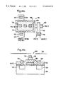
- FIG. 4 also, there is shown in schematic form a diagram of the MOSFET 116 .
- FIG. 4 a shows the MOSFET 116 in plan view and
- FIG. 4 b is a sectional view of the MOSFET 116 along a line IV—IV in FIG. 4 a .
- the MOSFET 116 has a source contact 120 and a drain contact 122 , each of which contact respective implant regions 124 and 126 in a n-type substrate 128 .
- the poly-silicon floating gate 118 is surrounded by an oxide region 130 .
- a poly-silicon control gate 132 with contacts 134 overlies the floating gate 118 .
- a poly-silicon tunnelling injector 136 In order to inject charge onto the floating gate 118 , a poly-silicon tunnelling injector 136 , having a contact 138 , overlies a limb 140 of the floating gate 118 . Charge is injected onto the floating gate 118 when a high voltage is applied to the injector 136 through an electron tunnelling process. The ability to alter the charge on the floating gate is required in order to trim the operation of the circuit 100 to reduce inter-pixel variations.
- An injector select line (not shown) is connected to the contact 138 and to contacts of other tunnelling injectors in the same row as the circuit 100 .
- the current-voltage characteristics arising from the tunnelling process mean that if a high voltage is applied to all the injectors within a row, the difference in floating gate potentials between the selected and de-selected devices must ensure that only the selected device will be programmed.
- the coupling of the select signal onto the floating gate distinguishes the selected device from the rest of the population. In consequence, changing the select signal between its two states should change the floating gate potential by at least three volts. If the select signal is either 0 V or 5 V, then the ratio of the capacitance of the control gate 132 capacitance to the total floating gate capacitance is at least 0.6.
- the diode connected MOSFETs 104 and 106 are operated in a sub-threshold regime.
- MOSFET device characteristics are described by S. M. Sze in “Physics of Semiconductor Devices”, John Wiley & Sons, New York, 1981, pages 431 to 510, where the term sub-threshold is explained.
- the response of the phototransistor 102 is, tailored, by for example controlling its size, so that the photocurrent generated at a maximum operating illumination level is not sufficient to drive the MOSFETs 104 and 106 above the subthreshold regime. It has been found that for a diode-connected load MOSFET operating in the sub-threshold regime that the input current, I in , is related to the gate-source potential, V gs , by the equation,
- equation (1) remains generally applicable and the output voltage is still a function of the logarithm of the photo-current.
- I is the source current and V T and ⁇ are device parameters.
- the floating gate MOSFET 116 provides a programmable current source within the pixel for trimming variations in both the variations of the parameters of the MOSFET 108 , V T and ⁇ , and variations in V in such as variations in the gain G of the phototransistor 102 or the device parameters of the MOSFETs 104 and 106 .
- the voltage applied to the select line 112 during the ultra-violet irradiation should be slightly greater than the normal maximum operating voltage, which is 5 V. If the voltage is set at 6 V, when the MOSFET 116 is de-selected, with the voltage on the line 112 being at 5 V, and a ratio of C pp /C tot equal to 0.6, the floating gate potential would be at approximately 5.4 V. When the MOSFET 116 is selected, the potential on the line 112 being 0 V, then the floating gate potential would be at 2.4 V, low enough to turn the device on. This initialisation process thus ensures that de-selected devices are turned off whilst only selected devices are turned on.
- each pixel circuit is trimmed to remove inter-pixel variations.
- the detector unit 52 of FIG. 2 is biased into its normal operating mode and a uniform illumination is applied to the detector array 54 .
- the output from each pixel is then compared to a desired output. If these two values are not within the required tolerance, then logic elements (not shown) switches a high voltage pulse onto the required injector select line. If the voltage on the floating gate 118 requires raising, the line 112 is set to 0 V and the high voltage pulse is switched onto the injector select line connected to the injector 136 .
- the floating gate potential on other devices in the same row are substantially unchanged since their respective select lines are set at 5 V.
- MOSFET 116 Increasing the potential on the floating gates of the MOSFETs such as MOSFET 116 has the effect of decreasing the current through the floating gate device and the output voltage placed on the row output line such as the row output line 110 will be reduced.
- the desired output voltage must therefore be lower than the lowest expected initial voltage after the initialisation process.
- Each pixel is programmed with several pulses until the output voltage is equal to the desired value.
- FIG. 5 there is shown a circuit 200 suitable for routing a high voltage pulse onto the injector select lines of the FIG. 3 circuit.
- the circuit 200 is described by J. R. Mann in “Floating-gate circuits in MOSIS”, Technical Report 824. Massachusetts Institute of Technology, Lincoln Laboratory, November 1990.
- the circuit 200 comprises two pairs of p-channel MOSFETs 202 to 208 connected in series. A positive high voltage signal is switched to an output line 210 by switching a low voltage input signal and its complement to respective n-channel MOSFETs 212 and 214 .
- the devices in the circuit 200 are configured so as to have an increased breakdown voltage compared with conventional MOSFETs. As described by Mann. low dose implants are used to modify the device drain structure.
- the circuit 200 provides 14.4 V pulses. This voltage will produce an estimated programming current of 0.2 pA. It is estimated that under these conditions, deselected floating gate MOSFETs receive a programming current of approximately 10 ⁇ 10 pA. If the high voltage pulse is applied for 10 ⁇ s, then with a total floating gate capacitance of 0.1 pF, each pulse causes a shift in the potential on the floating gate of 20 ⁇ V. If the initial offset error was 50 mV, two thousand five hundred pulses would be required to trim one pixel circuit.
- Bipolar detectors are suitable for use at low levels of illumination. However, above illumination levels of approximately 1 W/m 2 , corresponding to office lighting conditions, a bipolar device may create too much photocurrent and the load devices operate non-logarithmically. At illumination levels of 1 kW/m 2 , corresponding to bright sunlight, the load devices would operate in saturation rather than subthreshold.
- the phototransistor 102 may be replaced by a photodiode.
- a photodiode of area 10 ⁇ 10 m 2 generates a photocurrent of approximately 25 pA under an illumination level of 1 W/m 2 . If the photocurrent exceeds a maximum value of typically 100 nA, the exponential current voltage characteristic is no longer valid. For a 10 ⁇ 10 m 2 photodiode, this current corresponds to an illumination level of 1 kW/m 2 , equivalent to bright sunlight. Brighter illumination levels will lead to a non-logarithmic response though deviations from ideal will be gradual, and the upper limit is therefore a soft limit.
- the lowest usable illumination level is determined by the response speed of the detector.
- the gate voltages of the load devices must change to balance the current flow within the pixel. This response is delayed by capacitances within the pixel.
- Load devices of size 10 ⁇ m ⁇ 10 ⁇ m give a load capacitance of 200 fF. Assuming this capacitance C is discharged by the change in photocurrent ⁇ I p , resulting in a change in output voltage ⁇ V, the time constant ⁇ is approximately equal to C ⁇ V/ ⁇ I p .
- ⁇ V for a photodiode is approximately 1 mV, which under office lighting conditions gives a value of ⁇ of 0.16 ms which would be suitable for resampling the pixel at 50 Hz.
- a photocurrent of 25 fA could be expected with an associated time constant of 160 ms.
- a photodiode would thus respond too slowly under these lighting conditions.
- Bipolar phototransistors proved greater photocurrent and so are better suited to low light levels.
- a detector could be fitted with an automatic iris.
- photodetector and the associated load devices may be replaced with a photovoltaic device, such as that described by J. Mann in SPIE, Volume 1473, “Visual Information Processing: From Neurons to Chips”, (1991), pages 128 to 136.
- the bar filter unit 58 comprises fourteen columns of circuit elements such as a circuit element 220 and a single column of circuit elements such as a circuit element 222 . There are seven columns of circuit elements such as the element 220 on either side of the column of circuit elements such as the circuit element 222 . There is some commonality of components between the elements 220 and 222 .
- Each element 220 and 222 includes a buffer unit 230 .
- the buffer units 230 are part of a sample and hold arrangement for passing data across the bar filter unit 58 .
- Each element 220 and 222 include a transmission gate 232 and a capacitance 234 .
- the transmission gates 232 act as switches which can connect and disconnect an output from one buffer unit 230 from the capacitance 234 to its immediate right. Data is moved across a row by closing each transmission gate in turn starting from the right using a vertical control line (not shown) which controls all the equivalent transmission gates in each column. If a transmission gate is closed when all the others in the same row are open, the result will be to shift data across the array to the right.
- FIG. 7 shows a diagram of a buffer unit 230 at component level.
- the buffer unit is a standard transconductance amplifier having two well-connected p-channel MOSFETs 250 and 252 .
- a well-connected MOSFET is a MOSFET which has a substrate which is electrically connected to its source.
- the MOSFETs 250 and 252 are connected to form a source coupled pair.
- the gate of the MOSFET 252 is connected to an output 254 which itself is connected to the drain of the MOSFET 252 .
- the buffer unit 230 has two n-channel MOSFETs 256 and 258 , the gates of which are connected together.
- the MOSFET 256 is diode connected with the source and gate being connected together.
- a voltage at a node b 3 from a signal line (not shown) controls current flowing in to the buffer unit 230 through a p-channel MOSFET 260 .
- the elements 220 and 222 include respective averaging units 274 and 276 for calculating a local average response.
- the averaging units 274 and 276 are each a modified operational transconductance amplifier.
- the averaging units 274 and 276 are substantially similar but each averaging unit 276 includes an additional MOSFET 278 for providing an output.
- the filtered outputs from the central column of circuits 222 are connected to an output line 280 through respective transmission gates 282 .
- the output line 280 is in turn is connected to the FIG. 2 imaging unit output 66 .
- the averaging units 274 and 276 each have an output 284 which connects each unit to its four nearest neighbours.
- the outputs 284 pass through respective transmission gates 286 to biasing units 288 which allow current injected from an output 284 to spread between neighbouring units such that the voltage at which the current is injected represents a local average of the pixel voltages. For clarity of illustration, vertical connections between neighbouring biasing units 288 are not shown in FIG. 6 .
- FIG. 8 a shows an averaging unit 274 in component form.
- the unit 274 has two p-channel MOSFETs 380 and 382 which are biased by potentials at nodes b 1 and b 2 respectively.
- the MOSFETs 380 and 382 act as a constant current source 383 .
- the potentials at nodes b 1 and b 2 are created by a source (not shown) comprising a current generator connected to two diode connected MOSFETs, the potentials at b 1 and b 2 being the respective gate potentials of the two MOSFETs.
- the unit 274 receives an input voltage from the FIG. 6 capacitor 234 of the circuit element 220 or 222 immediately to its left in FIG. 6 on an input line 384 .
- the input line 384 is connected to the gate of a p-channel MOSFET 386 .
- the unit 274 has a second input device, a further p-channel MOSFET 388 .
- Both of the MOSFETs 386 and 388 are well-connected—that is, their substrate is connected to their source.
- the MOSFETs 386 and 388 are connected to form a source coupled pair with the constant current source 383 acting as a common source bias.
- N-channel floating gate MOSFETs 390 and 392 act as drain loads to the MOSFETs 386 and 388 . Connections between associated MOSFETs 386 / 390 and 388 / 392 are drain to drain.
- the sources of the MOSFETs 390 and 392 are connected to earth; their gates are connected together and they act in combination as a current mirror circuit.
- the common gate connection of the MOSFETs 390 and 392 is connected to the common drain connections of MOSFETs 386 and 390 through an n-channel MOSFET 394 .
- MOSFET 394 When the MOSFET 394 is conducting, it forms a diode connection to the MOSFET 390 , which is required for normal operation.
- the gate of the MOSFET 394 is connected to a programming rail 396 by a line 398 .
- a p-channel MOSFET 400 has its gate connected to the line 398 .
- the drain of the MOSFET 400 is connected to the drain of the MOSFET 394 and the gates of the MOSFETs 390 and 392 .
- the source of the MOSFET 400 is connected to a V high rail, not shown in FIG. 8 a but shown in FIG. 6 as a rail 402 .
- the output 284 of the averaging unit 274 is connected to the common drain connection of the MOSFETs 388 and 392 .
- the output 284 is also connected to the gate of MOSFET 388 .
- a p-channel MOSFET 406 has its gate connected to a first column feedback line 408 and its source and drain terminals are connected to the output 284 and to a source/drain terminal of an n-channel MOSFET 410 .
- the gate of the MOSFET 410 is connected to the programming rail 396 and its other source/drain terminal is connected to a second column feedback line 412 .
- the source/drain terminals of the MOSFETs 406 and 410 are not distinguished since the relative potentials on these terminals are not predictable.
- the constant current source 383 feeds a current I tail to a node 414 .
- the magnitude of I tail is such that the MOSFETs of the unit 274 operate in a sub-threshold regime, where the current through a device, I D , follows the relationship I D ⁇ I 0 e ⁇ V gs , where I 0 is a device dependent parameter.
- the current I tail is divided between the MOSFETs 386 and 388 in a ratio depending on their differential gate voltage. If the gate voltages are equal, the same current, I tail /2, flows through each device.
- the line 396 is at 5 V, and the MOSFET 394 is conducting.
- the current which flows through the MOSFET 390 equal to the current through the MOSFET 386 , is then equal to the current through the MOSFET 392 . If there is a voltage difference between the potentials on the gates of the MOSFETs 386 and 388 then current is either injected onto or received from the output 284 .
- the output 284 is connected to the outputs of immediately surrounding averaging units and so the effect of the averaging unit 274 is that if the voltage input on the line 384 is different form the local average input, a current flows and due to resistive effects the local average voltage changes to a certain degree, thereby updating the local average.
- the averaging unit 274 Whilst the above operation of the averaging unit 274 describes the normal operation of the unit, it is necessary to carry out a trimming operation in order to reduce the effect of variations in I 0 between devices within the unit.
- the trimming operation the potentials on the floating gates of the floating gate MOSFETs 390 and 392 are adjusted.
- an initialisation step residual random charge on the floating gate devices is removed by exposing the device to ultra-violet radiation.
- the floating gate bar filter unit 58 is fabricated with a metal shield layer covering most of the circuits; the shield layer having a window above an area where the control gate overlaps the floating gate. The shield layer also protects the circuit from visible light during normal operation.
- the window is placed at the source end of the floating gate.
- the initialisation process is only required to achieve approximate equality between the potentials of the two floating gates.
- the line 396 is held at 5 V in order to allow the MOSFET 394 to conduct and the unit 274 to operate normally.
- the unit 274 may be trimmed to counteract device variations.
- a known constant signal chosen to represent a typical signal input and perhaps 2.5 V, is fed into the sample and hold circuits comprising the buffer units 230 , the transmission gates 232 and the capacitances 234 and therefore consequently to the input line 384 .
- the constant signal is supplied from an on-chip voltage source (not shown) and is connected to the bar filter unit 58 through transmission gates (not shown) which selectively connect either the signals from the detector unit 52 during normal operation or the constant signal during trimming operation. This arrangement enables the trimming of the detector unit 52 and the bar filter unit 58 to be carried out in parallel.
- the units 274 are trimmed one row after another.
- the row containing the units 274 which are to be trimmed is selected by setting the appropriate line 396 high and all other equivalent lines in the unit 58 low.
- a global control signal (not shown) is sent to all the transmission gates 286 in FIG. 6 to disconnect all the units 274 from other similar units.
- the line 412 is then set to the same voltage as the signal on the input line 384 and the line 408 is set low.
- the MOSFETs 406 and 410 are then conducting. Current flowing in the line 412 is then the output current when the two input voltages to the unit 274 are equal and is monitored.
- a double comparator arrangement shown in FIG. 9 may be used to determine whether the output current should be either increased, decreased, or if approximately zero remain unchanged.
- a double comparator arrangement is described in FR-A-2 543 363.
- the current may be changed by putting a high voltage pulse on either or both of respective programming lines for the floating gate MOSFETs 390 and 392 .
- These programming lines are indicated as vertical lines p 1 and p 2 respectively connected to units 274 within a column in FIG. 6 but are omitted from FIG. 8 a for clarity.
- the high voltage pulses are supplied by a circuit similar to the circuit 200 shown in FIG. 5, one of which is connected to each programming line.
- the line 396 is low and the unit 274 is therefore isolated and the channel of the MOSFET 400 is conducting rather than the MOSFET 394 .
- the voltage V high is then capacitively coupled through onto the floating gates of MOSFETs 390 and 392 .
- the voltage change induced on the floating gates of MOSFETs of deselected units must be at least 3 V. This may be controlled by having a large control-gate to floating-gate coupling capacitance or by using the largest possible value of V high , which saves circuit area.
- the voltage which is applied to the line 396 must be at least as high as the voltage V high applied to the source of MOSFET 400 .
- the averaging unit 276 is essentially similar to the averaging units 274 , the only difference being that the gate of the output MOSFET 278 is connected to the connection between floating gate devices 424 and 426 equivalent to the MOSFETs 390 and 392 of the unit 274 .
- the MOSFET 278 is a n-channel floating gate MOSFET.
- the MOSFET 278 is sensitive to any difference between the two input voltages.
- the gate voltage on the MOSFET 278 controls the flow of current through the device.
- each averaging unit 276 is selectably connected to the output line 280 by respective transmission gates 282 , each of which is controlled by a respective control signal on a control line Select o (not shown).
- the outputs from averaging units 276 of successive rows are consecutively coupled to the output line 280 .
- the floating gate devices 424 and 426 of the unit 276 are programmable to trim the operation of the unit 276 .
- the trimming operation for the unit 276 is the same as for the units 274 with a further step of programming the operation of the MOSFET 278 .
- the respective control line Select o is connected to the respective line 396 to ensure that the correct output device is monitored on the output line 280 .
- the output current from the MOSFET 278 is adjusted by varying the potential on its floating gate so that a pre-determined output current is obtained for zero differential input.
- the floating gate of the MOSFET 278 is programmed by the application of a high voltage on a programming line p 3 .
- a current measuring unit 442 measures the current flowing on the line 412 and outputs a signal on a line 444 in response to the measured current.
- the signal on the line 444 has a value (2.5 ⁇ ) volts, where ⁇ is dependent on the magnitude of the current. Thus if the current requires increasing, the signal is less than 2.5 V and if the current requires decreasing, the signal is greater than 2.5 V.
- the line 444 provides an input 446 to a comparator 448 and an input 450 to a comparator 452 .
- a second input 454 to the comparator 448 carries a voltage V 1 and a second input 456 to the comparator 452 carries a voltage V 2 .
- V 1 is slightly less than 2.5 V, perhaps 2.4 V
- V 2 is slightly greater than 2.5 V, perhaps 2.6 V. Altering the values of V 1 and V 2 affects the precision of the trimming process. The exact values would be determined by routine testing, balancing the speed of the trimming operation against the degree of precision. The differences between 2.5 V and the values of V 1 and V 2 provide an acceptable range for the current on line 412 .
- the comparator 448 generates a logical ‘1’ on an output 458 when the signal on the line 444 is less than V 1 and a logical ‘0’ when it is greater; similarly the comparator 452 generates a logical ‘1’ on an output 460 when the signal on the line 444 is greater than V 2 and a logical ‘0’ when it is less.
- the outputs 458 and 460 provide the inputs for a NOR gate 462 .
- the NOR gate 462 provides a signal to a pulse generator 464 when the output current on the line 412 is within a desired range and hence the trimming operation for a pair of MOSFETs within an averaging unit is complete.
- the pulse generator 464 generates a series of pulses during the trimming operation. These pulses are output to two AND gates 466 and 468 .
- the AND gate 466 carries out a logical AND operation on the pulsed output of the pulse generator 464 and the output of the comparator 448 , resulting in a signal S 1 .
- the AND gate 468 carries out a logical AND operation on the pulsed output of the pulse generator 464 and the output of the comparator 452 , resulting in a signal S 2 .
- the signal S 1 controls switches (not shown) which switch the low voltage input signals to a high voltage pulse routing circuit (not shown) as shown in FIG. 5 which provides a pulse on the programming line p 1 to program MOSFETs 390 or 424 as appropriate.
- the signal S 2 controls switches (not shown) which switch low voltage input signals to a further high voltage routing circuit (not shown) which provides a pulse on the programming line p 2 to program MOSFETs 392 or 426 as appropriate.
- a pulse is thus only sent to a respective one of the pair of floating gate MOSFETs of the averaging units when either of the comparators 448 and 452 generates a logical ‘1’, indicating that further adjustment of the current on the line 412 is required.
- a pulse cannot be sent to both MOSFETs of an averaging unit simultaneously.
- the potential of the floating gate of the MOSFETs 390 or 424 are increased if the current in the line 412 requires increasing and the potential of the floating gate of the MOSFETs 392 or 426 are increased if the current in the line 412 requires reducing.
- the pulse generator 464 receives a signal from the NOR gate that the trimming of a particular averaging unit is complete, the trimming of the next averaging unit is initiated by a signal sent to a logic unit (not shown) which controls the setting of the lines 396 .
- the biasing unit 288 comprises a bias circuit 490 and an arrangement of lateral connections 492 .
- the bias circuit 490 comprises two p-channel MOSFETs 500 and 502 and two n-channel MOSFETs 504 and 506 .
- the drains of the MOSFETs 500 and 502 are connected together and connected to the drain of an n-channel MOSFET 508 .
- the gates of the MOSFETs 504 and 506 are linked together.
- the gate of the MOSFET 500 is connected by an input line 510 to an output 512 of a transmission gate 286 .
- the MOSFET 502 is diode connected.
- a further diode connected p-channel MOSFET 514 is positioned between the MOSFETs 502 and 506 .
- the arrangement of lateral connections 492 comprises four p-channel MOSFETs 516 to 522 .
- the gate of the MOSFET 514 is connected to the gates of the four p-channel MOSFETs 516 to 522 .
- One of the source/drain contacts of each MOSFET 516 to 522 is connected to the output 512 and the other source/drain contact of each MOSFET is connected to a respective output to a neighbouring biasing unit.
- the conductance of the bias circuit 490 is controlled by in input voltage V R applied to the gate of the MOSFET 508 .
- V R input voltage
- the voltage generated by the input decreases as a function of distance from the input because some of the current injected by the input is shunted to ground.
- V n ⁇ n V 0 ,
- L is a characteristic length, or diffusion length, such that 1/L is equal to ⁇ square root over (RG) ⁇ .
- the input voltage V R to the bias circuit 490 controls the conductance to ground of the resistive bias circuit. Changing V R thus changes the characteristic length L of the filter. Simulation results show that characteristic length of two for a filter with fifteen columns performs well, and a characteristic length of four behaves acceptably.
- the imaging unit 50 has been described as including an array 54 of 512 ⁇ 512 pixels.
- the averaging process performed by the bar filter unit 58 is such that a filtered output is not obtainable for pixels in a border region of the array 54 .
- the bar filter unit 58 comprises fifteen columns of circuit elements 220 and 222 , with the circuit elements 222 forming a central column, data from the first seven columns of the array 54 are passed across the bar filter unit 58 with no output from the central column being measured. Only when the bar filter unit 58 is filled are outputs taken from the central column. Likewise, no output is measured from the last seven columns of the array 54 . There will also be pixels from top and bottom of the array 54 which do not contribute to a final image.
- the amplifier 600 comprises four MOSFETs M 1 , M 2 , M 3 , and M 4 .
- the MOSFETs M 1 and M 2 are p-channel and the MOSFETs M 3 and M 4 are n-channel.
- I 0 variations will cause errors in the differential input voltage, ⁇ V in and the size of the output current.
- the size of the injected current for a particular differential input voltage determines the extent over which the average response is calculated and is therefore equivalent to errors in the biasing units 288 , which are considered to be negligible. This source of errors will therefore also be negligible. Simulations suggest that it is the errors ⁇ V in which are equivalent to errors in the signal representing the scene, which must be minimised.
- I 0,M3 or I 0,M4 Changing the charge on a floating-gate device when the channel is biased to operate subthreshold, is equivalent to varying the I 0 parameter.
- I o variations changing the input devices M 1 and M 2 to floating gate devices will reduce the channel conductance g m of these devices and therefore the circuit gain. Therefore, changing the load devices to floating gate devices should be considered.
- Replacing the MOSFETs M 3 and M 4 in the current mirror by floating-gate devices will create the flexibility required to ensure that a zero differential input leads to a zero output current.
- increasing I 0,M3 will increase I M4 whilst increasing I 0,M4 will decrease I M4 .
- the two floating-gate devices can be used in conjunction with a single polarity high-voltage programming voltage to trim a circuit to remove the random variations.
- I ds I 0 exp( ⁇ V gb /U T )[exp( ⁇ V sb /V T ) ⁇ exp( ⁇ V db /V T )].
- V gb will vary with the common-mode input voltage variations in ⁇ , ⁇ , will create an effective I 0 , I′ 0 , where
- I′ 0 I 0 exp( ⁇ V gb /U T )
- the imaging system 50 of FIG. 2 may be incorporated within a surveillance system.
- a surveillance system 650 comprises an imaging system 660 and a display system 662 .
- the imaging system 660 is similar to the imaging system 50 .
- Image signals from successive pixels within a column and from successive columns are passed from the imaging system 660 to the display system 662 along a data line 664 .
- the signals from the imaging system 660 control the intensities of display pixels (not shown) within the display system 662 in a manner familiar to those knowledgeable about display technologies.
- the surveillance system 650 provides advantages over prior systems in that the degree to which local illumination determines the appearance of an object within a scene is reduced.
- a conventional video camera based system if there are regions of intense brightness within an overall dark scene, then the automatic gain control on the camera will result in objects within the dark background becoming indiscernible.
- Such a scenario might be at night when the brightness of an approaching car's headlights render all surrounding information indiscernible.
- Another possible scenario might be a surveillance camera in a city at night where, as a result of locally intense street lighting, objects in shadow are hidden.
- the number of bits which describe the pixel intensity may be selected according to the quality of image required. In certain situations, it might be desirable for an image to be represented by one bit per pixel. Whilst for a standard image, the quality deteriorates rapidly as the number of bits is reduced, the image quality of an image generated by the system 660 degrades gracefully as the number of bits is reduced. Even with a one bit per pixel representation, images are recognisable since edges present in a scene are preserved.
- the imaging system 50 represents a fully integrated system in which the logarithmic response and the spatial filtering are achieved on a single integrated circuit. Integrating the system 50 on a single integrated circuit provides advantages in terms of compactness and power consumption. Other surveillance systems incorporating means for generating a logarithmic response to incident radiation and subsequent spatial filtering may be constructed.
- an imaging system 700 comprising a detector array 710 , a signal digitiser 712 and a digital processor 714 .
- the detector array comprises an array of photodetectors 716 .
- the photodetectors 716 may be photo-transistors or photo-diodes with a select device to allow the current from each pixel within a column to be selectively connected to an output 718 which is common to each row. Connecting the small photo-currents to the relatively large capacitances which arise from using a common row output may limit the speed of operation of the array. This can be avoided by using a buffer which holds the output line at a constant voltage.
- any unselected devices can be connected to a second common line which is held at the same voltage.
- a second common line which is held at the same voltage.
- the signals from the array 710 are passed to the digitiser 712 .
- the digitiser 712 In order to be able to detect intensity changes at a level of 1%, the maximum sensitivity of the eye, over an intensity range of three decades, the digitiser 712 would need to be capable of digitising signals from the photodetectors at an accuracy of approximately 17 bits per pixel. This figure of 17 is determined from the expression: log 2 ⁇ ( 10 3 0.01 ) ⁇ 17.
- the digitiser 712 may incorporate analogue to digital converters produced by Analog Devices in their series AD9022/AD9026 which are advertised as being capable of 12-bit conversion at over 20 MHz.
- the digitised signals are passed to the processor 714 .
- the processor 714 calculates the logarithm of the digitised signals and performs a high pass filtering operation on the result.
- the high pass filtering may be achieved in the spatial domain by performing a convolution operation with a suitable kernel familiar to those skilled in image processing.
- the processor 714 sends signals to a display unit 716 which processes the signals from the processor 714 and displays the resulting image.
- the number of bits representing the final image may be selected according to the clarity of image required and other considerations such as possible image recognition algorithms or data storage and/or transmission requirements.
- the system 700 with its linear representation suffers from the disadvantage that bright features will be represented too accurately whilst low brightness features will not be represented accurately enough. This disadvantage may be overcome by obtaining an analogue logarithmic representation prior to digitisation.
- the number of bits required in a digitised signal to represent a 1% change in intensity over an intensity range of three decades is reduced to approximately I 0 as determined from the expression: log 2 ⁇ ( ln ⁇ ( 10 3 ) ln ⁇ ( 1.01 ) ) ⁇ 10.
- An approach for obtaining a logarithmic representation is to include a logarithmic current-sense amplifier before the output 718 .
- a logarithmic current-sense amplifier before the output 718 .
- a non-uniformity correction step will therefore be required after digitisation in order to prevent these variations from obscuring the fine details within a scene.
- Such a non-uniformity correction step could be performed by the processor 714 prior to the calculation of the logarithmic response by multiplying the digitised signal from each pixel by a scaling factor determined in a calibration routine, or more accurately multiplying the signal by an interpolated correction factor determined using a series of calibration values obtained over a range of illumination levels.
- the correction could be achieved by subtracting a correction value after the logarithmic response has been calculated.
- Mead and Delbschreib suggest that it would be difficult to operate a large array at the frame rate for low photo-currents of possibly 10 pA, expected at low illumination levels.
- One of the major problems is the need to prevent “ringing”.
- One approach to overcome this is to employ “smart” sensor concepts which predict the final output from a ringing signal without waiting for the ringing to stop.
- a further approach is to replace the voltage mode buffer circuit described by Mead and Delbschreib with a current mode buffer circuit which holds the output node at a fixed voltage. Without these solutions, the system may be limited to small arrays operating at illumination levels which produce nanoamp photocurrents.
- FIG. 14 shows a current mode buffer circuit 750 for achieving a solution to this problem.
- the circuit 750 comprises six p-channel MOSFETs 752 to 762 and three n-channel MOSFETs 764 to 768 .
- MOSFETs 752 , 754 , and 756 are matched MOSFETs, as are MOSFETs 764 , 766 , and 768 , and MOSFET pair 760 and 762 .
- the detector array 710 is connected to a node 770 , to provide an input current, I in .
- the symmetry of the layout of MOSFETs 760 and 766 mean that the node 770 is held at a constant voltage determined by a voltage source V in .
- the load capacitance for changes in the input current are the capacitances associated with the current mirrors formed by MOSFETs 764 , 766 , and 768 .
- a bias current I bias is added to the input current I in from MOSFET 754 .
- This bias current is generated by attaching a current sink to MOSFET 752 .
- the summed current I in +I bias is copied into MOSFET 768 .
- MOSFET 756 then supplies current I bias so that the current which flows through MOSFET 758 is I in .
- MOSFET 758 which is diode-connected.
- MOSFETs 756 and 768 may be replaced by several MOSFETs which are the same as MOSFETs 752 and 764 respectively. If n MOSFETs are used in parallel in these positions, then the circuit will operate n-times faster.
- a current-voltage conversion may be performed within the pixel, followed by a buffer circuit such as a source-follower.
- the current to voltage conversion should create a voltage which is proportional to the logarithm of the photo-current in order to avoid the previously discussed problems of a linear representation.
- Such a conversion may be achieved using diode connected load MOSFETs operating in the sub-threshold regime.
- the photodetectors 716 of the array 710 may be replaced by logarithmic photodetector circuits such as the receptor unit 20 of FIG. 1 .
- non-uniformity corrections to the outputs of the logarithmic photodetector circuits could be performed after digitisation
- the result of performing non-uniformity correction digitally would be to produce a corrected output which would be accurate to one less bit than the uncorrected input. This may be avoided by implementing non-uniformity correction within the detector array.
- Such a system would include an array of photodetectors similar to the array 54 of the imaging unit 50 of FIG. 2 . Instead of the output being passed to an analogue filter unit, the output of the array could be digitised and the resulting digital signals filtered in the spatial domain using a convolution process. In cost-sensitive markets, the digitiser accuracy is often reduced to a minimum in order to cut costs. On-chip non-uniformity correction would give a factor of 2 more dynamic range for a given digitiser accuracy.
- the filtering operation in the spatial domain may be filter operation using a ⁇ -Gaussian filter.
- a general kernel operating on a 512 ⁇ 512 image at 50 Hz would require a digital processor capable of approximately 512 2 ⁇ 15 2 ⁇ 50, or 3 ⁇ 10 9 , multiplication and addition operations per second.
- the separability of the Gaussian kernel into horizontal and vertical parts means that the 15 ⁇ 15 kernel can be replaced by two 15 ⁇ 1 kernels, requiring only 512 2 ⁇ 2 ⁇ 15 ⁇ 50, or 4 ⁇ 10 8 , multiplication and addition operations per second.
- the resulting image must be subtracted from the original logarithmic image suitably normalised.
- Using the 1-dimensional filters is nearly an order of magnitude less computationally expensive than using a 2-dimensional filter. This results in a reduction in the required system performance, and so leads to a simpler architecture.
- a plan of the convolution filter architecture for a 1-dimensional filter is shown in FIG. 15 .
- Analogue spatial filtering of a corrected logarithmic detector output may be achieved using an averaging unit similar to the lateral averaging unit 22 of the FIG. 1 system. This would consume less power than the digital alternatives and may be cheaper for manufacture in large numbers.
- the fully integrated system 660 would be the most compact and reliable system and may consume less power, important for battery operated systems.
- Imaging systems such as those described above which incorporate a logarithmic representation of a scene which has undergone a high-pass filter operation would be suitable for use in surveillance systems. Such systems would be particularly useful for imaging natural scenes where there is a wide variation in illumination levels, such as regions in shadow and regions in bright sunlight.
- Logarithmic detectors and high-pass spatial filters may be combined to produce a contrast encoded, edge-enhanced representation of a visual scene.
- FIG. 16 there is shown a simulation of a representation of a village scene before and after filtering.
- FIG. 16 a shows an image which would have been obtained with a conventional imaging system, for example a video camera.
- FIG. 16 b shows the same image after logarithmic conversion and spatial filtering.
- FIG. 17 shows a representation of a road scene before and after filtering.
- FIG. 17 a shows an image which would have been obtained from a conventional imaging system and
- FIG. 17 b shows the same image after logarithmic conversion and spatial filtering.
- 16 b and 17 b were obtained from a linear detector and were subjected to digital processing in a manner similar to that described with reference to the system 700 of FIG. 13, with a difference being that the images were captured using a CCD camera.
- the edge around the filtered image in FIG. 16 b arises because the convolution operation results in an image which is smaller than the input.
- the filter operation used to produce the filtered images shown in FIGS. 16 b and 17 b had a ⁇ n value of two.
- FIG. 18 shows in graphical form the distribution of the pixel intensity values of the FIG. 16 and FIG. 17 images.
- FIG. 18 a shows the distribution of intensity values in the filtered outputs.
- a solid line 800 is a plot of the pixel intensity distribution from FIG. 16 b and a solid line 802 is a plot of the pixel intensity distribution from FIG. 17 b .
- FIG. 18 b shows the distribution of intensity values in the filtered outputs.
- a solid line 804 is a plot of the pixel intensity distribution from FIG. 16 a and a solid line 806 is a plot of the pixel intensity distribution from FIG. 17 a . Comparing FIG. 18 a with FIG. 18 b , the distributions in intensities in FIG. 18 a is considerably narrower than those in FIG.
- FIG. 18 b The distribution intensities in FIG. 18 a show a uni-modal distribution centred around a particular intensity. Since the distributions in FIG. 18 a are narrower than those in FIG. 18 b , it follows that the image can be represented in fewer bits. Analysis of FIG. 18 a indicates that FIGS. 16 b and 17 b could be represented using as few as five bits per pixel.
- FIG. 19 shows the images of FIG. 16 digitised so as to be represented by three bits per pixel.
- FIG. 19 a represents a digitisation of FIG. 16 a and
- FIG. 19 b represents a filtered output.
- FIG. 20 is a representation of the FIG. 16 image in which, after a threshold has been imposed, the image is represented by a single bit per pixel. Such a representation still contains recognisable detail and may be a suitable format for image recognition algorithms to operate on, as well as reducing the amount of data which a data storage system would have to store.
- FIG. 21 is a simulation of the response of a conventional imaging system when imaging a car at night. As can be seen from FIG. 21, the effect of the car's headlights is to cause the obliteration of most of the detail of the car.
- FIG. 22 is a simulation of the same image which would be produced by an imaging system comprising a logarithmic detector and a spatial filter.
- FIG. 23 is a simulation of the same image in which a linear current-mode detector is used to capture the image and after digital processing to filter the image spatially. In the spatial filter, a local estimate of the additional photons from the headlights is subtracted from the response of each pixel.
- a system for obtaining the image of FIG. 23 would comprise a high-dynamic range detector array together with a high dynamic range digitiser and a digital processor; in other words, similar to the system 700 without the logarithmic conversion.
- FIGS. 21 to 23 are simulations of night-time scenes, it may be seen that such a system would be capable of identifying important features, such as a car's registration identity, without being dazzled.
- a further possible application for imaging systems comprising a logarithmic response photodetector and filtering means is in an electronic photographic system.
- Currently available electronic cameras rely on a combination of limited resolution, limited picture storage capability and image compression techniques to achieve a realistic performance.
- An electronic photographic system which generated a logarithmic representation of an image and filtered the image would have a lower data storage requirement, which would be of benefit in increasing the number of pictures which could be stored, or the resolution, or both.
- the logarithmic representation of the image Prior to the display of images stored by such a system, the logarithmic representation of the image could be converted back to a linear representation for either displaying on a screen or for printing using a standard printer.
- power consumption would be of critical importance and so the system 50 might be the most suitable for incorporation into such a camera.
Abstract
Description


Claims (40)


Applications Claiming Priority (1)
| Application Number | Priority Date | Filing Date | Title |
|---|---|---|---|
| PCT/GB1995/002808 WO1997021304A1 (en) | 1995-12-01 | 1995-12-01 | Imaging system |
Publications (1)
| Publication Number | Publication Date |
|---|---|
| US6683645B1 true US6683645B1 (en) | 2004-01-27 |
Family
ID=10769537
Family Applications (1)
| Application Number | Title | Priority Date | Filing Date |
|---|---|---|---|
| US09/068,887 Expired - Lifetime US6683645B1 (en) | 1995-12-01 | 1995-12-01 | Imaging system with low sensitivity to variation in scene illumination |
Country Status (3)
| Country | Link |
|---|---|
| US (1) | US6683645B1 (en) |
| JP (1) | JP4036896B2 (en) |
| DE (1) | DE69528386T2 (en) |
Cited By (35)
| Publication number | Priority date | Publication date | Assignee | Title |
|---|---|---|---|---|
| US20010052940A1 (en) * | 2000-02-01 | 2001-12-20 | Yoshio Hagihara | Solid-state image-sensing device |
| US20020021121A1 (en) * | 2000-07-19 | 2002-02-21 | Satoshi Nakamura | Solid-state image sensing apparatus |
| US20020177895A1 (en) * | 1999-05-07 | 2002-11-28 | Wilfried Nisch | Retina implant |
| US6950137B1 (en) * | 1999-03-16 | 2005-09-27 | Nec Corporation | Noise reduction circuit for charge coupled imaging device |
| WO2007028001A2 (en) * | 2005-08-30 | 2007-03-08 | Georgia Tech Research Corporation | Method and device for performing offset cancellation in an amplifier using floating-gate transistors |
| US7269359B1 (en) * | 2002-12-18 | 2007-09-11 | Itt Manufacturing Enterprises, Inc. | Focal plane array with synchronous detection circuits for an active remote sensing system |
| WO2008091024A2 (en) * | 2007-01-26 | 2008-07-31 | Nec Display Solutions, Ltd. | Image quality improving apparatus and image quality improving method |
| US20080316151A1 (en) * | 2003-05-19 | 2008-12-25 | Seiko Epson Corporation | Electro-optical apparatus and method of driving the electro-optical apparatus |
| US20090296814A1 (en) * | 2008-05-28 | 2009-12-03 | Cyberlink Corp. | Determing an intermediate image |
| US20100329558A1 (en) * | 2003-02-27 | 2010-12-30 | Saquib Suhail S | Digital image exposure correction |
| US20110172736A1 (en) * | 2010-01-14 | 2011-07-14 | Nano-Retina, Inc. | Penetrating electrodes for retinal stimulation |
| EP2400547A1 (en) * | 2009-02-18 | 2011-12-28 | Nanjing University | Photosensitive detector with composite dielectric gate mosfet and singal reading method thereof |
| US8428740B2 (en) | 2010-08-06 | 2013-04-23 | Nano-Retina, Inc. | Retinal prosthesis techniques |
| US8442641B2 (en) | 2010-08-06 | 2013-05-14 | Nano-Retina, Inc. | Retinal prosthesis techniques |
| US8571669B2 (en) | 2011-02-24 | 2013-10-29 | Nano-Retina, Inc. | Retinal prosthesis with efficient processing circuits |
| US8706243B2 (en) | 2009-02-09 | 2014-04-22 | Rainbow Medical Ltd. | Retinal prosthesis techniques |
| US20150350495A1 (en) * | 2012-01-31 | 2015-12-03 | Prime Image Delaware, Inc. | Detecting a vertical cut in a video signal for the purpose of time alteration |
| US9265945B2 (en) | 2009-02-09 | 2016-02-23 | Nano-Retina, Inc. | Retinal prosthesis |
| US9331791B2 (en) | 2014-01-21 | 2016-05-03 | Nano Retina Ltd. | Transfer of power and data |
| US9370417B2 (en) | 2013-03-14 | 2016-06-21 | Nano-Retina, Inc. | Foveated retinal prosthesis |
| CN105723700A (en) * | 2013-09-11 | 2016-06-29 | 瓦里安医疗系统公司 | Pixel circuit with constant voltage biased photodiode and related imaging method |
| US9474902B2 (en) | 2013-12-31 | 2016-10-25 | Nano Retina Ltd. | Wearable apparatus for delivery of power to a retinal prosthesis |
| US10720217B1 (en) | 2019-01-29 | 2020-07-21 | Silicon Storage Technology, Inc. | Memory device and method for varying program state separation based upon frequency of use |
| US10748630B2 (en) | 2017-11-29 | 2020-08-18 | Silicon Storage Technology, Inc. | High precision and highly efficient tuning mechanisms and algorithms for analog neuromorphic memory in artificial neural networks |
| US10803943B2 (en) | 2017-11-29 | 2020-10-13 | Silicon Storage Technology, Inc. | Neural network classifier using array of four-gate non-volatile memory cells |
| US11064142B1 (en) | 2013-09-11 | 2021-07-13 | Varex Imaging Corporation | Imaging system with a digital conversion circuit for generating a digital correlated signal sample and related imaging method |
| US11087207B2 (en) | 2018-03-14 | 2021-08-10 | Silicon Storage Technology, Inc. | Decoders for analog neural memory in deep learning artificial neural network |
| US11270763B2 (en) | 2019-01-18 | 2022-03-08 | Silicon Storage Technology, Inc. | Neural network classifier using array of three-gate non-volatile memory cells |
| US11276132B2 (en) | 2020-01-30 | 2022-03-15 | Samsung Electronics Co., Ltd. | Data processing method and sensor device for performing the same |
| US11308383B2 (en) | 2016-05-17 | 2022-04-19 | Silicon Storage Technology, Inc. | Deep learning neural network classifier using non-volatile memory array |
| US11409352B2 (en) | 2019-01-18 | 2022-08-09 | Silicon Storage Technology, Inc. | Power management for an analog neural memory in a deep learning artificial neural network |
| US11423979B2 (en) | 2019-04-29 | 2022-08-23 | Silicon Storage Technology, Inc. | Decoding system and physical layout for analog neural memory in deep learning artificial neural network |
| US11544349B2 (en) | 2019-01-25 | 2023-01-03 | Microsemi Soc Corp. | Method for combining analog neural net with FPGA routing in a monolithic integrated circuit |
| US11893478B2 (en) | 2019-01-18 | 2024-02-06 | Silicon Storage Technology, Inc. | Programmable output blocks for analog neural memory in a deep learning artificial neural network |
| US11972795B2 (en) | 2023-03-10 | 2024-04-30 | Silicon Storage Technology, Inc. | Verification of a weight stored in a non-volatile memory cell in a neural network following a programming operation |
Families Citing this family (2)
| Publication number | Priority date | Publication date | Assignee | Title |
|---|---|---|---|---|
| JP4545978B2 (en) * | 2001-03-28 | 2010-09-15 | キヤノン株式会社 | Image processing apparatus and image input apparatus |
| JP2020188386A (en) * | 2019-05-15 | 2020-11-19 | ソニーセミコンダクタソリューションズ株式会社 | Solid-state imaging apparatus and electronic apparatus |
Citations (13)
| Publication number | Priority date | Publication date | Assignee | Title |
|---|---|---|---|---|
| US4667239A (en) * | 1984-08-06 | 1987-05-19 | Texas Instruments Incorporated | Signal peaking device for single-line video input |
| US4719350A (en) | 1986-01-30 | 1988-01-12 | Hughes Aircraft Co. | Radiation imaging enhancement |
| US4780762A (en) | 1985-12-04 | 1988-10-25 | Olympus Optical Co., Ltd. | Image signal correcting circuit |
| US4973833A (en) | 1988-09-28 | 1990-11-27 | Minolta Camera Kabushiki Kaisha | Image sensor including logarithmic converters |
| US5153731A (en) | 1989-12-18 | 1992-10-06 | Olympus Optical Co., Ltd. | Solid state image pick-up device and apparatus capable of providing filtering output with direct and real time manner |
| US5343254A (en) * | 1991-04-25 | 1994-08-30 | Olympus Optical Co., Ltd. | Image signal processing device capable of suppressing nonuniformity of illumination |
| EP0626784A1 (en) | 1993-05-28 | 1994-11-30 | Canon Kabushiki Kaisha | Gain-controlled solid-state image pickup device |
| US5557234A (en) * | 1992-02-27 | 1996-09-17 | The Secretary Of State For Defence In Her Britannic Majesty's Government Of The United Kingdom Of Great Britain And Northern Ireland | Differential amplifier with mismatch correction using floating gates |
| US5808676A (en) | 1995-01-03 | 1998-09-15 | Xerox Corporation | Pixel cells having integrated analog memories and arrays thereof |
| US5977535A (en) * | 1992-09-30 | 1999-11-02 | Lsi Logic Corporation | Light sensing device having an array of photosensitive elements coincident with an array of lens formed on an optically transmissive material |
| US6014685A (en) * | 1994-05-05 | 2000-01-11 | The Secretary Of State For Defence In Her Britannic Majesty's Government Of The United Kingdom Of Great Britain And Northern Ireland | Electronic circuit for determination of distances between reference and data points |
| US6058223A (en) * | 1996-06-27 | 2000-05-02 | The Johns Hopkins University | Video-centroid integrated circuit |
| US6212289B1 (en) * | 1995-04-07 | 2001-04-03 | California Instititute Of Technology | Pulse domain neuromorphic integrated circuit for computing motion |
-
1995
- 1995-12-01 JP JP52104697A patent/JP4036896B2/en not_active Expired - Fee Related
- 1995-12-01 US US09/068,887 patent/US6683645B1/en not_active Expired - Lifetime
- 1995-12-01 DE DE69528386T patent/DE69528386T2/en not_active Expired - Fee Related
Patent Citations (13)
| Publication number | Priority date | Publication date | Assignee | Title |
|---|---|---|---|---|
| US4667239A (en) * | 1984-08-06 | 1987-05-19 | Texas Instruments Incorporated | Signal peaking device for single-line video input |
| US4780762A (en) | 1985-12-04 | 1988-10-25 | Olympus Optical Co., Ltd. | Image signal correcting circuit |
| US4719350A (en) | 1986-01-30 | 1988-01-12 | Hughes Aircraft Co. | Radiation imaging enhancement |
| US4973833A (en) | 1988-09-28 | 1990-11-27 | Minolta Camera Kabushiki Kaisha | Image sensor including logarithmic converters |
| US5153731A (en) | 1989-12-18 | 1992-10-06 | Olympus Optical Co., Ltd. | Solid state image pick-up device and apparatus capable of providing filtering output with direct and real time manner |
| US5343254A (en) * | 1991-04-25 | 1994-08-30 | Olympus Optical Co., Ltd. | Image signal processing device capable of suppressing nonuniformity of illumination |
| US5557234A (en) * | 1992-02-27 | 1996-09-17 | The Secretary Of State For Defence In Her Britannic Majesty's Government Of The United Kingdom Of Great Britain And Northern Ireland | Differential amplifier with mismatch correction using floating gates |
| US5977535A (en) * | 1992-09-30 | 1999-11-02 | Lsi Logic Corporation | Light sensing device having an array of photosensitive elements coincident with an array of lens formed on an optically transmissive material |
| EP0626784A1 (en) | 1993-05-28 | 1994-11-30 | Canon Kabushiki Kaisha | Gain-controlled solid-state image pickup device |
| US6014685A (en) * | 1994-05-05 | 2000-01-11 | The Secretary Of State For Defence In Her Britannic Majesty's Government Of The United Kingdom Of Great Britain And Northern Ireland | Electronic circuit for determination of distances between reference and data points |
| US5808676A (en) | 1995-01-03 | 1998-09-15 | Xerox Corporation | Pixel cells having integrated analog memories and arrays thereof |
| US6212289B1 (en) * | 1995-04-07 | 2001-04-03 | California Instititute Of Technology | Pulse domain neuromorphic integrated circuit for computing motion |
| US6058223A (en) * | 1996-06-27 | 2000-05-02 | The Johns Hopkins University | Video-centroid integrated circuit |
Non-Patent Citations (2)
| Title |
|---|
| IEE Colloquium on 'Integrated Imaging Sensors and Processing', Dec. 5, 1994, London, UK, pp. 1-6, XP000575379 S. Collins et al.: "A Critical Review of analogue image processing" cited in the application. |
| Proceedings of the IEE/RSJ International Conference on Intelligent Robots and Systems, Raleigh, NC., Jul. 7-10, 1992, vol. 1, Jul. 7, 1992, Institute of Electrical and Electronics Engineers, pp. 367-372, XP000339029 Parent F et al: A VLSI Implementation of a Light Sensor With Imbedded Focal Plane Processing Capabilities: see p. 367, right-hand column, line 23-line 32. |
Cited By (70)
| Publication number | Priority date | Publication date | Assignee | Title |
|---|---|---|---|---|
| US6950137B1 (en) * | 1999-03-16 | 2005-09-27 | Nec Corporation | Noise reduction circuit for charge coupled imaging device |
| US20020177895A1 (en) * | 1999-05-07 | 2002-11-28 | Wilfried Nisch | Retina implant |
| US6804560B2 (en) * | 1999-05-07 | 2004-10-12 | Eberhard-Karls-Universitat Tubingen Universitatsklinikum | Retina implant |
| US7542086B2 (en) | 2000-02-01 | 2009-06-02 | Minolta Co., Ltd. | Solid-state image-sensing device |
| US20010052940A1 (en) * | 2000-02-01 | 2001-12-20 | Yoshio Hagihara | Solid-state image-sensing device |
| US7030921B2 (en) * | 2000-02-01 | 2006-04-18 | Minolta Co., Ltd. | Solid-state image-sensing device |
| US7061529B2 (en) * | 2000-07-19 | 2006-06-13 | Minolta Co., Ltd. | Solid-state image sensing apparatus |
| US20060192877A1 (en) * | 2000-07-19 | 2006-08-31 | Minolta Co., Ltd. | Solid-state image sensing apparatus |
| US20020021121A1 (en) * | 2000-07-19 | 2002-02-21 | Satoshi Nakamura | Solid-state image sensing apparatus |
| US7609299B2 (en) * | 2000-07-19 | 2009-10-27 | Minolta Co., Ltd. | Solid-state image sensing apparatus |
| US7269359B1 (en) * | 2002-12-18 | 2007-09-11 | Itt Manufacturing Enterprises, Inc. | Focal plane array with synchronous detection circuits for an active remote sensing system |
| US8265420B2 (en) * | 2003-02-27 | 2012-09-11 | Senshin Capital, Llc | Digital image exposure correction |
| US20100329558A1 (en) * | 2003-02-27 | 2010-12-30 | Saquib Suhail S | Digital image exposure correction |
| US8130176B2 (en) * | 2003-05-19 | 2012-03-06 | Seiko Epson Corporation | Electro-optical apparatus and method of driving the electro-optical apparatus |
| US20080316151A1 (en) * | 2003-05-19 | 2008-12-25 | Seiko Epson Corporation | Electro-optical apparatus and method of driving the electro-optical apparatus |
| WO2007028001A2 (en) * | 2005-08-30 | 2007-03-08 | Georgia Tech Research Corporation | Method and device for performing offset cancellation in an amplifier using floating-gate transistors |
| US8018281B2 (en) * | 2005-08-30 | 2011-09-13 | Georgia Tech Research Corporation | Method and device for performing offset cancellation in an amplifier using floating-gate transistors |
| WO2007028001A3 (en) * | 2005-08-30 | 2007-04-26 | Georgia Tech Res Inst | Method and device for performing offset cancellation in an amplifier using floating-gate transistors |
| US20070210860A1 (en) * | 2005-08-30 | 2007-09-13 | Georgia Tech Research Corp. | Method and device for performing offset cancellation in an amplifier using floating-gate transistors |
| US7714650B2 (en) | 2005-08-30 | 2010-05-11 | Georgia Tech Research Corporation | Method and device for performing offset cancellation in an amplifier using floating-gate transistors |
| US20100176879A1 (en) * | 2005-08-30 | 2010-07-15 | Georgia Tech Research Center Corp. | Method And Device For Performing Offset Cancellation In An Amplifier Using Floating-Gate Transistors |
| US20090279806A1 (en) * | 2007-01-25 | 2009-11-12 | Eifu Nezu | Image quality improving apparatus and image quality improving method |
| WO2008091024A2 (en) * | 2007-01-26 | 2008-07-31 | Nec Display Solutions, Ltd. | Image quality improving apparatus and image quality improving method |
| CN101569174B (en) * | 2007-01-26 | 2011-05-25 | Nec显示器解决方案株式会社 | Image quality improving apparatus and image quality improving method |
| WO2008091024A3 (en) * | 2007-01-26 | 2008-11-13 | Nec Display Solutions Ltd | Image quality improving apparatus and image quality improving method |
| US8422814B2 (en) * | 2007-01-26 | 2013-04-16 | Nec Display Solutions, Ltd. | Apparatus and method for geometric distortion correction in video signals |
| US20090296814A1 (en) * | 2008-05-28 | 2009-12-03 | Cyberlink Corp. | Determing an intermediate image |
| US8213512B2 (en) | 2008-05-28 | 2012-07-03 | Cyberlink Corp. | Determining an intermediate image |
| US9907969B2 (en) | 2009-02-09 | 2018-03-06 | Nano-Retina, Inc. | Retinal prosthesis with an external power source |
| US9566191B2 (en) | 2009-02-09 | 2017-02-14 | Nano-Retina, Inc. | Retinal prosthesis with visible-light filter |
| US9265945B2 (en) | 2009-02-09 | 2016-02-23 | Nano-Retina, Inc. | Retinal prosthesis |
| US9198753B2 (en) | 2009-02-09 | 2015-12-01 | Nano-Retina Inc. | Techniques for powering a retinal prosthesis |
| US8706243B2 (en) | 2009-02-09 | 2014-04-22 | Rainbow Medical Ltd. | Retinal prosthesis techniques |
| EP2400547A4 (en) * | 2009-02-18 | 2015-02-11 | Univ Nanjing | Photosensitive detector with composite dielectric gate mosfet and singal reading method thereof |
| EP2400547A1 (en) * | 2009-02-18 | 2011-12-28 | Nanjing University | Photosensitive detector with composite dielectric gate mosfet and singal reading method thereof |
| US8718784B2 (en) | 2010-01-14 | 2014-05-06 | Nano-Retina, Inc. | Penetrating electrodes for retinal stimulation |
| US20110172736A1 (en) * | 2010-01-14 | 2011-07-14 | Nano-Retina, Inc. | Penetrating electrodes for retinal stimulation |
| US8428740B2 (en) | 2010-08-06 | 2013-04-23 | Nano-Retina, Inc. | Retinal prosthesis techniques |
| US8442641B2 (en) | 2010-08-06 | 2013-05-14 | Nano-Retina, Inc. | Retinal prosthesis techniques |
| US8571669B2 (en) | 2011-02-24 | 2013-10-29 | Nano-Retina, Inc. | Retinal prosthesis with efficient processing circuits |
| US9192464B2 (en) | 2011-02-24 | 2015-11-24 | Nano-Retina, Inc. | Retinal prosthesis with efficient processing circuits |
| US10116909B2 (en) * | 2012-01-31 | 2018-10-30 | Prime Image Delaware, Inc. | Detecting a vertical cut in a video signal for the purpose of time alteration |
| US20150350495A1 (en) * | 2012-01-31 | 2015-12-03 | Prime Image Delaware, Inc. | Detecting a vertical cut in a video signal for the purpose of time alteration |
| US9370417B2 (en) | 2013-03-14 | 2016-06-21 | Nano-Retina, Inc. | Foveated retinal prosthesis |
| US9807323B2 (en) | 2013-09-11 | 2017-10-31 | Varex Imaging Corporation | Pixel circuit with constant voltage biased photodiode and related imaging method |
| EP3044951A4 (en) * | 2013-09-11 | 2017-09-06 | Varex Imaging Corporation | Pixel circuit with constant voltage biased photodiode and related imaging method |
| CN105723700A (en) * | 2013-09-11 | 2016-06-29 | 瓦里安医疗系统公司 | Pixel circuit with constant voltage biased photodiode and related imaging method |
| CN105723700B (en) * | 2013-09-11 | 2019-08-30 | 万睿视影像有限公司 | The pixel circuit of photodiode with constant voltage offset and relevant imaging method |
| US11064142B1 (en) | 2013-09-11 | 2021-07-13 | Varex Imaging Corporation | Imaging system with a digital conversion circuit for generating a digital correlated signal sample and related imaging method |
| US9474902B2 (en) | 2013-12-31 | 2016-10-25 | Nano Retina Ltd. | Wearable apparatus for delivery of power to a retinal prosthesis |
| US9331791B2 (en) | 2014-01-21 | 2016-05-03 | Nano Retina Ltd. | Transfer of power and data |
| US11853856B2 (en) | 2016-05-17 | 2023-12-26 | Silicon Storage Technology, Inc. | Programming methods for neural network using non-volatile memory array |
| US11829859B2 (en) | 2016-05-17 | 2023-11-28 | Silicon Storage Technology, Inc. | Verification of a weight stored in a non-volatile memory cell in a neural network following a programming operation |
| US11308383B2 (en) | 2016-05-17 | 2022-04-19 | Silicon Storage Technology, Inc. | Deep learning neural network classifier using non-volatile memory array |
| US11790208B2 (en) | 2016-05-17 | 2023-10-17 | Silicon Storage Technology, Inc. | Output circuitry for non-volatile memory array in neural network |
| US10803943B2 (en) | 2017-11-29 | 2020-10-13 | Silicon Storage Technology, Inc. | Neural network classifier using array of four-gate non-volatile memory cells |
| US10748630B2 (en) | 2017-11-29 | 2020-08-18 | Silicon Storage Technology, Inc. | High precision and highly efficient tuning mechanisms and algorithms for analog neuromorphic memory in artificial neural networks |
| US11087207B2 (en) | 2018-03-14 | 2021-08-10 | Silicon Storage Technology, Inc. | Decoders for analog neural memory in deep learning artificial neural network |
| US11646075B2 (en) | 2019-01-18 | 2023-05-09 | Silicon Storage Technology, Inc. | Neural network classifier using array of three-gate non-volatile memory cells |
| US11893478B2 (en) | 2019-01-18 | 2024-02-06 | Silicon Storage Technology, Inc. | Programmable output blocks for analog neural memory in a deep learning artificial neural network |
| US11270763B2 (en) | 2019-01-18 | 2022-03-08 | Silicon Storage Technology, Inc. | Neural network classifier using array of three-gate non-volatile memory cells |
| US11409352B2 (en) | 2019-01-18 | 2022-08-09 | Silicon Storage Technology, Inc. | Power management for an analog neural memory in a deep learning artificial neural network |
| US11500442B2 (en) | 2019-01-18 | 2022-11-15 | Silicon Storage Technology, Inc. | System for converting neuron current into neuron current-based time pulses in an analog neural memory in a deep learning artificial neural network |
| US11544349B2 (en) | 2019-01-25 | 2023-01-03 | Microsemi Soc Corp. | Method for combining analog neural net with FPGA routing in a monolithic integrated circuit |
| US11270771B2 (en) | 2019-01-29 | 2022-03-08 | Silicon Storage Technology, Inc. | Neural network classifier using array of stacked gate non-volatile memory cells |
| US10720217B1 (en) | 2019-01-29 | 2020-07-21 | Silicon Storage Technology, Inc. | Memory device and method for varying program state separation based upon frequency of use |
| US11423979B2 (en) | 2019-04-29 | 2022-08-23 | Silicon Storage Technology, Inc. | Decoding system and physical layout for analog neural memory in deep learning artificial neural network |
| US11803933B2 (en) | 2020-01-30 | 2023-10-31 | Samsung Electronics Co., Ltd. | Data processing method and sensor device for performing the same |
| US11276132B2 (en) | 2020-01-30 | 2022-03-15 | Samsung Electronics Co., Ltd. | Data processing method and sensor device for performing the same |
| US11972795B2 (en) | 2023-03-10 | 2024-04-30 | Silicon Storage Technology, Inc. | Verification of a weight stored in a non-volatile memory cell in a neural network following a programming operation |
Also Published As
| Publication number | Publication date |
|---|---|
| DE69528386T2 (en) | 2004-07-22 |
| DE69528386D1 (en) | 2002-10-31 |
| JP4036896B2 (en) | 2008-01-23 |
| JP2000502224A (en) | 2000-02-22 |
Similar Documents
| Publication | Publication Date | Title |
|---|---|---|
| US6683645B1 (en) | Imaging system with low sensitivity to variation in scene illumination | |
| EP1582054B1 (en) | Cmos active pixel with hard and soft reset | |
| US6642503B2 (en) | Time domain sensing technique and system architecture for image sensor | |
| US6635857B1 (en) | Method and apparatus for a pixel cell architecture having high sensitivity, low lag and electronic shutter | |
| JP4846159B2 (en) | High sensitivity storage pixel sensor with automatic exposure detection | |
| US5572074A (en) | Compact photosensor circuit having automatic intensity range control | |
| US7804537B2 (en) | Combined linear-logarithmic image sensor | |
| EP0825763A2 (en) | High sensitivity image sensor arrays | |
| US6355965B1 (en) | On-chip fixed pattern noise canceling logarithmic response imager sensor | |
| US20050285043A1 (en) | X-ray detector array for both imgaging and measuring dose | |
| Berner et al. | Event-based pixel sensitive to changes of color and brightness | |
| US20050117042A1 (en) | Semiconductor image pickup device capable of sensing light over wider range | |
| EP0864224B1 (en) | Imaging system | |
| JP3809653B2 (en) | Photodetector with programmable offset current | |
| KR20010070481A (en) | Active pixel sensor with improved reference signal | |
| EP1239666B1 (en) | Imaging system | |
| US20070216789A1 (en) | System and apparatus for high dynamic range sensor | |
| JP4411313B2 (en) | Imaging system | |
| EP1064722B1 (en) | Buffer circuit | |
| US20060049337A1 (en) | Optoelectronic sensor | |
| Wong et al. | A 144$\,\times\, $144 Current-Mode Image Sensor With Self-Adapting Mismatch Reduction | |
| Nam et al. | Implementation of real-time image edge detector based on a bump circuit and active pixels in a CMOS image sensor | |
| Loose et al. | Camera with analog adaptive photoreceptors for a tactile vision aid | |
| Belmonte et al. | A pixel concept that simultaneously enables high dynamic range, high sensitivity and operation in intense backgrounds | |
| Leñero-Bardallo et al. | A mismatch calibrated bipolar spatial contrast AER retina with adjustable contrast threshold |
Legal Events
| Date | Code | Title | Description |
|---|---|---|---|
| AS | Assignment |
Owner name: SECRETARY OF STATE FOR DEFENCE, THE, GREAT BRITAIN Free format text: ASSIGNMENT OF ASSIGNORS INTEREST;ASSIGNORS:COLLINS, STEPHEN;MARSHALL, GILLIAN F.;WADE, MICHAEL;REEL/FRAME:009630/0788;SIGNING DATES FROM 19980403 TO 19980519 |
|
| AS | Assignment |
Owner name: QINETIQ LIMITED, UNITED KINGDOM Free format text: ASSIGNMENT OF ASSIGNORS INTEREST;ASSIGNOR:SECRETARY OF STATE FOR DEFENCE, THE;REEL/FRAME:012831/0459 Effective date: 20011211 |
|
| STCF | Information on status: patent grant |
Free format text: PATENTED CASE |
|
| FEPP | Fee payment procedure |
Free format text: PAYOR NUMBER ASSIGNED (ORIGINAL EVENT CODE: ASPN); ENTITY STATUS OF PATENT OWNER: LARGE ENTITY |
|
| FPAY | Fee payment |
Year of fee payment: 4 |
|
| AS | Assignment |
Owner name: SECRETARY OF STATE FOR DEFENCE, THE, UNITED KINGDO Free format text: ASSIGNMENT OF ASSIGNORS INTEREST;ASSIGNORS:COLLINS, STEPHEN;MARSHALL, GILLIAN FIONA;WADE, MICHAEL;REEL/FRAME:019993/0467;SIGNING DATES FROM 19980403 TO 19980519 |
|
| FEPP | Fee payment procedure |
Free format text: PAYOR NUMBER ASSIGNED (ORIGINAL EVENT CODE: ASPN); ENTITY STATUS OF PATENT OWNER: LARGE ENTITY Free format text: PAYER NUMBER DE-ASSIGNED (ORIGINAL EVENT CODE: RMPN); ENTITY STATUS OF PATENT OWNER: LARGE ENTITY |
|
| REMI | Maintenance fee reminder mailed | ||
| FPAY | Fee payment |
Year of fee payment: 8 |
|
| SULP | Surcharge for late payment |
Year of fee payment: 7 |
|
| FPAY | Fee payment |
Year of fee payment: 12 |
|
| AS | Assignment |
Owner name: FLIR SYSTEMS TRADING BELGIUM, BELGIUM Free format text: ASSIGNMENT OF ASSIGNORS INTEREST;ASSIGNOR:QINETIQ LIMITED;REEL/FRAME:036639/0473 Effective date: 20140606 |