US6683591B2 - Method for driving liquid crystal display device - Google Patents
Method for driving liquid crystal display device Download PDFInfo
- Publication number
- US6683591B2 US6683591B2 US09/459,480 US45948099A US6683591B2 US 6683591 B2 US6683591 B2 US 6683591B2 US 45948099 A US45948099 A US 45948099A US 6683591 B2 US6683591 B2 US 6683591B2
- Authority
- US
- United States
- Prior art keywords
- video signal
- liquid crystal
- potential
- pixel element
- capacitor
- Prior art date
- Legal status (The legal status is an assumption and is not a legal conclusion. Google has not performed a legal analysis and makes no representation as to the accuracy of the status listed.)
- Expired - Fee Related, expires
Links
Images


Classifications
-
- G—PHYSICS
- G09—EDUCATION; CRYPTOGRAPHY; DISPLAY; ADVERTISING; SEALS
- G09G—ARRANGEMENTS OR CIRCUITS FOR CONTROL OF INDICATING DEVICES USING STATIC MEANS TO PRESENT VARIABLE INFORMATION
- G09G3/00—Control arrangements or circuits, of interest only in connection with visual indicators other than cathode-ray tubes
- G09G3/20—Control arrangements or circuits, of interest only in connection with visual indicators other than cathode-ray tubes for presentation of an assembly of a number of characters, e.g. a page, by composing the assembly by combination of individual elements arranged in a matrix no fixed position being assigned to or needed to be assigned to the individual characters or partial characters
- G09G3/34—Control arrangements or circuits, of interest only in connection with visual indicators other than cathode-ray tubes for presentation of an assembly of a number of characters, e.g. a page, by composing the assembly by combination of individual elements arranged in a matrix no fixed position being assigned to or needed to be assigned to the individual characters or partial characters by control of light from an independent source
- G09G3/36—Control arrangements or circuits, of interest only in connection with visual indicators other than cathode-ray tubes for presentation of an assembly of a number of characters, e.g. a page, by composing the assembly by combination of individual elements arranged in a matrix no fixed position being assigned to or needed to be assigned to the individual characters or partial characters by control of light from an independent source using liquid crystals
- G09G3/3611—Control of matrices with row and column drivers
- G09G3/3674—Details of drivers for scan electrodes
- G09G3/3677—Details of drivers for scan electrodes suitable for active matrices only
-
- G—PHYSICS
- G09—EDUCATION; CRYPTOGRAPHY; DISPLAY; ADVERTISING; SEALS
- G09G—ARRANGEMENTS OR CIRCUITS FOR CONTROL OF INDICATING DEVICES USING STATIC MEANS TO PRESENT VARIABLE INFORMATION
- G09G3/00—Control arrangements or circuits, of interest only in connection with visual indicators other than cathode-ray tubes
- G09G3/20—Control arrangements or circuits, of interest only in connection with visual indicators other than cathode-ray tubes for presentation of an assembly of a number of characters, e.g. a page, by composing the assembly by combination of individual elements arranged in a matrix no fixed position being assigned to or needed to be assigned to the individual characters or partial characters
- G09G3/34—Control arrangements or circuits, of interest only in connection with visual indicators other than cathode-ray tubes for presentation of an assembly of a number of characters, e.g. a page, by composing the assembly by combination of individual elements arranged in a matrix no fixed position being assigned to or needed to be assigned to the individual characters or partial characters by control of light from an independent source
- G09G3/36—Control arrangements or circuits, of interest only in connection with visual indicators other than cathode-ray tubes for presentation of an assembly of a number of characters, e.g. a page, by composing the assembly by combination of individual elements arranged in a matrix no fixed position being assigned to or needed to be assigned to the individual characters or partial characters by control of light from an independent source using liquid crystals
- G09G3/3611—Control of matrices with row and column drivers
- G09G3/3648—Control of matrices with row and column drivers using an active matrix
-
- G—PHYSICS
- G09—EDUCATION; CRYPTOGRAPHY; DISPLAY; ADVERTISING; SEALS
- G09G—ARRANGEMENTS OR CIRCUITS FOR CONTROL OF INDICATING DEVICES USING STATIC MEANS TO PRESENT VARIABLE INFORMATION
- G09G2300/00—Aspects of the constitution of display devices
- G09G2300/08—Active matrix structure, i.e. with use of active elements, inclusive of non-linear two terminal elements, in the pixels together with light emitting or modulating elements
- G09G2300/0876—Supplementary capacities in pixels having special driving circuits and electrodes instead of being connected to common electrode or ground; Use of additional capacitively coupled compensation electrodes
-
- G—PHYSICS
- G09—EDUCATION; CRYPTOGRAPHY; DISPLAY; ADVERTISING; SEALS
- G09G—ARRANGEMENTS OR CIRCUITS FOR CONTROL OF INDICATING DEVICES USING STATIC MEANS TO PRESENT VARIABLE INFORMATION
- G09G3/00—Control arrangements or circuits, of interest only in connection with visual indicators other than cathode-ray tubes
- G09G3/20—Control arrangements or circuits, of interest only in connection with visual indicators other than cathode-ray tubes for presentation of an assembly of a number of characters, e.g. a page, by composing the assembly by combination of individual elements arranged in a matrix no fixed position being assigned to or needed to be assigned to the individual characters or partial characters
- G09G3/34—Control arrangements or circuits, of interest only in connection with visual indicators other than cathode-ray tubes for presentation of an assembly of a number of characters, e.g. a page, by composing the assembly by combination of individual elements arranged in a matrix no fixed position being assigned to or needed to be assigned to the individual characters or partial characters by control of light from an independent source
- G09G3/36—Control arrangements or circuits, of interest only in connection with visual indicators other than cathode-ray tubes for presentation of an assembly of a number of characters, e.g. a page, by composing the assembly by combination of individual elements arranged in a matrix no fixed position being assigned to or needed to be assigned to the individual characters or partial characters by control of light from an independent source using liquid crystals
- G09G3/3611—Control of matrices with row and column drivers
- G09G3/3614—Control of polarity reversal in general
Definitions
- the present invention relates to a method for driving a liquid crystal display device, and more particularly to a method for driving a matrix liquid crystal display device having plural pixels arranged in a matrix.
- liquid crystal display devices are commercialized in various fields such as display for a word processor, a personal computer or the like, electronic view finder for a video camera, projection television or displays for an automobile. Also there is being required image display of a larger size, a higher resolution and a higher image quality.
- FIG. 1 schematically shows the configuration of such liquid crystal display device, applied for a television receiver.
- FIG. 1 there are shown a vertical shift register 10 ; a horizontal shift register 20 ; switching transistors 22 ; a common signal line 24 ; a signal inverting circuit 30 ; a clock generator circuit 40 ; a liquid crystal display panel 100 ; address signal lines V 1 , V 2 , . . . , V m ⁇ 1 , V m ; vertical data signal lines D 1 , D 2 , . . . , D n ; a signal S bearing image information; and an output signal S′ bearing image information, released from the signal inverting circuit 30 .
- the vertical data signal lines D 1 -D n are connected, respectively through the horizontal transfer switches 22 , to the signal line 24 , and the gates of the horizontal transfer switches 22 receive signals from the horizontal shift register 20 , in response to the signal from the clock generator circuit 40 .
- the signal from the clock generator circuit 40 is also supplied to the vertical shift register 10 , thus driving the address signal lines V 1 -V m in succession in synchronization with the signal S.
- the signal from the clock generator circuit 40 is further supplied to the signal inverting circuit 30 , thereby inverting the signal S in synchronization therewith.
- the clock generator circuit 40 is given an unrepresented synchronization signal, prepared from the image information bearing signal S, in order to achieve synchronization with the signal S.
- the vertical shift register 10 , the horizontal shift register 20 and the signal inverting circuit 30 effect the desired television scanning operation, by means of the pulses prepared by the clock generator 40 .
- a row of pixels is selected by the address signal lines V 1 -V m from the vertical shift register 10 , and the vertical data signal lines D 1 -D n are selected by the successive activations of the horizontal transfer switches 22 by driving pulses H 1 ⁇ H m from the horizontal shift register 20 , whereby image signals are supplied to the respective pixels.
- the input terminals of the horizontal transfer switches 22 are connected, through the common signal line 24 , to the signal inverting circuit 30 , which is provided for converting the input image signal into an AC drive signal, in order to prevent deterioration in the characteristics of the liquid crystal.
- the signal inverting circuit 30 For AC driving of liquid crystal, there are already known various methods such as frame inversion, field inversion, 1 H (horizontal scanning period) inversion and bit (every pixel) inversion.
- FIG. 2 is an equivalent circuit of the liquid crystal panel 100 shown in FIG. 1 .
- FIG. 2 there are only shown four pixels driven with the data signal lines D 1 , D 2 and the address signal lines V 1 , V 2 within the liquid crystal panel 100 .
- liquid crystal pixels 5 there are shown liquid crystal pixels 5 ; switching transistors 7 respectively attached to the pixels; common electrode lines 16 ; and additional capacitances 9 . Electrodes of the liquid crystal pixel 5 and the additional capacitance 9 are electrically connected to the output side of the respective switching transistor 7 , and the other electrodes are connected to the common electrode line 16 .
- the input terminals of the switching transistors 7 are electrically connected, in groups of respective vertical columns of pixels, to the data signal lines D 1 , D 2 .
- the address signal lines V 1 , V 2 are electrically connected, in groups of respective horizontal rows of pixels, to the gates of the switching transistors 7 .
- C LC and C S respectively indicate the equivalent capacitance of the liquid crystal pixel and the additional capacitance.
- FIG. 3 is a timing chart showing an example of the output signal S′ from the signal inverting circuit 30 .
- the input signal S bearing image information is converted into the output signal S′ by inversion by every 1 H.
- V LC is the potential of the common electrode
- V DL is the black level of the positive image signal
- V WL is the white level thereof
- V DH is the black level of the negative image signal
- V WH is the white level thereof.
- V DL -V DH the entire signal amplitude (V DL -V DH ) is equal to twice of (V DL -V LC ), so that it becomes about 10V if the potential difference between V DL and V LC is about 5 V.
- each transistor becomes non-conductive in response to an input signal of a voltage lower than the threshold voltage V th of said transistor.
- the voltage of the image signal S′ becomes larger than the potential difference mentioned above. In the foregoing example, this signal voltage is usually taken as about 13 V or larger.
- the method disclosed in the Japanese Patent Laid-open Application No. 54-98525 consists of inverting the common electrode potential V LC in synchronization with the inversion of the image signal S′, thereby selecting a same amplitude range for the positive and negative image signals and reducing the entire signal amplitude range to about 1 ⁇ 2.
- liquid crystal capacitance C LC is in the order of several ten fF, while the additional capacitance C S is about 100 fF. If the total capacitance for a pixel is 100 fF, the total capacitance of the entire liquid crystal display device becomes about 10,000 pF when it is applied to a television display, as there are at least required 100,000 pixels.
- the number of pixels of the liquid crystal display device is increasing, for achieving color display or a higher image quality.
- the capacitance of the device will correspondingly increase, for example to 30,000 pF for 300,000 pixels, or 50,000 pF for 500,000 pixels, so that cost reduction and compactization of the driving circuits will become more difficult to achieve.
- the method disclosed in the Japanese Patent Laid-open Application No. 1-138590 consists of employing separate common electrodes for the liquid crystal and for the additional capacitance, and applying an inversion potential to the common electrode of the liquid crystal.
- the image signal voltage V LC ′ applied to the liquid crystal for inverting the common electrode potential V LC for the liquid crystal of a capacitance smaller than the additional capacitance varies at maximum:
- Such difficulty may be overcome by selecting the additional capacitance C S sufficiently smaller than the liquid crystal capacitance C LC , but, in such case, the total capacitance per pixel becomes too small for maintaining the signal voltage, so that satisfactory image display performance is difficult to obtain.
- the conventional driving methods for the liquid crystal display device involves a very large signal voltage because of the threshold voltage V th of the transistors present in the display device and also because of the image signal amplitude extending in the positive and negative polarities, thereby requiring designs with high voltage resistance in the signal processing IC, drive pulse generating IC, liquid crystal display panel, other peripheral circuits and wirings, thus leading to a larger dimension and an elevated cost of the liquid crystal display device.
- an object of the present invention is to provide a driving method for the liquid crystal display device, enabling drive with a lower voltage, thereby allowing to achieve compactization and cost reduction of the liquid crystal display device.
- Another object of the present invention is to provide a driving method for the liquid crystal display device provided with a plurality of pixels each of which is provided with a switching transistor for receiving a signal inverted at a desired interval and an additional capacitance for maintaining the signal voltage, wherein one of the electrodes of said additional capacitance is commonly connected for a desired block of said pixels, and the potential of said electrode is varied after the supply of said signal.
- Still another object of the present invention is to provide a driving method for the liquid crystal display device for effecting display by entry of a signal, inverted at a desired interval, through switching transistors to pixels respectively provided with additional capacitances, wherein electrodes, one each, of said additional capacitances and electrodes, one each, of the pixels are commonly but mutually separately connected electrically in each of desired blocks of the pixels, while the other electrodes of said additional capacitances and the other pixel electrodes are respectively connected to said switching transistors in each of said desired blocks, and, in at least one of said desired blocks, after said signal is supplied to the other electrodes of said additional capacitances and the other pixel electrodes through said switching transistors in a state in which a desired potential is supplied to the other electrodes of said additional capacitances, a potential different from said desired potential is supplied to the other electrodes of said additional capacitances.
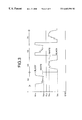
- FIG. 1 is a view showing schematic configuration of a liquid crystal display device
- FIG. 2 is an equivalent circuit diagram of a liquid crystal display device
- FIG. 3 is a timing chart showing an example of the image signal employed in the liquid crystal display device shown in FIG. 2;
- FIG. 4 is a schematic equivalent circuit diagram of a liquid crystal display device in which the present invention is applicable.
- FIG. 5 is a schematic timing chart showing an example of the image signal employed in the present invention.
- FIG. 6 is a schematic timing chart showing an example of the driving pulses of the present invention.
- FIG. 7 is a wave form chart showing an example of the signals employed in the present invention.
- FIG. 8 is a schematic equivalent circuit diagram of a liquid crystal display device in which the present invention is applicable.
- FIG. 9 is a schematic timing chart showing an example of the driving pulses employed in the present invention.
- FIG. 10 is a schematic timing chart showing an example of the image signal employed in the present invention.
- FIG. 11 is a schematic timing chart showing an example of the driving pulses employed in the present invention.
- a driving method for the liquid crystal display device provided with a plurality of pixels each of which is provided with a switching transistor receiving the supply of a signal inverted at a desired interval and an additional capacitance for retaining the signal voltage, wherein electrodes, one each, of said additional capacitances are commonly connected in each of desired blocks of said pixels, and the potential of said electrodes in a desired pixel block is varied after the supply of said signal to said pixel block.
- This method enables device drive with a low voltage and a high speed, thereby achieving reductions in size and cost of the liquid crystal display device.
- the common electrodes for liquid crystal driving and those of the additional capacitances are electrically separated, and the above-mentioned common electrodes of the additional capacitances are further separated for each vertical column of pixels, whereby the voltages applied to the common electrodes of said additional capacitances are rendered independently controllable.
- Such separation of the common electrodes reduces the capacitance of each group of common electrodes for example to about 9 pF, in case of about 500 pixels in the horizontal direction, so that the high-speed drive is significantly facilitated.
- transistors 42 , 42 ′, 46 , 46 ′ there are shown transistors 42 , 42 ′, 46 , 46 ′; common electrode lines 52 , 52 ′ for additional capacitances 9 ; and a common electrode line 54 to which connected are those of a common potential among the display electrodes of the liquid crystal pixels.
- V ab and V 3 indicate potentials applicable to the common electrode lines 52 , 52 ′.
- the common electrode lines 52 , 52 ′, . . . each commonly connected to the electrodes, one each, of the additional capacitances corresponding to the pixels of a horizontal row and thus constituting a block of pixels, are respectively connected to the transistors 42 , 42 ′; 46 , 46 ′; . . . controlled by the output of a vertical scanning circuit 10 .
- said transistors 42 , 42 ′, 46 , 46 ′, . . . are of p-MOS type, and each of address lines V 1 , V 2 , . . . receives, from the vertical scanning circuit 10 , an L-level pulse in a selected state or an H-level pulse in a non-selected state.
- the voltage V C1 of the common electrode line 52 common to the additional capacitances 9 , becomes equal to V ab or V 3 respectively when the address line V 1 is selected or not selected by the vertical scanning circuit 10 .
- the common electrodes 54 of the liquid crystal cells 5 receive a voltage V LC ′, while the voltage V ab assumes a potential V a or V b , and the voltage V 3 assumes a potential V a .
- the common electrode line 52 receives the voltage V a , and, in response to the horizontal scanning pulses H n , negative image signals within a range of V WH ′ to V DH ′ are supplied, in succession, to the liquid crystal cells 5 and the additional capacitances 9 , through the lines D 1 -D n and the switching transistors 7 .
- the pixels belonging to the address line V 1 retain the signal voltage same as at the signal entry, because of the non-conductive state of the transistors 7 , so that the voltage applied to the liquid crystal remains unchanged (cf. S 1 ′ in FIG. 7 ).
- the image signals of said range V DC ′ ⁇ V WL ′ are represented by voltages larger than the common electrode voltage V LC ′ for the liquid crystal 5 , approximately by a range of V WL ′ to V DL ′.
- the period of application of such unshifted improper voltage is about 50 ⁇ sec. at maximum, while the signal retaining period is about 17 to 33 msec., and the response of liquid crystal to the signal requires several to several ten milliseconds.
- the present embodiment shifts the voltage of the positive image signals by about V WL ′ ⁇ V DL ′, thereby correspondingly compress the entire signal voltage amplitude.
- the non-conductive portion of the signal resulting from the threshold voltage V th of the p-MOS transistor is compensated by the above-mentioned shift of the signal voltage.
- the voltages of the common electrode lines 52 , 52 ′, . . . of the additional capacitances 9 are controlled by transistors 48 , 48 ′, . . .
- a first plural wiring group comprising plural wirings 81 and 81 ′ connects commonly gate terminals of the transistors 7 on each of the rows.
- a second wiring group comprising plural wirings 82 and 82 ′ connects commonly source terminals of the transistors 7 on each of the columns.
- a common electrode 83 connects commonly the second capacitors, or liquid crystal, 5 connected to the drain terminals of the transistors 7 on the rows and columns.
- the voltages V C1 , V C2 , . . . to be applied to the common electrode lines 52 , 52 ′, . . . are controlled by the transistors 48 , 48 ′, . . . connected electrically thereto.
- the common electrode line for the pixels corresponding to the selected vertical address is given a voltage V ab , but, in the non-selected state, is maintained in a floating state with the voltage V ab .
- the liquid crystal 5 can thus be driven with the signals as shown in FIG. 5, by means of such voltage V ab and the on/off operations of the transistors.
- this embodiment can reduce the signal voltage amplitude as in the first embodiment, however, with a reduced number of transistors.
- This embodiment further reduces the signal voltage amplitude as will be explained in the following with reference to timing charts shown in FIGS. 10 and 11.
- the image signals of positive and negative polarities are so selected as to overlap with the common electrode voltage of the liquid crystal, thereby further reducing the entire signal voltage range by such overlapping portion.
- Such voltage shift after the voltage application at the entry of image signals into the pixels allows to apply a desired voltage to the liquid crystal and to further reduce the signal voltage range.
- the present invention is to reduce the amplitude of the input image signals, utilizing a variation in the voltage of the common electrodes of the additional capacitances between the write-in phase of the image signals and the signal retaining phase, and is not limited to the foregoing embodiments as long as the above-mentioned condition is met.
- it is applicable to the interlace drive with different combinations of vertical scanning operations, or to various image input methods such as dot-sequential input method or collective input method utilizing temporary retaining capacitances.
- the driving method of the present invention being capable of reducing the range of the input image signals through the control of the common electrode potential of the additional capacitances in the liquid crystal display device, allows to employ a lower voltage in the designing of liquid crystal panel and peripheral IC's, thereby achieving reductions in size, cost and power consumption of the display device.
Abstract
For enabling a liquid display drive with a low voltage and a high speed, each pixel is provided with a liquid crystal cell 5, a switching transistor 7 and an additional capacitance 9, and the additional capacitances are electrically commonly connected for a block of plural pixels. After the image signal is supplied to the pixels corresponding to the block, the potential of desired one of the common electrode lines 52, 52′, to which the additional capacitances 9 corresponding to the block are connected, is varied and retained at thus varied value.
Description
This application is a division of application Ser. No. 08/841,823, filed Apr. 28, 1997, which is a continuation of application Ser. No. 08/370,453, filed Jan. 9, 1995, abandoned, which is a continuation of application Ser. No. 08/233,404, filed Apr. 26, 1994, abandoned.
1. Field of the Invention
The present invention relates to a method for driving a liquid crystal display device, and more particularly to a method for driving a matrix liquid crystal display device having plural pixels arranged in a matrix.
2. Related Background Art
In recent years, the liquid crystal display devices are commercialized in various fields such as display for a word processor, a personal computer or the like, electronic view finder for a video camera, projection television or displays for an automobile. Also there is being required image display of a larger size, a higher resolution and a higher image quality.
FIG. 1 schematically shows the configuration of such liquid crystal display device, applied for a television receiver.
In FIG. 1 there are shown a vertical shift register 10; a horizontal shift register 20; switching transistors 22; a common signal line 24; a signal inverting circuit 30; a clock generator circuit 40; a liquid crystal display panel 100; address signal lines V1, V2, . . . , Vm−1, Vm; vertical data signal lines D1, D2, . . . , Dn; a signal S bearing image information; and an output signal S′ bearing image information, released from the signal inverting circuit 30.
The vertical data signal lines D1-Dn are connected, respectively through the horizontal transfer switches 22, to the signal line 24, and the gates of the horizontal transfer switches 22 receive signals from the horizontal shift register 20, in response to the signal from the clock generator circuit 40. The signal from the clock generator circuit 40 is also supplied to the vertical shift register 10, thus driving the address signal lines V1-Vm in succession in synchronization with the signal S. The signal from the clock generator circuit 40 is further supplied to the signal inverting circuit 30, thereby inverting the signal S in synchronization therewith. The clock generator circuit 40 is given an unrepresented synchronization signal, prepared from the image information bearing signal S, in order to achieve synchronization with the signal S.
In this manner the vertical shift register 10, the horizontal shift register 20 and the signal inverting circuit 30 effect the desired television scanning operation, by means of the pulses prepared by the clock generator 40.
In the liquid crystal panel 100, a row of pixels is selected by the address signal lines V1-Vm from the vertical shift register 10, and the vertical data signal lines D1-Dn are selected by the successive activations of the horizontal transfer switches 22 by driving pulses H1−Hm from the horizontal shift register 20, whereby image signals are supplied to the respective pixels.
As explained in the foregoing, the input terminals of the horizontal transfer switches 22 are connected, through the common signal line 24, to the signal inverting circuit 30, which is provided for converting the input image signal into an AC drive signal, in order to prevent deterioration in the characteristics of the liquid crystal. For AC driving of liquid crystal, there are already known various methods such as frame inversion, field inversion, 1H (horizontal scanning period) inversion and bit (every pixel) inversion.
FIG. 2 is an equivalent circuit of the liquid crystal panel 100 shown in FIG. 1. In FIG. 2, there are only shown four pixels driven with the data signal lines D1, D2 and the address signal lines V1, V2 within the liquid crystal panel 100.
Referring to FIG. 2, there are shown liquid crystal pixels 5; switching transistors 7 respectively attached to the pixels; common electrode lines 16; and additional capacitances 9. Electrodes of the liquid crystal pixel 5 and the additional capacitance 9 are electrically connected to the output side of the respective switching transistor 7, and the other electrodes are connected to the common electrode line 16. The input terminals of the switching transistors 7 are electrically connected, in groups of respective vertical columns of pixels, to the data signal lines D1, D2. Also the address signal lines V1, V2 are electrically connected, in groups of respective horizontal rows of pixels, to the gates of the switching transistors 7.
In FIG. 2, CLC and CS respectively indicate the equivalent capacitance of the liquid crystal pixel and the additional capacitance.
FIG. 3 is a timing chart showing an example of the output signal S′ from the signal inverting circuit 30. The input signal S bearing image information is converted into the output signal S′ by inversion by every 1H. In FIG. 3, VLC is the potential of the common electrode, VDL is the black level of the positive image signal, VWL is the white level thereof, VDH is the black level of the negative image signal, and VWH is the white level thereof.
As the signal inversion generates an image signal symmetrical to the common electrode potential VLC, the entire signal amplitude (VDL-VDH) is equal to twice of (VDL-VLC), so that it becomes about 10V if the potential difference between VDL and VLC is about 5 V.
In the circuit shown in FIG. 2, if the switching transistors 7 and the horizontal transfer switches 22 are composed of p-MOS transistors, each transistor becomes non-conductive in response to an input signal of a voltage lower than the threshold voltage Vth of said transistor. In most cases, for maintaining the non-conductive state in a range from the ground potential GND to VDL in consideration of the operating margin, the voltage of the image signal S′ becomes larger than the potential difference mentioned above. In the foregoing example, this signal voltage is usually taken as about 13 V or larger.
As the above-explained driving method involves a high driving voltage, a high voltage resistance is required in the driving devices for the liquid crystal display device, and a matching design is required for the wirings etc. This fact inevitably leads to a lowered production yield, a higher cost and a higher power consumption of the liquid crystal display device.
In order to overcome such drawbacks, there have been proposed methods as disclosed in the Japanese Patent Laid-open Application Nos. 54-98525 and 1-138590.
The method disclosed in the Japanese Patent Laid-open Application No. 54-98525 consists of inverting the common electrode potential VLC in synchronization with the inversion of the image signal S′, thereby selecting a same amplitude range for the positive and negative image signals and reducing the entire signal amplitude range to about ½.
However, such method may lead to the following difficulty.
Usually the liquid crystal capacitance CLC is in the order of several ten fF, while the additional capacitance CS is about 100 fF. If the total capacitance for a pixel is 100 fF, the total capacitance of the entire liquid crystal display device becomes about 10,000 pF when it is applied to a television display, as there are at least required 100,000 pixels.
Consequently, for driving such liquid crystal display device for example with a signal amplitude range of ca. 7 V, there is required a high-speed pulse drive of a load capacitance of 10,000 pF with a potential difference of ca. 7 V. Such requirement inevitably results in an increased magnitude and an elevated cost of the driving circuits.
Besides, the number of pixels of the liquid crystal display device is increasing, for achieving color display or a higher image quality. For this reason the capacitance of the device will correspondingly increase, for example to 30,000 pF for 300,000 pixels, or 50,000 pF for 500,000 pixels, so that cost reduction and compactization of the driving circuits will become more difficult to achieve.
On the other hand, the method disclosed in the Japanese Patent Laid-open Application No. 1-138590 consists of employing separate common electrodes for the liquid crystal and for the additional capacitance, and applying an inversion potential to the common electrode of the liquid crystal.
Also this method results in a similar difficulty, as a high-speed drive is required for a total liquid crystal capacitance of several thousand pF for example for 100,000 pixels.
Besides, in this case, the image signal voltage VLC′ applied to the liquid crystal for inverting the common electrode potential VLC for the liquid crystal of a capacitance smaller than the additional capacitance varies at maximum:
Consequently, though a proper voltage can be applied at the entry of the image signal to the liquid crystal, such voltage can no longer be applied during the voltage-maintaining period.
Such difficulty may be overcome by selecting the additional capacitance CS sufficiently smaller than the liquid crystal capacitance CLC, but, in such case, the total capacitance per pixel becomes too small for maintaining the signal voltage, so that satisfactory image display performance is difficult to obtain.
As explained in the foregoing, the conventional driving methods for the liquid crystal display device involves a very large signal voltage because of the threshold voltage Vth of the transistors present in the display device and also because of the image signal amplitude extending in the positive and negative polarities, thereby requiring designs with high voltage resistance in the signal processing IC, drive pulse generating IC, liquid crystal display panel, other peripheral circuits and wirings, thus leading to a larger dimension and an elevated cost of the liquid crystal display device.
In consideration of the foregoing, an object of the present invention is to provide a driving method for the liquid crystal display device, enabling drive with a lower voltage, thereby allowing to achieve compactization and cost reduction of the liquid crystal display device.
Another object of the present invention is to provide a driving method for the liquid crystal display device provided with a plurality of pixels each of which is provided with a switching transistor for receiving a signal inverted at a desired interval and an additional capacitance for maintaining the signal voltage, wherein one of the electrodes of said additional capacitance is commonly connected for a desired block of said pixels, and the potential of said electrode is varied after the supply of said signal.
Still another object of the present invention is to provide a driving method for the liquid crystal display device for effecting display by entry of a signal, inverted at a desired interval, through switching transistors to pixels respectively provided with additional capacitances, wherein electrodes, one each, of said additional capacitances and electrodes, one each, of the pixels are commonly but mutually separately connected electrically in each of desired blocks of the pixels, while the other electrodes of said additional capacitances and the other pixel electrodes are respectively connected to said switching transistors in each of said desired blocks, and, in at least one of said desired blocks, after said signal is supplied to the other electrodes of said additional capacitances and the other pixel electrodes through said switching transistors in a state in which a desired potential is supplied to the other electrodes of said additional capacitances, a potential different from said desired potential is supplied to the other electrodes of said additional capacitances.
FIG. 1 is a view showing schematic configuration of a liquid crystal display device;
FIG. 2 is an equivalent circuit diagram of a liquid crystal display device;
FIG. 3 is a timing chart showing an example of the image signal employed in the liquid crystal display device shown in FIG. 2;
FIG. 4 is a schematic equivalent circuit diagram of a liquid crystal display device in which the present invention is applicable;
FIG. 5 is a schematic timing chart showing an example of the image signal employed in the present invention;
FIG. 6 is a schematic timing chart showing an example of the driving pulses of the present invention;
FIG. 7 is a wave form chart showing an example of the signals employed in the present invention;
FIG. 8 is a schematic equivalent circuit diagram of a liquid crystal display device in which the present invention is applicable;
FIG. 9 is a schematic timing chart showing an example of the driving pulses employed in the present invention;
FIG. 10 is a schematic timing chart showing an example of the image signal employed in the present invention; and
FIG. 11 is a schematic timing chart showing an example of the driving pulses employed in the present invention.
The aforementioned objects can be attained by a driving method for the liquid crystal display device provided with a plurality of pixels each of which is provided with a switching transistor receiving the supply of a signal inverted at a desired interval and an additional capacitance for retaining the signal voltage, wherein electrodes, one each, of said additional capacitances are commonly connected in each of desired blocks of said pixels, and the potential of said electrodes in a desired pixel block is varied after the supply of said signal to said pixel block.
This method enables device drive with a low voltage and a high speed, thereby achieving reductions in size and cost of the liquid crystal display device.
In the following the driving method of the present invention will be clarified in detail, with reference to the attached drawings.
In this embodiment, the common electrodes for liquid crystal driving and those of the additional capacitances are electrically separated, and the above-mentioned common electrodes of the additional capacitances are further separated for each vertical column of pixels, whereby the voltages applied to the common electrodes of said additional capacitances are rendered independently controllable. Such separation of the common electrodes reduces the capacitance of each group of common electrodes for example to about 9 pF, in case of about 500 pixels in the horizontal direction, so that the high-speed drive is significantly facilitated.
In the following a more detailed explanation will be given with reference to a schematic equivalent circuit diagram shown in FIG. 4, schematic timing charts shown in FIGS. 5 and 6 and a wave form chart shown in FIG. 7.
In FIG. 4 there are shown transistors 42, 42′, 46, 46′; common electrode lines 52, 52′ for additional capacitances 9; and a common electrode line 54 to which connected are those of a common potential among the display electrodes of the liquid crystal pixels. Vab and V3 indicate potentials applicable to the common electrode lines 52, 52′.
The common electrode lines 52, 52′, . . . , each commonly connected to the electrodes, one each, of the additional capacitances corresponding to the pixels of a horizontal row and thus constituting a block of pixels, are respectively connected to the transistors 42, 42′; 46, 46′; . . . controlled by the output of a vertical scanning circuit 10.
In this embodiment, said transistors 42, 42′, 46, 46′, . . . are of p-MOS type, and each of address lines V1, V2, . . . receives, from the vertical scanning circuit 10, an L-level pulse in a selected state or an H-level pulse in a non-selected state. Thus the voltage VC1 of the common electrode line 52, common to the additional capacitances 9, becomes equal to Vab or V3 respectively when the address line V1 is selected or not selected by the vertical scanning circuit 10.
In the present embodiment, as shown in FIGS. 5 and 6, the common electrodes 54 of the liquid crystal cells 5 receive a voltage VLC′, while the voltage Vab assumes a potential Va or Vb, and the voltage V3 assumes a potential Va.
Consequently, when the address line V1 is selected, the common electrode line 52 receives the voltage Va, and, in response to the horizontal scanning pulses Hn, negative image signals within a range of VWH′ to VDH′ are supplied, in succession, to the liquid crystal cells 5 and the additional capacitances 9, through the lines D1-Dn and the switching transistors 7.
Then, when the address line V2 is selected (address line V1 being shifted to the non-selected state), the address line V1 assumes the H-level potential, and the voltage VC1 of the common electrode line 52 is shifted from Vab (=Va) to V3. However, the voltage VC1 in fact does not vary, because Vab=V3=V1.
Consequently, the pixels belonging to the address line V1 retain the signal voltage same as at the signal entry, because of the non-conductive state of the transistors 7, so that the voltage applied to the liquid crystal remains unchanged (cf. S1′ in FIG. 7).
On the other hand, by the selection of the address line V2, the voltage VC2 of the common electrode line 52′ assumes a value Vab=Vb, and, in response to the horizontal scanning pulses Hn, the positive image signals within a range of VDC′ to VWL′ are similarly supplied to the liquid crystal cells.
The image signals of said range VDC′−VWL′ are represented by voltages larger than the common electrode voltage VLC′ for the liquid crystal 5, approximately by a range of VWL′ to VDL′. When the next vertical address line is selected after the scanning of the pixels corresponding to the address line V2, the vertical address line V2 assumes the H-level state, whereby the voltage VC2 assumes the potential V3=Va.
In this manner the voltage VC2 becomes Vb at the application of the image signal, and is shifted to Va while the image signal is retained. This potential shift of −(Vb-Va) causes the liquid crystal 5 to receive the image signal of a proper voltage (cf. S2″ in FIG. 7).
The application of unshifted “improper” voltage at the image signal application does not detrimentally affect the image display performance, because the period of such application is extremely shorter than the signal retaining period and also because the response of the liquid crystal to the signal is slower.
More specifically, the period of application of such unshifted improper voltage is about 50 μsec. at maximum, while the signal retaining period is about 17 to 33 msec., and the response of liquid crystal to the signal requires several to several ten milliseconds.
As explained in the foregoing, the present embodiment shifts the voltage of the positive image signals by about VWL′−VDL′, thereby correspondingly compress the entire signal voltage amplitude.
Stated differently, the non-conductive portion of the signal resulting from the threshold voltage Vth of the p-MOS transistor is compensated by the above-mentioned shift of the signal voltage.
In this embodiment, as shown in a schematic equivalent circuit diagram in FIG. 8, the voltages of the common electrode lines 52, 52′, . . . of the additional capacitances 9 are controlled by transistors 48, 48′, . . .
In FIG. 8, a first plural wiring group comprising plural wirings 81 and 81′ connects commonly gate terminals of the transistors 7 on each of the rows. A second wiring group comprising plural wirings 82 and 82′ connects commonly source terminals of the transistors 7 on each of the columns. A common electrode 83 connects commonly the second capacitors, or liquid crystal, 5 connected to the drain terminals of the transistors 7 on the rows and columns.
This embodiment will be explained further in the following, with reference also to a schematic timing chart in FIG. 9.
In this embodiment, the voltages VC1, VC2, . . . to be applied to the common electrode lines 52, 52′, . . . are controlled by the transistors 48, 48′, . . . connected electrically thereto. In this embodiment, the common electrode line for the pixels corresponding to the selected vertical address is given a voltage Vab , but, in the non-selected state, is maintained in a floating state with the voltage Vab .
Referring to FIG. 9, when the vertical address line V1 is selected, the transistor 48 is turned on to apply Vab (=Va) as the voltage VC1 of the common electrode line 52. Then, when the vertical address line V2 is selected and the vertical address line V1 is shifted to the non-selected state, the transistor 48 is turned off whereby the common electrode line 52 is maintained in the floating state with a voltage Va while the transistor 48′ is turned on to apply Vab (=Vb) to the common electrode line 52′.
The liquid crystal 5 can thus be driven with the signals as shown in FIG. 5, by means of such voltage Vab and the on/off operations of the transistors.
As explained in the foregoing, this embodiment can reduce the signal voltage amplitude as in the first embodiment, however, with a reduced number of transistors.
This embodiment further reduces the signal voltage amplitude as will be explained in the following with reference to timing charts shown in FIGS. 10 and 11.
In this embodiment, the image signals of positive and negative polarities are so selected as to overlap with the common electrode voltage of the liquid crystal, thereby further reducing the entire signal voltage range by such overlapping portion.
More specifically, when the vertical address line V1 is selected, the negative image signals are applied with VC1=Va, and the voltage is shifted to VC1=Vb after said application, whereby a proper voltage is applied during the signal retaining phase. Similarly, when the vertical address line V2 is selected, the positive image signals are applied with VC2=Vb, and the voltage is shifted to VC2=Va after said application, whereby a proper voltage is applied during the signal retaining phase.
Such voltage shift after the voltage application at the entry of image signals into the pixels allows to apply a desired voltage to the liquid crystal and to further reduce the signal voltage range.
In summary, the present invention is to reduce the amplitude of the input image signals, utilizing a variation in the voltage of the common electrodes of the additional capacitances between the write-in phase of the image signals and the signal retaining phase, and is not limited to the foregoing embodiments as long as the above-mentioned condition is met. For example it is applicable to the interlace drive with different combinations of vertical scanning operations, or to various image input methods such as dot-sequential input method or collective input method utilizing temporary retaining capacitances.
As explained in the foregoing, the driving method of the present invention, being capable of reducing the range of the input image signals through the control of the common electrode potential of the additional capacitances in the liquid crystal display device, allows to employ a lower voltage in the designing of liquid crystal panel and peripheral IC's, thereby achieving reductions in size, cost and power consumption of the display device.
Claims (8)
1. A liquid crystal display device comprising:
a matrix wiring of row wirings and column wirings;
a liquid crystal pixel element at each cross point of the matrix wiring, the pixel element comprising a liquid crystal cell, switching transistor, and capacitor, a first terminal of the cell and a first terminal of the capacitor being connected at a joint point, which is in turn connected to one of the column wirings through the switching transistor, and a second terminal of the cell being connected to a reference potential;
a video signal drive circuit for applying a video signal to each of the column wirings through a transfer switch;
a selection signal drive circuit for applying a selection signal sequentially to each of the row wirings, the selection signal drive circuit, in cooperation with the video signal drive circuit, applying the video signal to the joint point of each pixel element through the transfer switch and the switching transistor to charge the capacitor of each pixel element by the video signal, wherein the video signal is a modified video signal derived from a normal video signal comprising an inverted video signal and a non-inverted video signal, said deriving occuring by shifting the DC level, or levels, of the inverted video signal and/or the non-inverted video signal so that the amplitude width of the modified video signal is narrower than that of the normal video signal; and
a control circuit for applying a first potential to a second terminal of the capacitor at each pixel element in a first group for a first period, while the video signal is being applied to the joint point associated with each pixel in said first group, and for applying a second potential to the second terminal of the capacitor at each pixel element in a second group for at least part of a second period, while the video signal is not being applied to the joint point associated with each pixel element in said second group,
wherein the first potential and the second potential are selected so that a charge built up in the capacitor at each pixel element in said second group provides a potential at the associated joint point which corresponds to the normal video signal by compensating for a DC shift in the second period.
2. The liquid crystal device according to claim 1 , wherein in the modified video signal, a DC level in either one of the inverted video signal or non-inverted video signal is shifted, and wherein, for the capacitor associated with the cell to which the video signal without DC level shift is applied, the first potential is equal to the second potential.
3. The liquid crystal device according to claim 1 , wherein the inverted video signal and the non-inverted video signal have a period corresponding to one horizontal scanning period, respectively.
4. The liquid crystal device according to claim 3 , wherein the first period corresponds to the horizontal scanning period.
5. The liquid crystal device according to claim 1 , wherein the first period corresponds to a period while the transfer switch is being turned on.
6. The liquid crystal device according to claim 1 , wherein the inverted video signal is inverted with respect to the reference potential for the normal video signal.
7. The liquid crystal device according to claim 1 , wherein the control circuit applies the first potential to a common line which is connected to the second terminal of the capacitor at each of pixel elements associated with the row wiring to which the selection signal is being applied, and applies the second potential to common lines which are connected to the second terminal of the capacitor at each of pixel elements associated with the row wirings to which the selection signal is not being applied.
8. A liquid crystal display device comprising:
a matrix wiring of row wirings and column wirings;
a liquid crystal pixel element at each cross point of the matrix wiring, the pixel element comprising a liquid crystal cell, switching transistor, and capacitor, a first terminal of the cell and a first terminal of the capacitor being connected at a joint point, which is in turn connected to one of the column wirings through the switching transistor, and a second terminal of the cell being connected to a reference potential;
a video signal drive circuit for applying a video signal to each of the column wirings through a transfer switch;
a selection signal drive circuit for applying a selection signal sequentially to each of the row wirings, the selection signal drive circuit, in cooperation with the video signal drive circuit, applying the video signal to the joint point of each pixel element through the transfer switch and the switching transistor to charge the capacitor of each pixel element by the video signal, wherein the video signal is a modified video signal derived from a normal video signal comprising an inverted video signal and a non-inverted video signal, said deriving occurring by shifting the DC level, or levels, of the inverted video signal and/or the non-inverted video signal so that the amplitude width of the modified video signal is narrower than that of the normal video signal; and
a control circuit for applying (1) a first potential to a first common line connected to a second terminal of the capacitor at each pixel element in a first group for a first period, while the switching transistor is in an ON state and the video signal is being applied to the joint point associated with each pixel element in said first group, (2) a second potential to a second common line connected to a second terminal of the capacitor at each pixel element in a second group for a second period, while the switching transistor is in an ON state and the video signal is being applied to the joint point associated with each pixel element in said first group, and (3) the first potential to the second common line connected to the second terminal of the capacitor at each pixel element in said second group for a third period, while the switching transistor is in an ON state and the video signal is not being applied to the joint point associated with each pixel element in said second group,
wherein the first potential and the second potential are selected so that a charge built up in the capacitor at each pixel element in said second group provides a potential at the associated joint point which corresponds to the normal video signal by compensating for a DC shift in the third period.
Priority Applications (1)
| Application Number | Priority Date | Filing Date | Title |
|---|---|---|---|
| US09/459,480 US6683591B2 (en) | 1993-04-28 | 1999-12-13 | Method for driving liquid crystal display device |
Applications Claiming Priority (6)
| Application Number | Priority Date | Filing Date | Title |
|---|---|---|---|
| JP5-102731 | 1993-04-28 | ||
| JP10273193A JPH06313876A (en) | 1993-04-28 | 1993-04-28 | Drive method for liquid crystal display device |
| US23340494A | 1994-04-26 | 1994-04-26 | |
| US37045395A | 1995-01-09 | 1995-01-09 | |
| US08/841,823 US6031514A (en) | 1993-04-28 | 1997-04-28 | Method for driving liquid crystal display device |
| US09/459,480 US6683591B2 (en) | 1993-04-28 | 1999-12-13 | Method for driving liquid crystal display device |
Related Parent Applications (1)
| Application Number | Title | Priority Date | Filing Date |
|---|---|---|---|
| US08/841,823 Division US6031514A (en) | 1993-04-28 | 1997-04-28 | Method for driving liquid crystal display device |
Publications (2)
| Publication Number | Publication Date |
|---|---|
| US20020105489A1 US20020105489A1 (en) | 2002-08-08 |
| US6683591B2 true US6683591B2 (en) | 2004-01-27 |
Family
ID=14335400
Family Applications (2)
| Application Number | Title | Priority Date | Filing Date |
|---|---|---|---|
| US08/841,823 Expired - Fee Related US6031514A (en) | 1993-04-28 | 1997-04-28 | Method for driving liquid crystal display device |
| US09/459,480 Expired - Fee Related US6683591B2 (en) | 1993-04-28 | 1999-12-13 | Method for driving liquid crystal display device |
Family Applications Before (1)
| Application Number | Title | Priority Date | Filing Date |
|---|---|---|---|
| US08/841,823 Expired - Fee Related US6031514A (en) | 1993-04-28 | 1997-04-28 | Method for driving liquid crystal display device |
Country Status (3)
| Country | Link |
|---|---|
| US (2) | US6031514A (en) |
| EP (1) | EP0623911A1 (en) |
| JP (1) | JPH06313876A (en) |
Cited By (11)
| Publication number | Priority date | Publication date | Assignee | Title |
|---|---|---|---|---|
| US20030234902A1 (en) * | 2002-05-29 | 2003-12-25 | Kabushiki Kaisha Toshiba | Display device |
| US20040095298A1 (en) * | 2002-08-30 | 2004-05-20 | Seiko Epson Corporation | Electronic circuit, method of driving electronic circuit, electro-optical device, method of driving electro-optical device, and electronic apparatus |
| US20060270083A1 (en) * | 2005-05-26 | 2006-11-30 | Seiko Epson Corporation | Electro-optical device and electronic apparatus having the same |
| US20070152936A1 (en) * | 2005-12-30 | 2007-07-05 | Shin Hyung B | Liquid crystal display device and driving method thereof |
| US20070170531A1 (en) * | 2006-01-20 | 2007-07-26 | Aaron Partridge | Wafer encapsulated microelectromechanical structure and method of manufacturing same |
| US7463403B1 (en) * | 2005-04-22 | 2008-12-09 | Silicon Light Machines Corporation | High impedance drive circuit for a micro-electromechanical system device |
| US20090117859A1 (en) * | 2006-04-07 | 2009-05-07 | Belair Networks Inc. | System and method for frequency offsetting of information communicated in mimo based wireless networks |
| US20090180466A1 (en) * | 2006-04-07 | 2009-07-16 | Belair Networks | System and method for frequency offsetting of information communicated in mimo-based wireless networks |
| US20110124308A1 (en) * | 2006-04-07 | 2011-05-26 | Belair Networks Inc. | System and method for zero intermediate frequency filtering of information communicated in wireless networks |
| US10847116B2 (en) | 2009-11-30 | 2020-11-24 | Semiconductor Energy Laboratory Co., Ltd. | Reducing pixel refresh rate for still images using oxide transistors |
| US11062667B2 (en) | 2016-11-25 | 2021-07-13 | Semiconductor Energy Laboratory Co., Ltd. | Display device and operating method thereof |
Families Citing this family (22)
| Publication number | Priority date | Publication date | Assignee | Title |
|---|---|---|---|---|
| US4867980A (en) * | 1986-10-10 | 1989-09-19 | Coopers Animal Health Australia Limited | Heavy density depot |
| EP0686958B1 (en) | 1994-06-06 | 2003-10-29 | Canon Kabushiki Kaisha | DC compensation for interlaced display |
| US6911962B1 (en) | 1996-03-26 | 2005-06-28 | Semiconductor Energy Laboratory Co., Ltd. | Driving method of active matrix display device |
| US6670938B1 (en) | 1999-02-16 | 2003-12-30 | Canon Kabushiki Kaisha | Electronic circuit and liquid crystal display apparatus including same |
| US6868154B1 (en) * | 1999-08-02 | 2005-03-15 | Robert O. Stuart | System and method for providing a service to a customer via a communication link |
| KR100770543B1 (en) * | 2001-03-20 | 2007-10-25 | 엘지.필립스 엘시디 주식회사 | Liquid Crystal Display Device And Driving Method Thereof |
| JP2005173244A (en) * | 2003-12-11 | 2005-06-30 | Toshiba Matsushita Display Technology Co Ltd | Liquid crystal display device, and display method of liquid crystal display panel |
| US7652649B2 (en) * | 2005-06-15 | 2010-01-26 | Au Optronics Corporation | LCD device with improved optical performance |
| JP4797823B2 (en) * | 2005-10-03 | 2011-10-19 | セイコーエプソン株式会社 | Electro-optical device, driving method of electro-optical device, and electronic apparatus |
| TWI449009B (en) * | 2005-12-02 | 2014-08-11 | Semiconductor Energy Lab | Display device and electronic device using the same |
| TW200746022A (en) * | 2006-04-19 | 2007-12-16 | Ignis Innovation Inc | Stable driving scheme for active matrix displays |
| KR101352936B1 (en) * | 2006-11-29 | 2014-01-16 | 엘지디스플레이 주식회사 | Liquid crystal display device |
| TWI348065B (en) * | 2007-01-10 | 2011-09-01 | Au Optronics Corp | Liquid crystal display |
| CN100492115C (en) * | 2007-07-12 | 2009-05-27 | 昆山龙腾光电有限公司 | Regulating device and method for reducing liquid crystal display panel scintillation and liquid crystal display panel |
| US7884891B2 (en) * | 2008-01-21 | 2011-02-08 | Beijing Boe Optoelectronics Technology Co., Ltd. | Thin film transistor liquid crystal display |
| CN101770750B (en) * | 2008-12-26 | 2012-01-25 | 北京京东方光电科技有限公司 | Liquid crystal display and control method thereof |
| TWI395033B (en) * | 2009-03-17 | 2013-05-01 | Wintek Corp | Lcd panel |
| TWI384307B (en) * | 2009-04-13 | 2013-02-01 | Au Optronics Corp | Liquid crystal display |
| KR101900662B1 (en) * | 2009-12-18 | 2018-11-08 | 가부시키가이샤 한도오따이 에네루기 켄큐쇼 | Liquid crystal display device and driving method thereof |
| US8633889B2 (en) | 2010-04-15 | 2014-01-21 | Semiconductor Energy Laboratory Co., Ltd. | Display device, driving method thereof, and electronic appliance |
| TWI534773B (en) | 2010-04-23 | 2016-05-21 | 半導體能源研究所股份有限公司 | Method for driving display device |
| TWI670552B (en) * | 2018-05-25 | 2019-09-01 | 友達光電股份有限公司 | Lcd and control method thereof |
Citations (18)
| Publication number | Priority date | Publication date | Assignee | Title |
|---|---|---|---|---|
| JPS5498525A (en) | 1978-01-20 | 1979-08-03 | Matsushita Electric Ind Co Ltd | Driving circuit for liquid crystal display unit |
| US4206386A (en) * | 1977-04-18 | 1980-06-03 | Matsushita Electric Industrial Co., Ltd. | Gas discharge display device |
| US4386352A (en) | 1978-02-08 | 1983-05-31 | Sharp Kabushiki Kaisha | Matrix type liquid crystal display |
| US4393380A (en) | 1979-05-28 | 1983-07-12 | Kabushiki Kaisha Suwa Seikosha | Liquid crystal display systems |
| US4429305A (en) * | 1979-05-30 | 1984-01-31 | Kabushiki, Kaisha Suwa Seikosha | Liquid crystal display system |
| US4789223A (en) * | 1985-03-28 | 1988-12-06 | Kabushiki Kaisha Toshiba | Matrix-addressed liquid crystal display device with compensation for potential shift of pixel electrodes |
| US4795239A (en) * | 1985-08-29 | 1989-01-03 | Canon Kabushiki Kaisha | Method of driving a display panel |
| JPH01138590A (en) | 1988-08-25 | 1989-05-31 | Seiko Epson Corp | Liquid crystal display device |
| US4999618A (en) * | 1987-06-17 | 1991-03-12 | Sharp Kabushiki Kaisha | Driving method of thin film EL display unit and driving circuit thereof |
| US5105288A (en) * | 1989-10-18 | 1992-04-14 | Matsushita Electronics Corporation | Liquid crystal display apparatus with the application of black level signal for suppressing light leakage |
| US5151805A (en) | 1989-11-28 | 1992-09-29 | Matsushita Electric Industrial Co., Ltd. | Capacitively coupled driving method for TFT-LCD to compensate for switching distortion and to reduce driving power |
| US5477243A (en) * | 1990-02-26 | 1995-12-19 | Canon Kabushiki Kaisha | Method of operating and an apparatus using an ink jet head having serially connected energy generating means |
| US5528396A (en) * | 1987-06-10 | 1996-06-18 | Hitachi, Ltd. | TFT active matrix liquid crystal display devices with a holding capacitance between the pixel electrode and a scanning signal line |
| US5682177A (en) * | 1991-07-08 | 1997-10-28 | Asahi Glass Company Ltd. | Driving method of driving a liquid crystal display element |
| US5686932A (en) * | 1991-10-04 | 1997-11-11 | Kabushiki Kaisha Toshiba | Compensative driving method type liquid crystal display device |
| US5706123A (en) * | 1996-09-27 | 1998-01-06 | Texas Instruments Incorporated | Switched control signals for digital micro-mirror device with split reset |
| US5784073A (en) * | 1991-06-14 | 1998-07-21 | Semiconductor Energy Laboratory Co., Ltd. | Electro-optical device and method of driving the same |
| US5828354A (en) * | 1990-07-13 | 1998-10-27 | Citizen Watch Co., Ltd. | Electrooptical display device |
Family Cites Families (1)
| Publication number | Priority date | Publication date | Assignee | Title |
|---|---|---|---|---|
| JP2714993B2 (en) * | 1989-12-15 | 1998-02-16 | セイコーエプソン株式会社 | Liquid crystal display |
-
1993
- 1993-04-28 JP JP10273193A patent/JPH06313876A/en active Pending
-
1994
- 1994-04-27 EP EP94106559A patent/EP0623911A1/en not_active Withdrawn
-
1997
- 1997-04-28 US US08/841,823 patent/US6031514A/en not_active Expired - Fee Related
-
1999
- 1999-12-13 US US09/459,480 patent/US6683591B2/en not_active Expired - Fee Related
Patent Citations (18)
| Publication number | Priority date | Publication date | Assignee | Title |
|---|---|---|---|---|
| US4206386A (en) * | 1977-04-18 | 1980-06-03 | Matsushita Electric Industrial Co., Ltd. | Gas discharge display device |
| JPS5498525A (en) | 1978-01-20 | 1979-08-03 | Matsushita Electric Ind Co Ltd | Driving circuit for liquid crystal display unit |
| US4386352A (en) | 1978-02-08 | 1983-05-31 | Sharp Kabushiki Kaisha | Matrix type liquid crystal display |
| US4393380A (en) | 1979-05-28 | 1983-07-12 | Kabushiki Kaisha Suwa Seikosha | Liquid crystal display systems |
| US4429305A (en) * | 1979-05-30 | 1984-01-31 | Kabushiki, Kaisha Suwa Seikosha | Liquid crystal display system |
| US4789223A (en) * | 1985-03-28 | 1988-12-06 | Kabushiki Kaisha Toshiba | Matrix-addressed liquid crystal display device with compensation for potential shift of pixel electrodes |
| US4795239A (en) * | 1985-08-29 | 1989-01-03 | Canon Kabushiki Kaisha | Method of driving a display panel |
| US5528396A (en) * | 1987-06-10 | 1996-06-18 | Hitachi, Ltd. | TFT active matrix liquid crystal display devices with a holding capacitance between the pixel electrode and a scanning signal line |
| US4999618A (en) * | 1987-06-17 | 1991-03-12 | Sharp Kabushiki Kaisha | Driving method of thin film EL display unit and driving circuit thereof |
| JPH01138590A (en) | 1988-08-25 | 1989-05-31 | Seiko Epson Corp | Liquid crystal display device |
| US5105288A (en) * | 1989-10-18 | 1992-04-14 | Matsushita Electronics Corporation | Liquid crystal display apparatus with the application of black level signal for suppressing light leakage |
| US5151805A (en) | 1989-11-28 | 1992-09-29 | Matsushita Electric Industrial Co., Ltd. | Capacitively coupled driving method for TFT-LCD to compensate for switching distortion and to reduce driving power |
| US5477243A (en) * | 1990-02-26 | 1995-12-19 | Canon Kabushiki Kaisha | Method of operating and an apparatus using an ink jet head having serially connected energy generating means |
| US5828354A (en) * | 1990-07-13 | 1998-10-27 | Citizen Watch Co., Ltd. | Electrooptical display device |
| US5784073A (en) * | 1991-06-14 | 1998-07-21 | Semiconductor Energy Laboratory Co., Ltd. | Electro-optical device and method of driving the same |
| US5682177A (en) * | 1991-07-08 | 1997-10-28 | Asahi Glass Company Ltd. | Driving method of driving a liquid crystal display element |
| US5686932A (en) * | 1991-10-04 | 1997-11-11 | Kabushiki Kaisha Toshiba | Compensative driving method type liquid crystal display device |
| US5706123A (en) * | 1996-09-27 | 1998-01-06 | Texas Instruments Incorporated | Switched control signals for digital micro-mirror device with split reset |
Cited By (26)
| Publication number | Priority date | Publication date | Assignee | Title |
|---|---|---|---|---|
| US6839119B2 (en) * | 2002-05-29 | 2005-01-04 | Kabushiki Kaisha Toshiba | Display device |
| US20030234902A1 (en) * | 2002-05-29 | 2003-12-25 | Kabushiki Kaisha Toshiba | Display device |
| US20040095298A1 (en) * | 2002-08-30 | 2004-05-20 | Seiko Epson Corporation | Electronic circuit, method of driving electronic circuit, electro-optical device, method of driving electro-optical device, and electronic apparatus |
| US20060132399A1 (en) * | 2002-08-30 | 2006-06-22 | Seiko Epson Corporation | Electronic circuit, method of driving electronic circuit, electro-optical device, method of driving electro-optical device, and electronic apparatus |
| US7158105B2 (en) * | 2002-08-30 | 2007-01-02 | Seiko Epson Corporation | Electronic circuit, method of driving electronic circuit, electro-optical device, method of driving electro-optical device, and electronic apparatus |
| US7880690B2 (en) | 2002-08-30 | 2011-02-01 | Seiko Epson Corporation | Electronic circuit, method of driving electronic circuit, electro-optical device, method of driving electro-optical device, and electronic apparatus |
| US7463403B1 (en) * | 2005-04-22 | 2008-12-09 | Silicon Light Machines Corporation | High impedance drive circuit for a micro-electromechanical system device |
| US7742017B2 (en) * | 2005-05-26 | 2010-06-22 | Seiko Epson Corporation | Electro-optical device and electronic apparatus having the same |
| US20060270083A1 (en) * | 2005-05-26 | 2006-11-30 | Seiko Epson Corporation | Electro-optical device and electronic apparatus having the same |
| US20070152936A1 (en) * | 2005-12-30 | 2007-07-05 | Shin Hyung B | Liquid crystal display device and driving method thereof |
| US8144089B2 (en) * | 2005-12-30 | 2012-03-27 | Lg Display Co., Ltd. | Liquid crystal display device and driving method thereof |
| US20070170531A1 (en) * | 2006-01-20 | 2007-07-26 | Aaron Partridge | Wafer encapsulated microelectromechanical structure and method of manufacturing same |
| US8447232B2 (en) | 2006-04-07 | 2013-05-21 | Belair Networks Inc. | System and method for frequency offsetting of information communicated in MIMO-based wireless networks |
| US8583066B2 (en) | 2006-04-07 | 2013-11-12 | Belair Networks Inc. | System and method for frequency offsetting of information communicated in MIMO-based wireless networks |
| US20090117859A1 (en) * | 2006-04-07 | 2009-05-07 | Belair Networks Inc. | System and method for frequency offsetting of information communicated in mimo based wireless networks |
| US8254865B2 (en) | 2006-04-07 | 2012-08-28 | Belair Networks | System and method for frequency offsetting of information communicated in MIMO-based wireless networks |
| US8280337B2 (en) | 2006-04-07 | 2012-10-02 | Belair Networks Inc. | System and method for zero intermediate frequency filtering of information communicated in wireless networks |
| US8433254B2 (en) | 2006-04-07 | 2013-04-30 | Belair Networks Inc. | System and method for frequency offsetting of information communicated in MIMO-based wireless networks |
| US20090180466A1 (en) * | 2006-04-07 | 2009-07-16 | Belair Networks | System and method for frequency offsetting of information communicated in mimo-based wireless networks |
| US20110124308A1 (en) * | 2006-04-07 | 2011-05-26 | Belair Networks Inc. | System and method for zero intermediate frequency filtering of information communicated in wireless networks |
| US10847116B2 (en) | 2009-11-30 | 2020-11-24 | Semiconductor Energy Laboratory Co., Ltd. | Reducing pixel refresh rate for still images using oxide transistors |
| US11282477B2 (en) | 2009-11-30 | 2022-03-22 | Semiconductor Energy Laboratory Co., Ltd. | Liquid crystal display device, method for driving the same, and electronic device including the same |
| US11636825B2 (en) | 2009-11-30 | 2023-04-25 | Semiconductor Energy Laboratory Co., Ltd. | Liquid crystal display device, method for driving the same, and electronic device including the same |
| US11062667B2 (en) | 2016-11-25 | 2021-07-13 | Semiconductor Energy Laboratory Co., Ltd. | Display device and operating method thereof |
| US11361726B2 (en) | 2016-11-25 | 2022-06-14 | Semiconductor Energy Laboratory Co., Ltd. | Display device and operating method thereof |
| US11715438B2 (en) | 2016-11-25 | 2023-08-01 | Semiconductor Energy Laboratory Co., Ltd. | Display device and operating method thereof |
Also Published As
| Publication number | Publication date |
|---|---|
| JPH06313876A (en) | 1994-11-08 |
| EP0623911A1 (en) | 1994-11-09 |
| US20020105489A1 (en) | 2002-08-08 |
| US6031514A (en) | 2000-02-29 |
Similar Documents
| Publication | Publication Date | Title |
|---|---|---|
| US6683591B2 (en) | Method for driving liquid crystal display device | |
| US5510805A (en) | Scanning circuit | |
| US6075505A (en) | Active matrix liquid crystal display | |
| US5598180A (en) | Active matrix type display apparatus | |
| EP1202245B1 (en) | Dot-inversion data driver for liquid-crystal display device with reduced power consumption | |
| US6219022B1 (en) | Active matrix display and image forming system | |
| US7812807B2 (en) | Display device and driving device | |
| US5648790A (en) | Display scanning circuit | |
| KR100413937B1 (en) | Matrix display device | |
| KR100272873B1 (en) | Active-matrix display system with less signal line drive circuits | |
| KR100561946B1 (en) | Liquid crystal display device and driving method of the same | |
| JPH01202793A (en) | Matrix display device | |
| KR100549983B1 (en) | Liquid crystal display device and driving method of the same | |
| US5777591A (en) | Matrix display apparatus employing dual switching means and data signal line driving means | |
| JPH1185115A (en) | Liquid crystal and its driving method, projection type display device using it and electronic equipment | |
| US20020196247A1 (en) | Display device | |
| JPH08273387A (en) | Thin film integrated circuit | |
| KR100648141B1 (en) | Display device and drive method thereof | |
| US20030058207A1 (en) | Image display device and display driving method | |
| KR20040025599A (en) | Memory Circuit, Display Circuit, and Display Device | |
| JP2675060B2 (en) | Active matrix display device, scanning circuit thereof, and driving circuit of scanning circuit | |
| KR100761612B1 (en) | Electro-optical device and electronic apparatus | |
| JP3131411B2 (en) | Liquid crystal display device | |
| US20020186190A1 (en) | Device and method for addressing LCD pixels | |
| JP2004533018A5 (en) |
Legal Events
| Date | Code | Title | Description |
|---|---|---|---|
| FEPP | Fee payment procedure |
Free format text: PAYOR NUMBER ASSIGNED (ORIGINAL EVENT CODE: ASPN); ENTITY STATUS OF PATENT OWNER: LARGE ENTITY |
|
| CC | Certificate of correction | ||
| REMI | Maintenance fee reminder mailed | ||
| LAPS | Lapse for failure to pay maintenance fees | ||
| STCH | Information on status: patent discontinuation |
Free format text: PATENT EXPIRED DUE TO NONPAYMENT OF MAINTENANCE FEES UNDER 37 CFR 1.362 |
|
| FP | Lapsed due to failure to pay maintenance fee |
Effective date: 20080127 |