US6682628B2 - Methods and apparatuses for monitoring and controlling mechanical or chemical-mechanical planarization of microelectronic substrate assemblies - Google Patents
Methods and apparatuses for monitoring and controlling mechanical or chemical-mechanical planarization of microelectronic substrate assemblies Download PDFInfo
- Publication number
- US6682628B2 US6682628B2 US10/139,299 US13929902A US6682628B2 US 6682628 B2 US6682628 B2 US 6682628B2 US 13929902 A US13929902 A US 13929902A US 6682628 B2 US6682628 B2 US 6682628B2
- Authority
- US
- United States
- Prior art keywords
- substrate assembly
- planarizing
- substrate
- platen
- force detector
- Prior art date
- Legal status (The legal status is an assumption and is not a legal conclusion. Google has not performed a legal analysis and makes no representation as to the accuracy of the status listed.)
- Expired - Lifetime, expires
Links
Images


Classifications
-
- B—PERFORMING OPERATIONS; TRANSPORTING
- B24—GRINDING; POLISHING
- B24B—MACHINES, DEVICES, OR PROCESSES FOR GRINDING OR POLISHING; DRESSING OR CONDITIONING OF ABRADING SURFACES; FEEDING OF GRINDING, POLISHING, OR LAPPING AGENTS
- B24B37/00—Lapping machines or devices; Accessories
- B24B37/005—Control means for lapping machines or devices
- B24B37/013—Devices or means for detecting lapping completion
-
- B—PERFORMING OPERATIONS; TRANSPORTING
- B24—GRINDING; POLISHING
- B24B—MACHINES, DEVICES, OR PROCESSES FOR GRINDING OR POLISHING; DRESSING OR CONDITIONING OF ABRADING SURFACES; FEEDING OF GRINDING, POLISHING, OR LAPPING AGENTS
- B24B37/00—Lapping machines or devices; Accessories
- B24B37/04—Lapping machines or devices; Accessories designed for working plane surfaces
- B24B37/042—Lapping machines or devices; Accessories designed for working plane surfaces operating processes therefor
-
- B—PERFORMING OPERATIONS; TRANSPORTING
- B24—GRINDING; POLISHING
- B24B—MACHINES, DEVICES, OR PROCESSES FOR GRINDING OR POLISHING; DRESSING OR CONDITIONING OF ABRADING SURFACES; FEEDING OF GRINDING, POLISHING, OR LAPPING AGENTS
- B24B49/00—Measuring or gauging equipment for controlling the feed movement of the grinding tool or work; Arrangements of indicating or measuring equipment, e.g. for indicating the start of the grinding operation
- B24B49/16—Measuring or gauging equipment for controlling the feed movement of the grinding tool or work; Arrangements of indicating or measuring equipment, e.g. for indicating the start of the grinding operation taking regard of the load
-
- H—ELECTRICITY
- H01—ELECTRIC ELEMENTS
- H01L—SEMICONDUCTOR DEVICES NOT COVERED BY CLASS H10
- H01L21/00—Processes or apparatus adapted for the manufacture or treatment of semiconductor or solid state devices or of parts thereof
- H01L21/02—Manufacture or treatment of semiconductor devices or of parts thereof
- H01L21/04—Manufacture or treatment of semiconductor devices or of parts thereof the devices having at least one potential-jump barrier or surface barrier, e.g. PN junction, depletion layer or carrier concentration layer
- H01L21/18—Manufacture or treatment of semiconductor devices or of parts thereof the devices having at least one potential-jump barrier or surface barrier, e.g. PN junction, depletion layer or carrier concentration layer the devices having semiconductor bodies comprising elements of Group IV of the Periodic System or AIIIBV compounds with or without impurities, e.g. doping materials
- H01L21/30—Treatment of semiconductor bodies using processes or apparatus not provided for in groups H01L21/20 - H01L21/26
- H01L21/302—Treatment of semiconductor bodies using processes or apparatus not provided for in groups H01L21/20 - H01L21/26 to change their surface-physical characteristics or shape, e.g. etching, polishing, cutting
- H01L21/306—Chemical or electrical treatment, e.g. electrolytic etching
- H01L21/30625—With simultaneous mechanical treatment, e.g. mechanico-chemical polishing
Definitions
- CMP Mechanical and chemical-mechanical planarizing processes
- FIG. 1 is a schematic isometric view of a web-format planarizing machine 10 for planarizing a microelectronic substrate assembly 12 .
- the planarizing machine 10 has a table 11 with a rigid panel or plate to provide a flat, solid support surface 13 for supporting a portion of a web-format planarizing pad 40 in a planarizing zone “A.”
- the planarizing machine 10 also has a pad advancing mechanism including a plurality of rollers to guide, position, and hold the web-format pad 40 over the support surface 13 .
- the pad advancing mechanism generally includes a supply roller 20 , first and second idler rollers 21 a and 21 b, first and second guide rollers 22 a and 22 b, and a take-up roller 23 .
- the planarizing machine 10 also has a carrier assembly 30 to translate the substrate assembly 12 across the pad 40 .
- the carrier assembly 30 has a head 32 to pick up, hold and release the substrate assembly 12 at appropriate stages of the planarizing process.
- the carrier assembly 30 also has a support gantry 34 and a drive assembly 35 that can move along the gantry 34 .
- the drive assembly 35 has an actuator 36 , a drive shaft 37 coupled to the actuator 36 , and an arm 38 projecting from the drive shaft 37 .
- the arm 38 carries the head 32 via another shaft 39 .
- the actuator 36 orbits the head 32 about an axis B—B to move the substrate assembly 12 across the pad 40 .
- the polishing pad 40 may be a non-abrasive polymeric pad (e.g., polyurethane), or it may be a fixed-abrasive polishing pad in which abrasive particles are fixedly dispersed in a resin or another type of suspension medium.
- a planarizing fluid 50 flows from a plurality of nozzles 49 during planarization of the substrate assembly 12 .
- the planarizing fluid 50 may be a conventional CMP slurry with abrasive particles and chemicals that etch and/or oxidize the surface of the substrate assembly 12 , or the planarizing fluid 50 may be a “clean” non-abrasive planarizing solution without abrasive particles.
- abrasive slurries with abrasive particles are used on non-abrasive polishing pads, and non-abrasive clean solutions without abrasive particles are used on fixed-abrasive polishing pads.
- the pad 40 moves across the support surface 13 along the pad travel path T—T either during or between planarizing cycles to change the particular active portion of the polishing pad 40 in the planarizing zone A.
- the supply and take-up rollers 20 and 23 can drive the polishing pad 40 between planarizing cycles such that a point P moves incrementally across the support surface 13 to a number of intermediate locations I 1 , I 2 , etc.
- the rollers 20 and 23 may drive the polishing pad 40 between planarizing cycles such that the point P moves all the way across the support surface 13 to completely remove a used portion of the pad 40 from the planarizing zone A.
- the rollers may also continuously drive the polishing pad 40 at a slow rate during a planarizing cycle such that the point P moves continuously across the support surface 13 .
- the polishing pad 40 should be free to move axially over the length of the support surface 13 along the pad travel path T—T.
- CMP processes should consistently and accurately produce a uniform, planar surface on substrate assemblies to enable circuit and device patterns to be formed with photolithography techniques. As the density of integrated circuits increases, it is often necessary to accurately focus the critical dimensions of the photo-patterns to within a tolerance of approximately 0.1 ⁇ m. Focusing photo-patterns to such small tolerances, however, is difficult when the planarized surfaces of substrate assemblies are not uniformly planar. Thus, to be effective, CMP processes should create highly uniform, planar surfaces on substrate assemblies.
- the friction between the wafer and the planarizing medium can change during CMP processing because the surface area of the substrate contacting the polishing pad changes as the substrate becomes more planar.
- Sandhu discloses endpointing CMP processing by measuring the electrical current through the platen drive motor and/or the drive motor for the substrate holder to estimate the friction between the substrate assembly and the polishing pad and detecting a change in the motor current.
- the change in electrical current through the platen and/or drive motor may not accurately indicate the endpoint of a substrate assembly.
- the friction between the substrate assembly and the planarizing medium can increase or decrease throughout a planarizing cycle according to the topography of the substrate assembly and the materials, it may be difficult to identify a definite change in the motor current indicating that the endpoint has been reached.
- other parameters that are not related to the drag force between the pad and the substrate assembly such as friction losses and other power losses in the motors, gearboxes or other components, may change the current draw through the motors independently from the drag force or have a significantly greater magnitude than the drag force.
- the present invention is directed toward mechanical and/or chemical-mechanical planarization of semiconductor wafers, field emission displays and other microelectronic substrate assemblies.
- One method of planarizing a microelectronic substrate assembly in accordance with the invention includes pressing a substrate assembly against a planarizing surface of a polishing pad at a pad/substrate interface defined by a surface area of the substrate assembly contacting the planarizing surface. The method continues by moving the substrate assembly and/or the polishing pad with respect to the other to rub at least one of the substrate assembly and the planarizing surface against the other at a relative velocity. As the substrate assembly and polishing pad rub against each other, a parameter indicative of drag force between the substrate assembly and the polishing pad is measured or sensed at periodic intervals.
- the measured drag force can be used to generate a plot of work or force versus time.
- the work/force versus time plot is then integrated to determine an estimated total work exerted at the pad/substrate interface.
- the planarizing process is terminated when the estimated change in thickness of the substrate assembly is at least approximately within a desired range for endpointing the substrate assembly according to a predetermined relationship between work and change in substrate assembly thickness.
- FIG. 1 is an isometric view of a web-format planarizing machine in accordance with the prior art.
- FIG. 2 is a schematic cross-sectional view of a web-format planarizing machine having a monitoring system in accordance with an embodiment of the invention.
- FIG. 3 is a flowchart of an illustrative method in accordance with one embodiment of the invention.
- FIGS. 4A and 4B are schematic cross-sectional views of different substrate assemblies being planarized with a method in accordance with an embodiment of the invention.
- FIGS. 5A and 5B are graphs of drag force exerted at the pad/substrate interface over time in accordance with embodiments of the invention.
- FIG. 6 is a graph illustrating an association between the substrate assembly thickness and work exerted at the pad/substrate interface.
- FIG. 7 is a schematic isometric view of a web-format planarizing machine having a cut-away portion illustrating an endpointing apparatus in accordance with an embodiment of the invention.
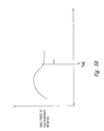
- FIG. 8 is a schematic cross-sectional view of the planarizing machine of FIG. 7 along line 8 — 8 .
- FIG. 9 is a schematic cross-sectional view of a planarizing machine in accordance with another embodiment of the invention.
- FIG. 10 is a schematic cross-sectional view of a planarizing machine in accordance with still another embodiment of the invention.
- FIG. 12 is a schematic isometric view of a rotary planarizing machine with a cut-away section illustrating an endpointing apparatus in accordance with another embodiment of the invention.
- FIG. 13 is a schematic cross-sectional view of the planarizing machine of FIG. 12 taken along line 13 — 13 .
- FIG. 14 is a schematic cross-sectional view of a substrate holder having an endpointing apparatus in accordance with yet another embodiment of the invention.
- the present invention relates to planarizing machines and methods for monitoring and controlling planarizing processes in mechanical or chemical-mechanical planarization of microelectronic substrate assemblies.
- Many specific details of the invention are described below with reference to planarizing semiconductor wafers using web-format and rotary planarizing machines to provide a thorough understanding of such embodiments.
- general aspects of a representative web-format planarizing machine and illustrative methods for controlling CMP processing using this machine are initially described below.
- planarizing machines for practicing methods in accordance with the invention are then described.
- the present invention may have additional embodiments and/or can be practiced without several of the details described in the following description.
- FIG. 2 is a schematic cross-sectional view of a web-format planarizing machine 100 having a monitoring system for monitoring and controlling planarization of a microelectronic substrate assembly 12 in accordance with the invention.
- the planarizing machine 100 includes a table 110 , a carrier assembly 130 over the table 110 , and a polishing pad 140 on the table 110 .
- the carrier assembly 130 and the polishing pad 140 can be substantially the same as those describe above with reference to FIG. 1 .
- the polishing pad 140 is accordingly coupled to a pad-advancing mechanism having a plurality of rollers 120 , 121 , 122 and 123 .
- the pad-advancing mechanism can also be the same as that described above with reference to FIG. 1 .
- the planarizing machine 100 also includes a monitoring system that measures the drag force between the substrate assembly 12 and the polishing pad 140 during planarization to endpoint or control other aspects of the CMP process.
- the monitoring system can include a drag force measuring assembly 160 (identified by reference numbers 160 a and 160 b ), a processor 199 a coupled to the drag force measuring assembly 160 , and a database 199 b coupled to the processor 199 a.
- the drag force measuring assembly 160 measures a parameter that accurately indicates the drag force at the interface between the pad 140 and the substrate assembly 12 .
- the drag force measuring assembly 160 sends signals to the processor 199 a corresponding to the measured drag forces, and the processor 199 a calculates the total work exerted at the pad/substrate assembly interface from the drag force measurements.
- the processor 199 a also correlates the total work exerted at the pad/substrate assembly interface with a predetermined correlation between work and substrate assembly thickness stored in the database 199 b to determine an estimated substrate assembly thickness.
- the monitoring system uses the estimated substrate assembly thickness and the elapsed time to endpoint CMP processing or provide other diagnostic information.
- the drag force measuring assembly 160 can be coupled to the table 110 and/or a carrier head 132 of the carrier assembly 130 .
- the drag force measuring assembly 160 is generally configured to isolate a drag force parameter indicative of drag force between the substrate assembly 12 and the polishing pad 140 that is not influenced by energy losses in motors, gears or other components that drive either the polishing pad 140 or the carrier head 132 .
- the drag force parameter can be lateral displacement between components of the table 110 and/or the carrier head 132 corresponding to a shear force between the substrate assembly 12 and the planarizing surface 142 of the polishing pad 140 .
- the drag force measuring assembly 160 includes at least one force detector 190 (shown schematically) that periodically measures the isolated drag force parameter and produces a signal corresponding to the measured drag forces.
- the processor 199 a processes the signals of the measured drag forces from the force detector 190 to determine the work exerted at the pad/substrate interface. As explained in greater detail below, the processor 199 a can integrate the measured drag forces over time to determine an estimated work performed at the pad/substrate assembly interface. Several methods for controlling or endpointing CMP processing using the calculated value of the estimated work are set forth below.
- FIG. 3 is a flowchart of a method for endpointing CMP processing of the substrate assembly 12 in accordance with one embodiment of the invention.
- the method illustrated in FIG. 3 is a comprehensive method that includes several procedures that may be combined with each other or completely excluded in other embodiments of the invention. Accordingly, other embodiments of the invention may also include different procedures or a different order of procedures.
- the CMP process of FIG. 3 is applicable to several different types of semiconductor wafers, field emission displays and other microelectronic substrate assemblies.
- the planarizing process illustrated in FIG. 3 includes removing material from a substrate assembly by pressing the substrate assembly against a planarizing surface (procedure 410 ) and moving the substrate assembly and/or the polishing pad with respect to the other (procedure 412 ).
- the polishing pad can be the web-format pad 140 shown in FIG. 2 or a rotary pad.
- the polishing pad can also be a fixed-abrasive pad with abrasive particles fixedly attached to a suspension medium or a non-abrasive pad without abrasive particles.
- the substrate assembly is generally pressed against the polishing pad in the presence of a planarizing solution.
- FIGS. 4A and 4B are schematic cross-sectional views illustrating the removal of material from two different types of substrate assemblies 12 a and 12 b in greater detail.
- the substrate assemblies 12 a and 12 b contact the planarizing surface 142 of the polishing pad 140 at a pad/substrate interface 143 defined by the surface area “SA” in contact with the planarizing surface 142 .
- the carrier assembly 130 presses the substrate assembly 12 a against the planarizing surface 142 at a downforce F d .
- the carrier assembly 130 also moves the substrate assembly 12 a with respect to the polishing pad 140 to rub the substrate assembly 12 a against the planarizing surface 142 at a relative velocity V r .
- the friction between the substrate assembly 12 a and the planarizing surface 142 creates a drag force F D that acts against the polishing pad 140 .
- FIG. 4A more specifically, illustrates a blanket oxide CMP process in which the substrate assembly 12 a has a substrate 13 a, a plurality of features 14 a, and a blanket oxide layer 16 composed of doped or undoped silicon dioxide.
- FIG. 4B illustrates a Shallow-Trench-Isolation (“STI”) planarizing process in which the substrate assembly 12 b has a substrate 13 b with a plurality of trenches 14 b, a polish-stop layer 15 b composed of a first material with a low polishing rate, and a fill layer 16 b composed of a second material having a high polishing rate relative to the polish-stop layer 15 b.
- STI Shallow-Trench-Isolation
- the polish-stop layer 15 b can be a layer of silicon nitride or carbon, and the fill layer 16 b can be a layer of doped or undoped silicon dioxide.
- the different underlying structures and layers of the substrate assemblies 12 a and 12 b produce different drag forces F D at the pad/substrate interface 143 , and thus the remaining procedures of the process shown in FIG. 3 are generally specific to each type of substrate assembly.
- the planarizing process 400 continues with a measuring procedure 420 that includes measuring a drag force parameter indicative of the drag force F D between the substrate assembly 12 and the polishing pad 140 .
- the drag force parameter is generally isolated from energy losses in components that drive either the polishing pad or the substrate assembly to provide a more accurate indication of the drag force F D at the pad/substrate interface 143 (FIG. 4 A).
- FIGS. 5A and 5B are graphs of the measured drag force F D at the pad/substrate interface over time.
- FIG. 5A more specifically, illustrates the drag force at the pad/substrate interface for a blanket oxide substrate assembly similar to the substrate assembly 12 a shown in FIG. 4 A.
- FIG. 5B illustrates the drag force at the pad/substrate interface for an STI substrate assembly similar to the substrate assembly 12 b shown in FIG. 4 B.
- FIGS. 5A and 5B illustrate that different types of substrate assemblies produce different drag forces at the pad/substrate interface.
- the area under each plot may also change for different runs of the same type of substrate assembly because input variables, such as pad condition, may change over time.
- the data processing procedure 430 can thus include integrating the mathematical product of the measured drag force F D and the relative velocity V r over time to determine the estimated work exerted at the pad/substrate interface 143 .
- the data processing procedure can include integrating the measured drag force F D over time (dt) to determine the magnitude of the total drag force exerted against the substrate assembly 12 during the planarizing cycle.
- the data processing procedure 430 of integrating the product of the measured drag force F D and the relative velocity V r over time to determine the estimated work can be performed by computer software or hardware using the trapezoidal method. Suitable software programs and hardware for performing the data processing procedure 430 are commercially available and generally known to those skilled in semiconductor manufacturing arts.
- the method 400 of FIG. 3 also includes a determining procedure 440 to determine an association between the work exerted at the pad/substrate interface and the change in substrate assembly thickness.
- the present inventors discovered that the change in thickness of the substrate assembly varies linearly with the work performed at the pad/substrate interface.
- a straight-line correlation between the change in substrate assembly thickness and work can be determined empirically for each type of substrate structure by planarizing a specific substrate assembly for a period of time, measuring the actual change in thickness of the substrate assembly, and calculating the estimated work exerted at the pad/substrate interface according to the measuring procedure 420 and the data processing procedure 430 described above with reference to FIGS. 4-5B.
- the method 400 of FIG. 3 continues with a correlating procedure 450 in which the estimated work at the pad/substrate interface is correlated with the linear association between the work and substrate assembly thickness to ascertain an estimated substrate thickness.
- the processor 199 a inputs the estimated work into the straight-line equation correlating work and change in substrate thickness to calculate the estimated substrate thickness.
- the planarizing process 400 further includes an endpointing procedure 460 that terminates removal of material from the substrate assembly by removing the substrate assembly 12 from the polishing pad 140 when the estimated change in substrate thickness (e.g., the thickness of material removed from the substrate assembly by planarization) is at least approximately within a range of a desired substrate assembly thickness for endpointing the substrate assembly.
- the method 400 of FIG. 3 can include different embodiments for determining the estimated change in thickness of a substrate assembly for a complete planarizing cycle or only a selected portion of the planarizing cycle.
- the entire area under the drag force versus time relationship for the blanket oxide CMP of the substrate assembly 12 a (FIG. 4A) can be integrated to determine an estimated work.
- This particular embodiment accordingly determines an estimate of the total change in thickness of the blanket oxide substrate assembly 12 a during the planarizing cycle.
- FIG. 4B the STI substrate assembly 12 b
- FIGS. 7-14 illustrate several embodiments of endpointing apparatuses that execute the measuring procedure 420 (FIG. 3) by isolating a drag force parameter related to the drag force between the substrate assembly 12 and the polishing pad 140 from other energy losses, and measuring the isolated drag force during planarization.
- the endpointing apparatuses described in FIGS. 7-14 define one type of drag force measuring assembly 160 shown in FIG. 2 . Therefore, it will be understood that the drag force measured with the endpointing apparatuses shown in FIGS. 7-14 can also be used to diagnose or control other aspects of the CMP processes described above with reference to FIGS. 2-6.
- FIG. 7 is a schematic isometric view of the web-format planarizing machine 100 including an endpointing apparatus for measuring the drag force between the substrate assembly 12 and the polishing pad 140 during planarization.
- the endpointing apparatus generally includes a secondary support member defined by a sub-platen 150 , a primary support member defined by a platen 170 , and at least one force detector 190 between the sub-platen 150 and the platen 170 .
- the platen 170 and the sub-platen 150 can be separate components of the table 110 .
- the polishing pad 140 is releasably coupled to the platen 170 so that the drag forces F D between the substrate assembly 12 and the pad 140 exert lateral forces against the platen 170 independent of friction losses or power losses in the carrier assembly 130 .
- the lateral force exerted by the pad 140 against the platen 170 is thus an isolated parameter indicative of the drag F D between the substrate assembly 12 and the pad 140 .
- FIG. 8 is a schematic cross-sectional view of the planarizing machine 100 illustrating the endpointing apparatus in greater detail.
- the sub-platen 150 can be a base supporting the platen 170 .
- the sub-platen 150 has a recess 152 defined by a base surface 153 and a plurality of walls (identified by reference numbers 154 a, 154 b, 156 a and 156 b ) projecting upwardly from the base surface 153 transversely with respect to a planarizing plane P—P (FIG. 8 ).
- the term “transverse” means any non-parallel arrangement and is not limited to a perpendicular arrangement.
- the walls can include a first side-wall 154 a, a second side-wall 154 b opposite the first side-wall 154 a, a first end-wall 156 a at one end of the side-walls 154 a and 154 b, and a second end-wall 156 b at the other end of the side-walls 154 a and 154 b.
- the walls can be configured in a rectilinear pattern or other suitable patterns to receive the platen 170 .
- the platen 170 is positioned in the recess 152 of the sub-platen 150 .
- the platen 170 can be a plate having a first side-face 172 a, a second side-face 172 b opposite the first side-face 172 a, a first end-face 174 a between one end of the side-faces 172 a and 172 b, and a second end-face 174 b between the other end of the side-faces 172 a and 172 b.
- the platen 170 also includes a bearing surface 176 facing the backside of the polishing pad 140 to support at least a portion of the polishing pad 140 in a planarizing zone under the head 132 .
- the platen 170 further includes a back surface 178 facing the base surface 153 of the sub-platen 150 .
- the polishing pad 140 is coupled to the bearing surface 176 during planarization so that the pad transmits lateral forces to the platen 170 .
- Suitable devices and methods for coupling the polishing pad 140 to the bearing surface 176 are disclosed in U.S. patent application Ser. Nos. 09/285,319 filed on Apr. 2, 1999, and 09/181,578 filed on Oct. 28, 1998, both of which are herein incorporated by reference.
- the bearing assembly 180 can also be a low-friction coating or lubricant between the base surface 153 and the back surface 178 , or a flexible bladder (not shown) between the sub-platen 150 and the platen 170 .
- the bearing assembly 180 can be a frictionless device having a number of air bearings defined by air holes through the sub-platen 150 that are connected to a pressurized air source that provides a continuous layer of air between the sub-platen 150 and the platen 170 .
- the bearing assembly 180 can be a magnetic device including magnetic bearings that prevent the back surface 178 from contacting the base surface 153 by positioning magnetic fields of a like polarity adjacent to one another. In operation, the bearing assembly 180 can frictionally isolate the platen 170 from the sub-platen 150 so that the drag forces between the substrate assembly 12 and the pad 140 drive the platen 170 laterally with respect to the sub-platen 150 without substantial friction losses.
- the force detectors 190 can be other sensors that generate electrical signals corresponding to the lateral forces or displacement between the sub-platen 150 and the platen 170 .
- the force detectors 190 can be lasers, accelerometers, capacitance displacement sensors, linear variable differential transformers or other displacement sensors.
- planarizing machine 100 In the particular embodiment of the planarizing machine 100 illustrated in FIGS. 7 and 8, four force detectors are configured along two orthogonal axes. In other embodiments, the planarizing machine 100 can have only one force detector positioned along one axis, or two force detectors positioned along two orthogonal axes, or any number of force detectors positioned between the walls of the sub-platen 150 and the faces of the platen 170 .
- first and second force detectors 190 a and 190 b can be positioned as explained above, and the dead stops or force detectors 190 c and 190 d can be eliminated by sizing the platen 170 such that the second end-face 174 b abuts the second end-wall 156 b and the second side-face 172 b abuts the second sidewall 154 b.
- FIG. 9 is a schematic cross-sectional view of the planarizing machine 100 in accordance with another embodiment of the invention.
- the sub-platen 150 has a post 155 projecting upwardly from the base surface 153 , and the platen 170 is fixedly attached to the post 155 .
- the walls 172 / 174 of the platen 170 do not contact either dead stops, the faces 154 / 156 of the sub-platen 150 , or other devices that inhibit the platen 170 from moving with respect to the sub-platen 150 .
- the force detector 190 can be a strain gauge attached to the post 155 to measure the torsional displacement of the post 155 , a laser or other type of displacement sensor. The force detector 190 accordingly senses the change in the displacement of the torsional forces exerted on the platen 170 and sends a corresponding signal to the processor 199 a.
- FIG. 10 is a schematic cross-sectional view of the planarizing machine 100 in accordance with another embodiment of the invention in which a number of small posts 155 attach the platen 170 to the sub-platen 150 .
- the walls 172 / 174 of the platen 170 do not contact either dead stops, the faces 154 / 156 of the sub-platen 150 , or other devices that inhibit the platen 170 from moving with respect to the sub-platen 150 .
- the posts 155 can be threaded studs having a diameter of approximately 1.0 inch and a length of 3.0 inches made from metal, high density polymers or other suitable materials.
- the posts 155 can also be other supports that can flex more in one direction than others, and the posts 155 can be made from other materials.
- the posts 155 of this embodiment accordingly do not frictionally isolate the platen 170 from the sub-platen 150 , but rather they deflect to control the motion between the platen 170 and the sub-platen 150 in correspondence to the drag forces between the substrate assembly 12 and the polishing pad 140 .
- the force detectors 190 accordingly measure the displacement between the platen 170 and the sub-platen 150 to determine the drag forces between the substrate assembly 12 and the polishing pad 140 .
- FIG. 11 is a schematic isometric view of a planarizing machine 100 in accordance with still another embodiment of the invention.
- the planarizing machine 100 has a circular platen 170 and the recess 152 in the sub-platen 150 has a single circular wall 154 .
- the platen 170 accordingly has a single, circular side-face 174 .
- the platen 170 can be coupled to the sub-platen 150 by any of the bearings 180 or posts 155 described above with reference to FIGS. 7-10.
- FIG. 12 is a schematic isometric view of a planarizing machine 200 in accordance with another embodiment of the invention
- FIG. 13 is a schematic cross-sectional view of the planarizing machine 200 in FIG. 12 taken along line 13 — 13
- the planarizing machine 200 has a sub-platen 250 coupled to a rotary drive mechanism 251 to rotate the sub-platen 250 (arrow R), a platen 270 movably coupled to the sub-platen 250 , and a polishing pad 240 attached to the platen 270 .
- the sub-platen 250 has a base surface 253 facing the polishing pad 240 and a tab 254 projecting upwardly from the base surface 253 .
- the tab 254 has a stop surface 256 facing in the direction of the rotation of the sub-platen 250 .
- the platen 270 includes an opening 271 having a contact surface 272 facing the stop surface 256 of the tab 254 .
- the planarizing machine 200 further includes a bearing assembly 280 that can be the same as the bearing assembly 180 described above with reference to FIG. 8 .
- the planarizing machine 200 also includes a force detector 290 contacting the stop surface 256 of the tab 254 and the contact surface 272 of the platen 270 .
- the planarizing machine 200 is expected to enhance the accuracy of detecting the endpoint of planarizing a substrate assembly in rotary planarizing applications.
- a carrier assembly 230 moves a carrier head 232 to press the substrate assembly 12 against a planarizing surface 242 of the polishing pad 240 .
- the rotary drive assembly 251 also rotates the sub-platen 250 causing the tab 254 to press the force detector 290 against the contact surface 272 .
- the sub-platen 250 accordingly rotates the platen 270 in the direction R, but the drag force between the substrate assembly 12 and the polishing pad 240 resists rotation in the direction R.
- the bearing assembly 280 allows the drag forces between the substrate assembly 12 and the planarizing surface 242 to drive the contact surface 272 of the platen 270 against the force detector 290 in correlation to the drag forces.
- the force detector 290 accordingly detects an increase in the lateral force that the platen 270 exerts against the tab 254 .
- the force detector 290 is coupled to a processor 299 to convert the signals from the force detector 290 into data that can be analyzed to determine the endpoint of the planarizing process as described above with reference to FIGS. 2-6.
- FIG. 14 is a schematic cross-sectional view of a carrier system 330 for a planarizing machine in accordance with another embodiment of the invention.
- the carrier assembly 330 can include a carrier head 332 having a lower portion 333 with a lower cavity 334 to receive a substrate assembly 12 and an upper portion 336 with an upper cavity 338 .
- a pivoting joint 350 is attached to the head 332 in the cavity 338 , and a drive-shaft 339 is pivotally attached to the joint 350 .
- the endpointing apparatus includes a primary support member defined by the head 332 , a secondary support member defined by the drive-shaft 339 , and a first contact surface defined by the side-wall of the upper cavity 338 .
- the joint 350 is a gimbal joint or other bearing assembly that allows universal pivoting between the head 332 and the shaft 339 .
- the carrier head 332 also includes a force detector 390 attached to an interior wall of the cavity 338 .
- the force detector 390 can be an annular piezoelectric ring.
- the drag forces between the substrate assembly 12 and the polishing pad 140 cause the shaft 339 to pivot about the joint 350 such that the lower end of the shaft 339 contacts the force detector 390 .
- the force exerted by the driveshaft 339 against the force detector 390 will be proportional to the drag forces between the substrate assembly 12 and the polishing pad 140 .
- the isolated drag force parameter of this embodiment is the displacement between the shaft 339 and the carrier head 332 .
- the force detector 390 is coupled to a processor 199 a (FIG. 2) to detect the endpoint of the planarizing process in a manner similar to that described above with respect to FIGS. 2-6.
- planarizing machines and methods described above with reference to FIGS. 2-14 are expected to enhance the accuracy of endpointing CMP processing compared to processes and devices that monitor changes in the current of the drive motors.
- the methods described above with reference to FIGS. 2-6 for example, accurately endpoint CMP processing because they use the work exerted at the pad/substrate interface as the determinative value for estimating the endpoint.
- One aspect of these methods is that the inventors discovered a linear correlation between work at the pad/substrate interface and the change in thickness of the substrate assembly. Moreover, the work-thickness correlation is not affected by changes in the condition of the polishing pad, agglomerations of abrasive particles in the slurry, or other mechanical factors.
- the estimated work determined according to the embodiments set forth above with respect to FIGS. 2-6 accordingly provides an accurate estimate of the change in thickness of the substrate assembly during a planarizing cycle irrespective of changes in mechanical variables.
- several embodiments of the methods described above with reference to FIGS. 2-6 can accurately endpoint CMP processing even though mechanical input variables change over time.
- planarizing machines described above with reference to FIGS. 2 and 7 - 14 are further expected to enhance the accuracy of endpointing CMP processing because they isolate a drag force parameter that is not influenced by energy losses unrelated to the drag force at the pad/substrate interface.
- several embodiments of the planarizing machines described above with reference to FIGS. 7-14 measure the drag force between the substrate assembly and the polishing pad by isolating the displacement or the lateral forces between either a platen and sub-platen, or a carrier head and a drive shaft.
- the isolated drag force parameter provides a much more accurate indication of the actual drag force at the pad/substrate interface than measuring motor current because energy losses and other factors associated with moving the carrier head or the polishing pad do not influence or otherwise overshadow the changes in drag force between the pad and the substrate assembly.
- the endpointing apparatuses and monitoring systems described above with reference to FIGS. 7-14, therefore, are expected to enhance the accuracy of detecting the endpoint in CMP processing.
- the methods described above with reference to FIGS. 2-6 are also expected to enhance the accuracy of controlling and diagnosing CMP processing.
- Another aspect of several embodiments of the methods described above with reference to FIGS. 2-6 is that the source of unexpected problems in CMP processing can be diagnosed. Because the chemistry of the planarizing solution only changes the slope of the work/thickness relationship shown in FIG. 6, the source of an unexpected result in a specific run of wafers can be more readily identified.
- unexpected results in the finished substrate assemblies can generally be attributed to changes in the chemical interaction between the planarizing solution and the substrate assembly because endpointing CMP processing by determining the estimate work at the pad/substrate interface is not influenced by mechanical variables. Therefore, by determining the estimated work at the pad/substrate interface, unexpected changes in chemical aspects of CMP processing can be more readily diagnosed.
Abstract
Description
Claims (18)
Priority Applications (1)
| Application Number | Priority Date | Filing Date | Title |
|---|---|---|---|
| US10/139,299 US6682628B2 (en) | 1999-08-31 | 2002-05-02 | Methods and apparatuses for monitoring and controlling mechanical or chemical-mechanical planarization of microelectronic substrate assemblies |
Applications Claiming Priority (2)
| Application Number | Priority Date | Filing Date | Title |
|---|---|---|---|
| US09/386,648 US6464824B1 (en) | 1999-08-31 | 1999-08-31 | Methods and apparatuses for monitoring and controlling mechanical or chemical-mechanical planarization of microelectronic substrate assemblies |
| US10/139,299 US6682628B2 (en) | 1999-08-31 | 2002-05-02 | Methods and apparatuses for monitoring and controlling mechanical or chemical-mechanical planarization of microelectronic substrate assemblies |
Related Parent Applications (1)
| Application Number | Title | Priority Date | Filing Date |
|---|---|---|---|
| US09/386,648 Division US6464824B1 (en) | 1999-08-31 | 1999-08-31 | Methods and apparatuses for monitoring and controlling mechanical or chemical-mechanical planarization of microelectronic substrate assemblies |
Publications (2)
| Publication Number | Publication Date |
|---|---|
| US20020124957A1 US20020124957A1 (en) | 2002-09-12 |
| US6682628B2 true US6682628B2 (en) | 2004-01-27 |
Family
ID=23526474
Family Applications (2)
| Application Number | Title | Priority Date | Filing Date |
|---|---|---|---|
| US09/386,648 Expired - Lifetime US6464824B1 (en) | 1999-08-31 | 1999-08-31 | Methods and apparatuses for monitoring and controlling mechanical or chemical-mechanical planarization of microelectronic substrate assemblies |
| US10/139,299 Expired - Lifetime US6682628B2 (en) | 1999-08-31 | 2002-05-02 | Methods and apparatuses for monitoring and controlling mechanical or chemical-mechanical planarization of microelectronic substrate assemblies |
Family Applications Before (1)
| Application Number | Title | Priority Date | Filing Date |
|---|---|---|---|
| US09/386,648 Expired - Lifetime US6464824B1 (en) | 1999-08-31 | 1999-08-31 | Methods and apparatuses for monitoring and controlling mechanical or chemical-mechanical planarization of microelectronic substrate assemblies |
Country Status (1)
| Country | Link |
|---|---|
| US (2) | US6464824B1 (en) |
Cited By (3)
| Publication number | Priority date | Publication date | Assignee | Title |
|---|---|---|---|---|
| US20060224158A1 (en) * | 2005-03-31 | 2006-10-05 | Darren Odom | Electrosurgical forceps with slow closure sealing plates and method of sealing tissue |
| US20100330878A1 (en) * | 2004-06-21 | 2010-12-30 | Yoichi Kobayashi | Polishing apparatus and polishing method |
| US10705000B2 (en) * | 2017-11-21 | 2020-07-07 | Fanuc Corporation | Tool-life determination device |
Families Citing this family (22)
| Publication number | Priority date | Publication date | Assignee | Title |
|---|---|---|---|---|
| US6492273B1 (en) * | 1999-08-31 | 2002-12-10 | Micron Technology, Inc. | Methods and apparatuses for monitoring and controlling mechanical or chemical-mechanical planarization of microelectronic substrate assemblies |
| US20020016136A1 (en) * | 2000-06-16 | 2002-02-07 | Manoocher Birang | Conditioner for polishing pads |
| US6605159B2 (en) * | 2001-08-30 | 2003-08-12 | Micron Technology, Inc. | Device and method for collecting and measuring chemical samples on pad surface in CMP |
| US6939198B1 (en) * | 2001-12-28 | 2005-09-06 | Applied Materials, Inc. | Polishing system with in-line and in-situ metrology |
| US6869498B1 (en) * | 2002-02-04 | 2005-03-22 | Applied Materials, Inc. | Chemical mechanical polishing with shear force measurement |
| US20030199112A1 (en) | 2002-03-22 | 2003-10-23 | Applied Materials, Inc. | Copper wiring module control |
| US7087527B2 (en) * | 2002-08-28 | 2006-08-08 | Micron Technology, Inc. | Extended kalman filter incorporating offline metrology |
| US6827635B2 (en) * | 2003-03-05 | 2004-12-07 | Infineon Technologies Aktiengesellschaft | Method of planarizing substrates |
| US6932674B2 (en) * | 2003-03-05 | 2005-08-23 | Infineon Technologies Aktientgesellschaft | Method of determining the endpoint of a planarization process |
| TWI275451B (en) * | 2005-01-11 | 2007-03-11 | Asia Ic Mic Process Inc | Measurement of thickness profile and elastic modulus profile of polishing pad |
| US8260446B2 (en) | 2005-08-22 | 2012-09-04 | Applied Materials, Inc. | Spectrographic monitoring of a substrate during processing using index values |
| CN100449703C (en) * | 2006-08-11 | 2009-01-07 | 中芯国际集成电路制造(上海)有限公司 | Method for controlling chemical and mechanical grinding endpoint |
| US20110282477A1 (en) * | 2010-05-17 | 2011-11-17 | Applied Materials, Inc. | Endpoint control of multiple substrates with multiple zones on the same platen in chemical mechanical polishing |
| US9308618B2 (en) * | 2012-04-26 | 2016-04-12 | Applied Materials, Inc. | Linear prediction for filtering of data during in-situ monitoring of polishing |
| CN108291036A (en) | 2015-12-01 | 2018-07-17 | 金伯利-克拉克环球有限公司 | Include the absorbability and protective composite of elastomer copolymer |
| US10043970B2 (en) * | 2016-12-15 | 2018-08-07 | Taiwan Semiconductor Manufacturing Co., Ltd. | Determining a characteristic of a monitored layer on an integrated chip |
| JP6948878B2 (en) * | 2017-08-22 | 2021-10-13 | ラピスセミコンダクタ株式会社 | Semiconductor manufacturing equipment and semiconductor substrate polishing method |
| US11504821B2 (en) | 2017-11-16 | 2022-11-22 | Applied Materials, Inc. | Predictive filter for polishing pad wear rate monitoring |
| WO2019177842A1 (en) | 2018-03-12 | 2019-09-19 | Applied Materials, Inc. | Filtering during in-situ monitoring of polishing |
| US20200035495A1 (en) * | 2018-07-25 | 2020-01-30 | Globalfoundries Inc. | Chemical-mechanical polishing with variable-pressure polishing pads |
| US11570849B2 (en) * | 2018-12-06 | 2023-01-31 | Schneider Electric Systems Usa, Inc. | Wireless instrument area network node with internal force sensor |
| US11282755B2 (en) | 2019-08-27 | 2022-03-22 | Applied Materials, Inc. | Asymmetry correction via oriented wafer loading |
Citations (11)
| Publication number | Priority date | Publication date | Assignee | Title |
|---|---|---|---|---|
| US4351029A (en) * | 1979-12-05 | 1982-09-21 | Westinghouse Electric Corp. | Tool life monitoring and tracking apparatus |
| US5036015A (en) | 1990-09-24 | 1991-07-30 | Micron Technology, Inc. | Method of endpoint detection during chemical/mechanical planarization of semiconductor wafers |
| US5069002A (en) * | 1991-04-17 | 1991-12-03 | Micron Technology, Inc. | Apparatus for endpoint detection during mechanical planarization of semiconductor wafers |
| US5216843A (en) * | 1992-09-24 | 1993-06-08 | Intel Corporation | Polishing pad conditioning apparatus for wafer planarization process |
| US5245794A (en) * | 1992-04-09 | 1993-09-21 | Advanced Micro Devices, Inc. | Audio end point detector for chemical-mechanical polishing and method therefor |
| US5308438A (en) * | 1992-01-30 | 1994-05-03 | International Business Machines Corporation | Endpoint detection apparatus and method for chemical/mechanical polishing |
| US5337015A (en) * | 1993-06-14 | 1994-08-09 | International Business Machines Corporation | In-situ endpoint detection method and apparatus for chemical-mechanical polishing using low amplitude input voltage |
| US5595526A (en) * | 1994-11-30 | 1997-01-21 | Intel Corporation | Method and apparatus for endpoint detection in a chemical/mechanical process for polishing a substrate |
| US5738562A (en) * | 1996-01-24 | 1998-04-14 | Micron Technology, Inc. | Apparatus and method for planar end-point detection during chemical-mechanical polishing |
| US6206754B1 (en) * | 1999-08-31 | 2001-03-27 | Micron Technology, Inc. | Endpoint detection apparatus, planarizing machines with endpointing apparatus, and endpointing methods for mechanical or chemical-mechanical planarization of microelectronic substrate assemblies |
| US6306008B1 (en) * | 1999-08-31 | 2001-10-23 | Micron Technology, Inc. | Apparatus and method for conditioning and monitoring media used for chemical-mechanical planarization |
-
1999
- 1999-08-31 US US09/386,648 patent/US6464824B1/en not_active Expired - Lifetime
-
2002
- 2002-05-02 US US10/139,299 patent/US6682628B2/en not_active Expired - Lifetime
Patent Citations (13)
| Publication number | Priority date | Publication date | Assignee | Title |
|---|---|---|---|---|
| US4351029A (en) * | 1979-12-05 | 1982-09-21 | Westinghouse Electric Corp. | Tool life monitoring and tracking apparatus |
| US5036015A (en) | 1990-09-24 | 1991-07-30 | Micron Technology, Inc. | Method of endpoint detection during chemical/mechanical planarization of semiconductor wafers |
| US5069002A (en) * | 1991-04-17 | 1991-12-03 | Micron Technology, Inc. | Apparatus for endpoint detection during mechanical planarization of semiconductor wafers |
| US5308438A (en) * | 1992-01-30 | 1994-05-03 | International Business Machines Corporation | Endpoint detection apparatus and method for chemical/mechanical polishing |
| US5245794A (en) * | 1992-04-09 | 1993-09-21 | Advanced Micro Devices, Inc. | Audio end point detector for chemical-mechanical polishing and method therefor |
| US5216843A (en) * | 1992-09-24 | 1993-06-08 | Intel Corporation | Polishing pad conditioning apparatus for wafer planarization process |
| US5337015A (en) * | 1993-06-14 | 1994-08-09 | International Business Machines Corporation | In-situ endpoint detection method and apparatus for chemical-mechanical polishing using low amplitude input voltage |
| US5595526A (en) * | 1994-11-30 | 1997-01-21 | Intel Corporation | Method and apparatus for endpoint detection in a chemical/mechanical process for polishing a substrate |
| US5738562A (en) * | 1996-01-24 | 1998-04-14 | Micron Technology, Inc. | Apparatus and method for planar end-point detection during chemical-mechanical polishing |
| US6206754B1 (en) * | 1999-08-31 | 2001-03-27 | Micron Technology, Inc. | Endpoint detection apparatus, planarizing machines with endpointing apparatus, and endpointing methods for mechanical or chemical-mechanical planarization of microelectronic substrate assemblies |
| US6306008B1 (en) * | 1999-08-31 | 2001-10-23 | Micron Technology, Inc. | Apparatus and method for conditioning and monitoring media used for chemical-mechanical planarization |
| US6364746B2 (en) * | 1999-08-31 | 2002-04-02 | Micron Technology, Inc. | Endpoint detection apparatus, planarizing machines with endpointing apparatus, and endpointing methods for mechanical or chemical-mechanical planarization of microelectronic-substrate assemblies |
| US6572440B2 (en) * | 1999-08-31 | 2003-06-03 | Micron Technology, Inc. | Apparatus and method for conditioning and monitoring media used for chemical-mechanical planarization |
Non-Patent Citations (2)
| Title |
|---|
| Ferdinand P. Beer and E. Russell Johnston, Jr., Statics and Dynamics, 5<th >Ed. 1988, McGraw-Hill, p. 841. |
| Ferdinand P. Beer and E. Russell Johnston, Jr., Statics and Dynamics, 5th Ed. 1988, McGraw-Hill, p. 841. |
Cited By (4)
| Publication number | Priority date | Publication date | Assignee | Title |
|---|---|---|---|---|
| US20100330878A1 (en) * | 2004-06-21 | 2010-12-30 | Yoichi Kobayashi | Polishing apparatus and polishing method |
| US8112169B2 (en) * | 2004-06-21 | 2012-02-07 | Ebara Corporation | Polishing apparatus and polishing method |
| US20060224158A1 (en) * | 2005-03-31 | 2006-10-05 | Darren Odom | Electrosurgical forceps with slow closure sealing plates and method of sealing tissue |
| US10705000B2 (en) * | 2017-11-21 | 2020-07-07 | Fanuc Corporation | Tool-life determination device |
Also Published As
| Publication number | Publication date |
|---|---|
| US20020124957A1 (en) | 2002-09-12 |
| US6464824B1 (en) | 2002-10-15 |
Similar Documents
| Publication | Publication Date | Title |
|---|---|---|
| US7625495B2 (en) | Methods and apparatuses for monitoring and controlling mechanical or chemical-mechanical planarization of microelectronic substrate assemblies | |
| US6682628B2 (en) | Methods and apparatuses for monitoring and controlling mechanical or chemical-mechanical planarization of microelectronic substrate assemblies | |
| US6364746B2 (en) | Endpoint detection apparatus, planarizing machines with endpointing apparatus, and endpointing methods for mechanical or chemical-mechanical planarization of microelectronic-substrate assemblies | |
| US6350180B2 (en) | Methods for predicting polishing parameters of polishing pads, and methods and machines for planarizing microelectronic substrate assemblies in mechanical or chemical-mechanical planarization | |
| US7182668B2 (en) | Methods for analyzing and controlling performance parameters in mechanical and chemical-mechanical planarization of microelectronic substrates | |
| US6007408A (en) | Method and apparatus for endpointing mechanical and chemical-mechanical polishing of substrates | |
| US7235000B2 (en) | Methods and systems for conditioning planarizing pads used in planarizing substrates | |
| US20020037681A1 (en) | Method and apparatus for controlled polishing | |
| US20060199472A1 (en) | Apparatus and method for conditioning a polishing pad used for mechanical and/or chemical-mechanical planarization | |
| US6194231B1 (en) | Method for monitoring polishing pad used in chemical-mechanical planarization process | |
| US20060196283A1 (en) | Measurement of Thickness Profile and Elastic Modulus Profile of a Polishing Pad | |
| WO2001032360A1 (en) | Closed-loop ultrasonic conditioning control for polishing pads |
Legal Events
| Date | Code | Title | Description |
|---|---|---|---|
| FEPP | Fee payment procedure |
Free format text: PAYOR NUMBER ASSIGNED (ORIGINAL EVENT CODE: ASPN); ENTITY STATUS OF PATENT OWNER: LARGE ENTITY |
|
| STCF | Information on status: patent grant |
Free format text: PATENTED CASE |
|
| CC | Certificate of correction | ||
| FPAY | Fee payment |
Year of fee payment: 4 |
|
| FPAY | Fee payment |
Year of fee payment: 8 |
|
| FPAY | Fee payment |
Year of fee payment: 12 |
|
| AS | Assignment |
Owner name: U.S. BANK NATIONAL ASSOCIATION, AS COLLATERAL AGENT, CALIFORNIA Free format text: SECURITY INTEREST;ASSIGNOR:MICRON TECHNOLOGY, INC.;REEL/FRAME:038669/0001 Effective date: 20160426 Owner name: U.S. BANK NATIONAL ASSOCIATION, AS COLLATERAL AGEN Free format text: SECURITY INTEREST;ASSIGNOR:MICRON TECHNOLOGY, INC.;REEL/FRAME:038669/0001 Effective date: 20160426 |
|
| AS | Assignment |
Owner name: MORGAN STANLEY SENIOR FUNDING, INC., AS COLLATERAL AGENT, MARYLAND Free format text: PATENT SECURITY AGREEMENT;ASSIGNOR:MICRON TECHNOLOGY, INC.;REEL/FRAME:038954/0001 Effective date: 20160426 Owner name: MORGAN STANLEY SENIOR FUNDING, INC., AS COLLATERAL Free format text: PATENT SECURITY AGREEMENT;ASSIGNOR:MICRON TECHNOLOGY, INC.;REEL/FRAME:038954/0001 Effective date: 20160426 |
|
| AS | Assignment |
Owner name: U.S. BANK NATIONAL ASSOCIATION, AS COLLATERAL AGENT, CALIFORNIA Free format text: CORRECTIVE ASSIGNMENT TO CORRECT THE REPLACE ERRONEOUSLY FILED PATENT #7358718 WITH THE CORRECT PATENT #7358178 PREVIOUSLY RECORDED ON REEL 038669 FRAME 0001. ASSIGNOR(S) HEREBY CONFIRMS THE SECURITY INTEREST;ASSIGNOR:MICRON TECHNOLOGY, INC.;REEL/FRAME:043079/0001 Effective date: 20160426 Owner name: U.S. BANK NATIONAL ASSOCIATION, AS COLLATERAL AGEN Free format text: CORRECTIVE ASSIGNMENT TO CORRECT THE REPLACE ERRONEOUSLY FILED PATENT #7358718 WITH THE CORRECT PATENT #7358178 PREVIOUSLY RECORDED ON REEL 038669 FRAME 0001. ASSIGNOR(S) HEREBY CONFIRMS THE SECURITY INTEREST;ASSIGNOR:MICRON TECHNOLOGY, INC.;REEL/FRAME:043079/0001 Effective date: 20160426 |
|
| AS | Assignment |
Owner name: JPMORGAN CHASE BANK, N.A., AS COLLATERAL AGENT, ILLINOIS Free format text: SECURITY INTEREST;ASSIGNORS:MICRON TECHNOLOGY, INC.;MICRON SEMICONDUCTOR PRODUCTS, INC.;REEL/FRAME:047540/0001 Effective date: 20180703 Owner name: JPMORGAN CHASE BANK, N.A., AS COLLATERAL AGENT, IL Free format text: SECURITY INTEREST;ASSIGNORS:MICRON TECHNOLOGY, INC.;MICRON SEMICONDUCTOR PRODUCTS, INC.;REEL/FRAME:047540/0001 Effective date: 20180703 |
|
| AS | Assignment |
Owner name: MICRON TECHNOLOGY, INC., IDAHO Free format text: RELEASE BY SECURED PARTY;ASSIGNOR:U.S. BANK NATIONAL ASSOCIATION, AS COLLATERAL AGENT;REEL/FRAME:047243/0001 Effective date: 20180629 |
|
| AS | Assignment |
Owner name: MICRON TECHNOLOGY, INC., IDAHO Free format text: RELEASE BY SECURED PARTY;ASSIGNOR:MORGAN STANLEY SENIOR FUNDING, INC., AS COLLATERAL AGENT;REEL/FRAME:050937/0001 Effective date: 20190731 |
|
| AS | Assignment |
Owner name: MICRON SEMICONDUCTOR PRODUCTS, INC., IDAHO Free format text: RELEASE BY SECURED PARTY;ASSIGNOR:JPMORGAN CHASE BANK, N.A., AS COLLATERAL AGENT;REEL/FRAME:051028/0001 Effective date: 20190731 Owner name: MICRON TECHNOLOGY, INC., IDAHO Free format text: RELEASE BY SECURED PARTY;ASSIGNOR:JPMORGAN CHASE BANK, N.A., AS COLLATERAL AGENT;REEL/FRAME:051028/0001 Effective date: 20190731 |