US6677668B1 - Configuration for testing a substrate mounted with a most performance-demanding integrated circuit - Google Patents
Configuration for testing a substrate mounted with a most performance-demanding integrated circuit Download PDFInfo
- Publication number
- US6677668B1 US6677668B1 US09/727,913 US72791300A US6677668B1 US 6677668 B1 US6677668 B1 US 6677668B1 US 72791300 A US72791300 A US 72791300A US 6677668 B1 US6677668 B1 US 6677668B1
- Authority
- US
- United States
- Prior art keywords
- chip
- substrate
- performance
- demanding
- csp
- Prior art date
- Legal status (The legal status is an assumption and is not a legal conclusion. Google has not performed a legal analysis and makes no representation as to the accuracy of the status listed.)
- Expired - Fee Related, expires
Links
Images


Classifications
-
- H—ELECTRICITY
- H01—ELECTRIC ELEMENTS
- H01L—SEMICONDUCTOR DEVICES NOT COVERED BY CLASS H10
- H01L24/00—Arrangements for connecting or disconnecting semiconductor or solid-state bodies; Methods or apparatus related thereto
- H01L24/80—Methods for connecting semiconductor or other solid state bodies using means for bonding being attached to, or being formed on, the surface to be connected
- H01L24/81—Methods for connecting semiconductor or other solid state bodies using means for bonding being attached to, or being formed on, the surface to be connected using a bump connector
-
- B—PERFORMING OPERATIONS; TRANSPORTING
- B23—MACHINE TOOLS; METAL-WORKING NOT OTHERWISE PROVIDED FOR
- B23K—SOLDERING OR UNSOLDERING; WELDING; CLADDING OR PLATING BY SOLDERING OR WELDING; CUTTING BY APPLYING HEAT LOCALLY, e.g. FLAME CUTTING; WORKING BY LASER BEAM
- B23K3/00—Tools, devices, or special appurtenances for soldering, e.g. brazing, or unsoldering, not specially adapted for particular methods
- B23K3/06—Solder feeding devices; Solder melting pans
- B23K3/0607—Solder feeding devices
- B23K3/0623—Solder feeding devices for shaped solder piece feeding, e.g. preforms, bumps, balls, pellets, droplets
-
- H—ELECTRICITY
- H01—ELECTRIC ELEMENTS
- H01L—SEMICONDUCTOR DEVICES NOT COVERED BY CLASS H10
- H01L23/00—Details of semiconductor or other solid state devices
- H01L23/48—Arrangements for conducting electric current to or from the solid state body in operation, e.g. leads, terminal arrangements ; Selection of materials therefor
- H01L23/488—Arrangements for conducting electric current to or from the solid state body in operation, e.g. leads, terminal arrangements ; Selection of materials therefor consisting of soldered or bonded constructions
- H01L23/498—Leads, i.e. metallisations or lead-frames on insulating substrates, e.g. chip carriers
- H01L23/49811—Additional leads joined to the metallisation on the insulating substrate, e.g. pins, bumps, wires, flat leads
- H01L23/49816—Spherical bumps on the substrate for external connection, e.g. ball grid arrays [BGA]
-
- H—ELECTRICITY
- H05—ELECTRIC TECHNIQUES NOT OTHERWISE PROVIDED FOR
- H05K—PRINTED CIRCUITS; CASINGS OR CONSTRUCTIONAL DETAILS OF ELECTRIC APPARATUS; MANUFACTURE OF ASSEMBLAGES OF ELECTRICAL COMPONENTS
- H05K3/00—Apparatus or processes for manufacturing printed circuits
- H05K3/30—Assembling printed circuits with electric components, e.g. with resistor
- H05K3/32—Assembling printed circuits with electric components, e.g. with resistor electrically connecting electric components or wires to printed circuits
- H05K3/34—Assembling printed circuits with electric components, e.g. with resistor electrically connecting electric components or wires to printed circuits by soldering
- H05K3/341—Surface mounted components
- H05K3/3431—Leadless components
- H05K3/3436—Leadless components having an array of bottom contacts, e.g. pad grid array or ball grid array components
-
- B—PERFORMING OPERATIONS; TRANSPORTING
- B23—MACHINE TOOLS; METAL-WORKING NOT OTHERWISE PROVIDED FOR
- B23K—SOLDERING OR UNSOLDERING; WELDING; CLADDING OR PLATING BY SOLDERING OR WELDING; CUTTING BY APPLYING HEAT LOCALLY, e.g. FLAME CUTTING; WORKING BY LASER BEAM
- B23K2101/00—Articles made by soldering, welding or cutting
- B23K2101/36—Electric or electronic devices
- B23K2101/40—Semiconductor devices
-
- H—ELECTRICITY
- H01—ELECTRIC ELEMENTS
- H01L—SEMICONDUCTOR DEVICES NOT COVERED BY CLASS H10
- H01L2224/00—Indexing scheme for arrangements for connecting or disconnecting semiconductor or solid-state bodies and methods related thereto as covered by H01L24/00
- H01L2224/01—Means for bonding being attached to, or being formed on, the surface to be connected, e.g. chip-to-package, die-attach, "first-level" interconnects; Manufacturing methods related thereto
- H01L2224/10—Bump connectors; Manufacturing methods related thereto
- H01L2224/11—Manufacturing methods
- H01L2224/113—Manufacturing methods by local deposition of the material of the bump connector
- H01L2224/1133—Manufacturing methods by local deposition of the material of the bump connector in solid form
- H01L2224/11334—Manufacturing methods by local deposition of the material of the bump connector in solid form using preformed bumps
-
- H—ELECTRICITY
- H01—ELECTRIC ELEMENTS
- H01L—SEMICONDUCTOR DEVICES NOT COVERED BY CLASS H10
- H01L2224/00—Indexing scheme for arrangements for connecting or disconnecting semiconductor or solid-state bodies and methods related thereto as covered by H01L24/00
- H01L2224/01—Means for bonding being attached to, or being formed on, the surface to be connected, e.g. chip-to-package, die-attach, "first-level" interconnects; Manufacturing methods related thereto
- H01L2224/10—Bump connectors; Manufacturing methods related thereto
- H01L2224/12—Structure, shape, material or disposition of the bump connectors prior to the connecting process
- H01L2224/13—Structure, shape, material or disposition of the bump connectors prior to the connecting process of an individual bump connector
- H01L2224/13001—Core members of the bump connector
- H01L2224/13099—Material
- H01L2224/131—Material with a principal constituent of the material being a metal or a metalloid, e.g. boron [B], silicon [Si], germanium [Ge], arsenic [As], antimony [Sb], tellurium [Te] and polonium [Po], and alloys thereof
- H01L2224/13101—Material with a principal constituent of the material being a metal or a metalloid, e.g. boron [B], silicon [Si], germanium [Ge], arsenic [As], antimony [Sb], tellurium [Te] and polonium [Po], and alloys thereof the principal constituent melting at a temperature of less than 400°C
- H01L2224/13111—Tin [Sn] as principal constituent
-
- H—ELECTRICITY
- H01—ELECTRIC ELEMENTS
- H01L—SEMICONDUCTOR DEVICES NOT COVERED BY CLASS H10
- H01L2224/00—Indexing scheme for arrangements for connecting or disconnecting semiconductor or solid-state bodies and methods related thereto as covered by H01L24/00
- H01L2224/80—Methods for connecting semiconductor or other solid state bodies using means for bonding being attached to, or being formed on, the surface to be connected
- H01L2224/81—Methods for connecting semiconductor or other solid state bodies using means for bonding being attached to, or being formed on, the surface to be connected using a bump connector
- H01L2224/818—Bonding techniques
- H01L2224/81801—Soldering or alloying
-
- H—ELECTRICITY
- H01—ELECTRIC ELEMENTS
- H01L—SEMICONDUCTOR DEVICES NOT COVERED BY CLASS H10
- H01L2924/00—Indexing scheme for arrangements or methods for connecting or disconnecting semiconductor or solid-state bodies as covered by H01L24/00
- H01L2924/0001—Technical content checked by a classifier
- H01L2924/00014—Technical content checked by a classifier the subject-matter covered by the group, the symbol of which is combined with the symbol of this group, being disclosed without further technical details
-
- H—ELECTRICITY
- H01—ELECTRIC ELEMENTS
- H01L—SEMICONDUCTOR DEVICES NOT COVERED BY CLASS H10
- H01L2924/00—Indexing scheme for arrangements or methods for connecting or disconnecting semiconductor or solid-state bodies as covered by H01L24/00
- H01L2924/01—Chemical elements
- H01L2924/01019—Potassium [K]
-
- H—ELECTRICITY
- H01—ELECTRIC ELEMENTS
- H01L—SEMICONDUCTOR DEVICES NOT COVERED BY CLASS H10
- H01L2924/00—Indexing scheme for arrangements or methods for connecting or disconnecting semiconductor or solid-state bodies as covered by H01L24/00
- H01L2924/01—Chemical elements
- H01L2924/01029—Copper [Cu]
-
- H—ELECTRICITY
- H01—ELECTRIC ELEMENTS
- H01L—SEMICONDUCTOR DEVICES NOT COVERED BY CLASS H10
- H01L2924/00—Indexing scheme for arrangements or methods for connecting or disconnecting semiconductor or solid-state bodies as covered by H01L24/00
- H01L2924/01—Chemical elements
- H01L2924/01033—Arsenic [As]
-
- H—ELECTRICITY
- H01—ELECTRIC ELEMENTS
- H01L—SEMICONDUCTOR DEVICES NOT COVERED BY CLASS H10
- H01L2924/00—Indexing scheme for arrangements or methods for connecting or disconnecting semiconductor or solid-state bodies as covered by H01L24/00
- H01L2924/01—Chemical elements
- H01L2924/01082—Lead [Pb]
-
- H—ELECTRICITY
- H01—ELECTRIC ELEMENTS
- H01L—SEMICONDUCTOR DEVICES NOT COVERED BY CLASS H10
- H01L2924/00—Indexing scheme for arrangements or methods for connecting or disconnecting semiconductor or solid-state bodies as covered by H01L24/00
- H01L2924/013—Alloys
- H01L2924/014—Solder alloys
-
- H—ELECTRICITY
- H01—ELECTRIC ELEMENTS
- H01L—SEMICONDUCTOR DEVICES NOT COVERED BY CLASS H10
- H01L2924/00—Indexing scheme for arrangements or methods for connecting or disconnecting semiconductor or solid-state bodies as covered by H01L24/00
- H01L2924/10—Details of semiconductor or other solid state devices to be connected
- H01L2924/11—Device type
- H01L2924/14—Integrated circuits
-
- H—ELECTRICITY
- H05—ELECTRIC TECHNIQUES NOT OTHERWISE PROVIDED FOR
- H05K—PRINTED CIRCUITS; CASINGS OR CONSTRUCTIONAL DETAILS OF ELECTRIC APPARATUS; MANUFACTURE OF ASSEMBLAGES OF ELECTRICAL COMPONENTS
- H05K2201/00—Indexing scheme relating to printed circuits covered by H05K1/00
- H05K2201/10—Details of components or other objects attached to or integrated in a printed circuit board
- H05K2201/10613—Details of electrical connections of non-printed components, e.g. special leads
- H05K2201/10621—Components characterised by their electrical contacts
- H05K2201/10674—Flip chip
-
- H—ELECTRICITY
- H05—ELECTRIC TECHNIQUES NOT OTHERWISE PROVIDED FOR
- H05K—PRINTED CIRCUITS; CASINGS OR CONSTRUCTIONAL DETAILS OF ELECTRIC APPARATUS; MANUFACTURE OF ASSEMBLAGES OF ELECTRICAL COMPONENTS
- H05K2201/00—Indexing scheme relating to printed circuits covered by H05K1/00
- H05K2201/10—Details of components or other objects attached to or integrated in a printed circuit board
- H05K2201/10613—Details of electrical connections of non-printed components, e.g. special leads
- H05K2201/10621—Components characterised by their electrical contacts
- H05K2201/10719—Land grid array [LGA]
-
- H—ELECTRICITY
- H05—ELECTRIC TECHNIQUES NOT OTHERWISE PROVIDED FOR
- H05K—PRINTED CIRCUITS; CASINGS OR CONSTRUCTIONAL DETAILS OF ELECTRIC APPARATUS; MANUFACTURE OF ASSEMBLAGES OF ELECTRICAL COMPONENTS
- H05K2203/00—Indexing scheme relating to apparatus or processes for manufacturing printed circuits covered by H05K3/00
- H05K2203/04—Soldering or other types of metallurgic bonding
- H05K2203/041—Solder preforms in the shape of solder balls
-
- H—ELECTRICITY
- H05—ELECTRIC TECHNIQUES NOT OTHERWISE PROVIDED FOR
- H05K—PRINTED CIRCUITS; CASINGS OR CONSTRUCTIONAL DETAILS OF ELECTRIC APPARATUS; MANUFACTURE OF ASSEMBLAGES OF ELECTRICAL COMPONENTS
- H05K3/00—Apparatus or processes for manufacturing printed circuits
- H05K3/30—Assembling printed circuits with electric components, e.g. with resistor
- H05K3/32—Assembling printed circuits with electric components, e.g. with resistor electrically connecting electric components or wires to printed circuits
- H05K3/34—Assembling printed circuits with electric components, e.g. with resistor electrically connecting electric components or wires to printed circuits by soldering
- H05K3/3457—Solder materials or compositions; Methods of application thereof
- H05K3/3473—Plating of solder
-
- Y—GENERAL TAGGING OF NEW TECHNOLOGICAL DEVELOPMENTS; GENERAL TAGGING OF CROSS-SECTIONAL TECHNOLOGIES SPANNING OVER SEVERAL SECTIONS OF THE IPC; TECHNICAL SUBJECTS COVERED BY FORMER USPC CROSS-REFERENCE ART COLLECTIONS [XRACs] AND DIGESTS
- Y02—TECHNOLOGIES OR APPLICATIONS FOR MITIGATION OR ADAPTATION AGAINST CLIMATE CHANGE
- Y02P—CLIMATE CHANGE MITIGATION TECHNOLOGIES IN THE PRODUCTION OR PROCESSING OF GOODS
- Y02P70/00—Climate change mitigation technologies in the production process for final industrial or consumer products
- Y02P70/50—Manufacturing or production processes characterised by the final manufactured product
-
- Y—GENERAL TAGGING OF NEW TECHNOLOGICAL DEVELOPMENTS; GENERAL TAGGING OF CROSS-SECTIONAL TECHNOLOGIES SPANNING OVER SEVERAL SECTIONS OF THE IPC; TECHNICAL SUBJECTS COVERED BY FORMER USPC CROSS-REFERENCE ART COLLECTIONS [XRACs] AND DIGESTS
- Y10—TECHNICAL SUBJECTS COVERED BY FORMER USPC
- Y10T—TECHNICAL SUBJECTS COVERED BY FORMER US CLASSIFICATION
- Y10T428/00—Stock material or miscellaneous articles
- Y10T428/24—Structurally defined web or sheet [e.g., overall dimension, etc.]
- Y10T428/24802—Discontinuous or differential coating, impregnation or bond [e.g., artwork, printing, retouched photograph, etc.]
- Y10T428/24917—Discontinuous or differential coating, impregnation or bond [e.g., artwork, printing, retouched photograph, etc.] including metal layer
Definitions
- This invention relates generally to the electronic package. More particularly, this invention relates to a new and improved manufacture process by first selecting a known good substrate (KGS) by first testing a substrate mounted with a most performance-demanding chip before testing and mounting additional multiple chips onto the substrate.
- KGS known good substrate
- MCM multiple-chip module
- FIGS. 1A to 1 D for a top view of a substrate and a top view, side cross sectional view and bottom view respectively of a conventional MCM assembly that includes three IC chips.
- FIG. 1E is a flow chart for illustrating the process flow for manufacturing the MCM assembly shown in FIGS. 1A to 1 C.
- the MCM substrate supports the interconnecting traces and the ball grid array as that shown in FIG. 1C is manufactured.
- the first, second, and third IC chips are mounted onto the substrate, with a top view shown in FIG. 1B, using a chip on board (COB) process.
- COB chip on board
- standard wire bonding processes are carried out for packaging direct-attached multiple chips and the substrate.
- an encapsulation is applied to cover multiple chips and to protect the bonding wires under the encapsulation.
- a burn-in and functional tests are performed to determine whether the MCM assembly would pass or fail the tests.
- failure of the substrate or anyone of the multiple chips can lead to the failure of the MCM assembly.
- Employment of a substrate without actual functional test as now commonly implemented in the manufacturing process of the MCM assemblies can therefore cause significant reduction of production yield, particularly when there are more stringent requirements now imposed on the performance of the substrate as well as on the chips.
- FIG. 1F is a flow chart of showing another process flow by first assembling, burning testing each of the multiple chips as chip size package (CSP). These tested and known-good CSP chips are then mounted on a substrate provided with BGA or a land-grid array.
- CSP chip size package
- This process is most costly and production can be improved by assuring only known good dies are employed. This method however can still be impacted by using a substrate due to the fact that the substrate is untested and probably cannot achieve the performance requirements with higher speed and packaging density are now required for the MCM assembly.
- MCMs multiple chip modules
- the substrate is provided for first mounting a most performance-demanding chip and then using a set of footprints formed on the substrate for clamping remainder of multiple chips for carrying out a functional MCM test to assure the substrate is working properly.
- the functionality and performance of the substrate can be more realistic tested before the final MCM assembly is manufactured and tested. The problems encountered by the prior art in using an untested substrate are therefore resolved.
- the present invention comprises a substrate having a top surface for mounting multiple integrated circuit (IC) chips.
- the substrate includes a first footprint comprising a plurality of electrical contacts disposed on the top surface for mounting a most performance-demanding IC chip thereon.
- the substrate further includes a set of substrate testing footprints comprising a plurality of package mounting and testing electrical contacts for temporarily mounting a plurality of testing packages to conduct a functional MCM test for the substrate mounted with the most performance-demanding IC chip and the testing packages.
- the substrate further includes a plurality of solder balls disposed on a bottom surface of the substrate opposite the top surface.
- the substrate further includes a plurality interconnecting traces interconnected between the electrical contacts of the first footprint and the set of substrate testing footprints.
- the first footprint for mounting the most performance-demanding IC chip includes a plurality of electrical contacts arranged for wire-bonding the most performance-demanding IC chip onto the substrate.
- the first footprint for mounting the most performance-demanding IC chip includes a plurality of electrical contacts arranged for disposing a packaged IC chip as the most performance-demanding IC chip onto the substrate.
- the set of substrate testing footprints comprising at least a set of chip-size package (CSP) electrical contacts for temporarily mounting at least a CSP testing package to conduct a functional MCM test for the substrate mounted with the most performance-demanding IC chip and the testing packages.
- the set of substrate testing footprints comprising at least a set of flip chip package (FCP) electrical contacts for temporarily mounting at least a flip-chip testing package to conduct a functional MCM test for the substrate mounted with the most performance-demanding IC chip and the testing packages.
- CSP chip-size package
- FCP flip chip package
- the set of substrate testing footprints comprising at least a set of signal generator electrical contacts for temporarily mounting at least a signal generator to conduct a functional MCM test for the substrate mounted with the most performance-demanding IC chip and the testing packages.
- the first footprint for mounting the most performance-demanding IC chip includes a plurality of electrical contacts arranged for mounting the most performance-demanding IC chip as a chip-size package onto the substrate.
- the first footprint for mounting the most performance-demanding IC chip includes a plurality of electrical contacts arranged for mounting the most performance-demanding IC chip as a flip-chip package onto the substrate.
- FIGS. 1A to 1 D show a top view of a substrate, a top view, a cross sectional view and bottom view respectively of a MCM assembly manufactured with a conventional method
- FIGS. 1E and 1F are two flowcharts for illustrating the process flow implemented in two alternate conventional processes for manufacturing a MCM assembly
- FIGS. 2A to 2 C show a top view, a cross sectional view and a bottom view respectively of a MCM assembly manufactured with a new and improved method disclosed in this invention
- FIG. 3 is a flow chart for illustrating the new and improved process flow for manufacturing a MCM assembly of this invention
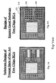
- FIG. 4A is a top view of a substrate of this invention ready for mounting a most performance-demanding chip applying a regular COB process and two sets of CSP footprints for mounting two CSP packaged chip;
- FIG. 4B is a top view of a substrate of this invention shown two testing packages such as a known good flip chip and a CSP chip for carrying out a MCM functional test with the substrate before final mounting of the remainder of the multiple chips;
- FIGS. 5A and 5B are a top view and a cross sectional view of another MCM assembly of this invention.
- FIGS. 2A to 2 C for a top view, cross sectional view and a bottom view respectively for a MCM assembly manufactured by a new and improved process of this invention as illustrated in FIG. 3 .
- the process begins with a step of mounting a first integrated circuit (IC) chip 120 , e.g., die #1, onto a substrate 110 that has a footprint shown in FIG. 4A for mounting the IC chip 120 with a chip-on-board (COB) applying a wire-bonding process.
- the top view of the substrate 110 as that shown in FIG. 4A also provides two chip-size package (CSP) footprints 130 and 140 for the purpose of testing and mounting known good CSP chips or flip chip on these footprints to be further discussed below.
- CSP chip-size package
- a preferred embodiment is to mount a most performance-demanding chip 120 on the substrate 110 .
- a top view of the substrate 110 is shown in FIG. 4A that is formed with a plurality of interconnecting traces 135 interconnected between electric contacts for the IC chip 120 and electric contacts of peripheral IC chips.
- a bottom view of the substrate 110 is shown in FIG. 2 C.
- the substrate is provided with a plurality of solder balls 180 formed as a ball grid array (BGA).
- the most performance-demanding chip 120 typically is a processor chip that is mounted on the substrate 120 by applying a direct chip attachment (DCA) configuration and then wire bonded to the substrate 110 with bonding wires 115 .
- DCA direct chip attachment
- the mounted and wire-bonded chip 120 is then encapsulated with an encapsulation layer 125 .
- a burn-in test is performed on the encapsulated chip 120 now assembled to the substrate 110 (step 220 ) to assure that the substrate together with the encapsulated chip 120 , e.g., the most performance-demanding chip, are qualified through the burn-in tests.
- FIG. 4B for a top view of the substrate 120 mounted with the first chip 120 and having two sets of CSP footprints 130 and 140 .
- a substrate testing process is performed by clamping on two know good chips that can either be a flip chip or a CSP chip (step 230 ). These two test packages 160 and 170 can also be implemented with signal generators for performing a substrate testing.
- a full functional test (step 240 ) is then carried out to assure the most performance-demanding chip 120 mounted on the substrate 110 working together with the remainder of the multiple chips, e.g., chips 160 and 170 , can satisfy the functional requirements. The test would assure that the requirements according the specifications of the total and final MCM assembly are now satisfied based on test of the assembly formed in a near-realistic configuration.
- the second and third chips preferably known good dies (KGD), e.g., CSP #2 and CSP #3, are burned in and tested Step 250 ), and mounted onto the substrate 110 to complete the final MCM test (step 260 ).
- KGD known good dies
- a multiple chip module (MCM) supported on a substrate having a top surface for mounting multiple integrated circuit (IC) chips is disclosed in this invention.
- the MCM includes a first IC chip mounted on the top surface of the substrate.
- the MCM further includes a set of substrate testing footprints comprising a plurality of package mounting and testing electrical contacts for temporarily mounting a plurality of testing packages to conduct a functional MCM test for the substrate mounted with the first IC chip and the testing packages.
- the MCM further includes an encapsulation for encapsulating the first IC chip.
- the first IC chip is a most performance-demanding chip among the multiple IC chips.
- the MCM further includes a plurality of solder balls disposed on a bottom surface of the substrate opposite the top surface.
- the MCM further includes a plurality interconnecting traces interconnected between electrical contacts connected to the first IC chip and the electric contacts of the set of substrate testing footprints.
- the first IC chip encapsulated in the encapsulation is mounted onto the substrate with a wire-bonding configuration.
- the first IC chip is a chip-size package IC chip mounted onto the substrate.
- the first IC chip is a flip-chip package IC chip mounted onto the substrate.
- the set of substrate testing footprints comprising at least a set of chip-size package (CSP) electrical contacts for temporarily mounting at least a CSP testing package to conduct a functional MCM test for the substrate mounted with the first IC chip and the testing packages.
- the set of substrate testing footprints comprising at least a set of flip-chip package (CSP) electrical contacts for temporarily mounting at least a flip-chip testing package to conduct a functional MCM test for the substrate mounted with the first IC chip and the testing packages.
- the set of substrate testing footprints comprising at least a set of signal generator electrical contacts for temporarily mounting at least a signal generator to conduct a functional MCM test for the substrate mounted with the first IC chip and the testing packages.
- the substrate further includes a first footprint for mounting the first IC chip and the first footprint includes a plurality of electrical contacts arranged for mounting the first IC chip as a chip-size package onto the substrate.
- the MCM further includes a first footprint for mounting the first IC chip and the first footprint includes a plurality of electrical contacts arranged for mounting the first IC chip as a flip-chip package onto the substrate.
- FIG. 5 shows another preferred embodiment with a most performance-demanding IC chip 320 disposed in the center of the top surface of a substrate 310 .
- the most performance-demanding IC chip 320 is first wire-bonded to the substrate 310 with bonding wires 315 and encapsulated with an encapsulation 325 .
- Four test packages are then mounted on a set of four footprints 330 - 1 to 330 - 4 to perform a MCM functional test (step 240 ) to assure the substrate can function properly to satisfy all the functional specification of the MCM performance requirements.
- Four known-good packaged IC chips include at least one flip chip 360 and one chip-size package IC chip are then mounted on the footprints to complete the final MCM test (step 260 ).
- the MCM assembly is further provided with solder balls 380 formed as BGA array on the bottom surface of the substrate 310 for further mounting and connecting to external circuit board.
- This invention further discloses a method for mounting multiple integrated circuit (IC) chips on a top surface of a substrate.
- the method includes a step of forming a fist footprint to include a plurality of electrical contacts on the top surface for mounting a most performance-demanding IC chip thereon.
- the method further includes a step of forming a set of substrate testing footprints to include a plurality of package mounting and testing electrical contacts for temporarily mounting a plurality of testing packages to conduct a functional MCM test for the substrate.
- the substrate under test is mounted with the most performance-demanding IC chip and the testing packages.
- the method further includes a step of forming a plurality of solder balls on a bottom surface of the substrate opposite the top surface.
- the method further includes a step of forming a plurality interconnecting traces for interconnecting the electrical contacts of the first footprint and the set of substrate testing footprints.
- the method further includes a step of forming the first footprint for mounting the most performance-demanding IC chip includes a step of forming a plurality of electrical contacts arranged for wire-bonding the most performance-demanding IC chip onto the substrate.
- the step of forming the first footprint for mounting the most performance-demanding IC chip includes a step of forming a plurality of electrical contacts arranged for disposing a packaged IC chip as the most performance demanding IC chip onto the substrate.
- the step of forming the set of substrate testing footprints comprising a step of forming at least a set of chip-size package (CSP) electrical contacts for temporarily mounting at least a CSP testing package to conduct a functional MCM test for the substrate mounted with the most performance-demanding IC chip and the testing packages.
- the step of forming the set of substrate testing footprints comprising a step of forming at least a set of flip-chip package (CSP) electrical contacts for temporarily mounting at least a flip-chip testing package to conduct a functional MCM test for the substrate mounted with the most performance-demanding IC chip and the testing packages.
- CSP chip-size package
- the step of forming the set of substrate testing footprints comprising a step of forming at least a set of signal generator electrical contacts for temporarily mounting at least a signal generator to conduct a functional MCM test for the substrate mounted with the most performance-demanding IC chip and the testing packages.
- the step of forming the first footprint for mounting the most performance-demanding IC chip includes a step of forming a plurality of electrical contacts arranged for mounting the most performance-demanding IC chip as a chip-size package onto the substrate.
- the step of forming the first footprint for mounting the most performance-demanding IC chip includes a step of forming a plurality of electrical contacts arranged for mounting the most performance-demanding IC chip as a flip-chip package onto the substrate.
Abstract
Description
Claims (10)
Priority Applications (1)
| Application Number | Priority Date | Filing Date | Title |
|---|---|---|---|
| US09/727,913 US6677668B1 (en) | 1998-01-13 | 2000-11-28 | Configuration for testing a substrate mounted with a most performance-demanding integrated circuit |
Applications Claiming Priority (3)
| Application Number | Priority Date | Filing Date | Title |
|---|---|---|---|
| US7117798P | 1998-01-13 | 1998-01-13 | |
| US09/229,139 US6369451B2 (en) | 1998-01-13 | 1999-01-12 | Solder balls and columns with stratified underfills on substrate for flip chip joining |
| US09/727,913 US6677668B1 (en) | 1998-01-13 | 2000-11-28 | Configuration for testing a substrate mounted with a most performance-demanding integrated circuit |
Related Parent Applications (1)
| Application Number | Title | Priority Date | Filing Date |
|---|---|---|---|
| US09/229,139 Continuation-In-Part US6369451B2 (en) | 1998-01-13 | 1999-01-12 | Solder balls and columns with stratified underfills on substrate for flip chip joining |
Publications (1)
| Publication Number | Publication Date |
|---|---|
| US6677668B1 true US6677668B1 (en) | 2004-01-13 |
Family
ID=26751935
Family Applications (1)
| Application Number | Title | Priority Date | Filing Date |
|---|---|---|---|
| US09/727,913 Expired - Fee Related US6677668B1 (en) | 1998-01-13 | 2000-11-28 | Configuration for testing a substrate mounted with a most performance-demanding integrated circuit |
Country Status (1)
| Country | Link |
|---|---|
| US (1) | US6677668B1 (en) |
Cited By (12)
| Publication number | Priority date | Publication date | Assignee | Title |
|---|---|---|---|---|
| US20040012934A1 (en) * | 2002-07-16 | 2004-01-22 | Behdad Jafari | Multi-configuration processor-memory substrate device |
| US20040121515A1 (en) * | 2002-09-23 | 2004-06-24 | David Kautz | Programmable multi-chip module |
| US20040195700A1 (en) * | 2003-04-04 | 2004-10-07 | Advanced Semiconductor Engineering Inc. | Multi-chip package combining wire-bonding and flip-chip configuration |
| US6818838B1 (en) * | 2003-03-17 | 2004-11-16 | Unisys Corporation | PCB component placement and trace routing therebetween |
| US20050014397A1 (en) * | 2003-07-15 | 2005-01-20 | Alcatel | Tailored interconnect module |
| US20060255460A1 (en) * | 2005-05-12 | 2006-11-16 | Endicott Interconnect Technologies, Inc. | Multi-chip electronic package with reduced line skew, method of making same and information handling system utilizing same |
| US20070090534A1 (en) * | 2005-10-20 | 2007-04-26 | Hironori Iwasaki | Semiconductor module including a plurality of IC chips therein |
| US20080012116A1 (en) * | 2006-07-13 | 2008-01-17 | Samsung Electronics Co., Ltd. | Semiconductor device and method of forming the same |
| US20080150088A1 (en) * | 2006-12-20 | 2008-06-26 | Reed Paul A | Method for incorporating existing silicon die into 3d integrated stack |
| CN1950939B (en) * | 2004-09-28 | 2010-05-05 | 罗姆股份有限公司 | Semiconductor device |
| US20130087911A1 (en) * | 2011-10-07 | 2013-04-11 | Mediatek Inc. | Integrated circuit package structure |
| US9507378B2 (en) | 2012-11-07 | 2016-11-29 | Nvidia Corporation | Flat panel electronic device, auxiliary heat-dissipating means thereof and assembly of both |
Citations (6)
| Publication number | Priority date | Publication date | Assignee | Title |
|---|---|---|---|---|
| US5754410A (en) * | 1996-09-11 | 1998-05-19 | International Business Machines Corporation | Multi-chip module with accessible test pads |
| US5757074A (en) * | 1995-07-07 | 1998-05-26 | Hughes Electronics Corporation | Microwave/millimeter wave circuit structure with discrete flip-chip mounted elements |
| US6064219A (en) * | 1997-02-05 | 2000-05-16 | Tektronix, Inc. | Modular test chip for multi chip module |
| US6246252B1 (en) * | 1999-07-30 | 2001-06-12 | Sun Microsystems, Inc. | Efficient debug package design |
| US6278286B1 (en) * | 1997-08-22 | 2001-08-21 | Micron Technology, Inc. | Interconnect and system for making temporary electrical connections to semiconductor components |
| US20020195704A1 (en) * | 2001-06-21 | 2002-12-26 | Vincent Chan | Multi-die module and method thereof |
-
2000
- 2000-11-28 US US09/727,913 patent/US6677668B1/en not_active Expired - Fee Related
Patent Citations (6)
| Publication number | Priority date | Publication date | Assignee | Title |
|---|---|---|---|---|
| US5757074A (en) * | 1995-07-07 | 1998-05-26 | Hughes Electronics Corporation | Microwave/millimeter wave circuit structure with discrete flip-chip mounted elements |
| US5754410A (en) * | 1996-09-11 | 1998-05-19 | International Business Machines Corporation | Multi-chip module with accessible test pads |
| US6064219A (en) * | 1997-02-05 | 2000-05-16 | Tektronix, Inc. | Modular test chip for multi chip module |
| US6278286B1 (en) * | 1997-08-22 | 2001-08-21 | Micron Technology, Inc. | Interconnect and system for making temporary electrical connections to semiconductor components |
| US6246252B1 (en) * | 1999-07-30 | 2001-06-12 | Sun Microsystems, Inc. | Efficient debug package design |
| US20020195704A1 (en) * | 2001-06-21 | 2002-12-26 | Vincent Chan | Multi-die module and method thereof |
Cited By (26)
| Publication number | Priority date | Publication date | Assignee | Title |
|---|---|---|---|---|
| US8264851B2 (en) | 2002-07-16 | 2012-09-11 | Nvidia Corporation | Multi-configuration processor-memory substrate device |
| US8837161B2 (en) * | 2002-07-16 | 2014-09-16 | Nvidia Corporation | Multi-configuration processor-memory substrate device |
| US20040012934A1 (en) * | 2002-07-16 | 2004-01-22 | Behdad Jafari | Multi-configuration processor-memory substrate device |
| US8482120B2 (en) | 2002-07-16 | 2013-07-09 | Nvidia Corporation | Combined heat sink multi-configuration processor memory substrate device |
| US20080106860A1 (en) * | 2002-07-16 | 2008-05-08 | Nvidia Corporation | Multi-configuration processor-memory substrate device |
| US20100103604A1 (en) * | 2002-07-16 | 2010-04-29 | Nvidia Corporation | Multi-configuration processor-memory substrate device |
| US20100103605A1 (en) * | 2002-07-16 | 2010-04-29 | Nvidia Corporation | multi-configuration processor-memory substrate device |
| US20080106861A1 (en) * | 2002-07-16 | 2008-05-08 | Behdad Jafari | Multi-configuration processor-memory substrate device |
| US20040121515A1 (en) * | 2002-09-23 | 2004-06-24 | David Kautz | Programmable multi-chip module |
| US6897078B2 (en) * | 2002-09-23 | 2005-05-24 | Honeywell Federal Manufacturing & Technologies | Programmable multi-chip module |
| US6818838B1 (en) * | 2003-03-17 | 2004-11-16 | Unisys Corporation | PCB component placement and trace routing therebetween |
| US20040195700A1 (en) * | 2003-04-04 | 2004-10-07 | Advanced Semiconductor Engineering Inc. | Multi-chip package combining wire-bonding and flip-chip configuration |
| US7081678B2 (en) * | 2003-04-04 | 2006-07-25 | Advanced Semiconductor Engineering Inc. | Multi-chip package combining wire-bonding and flip-chip configuration |
| US6908314B2 (en) * | 2003-07-15 | 2005-06-21 | Alcatel | Tailored interconnect module |
| US20050014397A1 (en) * | 2003-07-15 | 2005-01-20 | Alcatel | Tailored interconnect module |
| CN1950939B (en) * | 2004-09-28 | 2010-05-05 | 罗姆股份有限公司 | Semiconductor device |
| US7332818B2 (en) * | 2005-05-12 | 2008-02-19 | Endicott Interconnect Technologies, Inc. | Multi-chip electronic package with reduced line skew and circuitized substrate for use therein |
| US20060255460A1 (en) * | 2005-05-12 | 2006-11-16 | Endicott Interconnect Technologies, Inc. | Multi-chip electronic package with reduced line skew, method of making same and information handling system utilizing same |
| US20070090534A1 (en) * | 2005-10-20 | 2007-04-26 | Hironori Iwasaki | Semiconductor module including a plurality of IC chips therein |
| US7696615B2 (en) * | 2006-07-13 | 2010-04-13 | Samsung Electronics Co., Ltd. | Semiconductor device having pillar-shaped terminal |
| US20080012116A1 (en) * | 2006-07-13 | 2008-01-17 | Samsung Electronics Co., Ltd. | Semiconductor device and method of forming the same |
| US20080150088A1 (en) * | 2006-12-20 | 2008-06-26 | Reed Paul A | Method for incorporating existing silicon die into 3d integrated stack |
| US8110899B2 (en) * | 2006-12-20 | 2012-02-07 | Intel Corporation | Method for incorporating existing silicon die into 3D integrated stack |
| US20130087911A1 (en) * | 2011-10-07 | 2013-04-11 | Mediatek Inc. | Integrated circuit package structure |
| US9437512B2 (en) * | 2011-10-07 | 2016-09-06 | Mediatek Inc. | Integrated circuit package structure |
| US9507378B2 (en) | 2012-11-07 | 2016-11-29 | Nvidia Corporation | Flat panel electronic device, auxiliary heat-dissipating means thereof and assembly of both |
Similar Documents
| Publication | Publication Date | Title |
|---|---|---|
| US6512302B2 (en) | Apparatus and methods of packaging and testing die | |
| US10861824B2 (en) | Microelectronic device packages, stacked microelectronic device packages, and methods for manufacturing microelectronic devices | |
| US6249052B1 (en) | Substrate on chip (SOC) multiple-chip module (MCM) with chip-size-package (CSP) ready configuration | |
| US6301121B1 (en) | Direct-chip-attach (DCA) multiple chip module (MCM) with repair-chip ready site to simplify assembling and testing process | |
| US5998865A (en) | Loc simm | |
| US5763947A (en) | Integrated circuit chip package having configurable contacts and a removable connector | |
| US5534784A (en) | Method for probing a semiconductor wafer | |
| US4975765A (en) | Highly integrated circuit and method for the production thereof | |
| US6815251B1 (en) | High density modularity for IC's | |
| US6002178A (en) | Multiple chip module configuration to simplify testing process and reuse of known-good chip-size package (CSP) | |
| US7417322B2 (en) | Multi-chip module with embedded package and method for manufacturing the same | |
| US6680212B2 (en) | Method of testing and constructing monolithic multi-chip modules | |
| US6677668B1 (en) | Configuration for testing a substrate mounted with a most performance-demanding integrated circuit | |
| JPH0777556A (en) | Test receptacle and preparation of kgd using test receptacle | |
| US6133629A (en) | Multi-chip module package | |
| JP4616974B2 (en) | Multi-chip module packaging process | |
| US5243498A (en) | Multi-chip semiconductor module and method for making and testing | |
| US6628136B2 (en) | Method and apparatus for testing a semiconductor package | |
| US6433565B1 (en) | Test fixture for flip chip ball grid array circuits | |
| US7420206B2 (en) | Interposer, semiconductor chip mounted sub-board, and semiconductor package | |
| KR100378185B1 (en) | Micro ball grid array package tape including tap for testing | |
| WO1999026288A1 (en) | Semiconductor device and method for manufacturing the same | |
| US20040042189A1 (en) | Multi-chip integrated module | |
| JPH1167985A (en) | Semiconductor device | |
| JPS60200537A (en) | Semiconductor device with exclusive testing terminal |
Legal Events
| Date | Code | Title | Description |
|---|---|---|---|
| AS | Assignment |
Owner name: LIN PACKAGING TECHNOLOGIES, LTD., TEXAS Free format text: ASSIGNMENT OF ASSIGNORS INTEREST;ASSIGNOR:LIN, PAUL T.;REEL/FRAME:015931/0208 Effective date: 20050113 |
|
| FEPP | Fee payment procedure |
Free format text: PAT HOLDER NO LONGER CLAIMS SMALL ENTITY STATUS, ENTITY STATUS SET TO UNDISCOUNTED (ORIGINAL EVENT CODE: STOL); ENTITY STATUS OF PATENT OWNER: LARGE ENTITY |
|
| REFU | Refund |
Free format text: REFUND - SURCHARGE, PETITION TO ACCEPT PYMT AFTER EXP, UNINTENTIONAL (ORIGINAL EVENT CODE: R2551); ENTITY STATUS OF PATENT OWNER: LARGE ENTITY |
|
| FPAY | Fee payment |
Year of fee payment: 4 |
|
| SULP | Surcharge for late payment | ||
| FEPP | Fee payment procedure |
Free format text: PAYOR NUMBER ASSIGNED (ORIGINAL EVENT CODE: ASPN); ENTITY STATUS OF PATENT OWNER: LARGE ENTITY |
|
| AS | Assignment |
Owner name: PATENT BUSINESS DEVELOPMENT, LLC, FLORIDA Free format text: ASSIGNMENT OF ASSIGNORS INTEREST;ASSIGNOR:LIN PACKAGING TECHNOLOGIES, INC.;REEL/FRAME:025934/0013 Effective date: 20110125 |
|
| REMI | Maintenance fee reminder mailed | ||
| FPAY | Fee payment |
Year of fee payment: 8 |
|
| SULP | Surcharge for late payment |
Year of fee payment: 7 |
|
| AS | Assignment |
Owner name: CHIP PACKAGING SOLUTIONS LLC, TEXAS Free format text: ASSIGNMENT OF ASSIGNORS INTEREST;ASSIGNOR:ACACIA RESEARCH GROUP LLC;REEL/FRAME:030636/0181 Effective date: 20120210 Owner name: ACACIA RESEARCH GROUP LLC, TEXAS Free format text: ASSIGNMENT OF ASSIGNORS INTEREST;ASSIGNOR:PATENT BUSINESS DEVELOPMENT LLC;REEL/FRAME:030650/0472 Effective date: 20111216 |
|
| REMI | Maintenance fee reminder mailed | ||
| LAPS | Lapse for failure to pay maintenance fees | ||
| STCH | Information on status: patent discontinuation |
Free format text: PATENT EXPIRED DUE TO NONPAYMENT OF MAINTENANCE FEES UNDER 37 CFR 1.362 |
|
| FP | Lapsed due to failure to pay maintenance fee |
Effective date: 20160113 |