US6665187B1 - Thermally enhanced lid for multichip modules - Google Patents
Thermally enhanced lid for multichip modules Download PDFInfo
- Publication number
- US6665187B1 US6665187B1 US10/198,393 US19839302A US6665187B1 US 6665187 B1 US6665187 B1 US 6665187B1 US 19839302 A US19839302 A US 19839302A US 6665187 B1 US6665187 B1 US 6665187B1
- Authority
- US
- United States
- Prior art keywords
- lid
- coefficient
- expansion
- thermal expansion
- components
- Prior art date
- Legal status (The legal status is an assumption and is not a legal conclusion. Google has not performed a legal analysis and makes no representation as to the accuracy of the status listed.)
- Expired - Fee Related
Links
Images


Classifications
-
- H—ELECTRICITY
- H01—ELECTRIC ELEMENTS
- H01L—SEMICONDUCTOR DEVICES NOT COVERED BY CLASS H10
- H01L23/00—Details of semiconductor or other solid state devices
- H01L23/02—Containers; Seals
- H01L23/10—Containers; Seals characterised by the material or arrangement of seals between parts, e.g. between cap and base of the container or between leads and walls of the container
-
- H—ELECTRICITY
- H01—ELECTRIC ELEMENTS
- H01L—SEMICONDUCTOR DEVICES NOT COVERED BY CLASS H10
- H01L23/00—Details of semiconductor or other solid state devices
- H01L23/34—Arrangements for cooling, heating, ventilating or temperature compensation ; Temperature sensing arrangements
- H01L23/36—Selection of materials, or shaping, to facilitate cooling or heating, e.g. heatsinks
-
- H—ELECTRICITY
- H01—ELECTRIC ELEMENTS
- H01L—SEMICONDUCTOR DEVICES NOT COVERED BY CLASS H10
- H01L23/00—Details of semiconductor or other solid state devices
- H01L23/34—Arrangements for cooling, heating, ventilating or temperature compensation ; Temperature sensing arrangements
- H01L23/42—Fillings or auxiliary members in containers or encapsulations selected or arranged to facilitate heating or cooling
- H01L23/427—Cooling by change of state, e.g. use of heat pipes
-
- H—ELECTRICITY
- H01—ELECTRIC ELEMENTS
- H01L—SEMICONDUCTOR DEVICES NOT COVERED BY CLASS H10
- H01L2224/00—Indexing scheme for arrangements for connecting or disconnecting semiconductor or solid-state bodies and methods related thereto as covered by H01L24/00
- H01L2224/01—Means for bonding being attached to, or being formed on, the surface to be connected, e.g. chip-to-package, die-attach, "first-level" interconnects; Manufacturing methods related thereto
- H01L2224/10—Bump connectors; Manufacturing methods related thereto
- H01L2224/15—Structure, shape, material or disposition of the bump connectors after the connecting process
- H01L2224/16—Structure, shape, material or disposition of the bump connectors after the connecting process of an individual bump connector
- H01L2224/161—Disposition
- H01L2224/16151—Disposition the bump connector connecting between a semiconductor or solid-state body and an item not being a semiconductor or solid-state body, e.g. chip-to-substrate, chip-to-passive
- H01L2224/16221—Disposition the bump connector connecting between a semiconductor or solid-state body and an item not being a semiconductor or solid-state body, e.g. chip-to-substrate, chip-to-passive the body and the item being stacked
- H01L2224/16225—Disposition the bump connector connecting between a semiconductor or solid-state body and an item not being a semiconductor or solid-state body, e.g. chip-to-substrate, chip-to-passive the body and the item being stacked the item being non-metallic, e.g. insulating substrate with or without metallisation
-
- H—ELECTRICITY
- H01—ELECTRIC ELEMENTS
- H01L—SEMICONDUCTOR DEVICES NOT COVERED BY CLASS H10
- H01L2224/00—Indexing scheme for arrangements for connecting or disconnecting semiconductor or solid-state bodies and methods related thereto as covered by H01L24/00
- H01L2224/01—Means for bonding being attached to, or being formed on, the surface to be connected, e.g. chip-to-package, die-attach, "first-level" interconnects; Manufacturing methods related thereto
- H01L2224/26—Layer connectors, e.g. plate connectors, solder or adhesive layers; Manufacturing methods related thereto
- H01L2224/31—Structure, shape, material or disposition of the layer connectors after the connecting process
- H01L2224/32—Structure, shape, material or disposition of the layer connectors after the connecting process of an individual layer connector
- H01L2224/321—Disposition
- H01L2224/32151—Disposition the layer connector connecting between a semiconductor or solid-state body and an item not being a semiconductor or solid-state body, e.g. chip-to-substrate, chip-to-passive
- H01L2224/32221—Disposition the layer connector connecting between a semiconductor or solid-state body and an item not being a semiconductor or solid-state body, e.g. chip-to-substrate, chip-to-passive the body and the item being stacked
- H01L2224/32225—Disposition the layer connector connecting between a semiconductor or solid-state body and an item not being a semiconductor or solid-state body, e.g. chip-to-substrate, chip-to-passive the body and the item being stacked the item being non-metallic, e.g. insulating substrate with or without metallisation
-
- H—ELECTRICITY
- H01—ELECTRIC ELEMENTS
- H01L—SEMICONDUCTOR DEVICES NOT COVERED BY CLASS H10
- H01L2224/00—Indexing scheme for arrangements for connecting or disconnecting semiconductor or solid-state bodies and methods related thereto as covered by H01L24/00
- H01L2224/01—Means for bonding being attached to, or being formed on, the surface to be connected, e.g. chip-to-package, die-attach, "first-level" interconnects; Manufacturing methods related thereto
- H01L2224/26—Layer connectors, e.g. plate connectors, solder or adhesive layers; Manufacturing methods related thereto
- H01L2224/31—Structure, shape, material or disposition of the layer connectors after the connecting process
- H01L2224/32—Structure, shape, material or disposition of the layer connectors after the connecting process of an individual layer connector
- H01L2224/321—Disposition
- H01L2224/32151—Disposition the layer connector connecting between a semiconductor or solid-state body and an item not being a semiconductor or solid-state body, e.g. chip-to-substrate, chip-to-passive
- H01L2224/32221—Disposition the layer connector connecting between a semiconductor or solid-state body and an item not being a semiconductor or solid-state body, e.g. chip-to-substrate, chip-to-passive the body and the item being stacked
- H01L2224/32245—Disposition the layer connector connecting between a semiconductor or solid-state body and an item not being a semiconductor or solid-state body, e.g. chip-to-substrate, chip-to-passive the body and the item being stacked the item being metallic
-
- H—ELECTRICITY
- H01—ELECTRIC ELEMENTS
- H01L—SEMICONDUCTOR DEVICES NOT COVERED BY CLASS H10
- H01L2224/00—Indexing scheme for arrangements for connecting or disconnecting semiconductor or solid-state bodies and methods related thereto as covered by H01L24/00
- H01L2224/01—Means for bonding being attached to, or being formed on, the surface to be connected, e.g. chip-to-package, die-attach, "first-level" interconnects; Manufacturing methods related thereto
- H01L2224/42—Wire connectors; Manufacturing methods related thereto
- H01L2224/47—Structure, shape, material or disposition of the wire connectors after the connecting process
- H01L2224/48—Structure, shape, material or disposition of the wire connectors after the connecting process of an individual wire connector
- H01L2224/481—Disposition
- H01L2224/48151—Connecting between a semiconductor or solid-state body and an item not being a semiconductor or solid-state body, e.g. chip-to-substrate, chip-to-passive
- H01L2224/48221—Connecting between a semiconductor or solid-state body and an item not being a semiconductor or solid-state body, e.g. chip-to-substrate, chip-to-passive the body and the item being stacked
- H01L2224/48225—Connecting between a semiconductor or solid-state body and an item not being a semiconductor or solid-state body, e.g. chip-to-substrate, chip-to-passive the body and the item being stacked the item being non-metallic, e.g. insulating substrate with or without metallisation
- H01L2224/48227—Connecting between a semiconductor or solid-state body and an item not being a semiconductor or solid-state body, e.g. chip-to-substrate, chip-to-passive the body and the item being stacked the item being non-metallic, e.g. insulating substrate with or without metallisation connecting the wire to a bond pad of the item
-
- H—ELECTRICITY
- H01—ELECTRIC ELEMENTS
- H01L—SEMICONDUCTOR DEVICES NOT COVERED BY CLASS H10
- H01L2224/00—Indexing scheme for arrangements for connecting or disconnecting semiconductor or solid-state bodies and methods related thereto as covered by H01L24/00
- H01L2224/73—Means for bonding being of different types provided for in two or more of groups H01L2224/10, H01L2224/18, H01L2224/26, H01L2224/34, H01L2224/42, H01L2224/50, H01L2224/63, H01L2224/71
- H01L2224/732—Location after the connecting process
- H01L2224/73251—Location after the connecting process on different surfaces
- H01L2224/73253—Bump and layer connectors
-
- H—ELECTRICITY
- H01—ELECTRIC ELEMENTS
- H01L—SEMICONDUCTOR DEVICES NOT COVERED BY CLASS H10
- H01L2224/00—Indexing scheme for arrangements for connecting or disconnecting semiconductor or solid-state bodies and methods related thereto as covered by H01L24/00
- H01L2224/73—Means for bonding being of different types provided for in two or more of groups H01L2224/10, H01L2224/18, H01L2224/26, H01L2224/34, H01L2224/42, H01L2224/50, H01L2224/63, H01L2224/71
- H01L2224/732—Location after the connecting process
- H01L2224/73251—Location after the connecting process on different surfaces
- H01L2224/73265—Layer and wire connectors
-
- H—ELECTRICITY
- H01—ELECTRIC ELEMENTS
- H01L—SEMICONDUCTOR DEVICES NOT COVERED BY CLASS H10
- H01L24/00—Arrangements for connecting or disconnecting semiconductor or solid-state bodies; Methods or apparatus related thereto
- H01L24/73—Means for bonding being of different types provided for in two or more of groups H01L24/10, H01L24/18, H01L24/26, H01L24/34, H01L24/42, H01L24/50, H01L24/63, H01L24/71
-
- H—ELECTRICITY
- H01—ELECTRIC ELEMENTS
- H01L—SEMICONDUCTOR DEVICES NOT COVERED BY CLASS H10
- H01L25/00—Assemblies consisting of a plurality of individual semiconductor or other solid state devices ; Multistep manufacturing processes thereof
- H01L25/03—Assemblies consisting of a plurality of individual semiconductor or other solid state devices ; Multistep manufacturing processes thereof all the devices being of a type provided for in the same subgroup of groups H01L27/00 - H01L33/00, or in a single subclass of H10K, H10N, e.g. assemblies of rectifier diodes
- H01L25/04—Assemblies consisting of a plurality of individual semiconductor or other solid state devices ; Multistep manufacturing processes thereof all the devices being of a type provided for in the same subgroup of groups H01L27/00 - H01L33/00, or in a single subclass of H10K, H10N, e.g. assemblies of rectifier diodes the devices not having separate containers
- H01L25/065—Assemblies consisting of a plurality of individual semiconductor or other solid state devices ; Multistep manufacturing processes thereof all the devices being of a type provided for in the same subgroup of groups H01L27/00 - H01L33/00, or in a single subclass of H10K, H10N, e.g. assemblies of rectifier diodes the devices not having separate containers the devices being of a type provided for in group H01L27/00
- H01L25/0655—Assemblies consisting of a plurality of individual semiconductor or other solid state devices ; Multistep manufacturing processes thereof all the devices being of a type provided for in the same subgroup of groups H01L27/00 - H01L33/00, or in a single subclass of H10K, H10N, e.g. assemblies of rectifier diodes the devices not having separate containers the devices being of a type provided for in group H01L27/00 the devices being arranged next to each other
-
- H—ELECTRICITY
- H01—ELECTRIC ELEMENTS
- H01L—SEMICONDUCTOR DEVICES NOT COVERED BY CLASS H10
- H01L2924/00—Indexing scheme for arrangements or methods for connecting or disconnecting semiconductor or solid-state bodies as covered by H01L24/00
- H01L2924/01—Chemical elements
- H01L2924/01079—Gold [Au]
-
- H—ELECTRICITY
- H01—ELECTRIC ELEMENTS
- H01L—SEMICONDUCTOR DEVICES NOT COVERED BY CLASS H10
- H01L2924/00—Indexing scheme for arrangements or methods for connecting or disconnecting semiconductor or solid-state bodies as covered by H01L24/00
- H01L2924/095—Indexing scheme for arrangements or methods for connecting or disconnecting semiconductor or solid-state bodies as covered by H01L24/00 with a principal constituent of the material being a combination of two or more materials provided in the groups H01L2924/013 - H01L2924/0715
- H01L2924/097—Glass-ceramics, e.g. devitrified glass
- H01L2924/09701—Low temperature co-fired ceramic [LTCC]
-
- H—ELECTRICITY
- H01—ELECTRIC ELEMENTS
- H01L—SEMICONDUCTOR DEVICES NOT COVERED BY CLASS H10
- H01L2924/00—Indexing scheme for arrangements or methods for connecting or disconnecting semiconductor or solid-state bodies as covered by H01L24/00
- H01L2924/10—Details of semiconductor or other solid state devices to be connected
- H01L2924/11—Device type
- H01L2924/14—Integrated circuits
-
- H—ELECTRICITY
- H01—ELECTRIC ELEMENTS
- H01L—SEMICONDUCTOR DEVICES NOT COVERED BY CLASS H10
- H01L2924/00—Indexing scheme for arrangements or methods for connecting or disconnecting semiconductor or solid-state bodies as covered by H01L24/00
- H01L2924/15—Details of package parts other than the semiconductor or other solid state devices to be connected
- H01L2924/151—Die mounting substrate
- H01L2924/153—Connection portion
- H01L2924/1531—Connection portion the connection portion being formed only on the surface of the substrate opposite to the die mounting surface
- H01L2924/15311—Connection portion the connection portion being formed only on the surface of the substrate opposite to the die mounting surface being a ball array, e.g. BGA
Definitions
- the present invention relates to dissipating heat generated by integrated circuit modules; more specifically, it relates to an efficient and reduced stress package for integrated circuits.
- MCMs multichip modules
- IC integrated circuit
- a conventional approach to cooling components in electronic systems in which devices contained in MCMs are placed on printed circuit/wire boards or cards is to direct a stream of cooling air across the modules. Additionally, heat sinks may be attached to the module to enhance the effectiveness of the airflow.
- a first aspect of the present invention is an electronic package having one or more components comprising: a substrate having a first coefficient of thermal expansion; a lid attached to the substrate, the lid including a vapor chamber, the lid having a second coefficient of thermal expansion, the first coefficient of thermal expansion matched to the second coefficient of expansion; a thermal transfer medium in contact with a back surface of each component and an outer surface of a lower wall of the lid; and each component electrically connected to a top surface of the substrate.
- a second aspect of the present invention is a method for dissipating heat from an electronic package having one or more components comprising: providing a substrate having a first coefficient of thermal expansion; attaching a lid to the substrate, the lid including a vapor chamber, the lid having a second coefficient of thermal expansion; matching the first coefficient of thermal expansion matched to the second coefficient of expansion; providing a thermal transfer medium in contact with a back surface of each component and an outer surface of a lower wall of the lid; and electrically connecting each component to a top surface of the substrate.
- a third aspect of the present invention is an 18 .
- An electronic package having one or more components comprising: a substrate having a first coefficient of thermal expansion; a lid attached to the substrate, the lid including a vapor chamber, the lid having a second coefficient of thermal expansion, the first coefficient of thermal expansion between about 25% to about 700% of the second coefficient of expansion; a thermal transfer medium in contact with a back surface of each component and an outer surface of a lower wall of the lid; and each component electrically connected to a top surface of the substrate.
- FIG. 1 is a cross-sectional view of a first embodiment of a multichip module mounted on a printed circuit board having a d according to the present invention
- FIG. 2 is a cross-sectional view of a second embodiment of a multichip module mounted on a printed circuit board having a lid according to the present invention
- FIG. 3 is a cross-sectional view of a third embodiment of a multichip module mounted on a printed circuit board having a lid according to the present invention
- FIG. 4 is a cross-sectional view of a fourth embodiment of a multichip module mounted on a printed circuit board having a lid according to the present invention
- FIG. 5 is a cross-sectional view of a fifth embodiment of a multichip module mounted on a printed circuit board having a according to the present invention
- FIG. 6 is a cross-sectional view of a sixth embodiment of a multichip module mounted on a printed circuit board having a lid according to the present invention
- FIG. 7 is a cross-sectional view of a seventh embodiment of a multichip module mounted on a printed circuit board having a lid according to the present invention.
- FIG. 8 is a cross-sectional view of an eighth embodiment of a multichip module mounted on a printed circuit board having a lid according to the present invention.
- FIGS. 9 is a cross-sectional view of an alternative lid construction that may be used in conjunction with the fifth and sixth embodiments of the present invention.
- FIGS. 10 and 11 are cross-sectional views of two alternative lid constructions that may be used in conjunction with the seventh and eighth embodiments of the present invention.
- FIGS. 12 and 13 are cross-sectional views of two alternative lid constructions that may be used in conjunction with the third, fourth, seventh and eighth embodiments of the present invention.
- FIG. 14 is a cross-sectional view of a further lid construction that may be used in conjunction with the seventh and eighth embodiments of the present invention.
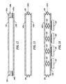
- FIGS. 15 and 16 are plan views of two alternative lid layouts of that may be used in conjunction with the fifth, sixth, seventh and eighth embodiments of the present invention.
- FIGS. 17 is a cross-section view through section 17 — 17 of FIG. 16.
- FIG. 18 is a cross-sectional of a lid with an attached heat sink according to the present invention.
- PCB printed circuit board
- PWB printed wire board
- FIG. 1 is a cross-sectional view of a first embodiment of a multichip module mounted on a PCB having a lid according to the present invention.
- MCM 100 includes a substrate 102 having a multiplicity of components 105 mounted thereto, each component having a front surface 110 and a back surface 115 .
- MCM 100 is mounted to a PCB 120 by a multiplicity of solder balls 125 .
- Substrate 102 may be a single or multi-level substrate and may be ceramic, fiberglass or polymer based.
- MCM 100 also includes a lid 130 . Lid 130 is mounted to substrate 102 by lid support 132 connecting the periphery of lid 130 to the periphery of substrate 102 .
- Lid support 132 may be fabricated from the same material as lid 130 and may be integral with the lid. Alternatively, lid support 132 may be fabricated from a material different from that of lid 130 . Lid support 132 may provide a hermetic seal between lid 130 and substrate 102 .
- Lid 130 includes a lower wall 135 having an outer surface 140 , an upper wall 145 having an outer surface 150 and sidewalls 155 defining a vapor chamber 160 .
- Vapor chamber 160 contains a heat transfer fluid such as, inter alia, water, freon or glycol.
- Front sides 110 of components 105 are electrically connected to a top surface 165 of substrate 102 .
- Components 105 may be flip chip, wire-bonded or soldered to substrate 102 .
- a thermal transfer medium 170 is in contact with back surfaces 115 of components 105 and outer surface 140 of lower wall 135 of lid 130 to enable thermal contact, mechanical restraint and pressure support over the contacting region. Thermal transfer medium 170 enables heat generated by the operation of components 105 to be efficiently transferred to lid 130 .
- lid 130 may be fabricated from many different materials including but not limited to metals such as aluminum, copper, nickel, gold or Invar and other materials such as plastics, ceramics and composites. Because of the wide range of materials available, lid 130 may fabricated from a material having a CTE matched to (between about 25% to 700% of the coefficient of thermal expansion) substrate 102 or from the same material as the substrate. For example, if MCM 100 is a HyperBGATM International Business Machine Corp., Armonk, N.Y., in which substrate 102 is a polytetraflouroethylene (PTFE) based material having a CTE of about 10-12 ppm/° C.
- PTFE polytetraflouroethylene
- lid 130 may be fabricated from an aluminum-silicon carbide composite having a CTE of about 10 ppm/° C.
- lower wall 135 of lid 130 may be fabricated to be thin. For example, if lid 130 were fabricated from copper (CTE about 17 ppm/° C.) and components 105 were fabricated from single-crystal silicon (CTE about 3 ppm/° C.) a thin wall would reduce the stress generated by any mismatch of CTE because the wall could flex.
- lower wall 135 is about 250 microns or less in thickness.
- Thermal transfer medium 170 may be thermal adhesive, thermal grease, thermal-conductive pads, phase change or other materials known in the art.
- MCM 100 has been illustrated in FIG. 1 and described above as a ball grid array (BGA) module, MCM 100 may be pin grid array (PGA) module.
- BGA ball grid array
- PGA pin grid array
- FIG. 2 is a cross-sectional view of a second embodiment of a multichip module mounted on a printed circuit board having a lid according to the present invention.
- lower wall 135 A of lid 130 A has thick protruding regions 180 for maintaining the same or equivalent contact pressure, thermal contact and mechanical restraint on thin components 105 A as is maintained by thin regions 185 on thick components 105 B.
- lid 130 A is identical to lid 130 illustrated in FIG. 1 and described above.
- components having two different thicknesses are illustrated in FIG. 2, the second embodiment of the present invention may be extended to use with components having three of more thicknesses that are different.
- components may be manufactured from semiconductor wafers fabricated from different thickness (i.e 200 and 300 millimeter diameter wafers) or from devices requiring different final thicknesses (i.e. logic, memory and passive devices).
- FIG. 3 is a cross-sectional view of a third embodiment of a multichip module mounted on a printed circuit board having a lid according to the present invention.
- lid 130 B includes a separate lower wall 135 B having an outer surface 140 B and a body 190 having an upper wall 145 having an outer surface 150 and sidewalls 155 defining a vapor chamber 160 .
- Lower wall 135 B is attached to sidewalls 155 by any suitable adhesive 195 , though a resilient adhesive is desirable if the CTE of wall 135 B is significantly different from the CTE of body 190 .
- Lid 130 B and lower wall 135 B may be fabricated from many different materials including but not limited to metals such as aluminum, copper or Invar, plastics, ceramics and composites.
- Body 190 and lower wall 135 B may be fabricated from the same or different materials.
- Body 190 may be fabricated from a material having a coefficient of CTE matched to (between about 25% to 700%) the coefficient of thermal expansion of substrate 120 while lower wall 135 B may be fabricated from a material having a CTE matched to (between about 50% to 700%)the coefficient of thermal expansion of the material of components 105 .
- body 190 may be fabricated from an aluminum-silicon carbide composite (CTE of about 10 ppm/° C.) and lower wall 135 B may be fabricated from glass ceramic (CTE of about 3 ppm/° C.), silicon (CTE of about 3 ppm/° C.) or alumina (CTE of about 6 ppm/° C).
- lower wall 135 B may be fabricated to be thin.
- lower wall 135 B were fabricated from copper (CTE about 17 ppm/° C.) and components 105 were fabricated from single-crystal silicon (CTE about 3 ppm/° C.) a thin wall would reduce the stress generated by the mismatch of CTE because the wall could stretch and flex.
- lower wall 135 B is about 250 microns or less in thickness.
- Lid support 132 may be fabricated from the same or a different material as lid 130 B and may be integral with the lid. Lid support 132 may provide a hermetic seal between lid 130 B and substrate 102 .
- FIG. 4 is a cross-sectional view of a fourth embodiment of a multichip module mounted on a printed circuit board having a lid according to the present invention.
- lower wall 135 C has protruding thick regions 180 for maintaining equivalent contact pressure on thin components 105 A as is maintained by thin regions 185 on thick components 105 B.
- lid 130 C is identical to lid 130 B illustrated in FIG. 3 and described above. While components having two different thicknesses are illustrated in FIG. 4, the fourth embodiment of the present invention may be extended to use with components having three of more thicknesses that are different.
- FIG. 4A provides an alternative cross-section to thick region 180 of lower wall 135 C (see FIG. 4 ). In FIG.
- wall thickness of region 180 A is the same as in thin region 185 (see FIG. 4) but regions 180 A are deflected toward thin components 105 A (by stamping or molding) such that contact is maintained between thermal transfer medium 170 and thin components 105 A while maintaining a thin wall.
- FIG. 5 is a cross-sectional view of a fifth embodiment of a multichip module mounted on a printed circuit board having a lid according to the present invention.
- the fifth embodiment is similar to the first embodiment except that flexural limitations caused in the case of an extremely flexible lower wall 135 are overcome in the fifth embodiment.
- a spreader plate 200 contacting outer surface 150 of lid 130 D secures MCM 100 to PCB 120 via fasteners 205 .
- Fasteners 205 are illustrated in FIG. 5 as screws engaging threaded inserts 210 in PCB 120 , but other suitable fastening means may be used, such as spring clips or rivets.
- supports 215 which, under pressure, contact upper wall 145 and lower wall 135 .
- Supports 215 are aligned over components 105 .
- some or all of supports 215 may be aligned over some or all of components 105 and prevent excessive flexure and buckling of lower wall 135 .
- Supports 215 spread the pressure applied to lid 130 D by spreader plate 200 evenly to each component 105 .
- Land Grid Array (LGA) connections 220 are illustrated between substrate 102 and PCB 120 . Since LGA connections 220 are asperity contact connections, generally some degree of pressure must be maintained on the connection to ensure good electrical conductivity.
- Supports 215 may be fabricated from the same material as lid 130 or a from different material.
- MCM 100 has been illustrated in FIG. 5 and described above as a LGA module, MCM 100 may be BGA or a PGA module.
- FIG. 6 is a cross-sectional view of a sixth embodiment of a multichip module mounted on a printed circuit board having a lid according to the present invention.
- lower wall 135 A of lid 130 E has thick regions 185 for maintaining equivalent contact pressure on thin components 105 A as is maintained by thin regions 180 on thick components 105 B.
- lid 130 E is identical to lid 130 D illustrated in FIG. 5 and described above. While components having two different thicknesses are illustrated in FIG. 6, the second embodiment of the present invention may be extended to use with components having three of more thicknesses that are different.
- FIG. 7 is a cross-sectional view of a seventh embodiment of a multichip module mounted on a printed circuit board having a lid according to the present invention.
- lid 130 G includes a separate lower wall 135 B having an outer surface 140 B and a body 190 having an upper wall 145 having an outer surface 150 and sidewalls 155 defining a vapor chamber 160 .
- Lower wall 135 B is attached to sidewalls 155 by any suitable adhesive 195 , though a resilient adhesive is desirable if the CTE of wall 135 B is significantly different from the CTE of body 190 .
- Lid 130 G and lower wall 135 B may be fabricated from many different materials including but not limited to metals such as aluminum, copper or Invar, plastics, ceramics and composites.
- Body 190 may be fabricated from a material having a coefficient of CTE matched to (between about 25% to 700%) the coefficient of thermal expansion of substrate 102 while lower wall 135 B may be fabricated from a material having a CTE matched to (between about 50% to 700%) the coefficient of thermal expansion of the material of components 105 .
- vapor chamber 160 Within vapor chamber 160 are supports 215 contacting upper wall 145 and lower wall 135 B. Supports 215 are aligned over components 105 . Supports 215 spread the pressure applied to lid 130 G by spreader plate 200 evenly to each component 105 . Lid support 132 and supports 215 may be fabricated from the same material or a different material as body 190 .
- FIG. 8 is a cross-sectional view of an eighth embodiment of a multichip module mounted on a printed circuit board having a lid 130 F according to the present invention.
- lower wall 135 C has thick regions 180 for maintaining equivalent contact pressure on thin components 105 A as is maintained by thin regions 185 on thick components 105 B.
- lid 130 F is identical to lid 130 G illustrated in FIG. 7 and described above. While components having two different thicknesses are illustrated in FIG. 8, the second embodiment of the present invention may be extended to use with components having three of more thicknesses that are different.
- FIG. 8A provides an alternative cross-section to thick region 180 of lower wall 135 C (see FIG. 8 ).
- wall thickness of region 180 A is the same as in thin region 185 (see FIG. 8) but region 180 A is deflected toward thin components 105 A (by stamping or molding) such that contact is maintained to thin components 105 B while maintaining a thin wall.
- FIGS. 9 is a cross-sectional view of an alternative lid construction that may be used in conjunction with the fifth and sixth embodiments of the present invention.
- a lid 130 H includes integral lower wall 135 , integral upper wall 145 and integral sidewalls 155 .
- Integral internal supports 215 join upper wall 145 and lower wall 135 .
- FIGS. 10 and 11 are cross-sectional views of two alternative lid constructions that may be used in conjunction with the seventh and eighth embodiments of the present invention.
- a lid 130 J includes a separate lower wall 135 D and body 190 having an integral upper wall 145 and integral sidewalls 155 .
- Supports 215 are integral with lower wall 135 D and contact upper wall 145 .
- Lower wall 135 D is joined to sidewalls 155 by adhesive 195 .
- a lid 130 K includes a separate lower wall 135 B and a body 190 A having integral upper wall 145 , integral sidewalls 155 and integral supports 215 C. Supports 215 C contact lower wall 135 B.
- Lower wall 135 B is joined to sidewalls 155 by adhesive 195 .
- FIGS. 12 and 13 are cross-sectional views of two alternative lid constructions that may be used in conjunction with the third, fourth, seventh and eighth embodiments of the present invention.
- a lid 130 L includes a separate lower wall 135 F, a body 190 B having an integral upper wall 145 and integral sidewalls 155 A. Lower wall 135 F is joined to sidewalls 155 A by adhesive 195 A.
- a lid 130 M includes a separate lower wall 135 F and a separate upper wall 145 A connected along their respective periphery by a bellows 220 . Internal supports (not shown) as illustrated in FIGS. 10 and 11 and described supra, may be used as well.
- FIG. 14 is a cross-sectional view of a further lid construction that may be used in conjunction with the seventh and eighth embodiments of the present invention.
- a lid 130 N includes separate lower wall 135 F and separate upper wall 145 A connected along their respective periphery by bellows 220 .
- a plurality of internal bellows 225 contact upper wall 145 A and lower wall 135 F. Each internal bellows 225 is aligned over a corresponding component 105 .
- FIGS. 15 and 16 are plan views of two alternative lid layouts of that may be used in conjunction with the fifth, sixth, seventh and eighth embodiments of the present invention.
- lid 130 includes sidewalls 155 enclosing vapor chamber 160 , and a plurality of separate supports 215 . Each support 215 is aligned over a corresponding component 105 .
- lid 130 includes a first pair of opposite facing sidewalls 155 A and 155 B, a second set of opposite facing sidewalls 235 A and 235 B, and a set of elongated supports 215 A ruining between sidewalls 235 A and 235 B.
- the aforementioned sidewalls of lid 130 and supports 215 A enclose each sub-vapor chamber 160 A. Supports 215 A create a set of sub-vapor chambers 160 A. Each support 215 A is aligned over multiple components 105 .
- FIG. 17 is a cross-section view through section 17 - 17 of FIG. 16 .
- support 215 A optionally includes a plurality of holes 240 . Holes 240 interconnect sub-vapor chambers 160 A (see FIG.16) to each other.
- FIG. 18 is a cross-sectional of a lid with an attached heat sink according to the present invention.
- spreader plate 200 (see FIG. 5) is replaced with a heat sink 245 having a plurality of vertical fins 250 .
- Heat sink 245 may be formed from aluminum, copper, beryllium, white metal or any other suitable material with high heat conductivity.
- Heat sink 245 may be fabricated from a material having a CTE matched to (between about 25% to 700%) the CTE of lid 130 D or upper wall 145 in the case of lower wall 135 being a separate piece of lid 130 D as illustrated, for example, in FIG. 7 and described supra. Additionally, lower wall 135 may be fabricated from a material having a CTE matched to (between about 50% to 700%) of the CTE of components 105 in the case of lower wall 135 being a separate piece of lid 130 D.
- the materials of heat sink 245 and lid 130 D may be chosen such that the CTE of the heat sink is matched to (between about 25% to 700%) the CTE of the lid and the CTE of the lid is matched to (between about 50% to 700%) the CTE of components 105 .
Abstract
Description
Claims (18)
Priority Applications (3)
| Application Number | Priority Date | Filing Date | Title |
|---|---|---|---|
| US10/198,393 US6665187B1 (en) | 2002-07-16 | 2002-07-16 | Thermally enhanced lid for multichip modules |
| JP2003181880A JP4346972B2 (en) | 2002-07-16 | 2003-06-25 | Electronic package and heat dissipation method |
| US10/665,669 US7186590B2 (en) | 2002-07-16 | 2003-09-18 | Thermally enhanced lid for multichip modules |
Applications Claiming Priority (1)
| Application Number | Priority Date | Filing Date | Title |
|---|---|---|---|
| US10/198,393 US6665187B1 (en) | 2002-07-16 | 2002-07-16 | Thermally enhanced lid for multichip modules |
Related Child Applications (1)
| Application Number | Title | Priority Date | Filing Date |
|---|---|---|---|
| US10/665,669 Division US7186590B2 (en) | 2002-07-16 | 2003-09-18 | Thermally enhanced lid for multichip modules |
Publications (1)
| Publication Number | Publication Date |
|---|---|
| US6665187B1 true US6665187B1 (en) | 2003-12-16 |
Family
ID=29711460
Family Applications (2)
| Application Number | Title | Priority Date | Filing Date |
|---|---|---|---|
| US10/198,393 Expired - Fee Related US6665187B1 (en) | 2002-07-16 | 2002-07-16 | Thermally enhanced lid for multichip modules |
| US10/665,669 Expired - Fee Related US7186590B2 (en) | 2002-07-16 | 2003-09-18 | Thermally enhanced lid for multichip modules |
Family Applications After (1)
| Application Number | Title | Priority Date | Filing Date |
|---|---|---|---|
| US10/665,669 Expired - Fee Related US7186590B2 (en) | 2002-07-16 | 2003-09-18 | Thermally enhanced lid for multichip modules |
Country Status (2)
| Country | Link |
|---|---|
| US (2) | US6665187B1 (en) |
| JP (1) | JP4346972B2 (en) |
Cited By (59)
| Publication number | Priority date | Publication date | Assignee | Title |
|---|---|---|---|---|
| US20040150102A1 (en) * | 2002-12-30 | 2004-08-05 | Advanced Semiconductor Engineering, Inc. | Thermal enhance MCM package and manufacturing method thereof |
| US20040164388A1 (en) * | 2001-09-01 | 2004-08-26 | Thilo Stolze | Power semiconductor module |
| US6794748B1 (en) * | 2003-04-22 | 2004-09-21 | Intel Corporation | Substrate-less microelectronic package |
| US20050026331A1 (en) * | 2003-07-31 | 2005-02-03 | Tz-Cheng Chiu | Composite lid for land grid array (lga) flip-chip package assembly |
| US20050068736A1 (en) * | 2003-09-26 | 2005-03-31 | Tokyo Electron Limited | Method and apparatus for efficient temperature control using a contact volume |
| US20050088822A1 (en) * | 2003-10-27 | 2005-04-28 | Oberlin Gary E. | Power electronic system with passive cooling |
| US20050274487A1 (en) * | 2004-05-27 | 2005-12-15 | International Business Machines Corporation | Method and apparatus for reducing thermal resistance in a vertical heat sink assembly |
| US20060039118A1 (en) * | 2004-08-19 | 2006-02-23 | Behdad Jafari | Method and apparatus for heat dissipation |
| US20060050483A1 (en) * | 2004-09-08 | 2006-03-09 | Wilson Michael J | Liquid cooled heat sink with cold plate retention mechanism |
| US20060096740A1 (en) * | 2004-11-10 | 2006-05-11 | Wen-Chun Zheng | Nearly isothermal heat pipe heat sink and process for making the same |
| US20060146503A1 (en) * | 2003-04-16 | 2006-07-06 | Fujitsu Limited | Electronic component package including heat spreading member |
| US20070139892A1 (en) * | 2005-12-20 | 2007-06-21 | Fujitsu Limited | Semiconductor device |
| US20070156938A1 (en) * | 2005-12-28 | 2007-07-05 | Manbo Wu | Interconnect structure between HyperTransport bus interface boards |
| US20080266786A1 (en) * | 2007-04-25 | 2008-10-30 | Behdad Jafari | Method and apparatus for heat dissipation |
| US20090021918A1 (en) * | 2006-08-31 | 2009-01-22 | Adlink Technology Inc. | Stacked heat-transfer interface structure |
| US20090129022A1 (en) * | 2002-01-11 | 2009-05-21 | Intel Corporation | Micro-chimney and thermosiphon die-level cooling |
| US20090219698A1 (en) * | 2006-12-05 | 2009-09-03 | Tong Wa Chao | Heat Spreader for a multi-chip package |
| US20090294955A1 (en) * | 2007-07-23 | 2009-12-03 | International Business Machines Corporation | Cooling device with a preformed compliant interface |
| US20100044015A1 (en) * | 2006-11-13 | 2010-02-25 | Aavid Thermalloy, Llc | Heat Sink |
| US20100246128A1 (en) * | 2009-03-31 | 2010-09-30 | Domhnaill Hernon | Circuit Pack Cooling Solution |
| US20100294461A1 (en) * | 2009-05-22 | 2010-11-25 | General Electric Company | Enclosure for heat transfer devices, methods of manufacture thereof and articles comprising the same |
| US7864532B1 (en) * | 2004-10-18 | 2011-01-04 | Lockheed Martin Corporation | Molded or encapsulated transmit-receive module or TR module/antenna element for active array |
| US20110024892A1 (en) * | 2009-07-30 | 2011-02-03 | Taiwan Semiconductor Manufacturing Company, Ltd. | Thermally enhanced heat spreader for flip chip packaging |
| CN102149266A (en) * | 2010-02-04 | 2011-08-10 | 台烨科技股份有限公司 | Temperature equalizing plate |
| US20110247785A1 (en) * | 2008-12-29 | 2011-10-13 | Hewlett-Packard Development Company, L.P. | Systems and Method of a Carrier Device for Placement of Thermal Interface Materials |
| US20120098118A1 (en) * | 2010-10-20 | 2012-04-26 | Taiwan Semiconductor Manufacturing Company, Ltd. | Compliant heat spreader for flip chip packaging |
| CN102595861A (en) * | 2012-03-12 | 2012-07-18 | 华南理工大学 | Vapor chamber having support posts with inner-sintering structure |
| US20120243166A1 (en) * | 2011-03-21 | 2012-09-27 | Eldon Technology Limited | Media content device chassis with internal extension members |
| US20120250260A1 (en) * | 2011-03-29 | 2012-10-04 | Eldon Technology Limited | Media content device with customized panel |
| US8363411B2 (en) | 2011-03-18 | 2013-01-29 | Eldon Technology Limited | Passive, low-profile heat transferring system |
| US8638199B2 (en) | 2011-03-29 | 2014-01-28 | Eldon Technology Limited | Apparatus, systems and methods for power line carrier data communication to DC powered electronic device |
| US8682169B2 (en) | 2011-02-28 | 2014-03-25 | Eldon Technology Limited | Apparatus, systems and methods for detecting infrared signals at a media device configured to be positioned in different orientations |
| US8681495B2 (en) | 2011-03-29 | 2014-03-25 | Eldon Technology Limited | Media device having a piezoelectric fan |
| US20140084439A1 (en) * | 2012-09-21 | 2014-03-27 | Fujitsu Semiconductor Limited | Semiconductor device, electronic device and method for fabricating the semiconductor device |
| US20140110859A1 (en) * | 2012-10-09 | 2014-04-24 | Mc10, Inc. | Embedding thin chips in polymer |
| US20140153191A1 (en) * | 2012-12-04 | 2014-06-05 | Hamilton Sundstrand Corporation | Electronic Component Cooling Hood and Heat Pipe |
| US20140167244A1 (en) * | 2012-12-17 | 2014-06-19 | Princo Middle East Fze | Chip thermal dissipation structure |
| US20140167216A1 (en) * | 2012-12-13 | 2014-06-19 | Nvidia Corporation | Low-profile chip package with modified heat spreader |
| US20140217870A1 (en) * | 2013-02-01 | 2014-08-07 | Emerson Network Power - Embedded Computing, Inc. | Method and device to provide uniform cooling in rugged environments |
| DE102008034033B4 (en) * | 2008-07-22 | 2014-11-27 | Ust Umweltsensortechnik Gmbh | Microelectronic sensor component |
| US20140355301A1 (en) * | 2013-05-31 | 2014-12-04 | Samsung Display Co., Ltd. | Display device |
| US20150076676A1 (en) * | 2013-09-17 | 2015-03-19 | Jun Lu | Power semiconductor device package and fabrication method |
| US9047492B2 (en) | 2011-03-22 | 2015-06-02 | Echostar Uk Holdings Limited | Apparatus, systems and methods for securely storing media content events on a flash memory device |
| US20150170989A1 (en) * | 2013-12-16 | 2015-06-18 | Hemanth K. Dhavaleswarapu | Three-dimensional (3d) integrated heat spreader for multichip packages |
| US20160035637A1 (en) * | 2014-08-01 | 2016-02-04 | Socionext Inc. | Semiconductor device and manufacturing method of semiconductor device |
| CN106546116A (en) * | 2015-09-23 | 2017-03-29 | 迈萪科技股份有限公司 | Temperature equalizing plate and manufacturing method thereof |
| US9721868B2 (en) | 2009-07-30 | 2017-08-01 | Taiwan Semiconductor Manufacturing Company, Ltd. | Three dimensional integrated circuit (3DIC) having a thermally enhanced heat spreader embedded in a substrate |
| US20170229374A1 (en) * | 2016-02-10 | 2017-08-10 | International Business Machines Corporation | Heat sink with integrated threaded lid |
| US20180076113A1 (en) * | 2016-09-15 | 2018-03-15 | International Business Machines Corporation | Chip package for two-phase cooling and assembly process thereof |
| US20180096913A1 (en) * | 2016-10-05 | 2018-04-05 | Jaehong Park | Semiconductor Packages |
| US20190035713A1 (en) * | 2017-07-28 | 2019-01-31 | Qualcomm Incorporated | Systems and methods for cooling an electronic device |
| US10381287B1 (en) * | 2018-01-31 | 2019-08-13 | Mentor Graphics Corporation | Heat sink interface for a device |
| US20210329809A1 (en) * | 2018-10-17 | 2021-10-21 | Delta Electronics, Inc. | Power module having metallic heat-dissipation substrate |
| US11557521B2 (en) | 2017-10-26 | 2023-01-17 | Mitsubishi Electric Corporation | Heat sink and circuit device |
| EP4216269A1 (en) * | 2022-01-25 | 2023-07-26 | GE Aviation Systems LLC | Power overlay module with thermal storage |
| US11769710B2 (en) * | 2020-03-27 | 2023-09-26 | Xilinx, Inc. | Heterogeneous integration module comprising thermal management apparatus |
| US20230345613A1 (en) * | 2022-04-25 | 2023-10-26 | Nvidia Corporation | Printed circuit board assembly with integrated vapor chamber |
| US11882645B2 (en) | 2021-10-22 | 2024-01-23 | International Business Machines Corporation | Multi chip hardware security module |
| US11948855B1 (en) | 2019-09-27 | 2024-04-02 | Rockwell Collins, Inc. | Integrated circuit (IC) package with cantilever multi-chip module (MCM) heat spreader |
Families Citing this family (24)
| Publication number | Priority date | Publication date | Assignee | Title |
|---|---|---|---|---|
| US20040011509A1 (en) * | 2002-05-15 | 2004-01-22 | Wing Ming Siu | Vapor augmented heatsink with multi-wick structure |
| US20070164424A1 (en) * | 2003-04-02 | 2007-07-19 | Nancy Dean | Thermal interconnect and interface systems, methods of production and uses thereof |
| WO2004109795A2 (en) * | 2003-06-06 | 2004-12-16 | Honeywell International Inc. | Thermal interconnect system and method of production thereof |
| US20090027857A1 (en) * | 2004-03-30 | 2009-01-29 | Dean Nancy F | Heat spreader constructions, intergrated circuitry, methods of forming heat spreader constructions, and methods of forming integrated circuitry |
| TWI311363B (en) * | 2005-04-22 | 2009-06-21 | Foxconn Tech Co Ltd | Boiling chamber cooling device |
| KR101519601B1 (en) * | 2008-09-09 | 2015-05-13 | 삼성전자주식회사 | A Semiconductor Module And An Electronic System Including The Same |
| US8422229B2 (en) * | 2009-06-25 | 2013-04-16 | Oracle America, Inc. | Molded heat sink and method of making same |
| DE102010042168A1 (en) * | 2010-10-07 | 2012-04-12 | Robert Bosch Gmbh | Electronic assembly and method for its production |
| US9153520B2 (en) | 2011-11-14 | 2015-10-06 | Micron Technology, Inc. | Stacked semiconductor die assemblies with multiple thermal paths and associated systems and methods |
| US9036353B2 (en) * | 2012-11-26 | 2015-05-19 | Northrop Grumman Systems Corporation | Flexible thermal interface for electronics |
| US9287194B2 (en) * | 2013-03-06 | 2016-03-15 | Taiwan Semiconductor Manufacturing Company, Ltd. | Packaging devices and methods for semiconductor devices |
| US10276957B2 (en) * | 2013-08-27 | 2019-04-30 | Continental Automotive Systems, Inc. | Grounding method for baseplate sealed enclosures |
| US20150173243A1 (en) * | 2013-12-13 | 2015-06-18 | General Electric Company | Integrated heat exchange assembly and an associated method thereof |
| US9490188B2 (en) | 2014-09-12 | 2016-11-08 | International Business Machines Corporation | Compute intensive module packaging |
| US9823718B2 (en) | 2016-01-13 | 2017-11-21 | Microsoft Technology Licensing, Llc | Device cooling |
| CN108323137A (en) * | 2017-01-18 | 2018-07-24 | 台达电子工业股份有限公司 | Soaking plate |
| JP6905678B2 (en) * | 2017-03-27 | 2021-07-21 | 大日本印刷株式会社 | Vapor chamber, substrate for vapor chamber and metal sheet for vapor chamber |
| US10147664B2 (en) | 2017-04-24 | 2018-12-04 | Xilinx, Inc. | Dynamic mounting thermal management for devices on board |
| KR102439761B1 (en) | 2017-12-22 | 2022-09-02 | 삼성전자주식회사 | Electronic device and method of manufacturing an electronic device |
| US20190387615A1 (en) * | 2018-06-14 | 2019-12-19 | Microsoft Technology Licensing, Llc | Multi-layer interconnected electro-thermal system having a thermally non-expansive support for mounting positionally related sensor components |
| US11894286B2 (en) * | 2019-06-13 | 2024-02-06 | Bae Systems Information And Electronic Systems Integration Inc. | Hermetically sealed electronics module with enhanced cooling of core integrated circuit |
| US11699681B2 (en) * | 2019-12-26 | 2023-07-11 | Intel Corporation | Multi-chip module having a stacked logic chip and memory stack |
| US11239134B2 (en) * | 2020-01-17 | 2022-02-01 | Taiwan Semiconductor Manufacturing Company, Ltd. | Package structure and method of fabricating the same |
| US11804468B2 (en) | 2021-01-15 | 2023-10-31 | Taiwan Semiconductor Manufacturing Company, Ltd. | Manufacturing method of semiconductor package using jig |
Citations (12)
| Publication number | Priority date | Publication date | Assignee | Title |
|---|---|---|---|---|
| US4612978A (en) * | 1983-07-14 | 1986-09-23 | Cutchaw John M | Apparatus for cooling high-density integrated circuit packages |
| US5179500A (en) | 1990-02-27 | 1993-01-12 | Grumman Aerospace Corporation | Vapor chamber cooled electronic circuit card |
| US5216580A (en) | 1992-01-14 | 1993-06-01 | Sun Microsystems, Inc. | Optimized integral heat pipe and electronic circuit module arrangement |
| US5325265A (en) * | 1988-11-10 | 1994-06-28 | Mcnc | High performance integrated circuit chip package |
| US5704416A (en) * | 1993-09-10 | 1998-01-06 | Aavid Laboratories, Inc. | Two phase component cooler |
| US5880524A (en) * | 1997-05-05 | 1999-03-09 | Intel Corporation | Heat pipe lid for electronic packages |
| US5915463A (en) | 1996-03-23 | 1999-06-29 | Motorola, Inc. | Heat dissipation apparatus and method |
| US6085831A (en) | 1999-03-03 | 2000-07-11 | International Business Machines Corporation | Direct chip-cooling through liquid vaporization heat exchange |
| US6091603A (en) | 1999-09-30 | 2000-07-18 | International Business Machines Corporation | Customizable lid for improved thermal performance of modules using flip chips |
| US6166908A (en) | 1999-10-01 | 2000-12-26 | Intel Corporation | Integrated circuit cartridge |
| US6212074B1 (en) | 2000-01-31 | 2001-04-03 | Sun Microsystems, Inc. | Apparatus for dissipating heat from a circuit board having a multilevel surface |
| US6429513B1 (en) * | 2001-05-25 | 2002-08-06 | Amkor Technology, Inc. | Active heat sink for cooling a semiconductor chip |
Family Cites Families (27)
| Publication number | Priority date | Publication date | Assignee | Title |
|---|---|---|---|---|
| US3957107A (en) * | 1975-02-27 | 1976-05-18 | The United States Of America As Represented By The Secretary Of The Air Force | Thermal switch |
| US4313492A (en) * | 1979-12-20 | 1982-02-02 | International Business Machines Corporation | Micro helix thermo capsule |
| JPS60214942A (en) * | 1984-04-10 | 1985-10-28 | 株式会社 潤工社 | Oriented porous ethylene tetrafluoride resin body difficult to be deformed by compression |
| US4996589A (en) * | 1987-10-21 | 1991-02-26 | Hitachi, Ltd. | Semiconductor module and cooling device of the same |
| US5097387A (en) * | 1990-06-27 | 1992-03-17 | Digital Equipment Corporation | Circuit chip package employing low melting point solder for heat transfer |
| DE4121534C2 (en) * | 1990-06-30 | 1998-10-08 | Toshiba Kawasaki Kk | Cooler |
| JP3288840B2 (en) * | 1994-02-28 | 2002-06-04 | 三菱電機株式会社 | Semiconductor device and manufacturing method thereof |
| US6269866B1 (en) * | 1997-02-13 | 2001-08-07 | The Furukawa Electric Co., Ltd. | Cooling device with heat pipe |
| US6133631A (en) * | 1997-05-30 | 2000-10-17 | Hewlett-Packard Company | Semiconductor package lid with internal heat pipe |
| US5933323A (en) * | 1997-11-05 | 1999-08-03 | Intel Corporation | Electronic component lid that provides improved thermal dissipation |
| JP2000273196A (en) * | 1999-03-24 | 2000-10-03 | Polymatech Co Ltd | Heat-conductive resin substrate and semiconductor package |
| US6329603B1 (en) * | 1999-04-07 | 2001-12-11 | International Business Machines Corporation | Low CTE power and ground planes |
| US6490160B2 (en) * | 1999-07-15 | 2002-12-03 | Incep Technologies, Inc. | Vapor chamber with integrated pin array |
| US6556455B2 (en) * | 1999-07-15 | 2003-04-29 | Incep Technologies, Inc. | Ultra-low impedance power interconnection system for electronic packages |
| US6410982B1 (en) * | 1999-11-12 | 2002-06-25 | Intel Corporation | Heatpipesink having integrated heat pipe and heat sink |
| US6550531B1 (en) * | 2000-05-16 | 2003-04-22 | Intel Corporation | Vapor chamber active heat sink |
| US6313994B1 (en) * | 2000-07-25 | 2001-11-06 | Sun Microsystems, Inc. | Extended surface area heat sink |
| US6292369B1 (en) * | 2000-08-07 | 2001-09-18 | International Business Machines Corporation | Methods for customizing lid for improved thermal performance of modules using flip chips |
| US6639799B2 (en) * | 2000-12-22 | 2003-10-28 | Intel Corporation | Integrated vapor chamber heat sink and spreader and an embedded direct heat pipe attachment |
| US20020144804A1 (en) * | 2001-01-19 | 2002-10-10 | Yue Liang | Thermal transfer device and working fluid therefor including a kinetic ice inhibitor |
| US20030024698A1 (en) * | 2001-08-01 | 2003-02-06 | International Business Machines Corporation | Flexible coupling for heat sink |
| US6590409B1 (en) * | 2001-12-13 | 2003-07-08 | Lsi Logic Corporation | Systems and methods for package defect detection |
| US7036573B2 (en) * | 2002-02-08 | 2006-05-02 | Intel Corporation | Polymer with solder pre-coated fillers for thermal interface materials |
| US20030155102A1 (en) * | 2002-02-15 | 2003-08-21 | Garner Scott D. | Vapor chamber having integral captive fasteners |
| US6637506B2 (en) * | 2002-03-08 | 2003-10-28 | Sun Microsystems, Inc. | Multi-material heat spreader |
| US6727193B2 (en) * | 2002-03-08 | 2004-04-27 | Sun Microsystems, Inc. | Apparatus and methods for enhancing thermal performance of integrated circuit packages |
| US6717246B2 (en) * | 2002-04-16 | 2004-04-06 | Intel Corporation | Semiconductor package with integrated conical vapor chamber |
-
2002
- 2002-07-16 US US10/198,393 patent/US6665187B1/en not_active Expired - Fee Related
-
2003
- 2003-06-25 JP JP2003181880A patent/JP4346972B2/en not_active Expired - Fee Related
- 2003-09-18 US US10/665,669 patent/US7186590B2/en not_active Expired - Fee Related
Patent Citations (12)
| Publication number | Priority date | Publication date | Assignee | Title |
|---|---|---|---|---|
| US4612978A (en) * | 1983-07-14 | 1986-09-23 | Cutchaw John M | Apparatus for cooling high-density integrated circuit packages |
| US5325265A (en) * | 1988-11-10 | 1994-06-28 | Mcnc | High performance integrated circuit chip package |
| US5179500A (en) | 1990-02-27 | 1993-01-12 | Grumman Aerospace Corporation | Vapor chamber cooled electronic circuit card |
| US5216580A (en) | 1992-01-14 | 1993-06-01 | Sun Microsystems, Inc. | Optimized integral heat pipe and electronic circuit module arrangement |
| US5704416A (en) * | 1993-09-10 | 1998-01-06 | Aavid Laboratories, Inc. | Two phase component cooler |
| US5915463A (en) | 1996-03-23 | 1999-06-29 | Motorola, Inc. | Heat dissipation apparatus and method |
| US5880524A (en) * | 1997-05-05 | 1999-03-09 | Intel Corporation | Heat pipe lid for electronic packages |
| US6085831A (en) | 1999-03-03 | 2000-07-11 | International Business Machines Corporation | Direct chip-cooling through liquid vaporization heat exchange |
| US6091603A (en) | 1999-09-30 | 2000-07-18 | International Business Machines Corporation | Customizable lid for improved thermal performance of modules using flip chips |
| US6166908A (en) | 1999-10-01 | 2000-12-26 | Intel Corporation | Integrated circuit cartridge |
| US6212074B1 (en) | 2000-01-31 | 2001-04-03 | Sun Microsystems, Inc. | Apparatus for dissipating heat from a circuit board having a multilevel surface |
| US6429513B1 (en) * | 2001-05-25 | 2002-08-06 | Amkor Technology, Inc. | Active heat sink for cooling a semiconductor chip |
Cited By (104)
| Publication number | Priority date | Publication date | Assignee | Title |
|---|---|---|---|---|
| US20040164388A1 (en) * | 2001-09-01 | 2004-08-26 | Thilo Stolze | Power semiconductor module |
| US8227913B2 (en) * | 2001-09-01 | 2012-07-24 | Infineon Technologies Ag | Power semiconductor module comprising elastic housing for accommodating movement of individual substrate regions on a heat sink |
| US8505613B2 (en) * | 2002-01-11 | 2013-08-13 | Intel Corporation | Die having a via filled with a heat-dissipating material |
| US20090129022A1 (en) * | 2002-01-11 | 2009-05-21 | Intel Corporation | Micro-chimney and thermosiphon die-level cooling |
| US8006747B2 (en) * | 2002-01-11 | 2011-08-30 | Intel Corporation | Micro-chimney and thermosiphon die-level cooling |
| US20110297362A1 (en) * | 2002-01-11 | 2011-12-08 | Chrysler Gregory M | Micro-chimney and thermosiphon die-level cooling |
| US20040150102A1 (en) * | 2002-12-30 | 2004-08-05 | Advanced Semiconductor Engineering, Inc. | Thermal enhance MCM package and manufacturing method thereof |
| US7002805B2 (en) * | 2002-12-30 | 2006-02-21 | Advanced Semiconductor Engineering Inc. | Thermal enhance MCM package and manufacturing method thereof |
| US20060146503A1 (en) * | 2003-04-16 | 2006-07-06 | Fujitsu Limited | Electronic component package including heat spreading member |
| US7477519B2 (en) * | 2003-04-16 | 2009-01-13 | Fujitsu Limited | Electronic component package including heat spreading member |
| US6965163B2 (en) | 2003-04-22 | 2005-11-15 | Intel Corporation | Substrate-less microelectronic package |
| US20050006787A1 (en) * | 2003-04-22 | 2005-01-13 | Chia-Pin Chiu | Substrate-less microelectronic package |
| US6794748B1 (en) * | 2003-04-22 | 2004-09-21 | Intel Corporation | Substrate-less microelectronic package |
| US6861292B2 (en) * | 2003-07-31 | 2005-03-01 | Texas Instruments Incorporated | Composite lid for land grid array (LGA) flip-chip package assembly |
| US20050026331A1 (en) * | 2003-07-31 | 2005-02-03 | Tz-Cheng Chiu | Composite lid for land grid array (lga) flip-chip package assembly |
| US6992892B2 (en) * | 2003-09-26 | 2006-01-31 | Tokyo Electron Limited | Method and apparatus for efficient temperature control using a contact volume |
| US20050068736A1 (en) * | 2003-09-26 | 2005-03-31 | Tokyo Electron Limited | Method and apparatus for efficient temperature control using a contact volume |
| US7106588B2 (en) * | 2003-10-27 | 2006-09-12 | Delphi Technologies, Inc. | Power electronic system with passive cooling |
| US20050088822A1 (en) * | 2003-10-27 | 2005-04-28 | Oberlin Gary E. | Power electronic system with passive cooling |
| US20050274487A1 (en) * | 2004-05-27 | 2005-12-15 | International Business Machines Corporation | Method and apparatus for reducing thermal resistance in a vertical heat sink assembly |
| US20060039118A1 (en) * | 2004-08-19 | 2006-02-23 | Behdad Jafari | Method and apparatus for heat dissipation |
| US7254033B2 (en) * | 2004-08-19 | 2007-08-07 | Behdad Jafari | Method and apparatus for heat dissipation |
| US20060050483A1 (en) * | 2004-09-08 | 2006-03-09 | Wilson Michael J | Liquid cooled heat sink with cold plate retention mechanism |
| US7149087B2 (en) * | 2004-09-08 | 2006-12-12 | Thermal Corp. | Liquid cooled heat sink with cold plate retention mechanism |
| US7864532B1 (en) * | 2004-10-18 | 2011-01-04 | Lockheed Martin Corporation | Molded or encapsulated transmit-receive module or TR module/antenna element for active array |
| US7677299B2 (en) | 2004-11-10 | 2010-03-16 | Wen-Chun Zheng | Nearly isothermal heat pipe heat sink |
| US20060096740A1 (en) * | 2004-11-10 | 2006-05-11 | Wen-Chun Zheng | Nearly isothermal heat pipe heat sink and process for making the same |
| US7813133B2 (en) * | 2005-12-20 | 2010-10-12 | Fujitsu Semiconductor Limited | Semiconductor device |
| US20070139892A1 (en) * | 2005-12-20 | 2007-06-21 | Fujitsu Limited | Semiconductor device |
| US20070156938A1 (en) * | 2005-12-28 | 2007-07-05 | Manbo Wu | Interconnect structure between HyperTransport bus interface boards |
| WO2007073647A1 (en) * | 2005-12-28 | 2007-07-05 | Huawei Technologies Co., Ltd. | Interconnect structure between hyper-transport bus interface boards |
| US7684198B2 (en) * | 2006-08-31 | 2010-03-23 | Adlink Technology Inc. | Stacked heat-transfer interface structure |
| US20090021918A1 (en) * | 2006-08-31 | 2009-01-22 | Adlink Technology Inc. | Stacked heat-transfer interface structure |
| US20100044015A1 (en) * | 2006-11-13 | 2010-02-25 | Aavid Thermalloy, Llc | Heat Sink |
| US8616267B2 (en) * | 2006-11-13 | 2013-12-31 | Aavid Thermalloy, Llc | Heat sink |
| US20090219698A1 (en) * | 2006-12-05 | 2009-09-03 | Tong Wa Chao | Heat Spreader for a multi-chip package |
| US7944046B2 (en) * | 2006-12-05 | 2011-05-17 | Intel Corporation | Heat spreader for a multi-chip package |
| US20080266786A1 (en) * | 2007-04-25 | 2008-10-30 | Behdad Jafari | Method and apparatus for heat dissipation |
| US20090294955A1 (en) * | 2007-07-23 | 2009-12-03 | International Business Machines Corporation | Cooling device with a preformed compliant interface |
| DE102008034033B4 (en) * | 2008-07-22 | 2014-11-27 | Ust Umweltsensortechnik Gmbh | Microelectronic sensor component |
| US20110247785A1 (en) * | 2008-12-29 | 2011-10-13 | Hewlett-Packard Development Company, L.P. | Systems and Method of a Carrier Device for Placement of Thermal Interface Materials |
| US8576566B2 (en) * | 2008-12-29 | 2013-11-05 | Hewlett-Packard Development Company, L.P. | Systems and method of a carrier device for placement of thermal interface materials |
| US7929306B2 (en) * | 2009-03-31 | 2011-04-19 | Alcatel-Lucent Usa Inc. | Circuit pack cooling solution |
| US20100246128A1 (en) * | 2009-03-31 | 2010-09-30 | Domhnaill Hernon | Circuit Pack Cooling Solution |
| US20100294461A1 (en) * | 2009-05-22 | 2010-11-25 | General Electric Company | Enclosure for heat transfer devices, methods of manufacture thereof and articles comprising the same |
| US20110024892A1 (en) * | 2009-07-30 | 2011-02-03 | Taiwan Semiconductor Manufacturing Company, Ltd. | Thermally enhanced heat spreader for flip chip packaging |
| US8970029B2 (en) * | 2009-07-30 | 2015-03-03 | Taiwan Semiconductor Manufacturing Company, Ltd. | Thermally enhanced heat spreader for flip chip packaging |
| US9721868B2 (en) | 2009-07-30 | 2017-08-01 | Taiwan Semiconductor Manufacturing Company, Ltd. | Three dimensional integrated circuit (3DIC) having a thermally enhanced heat spreader embedded in a substrate |
| CN102149266A (en) * | 2010-02-04 | 2011-08-10 | 台烨科技股份有限公司 | Temperature equalizing plate |
| US8779582B2 (en) * | 2010-10-20 | 2014-07-15 | Taiwan Semiconductor Manufacturing Company, Ltd. | Compliant heat spreader for flip chip packaging having thermally-conductive element with different metal material areas |
| US20120098118A1 (en) * | 2010-10-20 | 2012-04-26 | Taiwan Semiconductor Manufacturing Company, Ltd. | Compliant heat spreader for flip chip packaging |
| US8682169B2 (en) | 2011-02-28 | 2014-03-25 | Eldon Technology Limited | Apparatus, systems and methods for detecting infrared signals at a media device configured to be positioned in different orientations |
| US8363411B2 (en) | 2011-03-18 | 2013-01-29 | Eldon Technology Limited | Passive, low-profile heat transferring system |
| US8953324B2 (en) | 2011-03-21 | 2015-02-10 | Eldon Technology Limited | Media content device chassis with internal extension members |
| US8619427B2 (en) * | 2011-03-21 | 2013-12-31 | Eldon Technology Limited | Media content device chassis with internal extension members |
| US20120243166A1 (en) * | 2011-03-21 | 2012-09-27 | Eldon Technology Limited | Media content device chassis with internal extension members |
| US9047492B2 (en) | 2011-03-22 | 2015-06-02 | Echostar Uk Holdings Limited | Apparatus, systems and methods for securely storing media content events on a flash memory device |
| US9218300B2 (en) | 2011-03-22 | 2015-12-22 | Echostar Uk Holdings Limited | Apparatus, systems and methods for securely storing media content events on a flash memory device |
| US9319103B2 (en) | 2011-03-29 | 2016-04-19 | Echostar Uk Holdings Limited | Apparatus, systems and methods for power line carrier data communication to DC powered electronic device |
| US9317079B2 (en) * | 2011-03-29 | 2016-04-19 | Echostar Uk Holdings Limited | Media content device with customized panel |
| US8638199B2 (en) | 2011-03-29 | 2014-01-28 | Eldon Technology Limited | Apparatus, systems and methods for power line carrier data communication to DC powered electronic device |
| US8830040B2 (en) | 2011-03-29 | 2014-09-09 | Eldon Technology Limited | Apparatus, systems and methods for power line carrier data communication to DC powered electronic device |
| US20120250260A1 (en) * | 2011-03-29 | 2012-10-04 | Eldon Technology Limited | Media content device with customized panel |
| US8681495B2 (en) | 2011-03-29 | 2014-03-25 | Eldon Technology Limited | Media device having a piezoelectric fan |
| CN102595861A (en) * | 2012-03-12 | 2012-07-18 | 华南理工大学 | Vapor chamber having support posts with inner-sintering structure |
| CN102595861B (en) * | 2012-03-12 | 2014-12-31 | 华南理工大学 | Vapor chamber having support posts with inner-sintering structure |
| US9385092B2 (en) * | 2012-09-21 | 2016-07-05 | Socionext Inc. | Semiconductor device, electronic device and method for fabricating the semiconductor device |
| US20140084439A1 (en) * | 2012-09-21 | 2014-03-27 | Fujitsu Semiconductor Limited | Semiconductor device, electronic device and method for fabricating the semiconductor device |
| US9583428B2 (en) | 2012-10-09 | 2017-02-28 | Mc10, Inc. | Embedding thin chips in polymer |
| US20140110859A1 (en) * | 2012-10-09 | 2014-04-24 | Mc10, Inc. | Embedding thin chips in polymer |
| US9171794B2 (en) * | 2012-10-09 | 2015-10-27 | Mc10, Inc. | Embedding thin chips in polymer |
| US9013879B2 (en) * | 2012-12-04 | 2015-04-21 | Hamilton Sundstrand Corporation | Electronic component cooling hood and heat pipe |
| US20140153191A1 (en) * | 2012-12-04 | 2014-06-05 | Hamilton Sundstrand Corporation | Electronic Component Cooling Hood and Heat Pipe |
| US9530714B2 (en) * | 2012-12-13 | 2016-12-27 | Nvidia Corporation | Low-profile chip package with modified heat spreader |
| US20140167216A1 (en) * | 2012-12-13 | 2014-06-19 | Nvidia Corporation | Low-profile chip package with modified heat spreader |
| US20140167244A1 (en) * | 2012-12-17 | 2014-06-19 | Princo Middle East Fze | Chip thermal dissipation structure |
| US9117792B2 (en) * | 2012-12-17 | 2015-08-25 | Princo Middle East Fze | Chip thermal dissipation structure |
| US11006548B2 (en) * | 2013-02-01 | 2021-05-11 | Smart Embedded Computing, Inc. | Method and device to provide uniform cooling in rugged environments |
| US20140217870A1 (en) * | 2013-02-01 | 2014-08-07 | Emerson Network Power - Embedded Computing, Inc. | Method and device to provide uniform cooling in rugged environments |
| US20140355301A1 (en) * | 2013-05-31 | 2014-12-04 | Samsung Display Co., Ltd. | Display device |
| US9354383B2 (en) * | 2013-05-31 | 2016-05-31 | Samsung Display Co., Ltd. | Display device including an adhesive member |
| US20150076676A1 (en) * | 2013-09-17 | 2015-03-19 | Jun Lu | Power semiconductor device package and fabrication method |
| US20150170989A1 (en) * | 2013-12-16 | 2015-06-18 | Hemanth K. Dhavaleswarapu | Three-dimensional (3d) integrated heat spreader for multichip packages |
| US9716049B2 (en) * | 2014-08-01 | 2017-07-25 | Socionext Inc. | Semiconductor device and manufacturing method of semiconductor device |
| US20160035637A1 (en) * | 2014-08-01 | 2016-02-04 | Socionext Inc. | Semiconductor device and manufacturing method of semiconductor device |
| CN106546116A (en) * | 2015-09-23 | 2017-03-29 | 迈萪科技股份有限公司 | Temperature equalizing plate and manufacturing method thereof |
| US20170229374A1 (en) * | 2016-02-10 | 2017-08-10 | International Business Machines Corporation | Heat sink with integrated threaded lid |
| US10002819B2 (en) * | 2016-02-10 | 2018-06-19 | International Business Machines Corporation | Heat sink with integrated threaded lid |
| US10607963B2 (en) * | 2016-09-15 | 2020-03-31 | International Business Machines Corporation | Chip package for two-phase cooling and assembly process thereof |
| US20180076113A1 (en) * | 2016-09-15 | 2018-03-15 | International Business Machines Corporation | Chip package for two-phase cooling and assembly process thereof |
| US10177072B2 (en) * | 2016-10-05 | 2019-01-08 | Samsung Electronics Co., Ltd. | Semiconductor packages that include a heat pipe for exhausting heat from one or more ends of the package |
| US20180096913A1 (en) * | 2016-10-05 | 2018-04-05 | Jaehong Park | Semiconductor Packages |
| US10446471B2 (en) | 2016-10-05 | 2019-10-15 | Samsung Electronics Co., Ltd. | Semiconductor packages that include a heat pipe for exhausting heat from one or more ends of the package |
| US20190035713A1 (en) * | 2017-07-28 | 2019-01-31 | Qualcomm Incorporated | Systems and methods for cooling an electronic device |
| US10622282B2 (en) * | 2017-07-28 | 2020-04-14 | Qualcomm Incorporated | Systems and methods for cooling an electronic device |
| US11557521B2 (en) | 2017-10-26 | 2023-01-17 | Mitsubishi Electric Corporation | Heat sink and circuit device |
| US10381287B1 (en) * | 2018-01-31 | 2019-08-13 | Mentor Graphics Corporation | Heat sink interface for a device |
| US20210329809A1 (en) * | 2018-10-17 | 2021-10-21 | Delta Electronics, Inc. | Power module having metallic heat-dissipation substrate |
| US11622475B2 (en) * | 2018-10-17 | 2023-04-04 | Delta Electronics, Inc. | Power module having metallic heat-dissipation substrate |
| US11948855B1 (en) | 2019-09-27 | 2024-04-02 | Rockwell Collins, Inc. | Integrated circuit (IC) package with cantilever multi-chip module (MCM) heat spreader |
| US11769710B2 (en) * | 2020-03-27 | 2023-09-26 | Xilinx, Inc. | Heterogeneous integration module comprising thermal management apparatus |
| US11882645B2 (en) | 2021-10-22 | 2024-01-23 | International Business Machines Corporation | Multi chip hardware security module |
| EP4216269A1 (en) * | 2022-01-25 | 2023-07-26 | GE Aviation Systems LLC | Power overlay module with thermal storage |
| US20230345613A1 (en) * | 2022-04-25 | 2023-10-26 | Nvidia Corporation | Printed circuit board assembly with integrated vapor chamber |
Also Published As
| Publication number | Publication date |
|---|---|
| JP2004056126A (en) | 2004-02-19 |
| US20040057214A1 (en) | 2004-03-25 |
| US7186590B2 (en) | 2007-03-06 |
| JP4346972B2 (en) | 2009-10-21 |
Similar Documents
| Publication | Publication Date | Title |
|---|---|---|
| US6665187B1 (en) | Thermally enhanced lid for multichip modules | |
| US6265772B1 (en) | Stacked semiconductor device | |
| US7209354B2 (en) | Ball grid array package with heat sink device | |
| US7808781B2 (en) | Apparatus and methods for high-performance liquid cooling of multiple chips with disparate cooling requirements | |
| US6462410B1 (en) | Integrated circuit component temperature gradient reducer | |
| US8232637B2 (en) | Insulated metal substrates incorporating advanced cooling | |
| US5323292A (en) | Integrated multi-chip module having a conformal chip/heat exchanger interface | |
| US5155661A (en) | Aluminum nitride multi-chip module | |
| US6175497B1 (en) | Thermal vias-provided cavity-down IC package structure | |
| US5552635A (en) | High thermal emissive semiconductor device package | |
| US6261404B1 (en) | Heat dissipation apparatus and method for attaching a heat dissipation apparatus to an electronic device | |
| US6201300B1 (en) | Printed circuit board with thermal conductive structure | |
| KR100269528B1 (en) | High performance, low cost multi-chip module package | |
| US5905299A (en) | Thermally enhanced thin quad flatpack package | |
| US7714423B2 (en) | Mid-plane arrangement for components in a computer system | |
| US5045922A (en) | Installation structure of integrated circuit devices | |
| KR20070120917A (en) | Thermal improvement for hotspots on dies in integrated circuit packages | |
| KR19990062847A (en) | Method for packaging electronic circuits and assemblies thereof | |
| JPH09129791A (en) | Heat connection structure for heat storage installed on substrate and a plurality of integrated circuits | |
| US20100302734A1 (en) | Heatsink and method of fabricating same | |
| US20050274487A1 (en) | Method and apparatus for reducing thermal resistance in a vertical heat sink assembly | |
| US4292647A (en) | Semiconductor package and electronic array having improved heat dissipation | |
| Tonapi et al. | An overview of thermal management for next generation microelectronic devices | |
| EP0516875B1 (en) | Module for electronic package | |
| US11810832B2 (en) | Heat sink configuration for multi-chip module |
Legal Events
| Date | Code | Title | Description |
|---|---|---|---|
| AS | Assignment |
Owner name: INTERNATIONAL BUSINESS MACHINES CORPORATION, NEW Y Free format text: ASSIGNMENT OF ASSIGNORS INTEREST;ASSIGNORS:ALCOE, DAVID J.;BRODSKY, WILLIAM L.;CALMIDI, VARAPRASAD V.;AND OTHERS;REEL/FRAME:013123/0868;SIGNING DATES FROM 20020424 TO 20020514 |
|
| FEPP | Fee payment procedure |
Free format text: PAYOR NUMBER ASSIGNED (ORIGINAL EVENT CODE: ASPN); ENTITY STATUS OF PATENT OWNER: LARGE ENTITY |
|
| FPAY | Fee payment |
Year of fee payment: 4 |
|
| FPAY | Fee payment |
Year of fee payment: 8 |
|
| REMI | Maintenance fee reminder mailed | ||
| LAPS | Lapse for failure to pay maintenance fees | ||
| STCH | Information on status: patent discontinuation |
Free format text: PATENT EXPIRED DUE TO NONPAYMENT OF MAINTENANCE FEES UNDER 37 CFR 1.362 |
|
| FP | Lapsed due to failure to pay maintenance fee |
Effective date: 20151216 |