US6658065B1 - System of and method for reducing or eliminating the unwanted sideband in the output of a transmitter comprising a quadrature modulator followed by a translational loop - Google Patents
System of and method for reducing or eliminating the unwanted sideband in the output of a transmitter comprising a quadrature modulator followed by a translational loop Download PDFInfo
- Publication number
- US6658065B1 US6658065B1 US09/514,501 US51450100A US6658065B1 US 6658065 B1 US6658065 B1 US 6658065B1 US 51450100 A US51450100 A US 51450100A US 6658065 B1 US6658065 B1 US 6658065B1
- Authority
- US
- United States
- Prior art keywords
- signal
- vco
- unwanted sideband
- output
- unwanted
- Prior art date
- Legal status (The legal status is an assumption and is not a legal conclusion. Google has not performed a legal analysis and makes no representation as to the accuracy of the status listed.)
- Expired - Lifetime
Links
Images


Classifications
-
- H—ELECTRICITY
- H04—ELECTRIC COMMUNICATION TECHNIQUE
- H04B—TRANSMISSION
- H04B1/00—Details of transmission systems, not covered by a single one of groups H04B3/00 - H04B13/00; Details of transmission systems not characterised by the medium used for transmission
- H04B1/02—Transmitters
- H04B1/04—Circuits
- H04B1/0475—Circuits with means for limiting noise, interference or distortion
-
- H—ELECTRICITY
- H03—ELECTRONIC CIRCUITRY
- H03C—MODULATION
- H03C3/00—Angle modulation
- H03C3/38—Angle modulation by converting amplitude modulation to angle modulation
- H03C3/40—Angle modulation by converting amplitude modulation to angle modulation using two signal paths the outputs of which have a predetermined phase difference and at least one output being amplitude-modulated
- H03C3/406—Angle modulation by converting amplitude modulation to angle modulation using two signal paths the outputs of which have a predetermined phase difference and at least one output being amplitude-modulated using a feedback loop containing mixers or demodulators
Definitions
- This invention relates generally to quadrature modulators, and, more specifically, to reducing or eliminating the unwanted sideband in the output of a transmitter comprising a quadrature modulator followed by a translational loop.
- a complex baseband signal i.e., a baseband signal having I and Q components, BBI and BBQ, assumed to be in quadrature (out of phase by 90°)
- a complex local oscillator signal also having I and Q components, LOI 1 and LOQ 1 , and also assumed to be in quadrature, to form an output signal.
- the output signal is typically at an intermediate frequency and may be upconverted to the desired RF transmit frequency through various means such translational loop 120 , which upconverts the output of the quadrature modulator by the frequency of a second local oscillator signal, LO 2 .
- the I component of the baseband signal, BBI is mixed, through mixer 31 , with the I component of the local oscillator signal, LOI, and the Q component of the baseband signal, BBQ, is mixed, through mixer 32 , with the Q component of the local oscillator signal, LOQ.
- the outputs of mixers 31 and 32 are then combined, through combiner 33 , to form the output signal of the quadrature modulator.
- the I and Q components of the baseband signal, and the I and Q components of the local oscillator signal are perfectly in quadrature, i.e., out of phase by 90° exactly, and the components of the quadrature modulator are perfectly accurate, only the “wanted” sideband will appear at the output of the quadrature modulator, and no energy will appear in the “unwanted” sideband.
- BBI can be represented as A cos ( ⁇ BB t+ ⁇ /2), BBQ as A cos ( ⁇ BB t), LOI 1 as B cos ( ⁇ LO1 t+ ⁇ /2), and LOQ as B cos ( ⁇ LO1 t)
- the output of the quadrature modulator, (BBI ⁇ LOI 1 )+(BBQ ⁇ LOQ 1 ) reduces, through known mathematical identities, to A ⁇ B cos ([ ⁇ BB + ⁇ LO1 ]t).
- This is the “wanted” sideband.
- there is no component at the “unwanted” sideband i.e., at the frequency ⁇ LO1 ⁇ BB .
- FIG. 2B is a frequency domain representation of the output of the quadrature modulator in the case in which there is some inaccuracy in the quadrature of the baseband or local oscillator signals or in the components of the quadrature modulator.
- the wanted sideband is identified with numeral 50
- the unwanted sideband is identified with numeral 51 .
- the wanted sideband is identified with numeral 52
- the unwanted sideband is identified with numeral 53 ).
- the amplitude of the unwanted sideband is less than that of the wanted sideband.
- the amplitude of the unwanted sideband can approach that of the wanted sideband.
- the transmitted signal is a phase-modulated signal
- the presence of the unwanted sideband in the output of the quadrature modulator translates into phase error in the transmitted signal.
- the spectrum of the transmitted signal will simply be that of the signal output from the quadrature modulator, but translated upwards in frequency by the frequency of LO 2 .
- the frequency spectrum of the transmitted signal can be represented as shown in FIG. 2 C. As can be seen, the spectrum is identical to that shown in FIG. 2B, except that all components thereof have been translated upwards by LO 2 .
- FIG. 1 B a circuit for generating the LOI and LOQ inputs to a quadrature modulator is described.
- the circuit is illustrated in FIG. 1 B.
- the LOI and LOQ signals are provided by a divide by two circuit comprising two D-type flip-flops 2 and 3 driven by VCO 1 . These signals are input to phase detector 4 , which outputs a current proportional to any deviation from quadrature in the LOI and LOQ signals. This current is integrated by integrator 5 to produce an error voltage.
- the error voltage is input to comparator 6 along with the output from VCO 1 .
- the error voltage is used to modify the mark-space ratio of the VCO output in order to correct for inaccuracies in the VCO and divide by two circuit.
- a system of and method for reducing or eliminating the unwanted sideband in the output of a transmitter comprising a quadrature modulator followed by a translational loop in which the presence of the unwanted sideband is detected through an unwanted sideband detector coupled to the translational loop.
- the system comprises a baseband correction circuit, a quadrature modulator, a translational loop, and an unwanted sideband detector.
- the I and Q components of the baseband signal, BBI and BBQ are input to the baseband correction circuit.
- the outputs of the baseband correction circuit, BBI′ and BBQ′ are input to the quadrature modulator as are the I and Q components of the local oscillator signal, LOI 1 and LOQ 1 .
- the output of the quadrature modulator is input to the translational loop.
- the signal for transmission is derived from the output of the translational loop.
- the unwanted sideband detector is coupled to the translational loop. The output of the unwanted sideband detector is input to the baseband correction circuit.
- the unwanted sideband detector is coupled to a low frequency signal generated within the translational loop.
- the low frequency signal is taken from the input of a VCO within the translational loop.
- the unwanted sideband will also be reflected in the low frequency signal input to a VCO within the translational loop, and the implementation example referred to above exploits this property in detecting the presence and magnitude of the unwanted sideband from the signal input to the VCO.
- a known baseband signal is applied to the baseband input of the quadrature modulator.
- the unwanted sideband detector detects the presence of the unwanted sideband, and provides a signal representative thereof to the baseband correction circuit.
- the baseband correction circuit iteratively revises one or more parameters responsive to the signal provided by the unwanted sideband detector and uses the one or more parameters to iteratively alter the I and Q components of the baseband signal. This process continues until the energy of the unwanted sideband is reduced to an acceptable level. At this point, the value of the one or more parameters is stored in a memory in the baseband correction circuit.
- the baseband correction circuit alters one or more of the I and Q components of the real-world baseband signal responsive to the one or more parameters stored in the memory.
- the result is a corrected baseband signal, which is then modulated up to the transmit frequency by the quadrature modulator in combination with the translational loop.
- the signal for transmission is then derived from the output of the translational loop.
- the unwanted sideband detector may be deactivated or powered down since it is not used.
- the relative phase relationship between BBI and BBQ is progressively adjusted in the calibration mode by the baseband correction circuit until the energy of the unwanted sideband is reduced to an acceptable level.
- the baseband correction circuit progressively adjusts a variable relative delay ⁇ between BBI and BBQ until the energy of the unwanted sideband is at the desired level. At this point, the value of ⁇ is stored. Later on, during the transmit mode of operation, this value is retrieved and used to set the relative delay between the I and Q components of the baseband signal.
- a method of forming a transmit signal in accordance with the subject invention comprises the steps of retrieving one or more parameters; correcting one or more of the I and Q components, BBI and BBQ, of the baseband signal using the one or more parameters, thereby forming BBI′ and BBQ′; quadrature modulating BBI′ and BBQ′ respectively with the I and Q components of a local oscillator, LOI and LOQ, to form a modulated signal; and deriving the transmit signal from the modulated signal.
- the deriving step comprises upconverting the modulated signal to form the transmit signal.
- a method of calibrating a transmitter comprises correcting a baseband signal using one or more parameters; quadrature modulating the corrected baseband signal; detecting an unwanted sideband from a signal derived from the modulated signal; determining whether the unwanted sideband is below a desired threshold level; if so, storing the one or more parameters and ending the process; if not, revising the one or more parameters responsive to the detected unwanted sideband, and looping back to the correcting step, whereupon the foregoing process may be repeated one or more times.
- the foregoing process iterates one or more times until the unwanted sideband component is reduced to an acceptable level.
- the modulated signal is upconverted to a desired transmission frequency through a translational loop
- the detecting step comprises detecting the unwanted sideband from a low frequency signal generated within the translational loop.
- the low frequency signal is generated at the input of a VCO within the translational loop.
- One advantage of the invention is the ability to correct for any inaccuracies in the components of the quadrature modulator.
- Another advantage is the ability to correct for any inaccuracies in the quadrature of the I and Q components of the baseband signal.
- a third advantage is that a highly accurate phase detector is not required.
- a fourth advantage is that correction to a high frequency signal is not required. Instead, the invention only requires correction to the relatively low frequency baseband signal.
- a fifth advantage is detection of unwanted sideband from a high frequency signal is not required. Instead, any unwanted sideband component is detected from a low frequency signal generated within the translation loop of the transmitter.
- FIG. 1A illustrates a transmitter comprising a quadrature modulator followed by a translational loop.
- FIG. 1B illustrates a conventional circuit for generating the I and Q components of a complex LO signal.
- FIG. 2A illustrates a first embodiment of a system in accordance with the subject invention.
- FIG. 2B is a frequency domain representation of the wanted and unwanted sideband components in the output of a quadrature modulator.
- FIG. 2C is a frequency domain representation of the wanted and unwanted sideband components in the output of translational loop following a quadrature modulator.
- FIG. 2D illustrates a second embodiment of a system in accordance with the subject invention.
- FIG. 2E illustrates a third embodiment of a system in accordance with the subject invention.
- FIG. 2F illustrates a fourth embodiment of a system in accordance with the subject invention.
- FIG. 2G illustrates a fifth embodiment of a system in accordance with the subject invention.
- FIG. 3A illustrates an embodiment of a method of transmitting in accordance with the subject invention.
- FIG. 3B illustrates an embodiment of a method of calibrating a transmitter in accordance with the subject invention.
- FIG. 4 illustrates an implementation of a system in accordance with the subject invention.
- FIG. 5 illustrates a detailed example of the RX chain circuitry of the system of FIG. 4 .
- FIG. 6A illustrates the transmit and receive frequency bands under the GSM standard.
- FIG. 6B illustrates the transmit and receive frequency bands under the EGSM standard.
- FIG. 6C illustrates the transmit and receive frequency bands under the GSM 1800 or DCS standards.
- FIG. 6D illustrates the transmit and receive frequency bands under the GSM 1900 or PCS standards.
- FIG. 7 is a block diagram of an exemplary GSM network.
- FIG. 8 illustrates the format of a conventional TDMA frame.
- FIG. 9 illustrates a block diagram of a handset or mobile station.
- Wireless communication systems are an integral component of the ongoing technology revolution.
- Mobile radio communication systems such as cellular telephone systems, are evolving at an exponential rate.
- a cell is the coverage area of a base station or transmitter.
- Low power transmitters are utilized, so that frequencies used in one cell can also be used in cells that are sufficiently distant to avoid interference.
- a cellular telephone user whether mired in traffic gridlock or attending a meeting, can transmit and receive phone calls so long as the user is within a “cell” served by a base station.
- Mobile cellular systems were originally developed as analog systems. After their introduction for commercial use in the early 1980s, mobile cellular systems began to experience rapid and uncoordinated growth. In Europe, for example, individual countries developed their own systems. Generally, the systems of individual countries were incompatible, which constricted mobile communications within national boundaries and restricted the market for mobile equipment developed for a particular country's system.
- the initial goals for the new system included international roaming ability, good subjective voice quality, compatibility with other systems such as the Integrated Services Digital Network (ISDN), spectral efficiency, low handset and base station costs, and the ability to support new services and a high volume of users.
- ISDN Integrated Services Digital Network
- VLSI Very Large Scale Integration
- GSM European Telecommunications Standards Institute
- phase I of the standard was published and the first commercial services employing the GSM standard were launched in 1991. It was also renamed in 1991 as the Global System for Mobile Communications (still GSM). After its early introduction in Europe, the standard was elevated to a global stage in 1992 when introduced in Australia. Since then, GSM has become the most widely adopted and fastest growing digital cellular standard, and is positioned to become the world's dominant cellular standard. With (currently) 324 GSM networks in operation in 129 countries, GSM provides almost complete global coverage. As of January 1999, according to the GSM Memorandum of Understanding Association, GSM accounted for more than 120 million subscribers. Market research firms estimate that by 2001, there will be more than 250 million GSM subscribers worldwide. At that time, GSM will account for almost 60% of the global cellular subscriber base, with yearly shipments exceeding 100 million phones.
- the 890-915 MHz band is reserved for transmission or “uplink” (mobile station to base station), and the 935-960 MHz band is reserved for reception or “downlink” (base station to mobile station).
- An extra ten MHz of bandwidth was later added to each frequency band.
- the standard incorporating this extra bandwidth is known as Extended GSM (EGSM).
- EGSM Extended GSM
- the transmission band covers 880-915 MHz and the receiving band covers 925-960 MHz (FIG. 6 b ).
- the terms GSM and EGSM are used interchangeably, with GSM sometimes used in reference to the extended bandwidth portions (880-890 MHz and 925-935 MHz).
- the originally specified 890-915 MHz and 935-960 MHz bands are designated Primary GSM (PGSM).
- PGSM Primary GSM
- GSM will be used in reference to the extended bandwidth (35 MHz) standard.
- DCS 1800 MHz variant
- GSM Global System for Mobile Communications
- FCC Federal Communications Commission
- PCS Personal Communication Service
- the GSM service in the US is known as PCS or GSM 1900.
- PCS the transmission band covers 1850-1910 MHz and the receiving band covers 1930-1990 MHz (FIG. 6 d ).
- a fixed frequency relation is maintained between the transmit and receive frequency bands.
- this fixed frequency relation is 45 MHz. If, for example, a mobile station is assigned a transmit channel at 895.2 MHz, its receive channel will always be at 940.2 MHz. This also holds true for DCS and PCS; the frequency relation is just different. In DCS, the receive channel is always 95 MHz higher than the transmit channel and, in PCS, the receive channel is 80 MHz higher than the transmit channel. This frequency differential will be referred to in the ensuing discussion as the frequency offset.
- GSM network 100 is divided into four interconnected components or subsystems: a Mobile Station (MS) 60 , a Base Station Subsystem (BSS) 70 , a Network Switching Subsystem (NSS) 80 and an Operation Support Subsystem (OSS) 91 .
- MS 60 is the mobile equipment or phone carried by the user;
- BSS 70 interfaces with multiple MSs 60 and manages the radio transmission paths between the MSs and NSS 80 ;
- NSS 80 manages system switching functions and facilitates communications with other networks such as the PSTN and the ISDN; and
- OSS 91 facilitates operation and maintenance of the GSM network.
- Mobile Station 60 comprises Mobile Equipment (ME) 62 and Subscriber Identity Module (SIM) 64 .
- ME 62 is typically a digital mobile phone or handset.
- SIM 64 is a memory device that stores subscriber and handset identification information. It is implemented as a smart card or as a plug-in module and activates service from any GSM phone.
- IMSI International Mobile Subscriber Identity
- IMEI International Mobile Equipment Identity
- a user can access the GSM network via any GSM handset or terminal through use of the SIM.
- Other information such as a personal identification number (PIN) and billing information, may be stored on SIM 64 .
- PIN personal identification number
- billing information may be stored on SIM 64 .
- BSS 70 comprises multiple base transceiver stations (BTS) 72 and base station controllers (BSC) 74 .
- BTS base transceiver stations
- BSC base station controllers
- a BTS is usually in the center of a cell and consists of one or more radio transceivers with an antenna. It establishes radio links and handles radio communications over the Um interface with mobile stations within the cell. The transmitting power of the BTS defines the size of the cell.
- Each BSC 74 manages multiple, as many as hundreds of, BTSs 72 .
- BTS-BSC communication is over a standardized “Abis” interface 76 , which is specified by GSM to be standardized for all manufacturers.
- the BSC allocates and manages radio channels and controls handovers of calls between its BTSs.
- the BSCs of BSS 70 communicate with network subsystem 80 over a GSM standardized “A” interface 81 .
- the A interface uses an SS 7 protocol and allows use of base stations and switching equipment made by different manufacturers.
- Mobile Switching Center (MSC) 82 is the primary component of NSS 80 .
- MSC 82 manages communications between mobile subscribers and between mobile subscribers and public networks 90 .
- Examples of public networks 90 that MSC 82 may interface with include Integrated Services Digital Network (ISDN) 92 , Public Switched Telephone Network (PSTN) 94 , Public Land Mobile Network (PLMN) 96 and Packet Switched Public Data Network (PSPDN) 98 .
- ISDN Integrated Services Digital Network
- PSTN Public Switched Telephone Network
- PLMN Public Land Mobile Network
- PSPDN Packet Switched Public Data Network
- HLR Home Location Register
- VLR Visitor Location Register
- EIR Equipment Identity Register
- AUC Authorization Center
- OSS 91 contains one or several Operation Maintenance Centers (OMC) that monitor and maintain the performance of all components of the GSM network.
- OMC Operation Maintenance Centers
- OSS 91 maintains all hardware and network operations, manages charging and billing operations and manages all mobile equipment within the system.
- the GSM transmitting and receiving bands are divided into 200 kHz carrier frequency bands.
- TDMA Time Division Multiple Access techniques
- each of the carrier frequencies is subdivided in time into eight time slots.
- Each time slot has a duration of approximately 0.577 ms, and eight time slots form a TDMA “frame”, having a duration of 4.615 ms.
- FIG. 8 One implementation of a conventional TDMA frame 80 having eight time slots 0 - 7 is illustrated in FIG. 8 .
- each mobile station is assigned one time slot for receiving data and one time slot for transmitting data.
- time slot zero has been assigned to receive data and time slot four has been assigned to transmit data.
- the receive slot is also referred togas the downlink slot and the transmit slot is referred to as the uplink slot.
- the remaining slots are used for offset, control, monitoring and other operations.
- This framework permits concurrent reception by as many as eight mobile stations on one frequency and concurrent transmission by as many as eight mobile stations on one frequency.
- GSM frequency bands As described above, there are currently three GSM frequency bands defined with the proliferation of wireless handset usage not showing signs of slowing down, it is likely that additional bands will be defined in the future. Hence, GSM mobile stations intended for global usage should have multi-band capability.
- FIG. 9 is a block diagram of one implementation of a mobile, wireless handset 107 .
- Handset 107 may operate as a mobile station within a GSM network, such as a mobile station 62 within a GSM network 100 as illustrated in FIG. 7 .
- Handset 107 includes a baseband digital signal processor (DSP) 102 , typically integrated on a single die.
- DSP digital signal processor
- Baseband DSP 102 directs the overall operation of mobile station 107 . It processes baseband data received from antenna 116 and transceiver 110 into an audible acoustic signal for announcement over speaker 112 .
- DSP 102 also processes acoustic data received from microphone 114 into baseband data which is provided to transceiver 110 for transmission over antenna 116 .
- DSP 102 also manages system and user interface tasks via a system interface 104 and a user interface 106 .
- System interface 104 may include suitable means for managing functions such as GSM network and modem access and subscriber services.
- User interface 106 may include suitable means for inputting and displaying information, such as a keypad, display, backlight, volume control and real time clock.
- DSP 102 is housed in a 128-pin TQFP and, in another implementation, DSP 102 is housed in a 160-pin 12 ⁇ 12 mm Chip Array Ball Grid Array (CABGA).
- CABGA 160-pin 12 ⁇ 12 mm Chip Array Ball Grid Array
- baseband DSP 102 interfaces with transceiver 110 , speaker 112 and microphone 114 via integrated analog IC 108 .
- IC 108 implements an analog-to-digital converter (ADC), a digital-to-analog converter (DAC) and all signal conversions required to permit interface between DSP 102 and transceiver 110 , speaker 112 and microphone 114 .
- ADC analog-to-digital converter
- DAC digital-to-analog converter
- the ADC and DAC will be embodied in a CODEC.
- Microphone 114 is configured to convert acoustic signals, typically those in the audio band, into analog electric signals. The signals captured by microphone 114 are decoded and digitized by the ADC in IC 108 and processed into baseband I and Q signals by DSP 102 .
- the digital baseband I and Q signals are converted into an analog signal stream by the DAC in IC 108 , and are then modulated and transmitted (via antenna 116 ) by transceiver 110 .
- modulated signals captured by antenna 116 are demodulated and converted into analog baseband I and Q signals by transceiver 110 , digitized by IC 108 , processed by DSP 102 , and converted into an analog acoustic signal by IC 108 that is announced by speaker 112 .
- IC 108 may be implemented in a 100-pin TQFP, a 100-pin 10 ⁇ 10 mm CABGA package or in any other suitable housing.
- a power management IC (PMIC) 118 is coupled to a battery 120 and integrates on a single die all power supply related functions required by handset 107 .
- Handset 107 may include band selection means (not shown), such as a menu selection or switch, to permit a user to select one of a plurality of possible bands.
- band selection means may permit automatic selection of the appropriate band, based on a signal from a base station indicating the proper band.
- a channel selection means for selection of the appropriate channel within the selected band responsive to suitable signals from the base station handling the handset at a time.
- the channel is a 200 kHz slot within the selected band.
- the channel selection means permits selection of either or both of the transmit and receive channels.
- selection of the transmit channel implies selection of the receive channel
- selection of the receive channel implies selection of the transmit channel, since the two bear a predetermined relationship to one another.
- the receive channel is 45 MHz higher than the transmit channel; for the DCS band, the receive channel is 95 MHz higher than the transmit channel; and for the PCS band, the receive channel is 80 MHz higher than the transmit channel.
- express selection of both the transmit and receive channels is unnecessary.
- the handset 107 may be configured to permit full duplex transmission, that is, concurrent transmission and reception over respectively the transmit and receive channels.
- FIGS. 2A, 2 D- 2 G Several embodiments of the subject invention are illustrated in FIGS. 2A, 2 D- 2 G. In these figures, like elements are referenced with like identifying numerals.
- FIG. 2 A A first embodiment of a system 40 in accordance with the subject invention is illustrated in FIG. 2 A.
- the system may be part of a transmitter configured for use in a wireless communication system of the type described in the previous section.
- the system 40 comprises a baseband correction circuit 10 , a quadrature modulator 13 , a translational loop 120 , and an unwanted sideband detector 16 .
- the I and Q components of the baseband signal, BBI and BBQ, identified with numeral 10 are input to the baseband correction circuit 11 .
- the outputs of the baseband correction circuit, BBI′ and BBQ′, identified with numeral 12 are input to the quadrature modulator 30 .
- Also input to the quadrature modulator 30 are the I and Q components of a first local oscillator signal, LOI 1 and LOQ 1 , identified with numeral 13 .
- the output of the quadrature modulator, identified with numeral 15 is input to the translational loop 120 .
- a signal for transmission is derived from the output of the translational loop, identified with numeral 122 .
- the unwanted sideband detector 16 is coupled to the translational loop 120 .
- the unwanted sideband detector forms a signal representative of any unwanted sideband component in the signal output from the translational loop. This signal, which is identified with numeral 17 , is input to the baseband correction circuit 11 .
- the baseband correction circuit 11 sets or adjusts, responsive to the signal 17 representative of any unwanted sideband component of the output 122 of translational loop 120 , one or more parameters, and then uses the one or more parameters to correct one or more of BBI and BBQ.
- the one or more parameters are set or adjusted to eliminate or reduce to an acceptable level the energy of the unwanted sideband component.
- the result of this process is BBI′ and BBQ′.
- the quadrature modulator 30 quadrature modulates BBI′ and BBQ′ using the complex first oscillator signal LOI 1 and LOQ 1 to form modulated signal 15 .
- Translational loop 120 upconverts the signal 15 to the desired transmission frequency using a second local oscillator signal LO 2 .
- any inaccuracy in the quadrature of the baseband or first local oscillator signals, or in the components of the quadrature modulator, results in an unwanted sideband in the output of the quadrature modulator 30 .
- any unwanted sideband in the output of the quadrature modulator 30 will also appear in the output of the translational loop 120 .
- Unwanted sideband detector 16 receives a signal 140 from the translational loop 120 , and, responsive thereto, forms the signal 17 representative of any unwanted sideband in the output signals 15 or 122 .
- the signal 140 is a low frequency signal generated within the translational loop 120 .
- correction circuit 11 iteratively adjusts the one or more parameters, and iteratively adjusts the one or more of the components of the baseband signal 10 , while monitoring the signal 17 , until the unwanted sideband is reduced to an acceptable level. In one configuration, this process occurs during a calibration mode of operation of the transmitter.
- a calibration mode of operation is supported in which a known baseband signal is applied to the baseband input of the quadrature modulator 30 .
- the unwanted sideband detector 16 detects the presence of an unwanted sideband in the output 122 of translational loop 120 , and provides a signal 17 representative thereof to the baseband correction circuit 11 .
- the baseband correction circuit 11 iteratively alters one or parameters, and uses the one or more parameters to correct one or more of the I and Q components of the baseband signal responsive to and while monitoring the signal provided by the unwanted sideband detector until the energy of the unwanted sideband is reduced to an acceptable level.
- the values of the one or more parameters are stored in a memory 123 in the baseband correction circuit 11 .
- a real-world baseband signal is applied to the baseband input of the baseband correction circuit 11 . That circuit then retrieves the values of the one or more parameters stored in the memory 123 , and corrects the one or more of the I and Q components of the real-world baseband signal using these values. The result is a corrected baseband signal 12 .
- the corrected baseband signal 12 is then upconverted to the desired transmission frequency by the quadrature modulator 30 in combination with the translational loop 120 .
- the relative phase relationship between BBI and BBQ is iteratively adjusted in the calibration mode of operation until the energy of the unwanted sideband is reduced to an acceptable level.
- the baseband correction circuit iteratively adjusts a delay ⁇ added to one or the other of BBI and BBQ until the energy of the unwanted sideband is at the desired level. When this has occurred, the value of ⁇ is stored. Later on, during the transmit mode of operation, this value is retrieved and used to delay one or the other of the I and Q components of the baseband signal.
- the unwanted sideband detector 16 may be deactivated or powered down, in whole or in part, in the transmit mode of operation since it is not used.
- a signal POFF identified with numeral 124 .
- the signal when asserted, indicates that the system is in a transmit mode of operation, and thus that the unwanted sideband detector 16 may be powered down in whole or in part.
- the signal When the signal is unasserted, it indicates that the system is in the calibration mode of operation, and that the unwanted sideband detector should remain fully activated. Responsive to assertion of this signal, then, unwanted sideband detector 16 powers down or is rendered inactive, in whole or in part.
- FIG. 2 F A fourth embodiment of the invention is illustrated in FIG. 2 F.
- the unwanted sideband detector 16 is formed, in whole or in part, from components of the receive chain of a transceiver of which the system 40 is a part. In effect, these components are shared between the unwanted sideband detector 16 and the receiver portion of the transceiver in which the system 40 is a part.
- the only additional components that may be required to form the detector in this case are relatively simple components, such as a buffer and low frequency amplifier.
- a multiplexor 126 multiplexes between the signal 140 from translational loop 120 , and the signal 127 (representing a transmitted signal received by the transceiver), responsive to a selection signal SEL, identified with numeral 128 .
- RX chain circuitry 125 includes, at least in part, some of the circuitry in the receive chain of the transceiver of which the system 40 is a part.
- the RX chain circuitry 125 has two outputs, identified respectively with numerals 17 and 142 .
- Output 17 is operative in the case in which signal 140 is selected by the multiplexor 126
- output 142 is operative in the case in which signal 127 is selected by the multiplexor 126 .
- the selection signal SEL is such that the signal 140 is selected by the mutliplexor and input to the RX chain circuitry 125 .
- RX chain circuitry is configured to detect, in the manner previously described, any unwanted sideband in the output 122 of the translational loop, and to provide to the correction circuit 11 the output signal 17 representative of the unwanted sideband.
- the signal SEL is set such that the receive signal 127 is selected by the multiplexor 126 and input to the RX chain circuitry 125 .
- RX chain circuitry 125 operates on this signal to provide output signal 142 which is processed by the remaining components in the receive portion of the transceiver.
- the role played by the RX chain circuitry 125 depends on the state of the selection signal SEL.
- this circuitry functions to perform the task of detecting the unwanted sideband in the output 122 of the translational loop 120 .
- this circuitry functions to perform the task of processing a transmitted signal received by the receiver.
- FIG. 2 G A fifth embodiment of the invention is illustrated in FIG. 2 G.
- a pre-determined value is stored in the memory 23 within the correction circuit 11 .
- This value may be computed in a previous calibration mode by the system 40 illustrated in FIG. 2G, or it may be determined by means external to system 40 .
- This value is used by correction circuit 11 to correct the complex baseband signal 10 .
- the corrected baseband signal 12 is then upconverted to the desired transmit frequency by quadrature modulator 30 in combination with translational loop 120 .
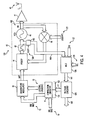
- FIG. 4 An implementation example of a system 120 in accordance with the subject invention is illustrated in FIG. 4 .
- like elements are referenced with like identifying numerals.
- a transmit mode of operation is supported: a transmit mode of operation and a calibration mode of operation.
- memory 123 in correction circuitry 11 contains a value which has been previously determined in the calibration mode of operation in order to reduce or eliminate the unwanted sideband in the output of translation loop 43 .
- a processor 129 within the correction circuitry 11 retrieves the pre-determined value from the memory 123 , and uses the same to correct the complex baseband signal 10 .
- the corrected baseband signal 12 is then upconverted to the desired transmit frequency by quadrature modulator 30 in combination with translation loop 43 .
- This process occurs in two steps. In the first step, the corrected baseband signal 12 is upconverted to VHF frequencies by quadrature modulator 30 using a complex local oscillator signal 13 at VHF frequencies. In the second step, the output signal from the quadrature modulator is upconverted to the desired transmit frequency by translation loop 43 using a second oscillator signal 121 at UHF frequencies.
- the output from the translation loop, signal 122 is then amplified by power amplifier 41 , and the amplified signal transmitted over antenna 42 .
- Translation loop 43 comprises phase detector/charge pump 44 , loop filter 48 , VCO 45 , and downconversion mixer 46 .
- one or more additional filters may be included before or in the loop to perform various functions.
- the output of downconversion mixer 46 is provided as an input to phase detector/charge pump 44 .
- the other input to phase detector/charge pump 44 is the output of quadrature modulator 30 .
- a clipper (not shown) may also be included between the output of the quadrature modulator 30 and the other input to phase detector/charge pump 44 .
- the purpose is to eliminate any AM component of the output of the quadrature modulator 30 .
- the presence of the AM component of the quadrature modulator indicates, as detailed in related co-pending application Ser. No. 09/515,633, the presence of unwanted sideband in the output of the quadrature modulator 30 .
- a filter (not shown) may be included between the output of quadrature modulator 30 and phase detector/charge pump 44 in order to suppress the third harmonic of the transmission intermediate frequency.
- Phase detector/charge pump 44 compares the phase of the signals provided at its two inputs, and outputs a signal having a magnitude proportional to the phase difference between the two input signals.
- the output of phase detector/charge pump 44 is filtered by loop filter 48 , and then provided as an input to VCO 45 .
- the output of VCO 45 is input to the RF input of mixer 46 .
- the frequency of the signal 121 applied to the LO input of mixer 46 , f UHF is such that the sum of f UHF and f VHF , the frequency of the signal 13 applied to the LO input of quadrature modulator 30 , is equal to the desired transmit frequency.
- the output of mixer will have two principal components, one at a relatively low frequency, and the other at a much higher frequency.
- a filter (not shown) may be included at the output of the mixer 46 in order to suppress the higher frequency component.
- the remaining component is provided as an input to phase detector/charge pump 44 .
- Translation loop 43 functions to upconvert the frequency of the signal output from quadrature modulator 30 so that it is at the selected transmit channel frequency.
- the loop functions as follows.
- the output of VCO 45 is provided to mixer 46 .
- Phase detector/charge pump 44 adjusts its output until the phase of the signals at its two inputs are about the same. The effect of this is to adjust the frequency of the output of VCO 45 until this phase relationship is present. This will occur when the frequency at the output of the VCO 45 is equal to f VHV +f UHF , the desired transmit frequency.
- the unwanted sideband detector 16 in this implementation example comprises buffer 143 , multiplexor 126 , and RX chain circuitry 125 .
- the buffer 143 is coupled to the input of VCO 45 .
- the buffer 143 is responsive to a signal POFF, identified with numeral 124 .
- POFF is asserted such that buffer 143 isolates the input to the VCO 45 from signal line 140 .
- the signal POFF is not asserted. Responsive thereto, the buffer 143 couples the input of VCO 45 to signal line 140 .
- Multiplexor 126 and RX chain circuitry 125 function as previously described in relation to the embodiment illustrated in FIG. 2 F.
- the RX chain circuitry 125 forms part of the receiver portion of a transceiver containing system 120 .
- received signal 127 is routed by multiplexor 126 through RX chain circuitry 125 , and output 142 thereof, which is coupled to additional receiver circuitry, is operative.
- this circuitry performs the function of detecting an unwanted sideband in the output 122 of translation loop 43 . Accordingly, in this mode, multiplexor 126 routes signal 140 to RX chain circuitry 125 , and output 17 from this circuitry is operative.
- the presence of an unwanted sideband is detected from the relatively low frequency signal 140 which is taken from the input of VCO 45 .
- a known baseband signal i.e., one having a defined frequency f BB is input to the correction circuitry 11 .
- Processor 129 within correction circuitry 11 delays either the I or Q component of the baseband signal by a known amount ⁇ , which is then stored in the memory 123 .
- the corrected baseband signal is then modulated by quadrature modulator 30 , and the modulated signal input to translational loop 43 .
- Any unwanted sideband in the output of the quadrature modulator will, as previously described, show up in the output 122 of translational loop 43 .
- a low frequency signal will be generated at the input to VCO 45 .
- the unwanted sideband detection circuitry 16 is configured to detect the energy in the signal at the input to the VCO at the frequency f m to provide a direct measure of the energy of the unwanted sideband in the output of the translational loop 43 .
- E unwanted energy of the unwanted sideband at the output of the VCO (and thus at the output of the translational loop)
- E wanted energy at the wanted sideband at the output of the VCO (and thus at the output of the translational loop).
- K vco gain of the VCO (Hertz/V).
- a m energy of the unwanted sideband at the input of the VCO.
- f m frequency offset between the unwanted and wanted sidebands (and thus the frequency offset between the unwanted sideband and DC at the input of the VCO).
- a simple measurement of the low frequency, i.e., baseband, signal at the input of the VCO is easily related to energy of the unwanted sideband in the output of the translational loop. For example, if the governing standard imposes the requirement that the energy of the unwanted sideband should be X dB or more less that the energy of the wanted sideband in the output of the translational loop, then that imposes the following requirement on the system: 20 ⁇ ⁇ log ⁇ ⁇ ( K VCO ⁇ A m 2 ⁇ f m ) ⁇ - X
- the purpose of the calibration mode is to lower A m sufficiently so that the foregoing relationship holds.
- the circuitry 125 comprises buffer 130 , sampling capacitor 131 , RX low pass filter (LPF) 132 , amplifier 133 , and fast Fourier transform (FFT) circuitry 134 .
- LPF RX low pass filter
- FFT fast Fourier transform
- the signal 141 is input to the buffer 130 .
- the output of the buffer 130 drives one input of the RX LPF and sampling capacitor 131 .
- the sampling capacitor 131 stores the DC value of the signal output from buffer 130 , and buffers it to provide the second input to the RX LPF 132 .
- the output of the RX LPF 132 is amplified by amplifier 133 .
- FFT 134 receives the output of the amplifier 133 , and detects the power thereof at a specific frequency, such as f m .
- a signal representative thereof is output on signal line 17 .
- a known baseband signal at 67 kHz is used to calibrate the system. Since f BB is 67 kHz, f m is 134 kHz. In this example, in accordance with GSM standards, the energy of the unwanted sideband in the output of the translational loop should be 43 dB or more less than the energy of the wanted sideband.
- the relative phase ⁇ between the components of the baseband signal is iteratively adjusted until A m is such that 20 ⁇ ⁇ log ⁇ ⁇ ( K VCO ⁇ A m 2 ⁇ f m ) ⁇ - 43.
- the RX LPF 132 and amplifier 133 are set to a 12 dB gain, and the sampling capacitor is 12 pF.
- FFT 134 is configured to detect power at both 134 kHZ and 67 kHz.
- FIG. 3 A a method of forming a transmit signal in accordance with the subject invention is illustrated in FIG. 3 A.
- this embodiment of the method comprises, retrieving, in step 21 , one or more parameters pre-determined to reduce or eliminate an unwanted sideband in the transmit signal; correcting, in step 22 , one or more of BBI and BBQ responsive to the one or more parameters, thereby forming BBI′ and BBQ′; quadrature modulating, in step 23 , BBI′ and BBQ′ respectively with the I and Q components of a local oscillator, LOI and LOQ, to form a modulated signal; deriving, in step 24 , the transmit signal from the modulated signal; and then looping back to step 21 , whereupon the foregoing process may repeat itself one or more times.
- the deriving step comprises upconverting the modulated signal to form the transmit signal.
- a method of calibrating a transmitter comprises correcting, in step 25 , a baseband signal using one or more parameters; modulating, in step 28 , the corrected baseband signal; detecting, in step 26 , an unwanted sideband component in a signal derived from the modulated signal; determining, in decision block 27 , whether the unwanted sideband is below a desired threshold level and if so, storing, in step 34 , the one or more parameters, and then ending the process; if not, in step 29 , adjusting or revising the one or more parameters responsive to the detected unwanted sideband component; and then returning to step 25 , whereupon the foregoing steps may be repeated one or more times until the unwanted sideband component is reduced to an acceptable level.
- the modulated signal is upconverted to a desired transmission frequency
- the detecting step comprises detecting the unwanted sideband from a low frequency signal generated within the translational loop.
- the low frequency signal is generated at the input of a VCO within the translational loop.
- One advantage of the invention is the ability to correct for any inaccuracies in the components of the quadrature modulator.
- Another advantage is the ability to correct for any inaccuracies in the quadrature of the I and Q components of the baseband signal.
- a third advantage is that a highly accurate phase detector is not required.
- a fourth advantage is that correction to a high frequency signal is not required. Instead, the invention only requires correction to the relatively low frequency baseband signal.
- a fifth advantage is detection of unwanted sideband from a high frequency signal is not required. Instead, any unwanted sideband component is detected from a low frequency signal generated within the translation loop of the transmitter.
Abstract
Description


Claims (16)


Priority Applications (1)
| Application Number | Priority Date | Filing Date | Title |
|---|---|---|---|
| US09/514,501 US6658065B1 (en) | 2000-02-29 | 2000-02-29 | System of and method for reducing or eliminating the unwanted sideband in the output of a transmitter comprising a quadrature modulator followed by a translational loop |
Applications Claiming Priority (1)
| Application Number | Priority Date | Filing Date | Title |
|---|---|---|---|
| US09/514,501 US6658065B1 (en) | 2000-02-29 | 2000-02-29 | System of and method for reducing or eliminating the unwanted sideband in the output of a transmitter comprising a quadrature modulator followed by a translational loop |
Publications (1)
| Publication Number | Publication Date |
|---|---|
| US6658065B1 true US6658065B1 (en) | 2003-12-02 |
Family
ID=29550303
Family Applications (1)
| Application Number | Title | Priority Date | Filing Date |
|---|---|---|---|
| US09/514,501 Expired - Lifetime US6658065B1 (en) | 2000-02-29 | 2000-02-29 | System of and method for reducing or eliminating the unwanted sideband in the output of a transmitter comprising a quadrature modulator followed by a translational loop |
Country Status (1)
| Country | Link |
|---|---|
| US (1) | US6658065B1 (en) |
Cited By (11)
| Publication number | Priority date | Publication date | Assignee | Title |
|---|---|---|---|---|
| US20030092414A1 (en) * | 2001-09-05 | 2003-05-15 | Hong Shi | Transmitter method, apparatus, and frequency plan for minimizing spurious energy |
| US20030109233A1 (en) * | 2001-12-07 | 2003-06-12 | Hong Shi | Translational loop transmitter architecture employing channel power ratio measurements for modulation accuracy calibration |
| US20030139148A1 (en) * | 1999-09-14 | 2003-07-24 | Morten Damgaard | Wireless transmitter having a modified translation loop architecture |
| US20030232605A1 (en) * | 2002-06-18 | 2003-12-18 | Meng-An Peng | Single side band transmitter having reduced DC offset |
| US20040043728A1 (en) * | 2002-08-30 | 2004-03-04 | Skyworks Solutions, Inc. | Wireless transmitter incorporating a synchronous oscillator in a translation loop |
| US20040257060A1 (en) * | 2002-11-08 | 2004-12-23 | Rohde & Schwarz Gmbh & Co. Kg | Measuring device and method for determining a characteristic curve of a high frequency unit |
| EP1641131A1 (en) * | 2004-09-24 | 2006-03-29 | Alcatel | Digital sideband suppression for radio frequency (RF) modulators |
| US20060097814A1 (en) * | 2004-11-10 | 2006-05-11 | Alcatel | Digital sideband suppression for radio frequency (RF) modulators |
| US20080116987A1 (en) * | 2006-11-21 | 2008-05-22 | Ryan Gerald P | Method and system for spur supression in modulators |
| US7639769B2 (en) | 2005-04-21 | 2009-12-29 | Agere Systems Inc. | Method and apparatus for providing synchronization in a communication system |
| US20100177902A1 (en) * | 2009-01-15 | 2010-07-15 | King Sum Chu | Audio transmission system |
Citations (10)
| Publication number | Priority date | Publication date | Assignee | Title |
|---|---|---|---|---|
| US5128968A (en) * | 1988-07-27 | 1992-07-07 | Nec Corporation | Apparatus for cancelling carrier phase jitters |
| US5771263A (en) * | 1996-01-08 | 1998-06-23 | Hitachi Denshi Kabushiki Kaisha | Communication system control method and communication system using the method |
| US6028493A (en) * | 1998-04-21 | 2000-02-22 | National Semiconductor Corporation | Elimination of bandpass filter after quadrature modulator in modulation synthesizer circuit |
| US6208875B1 (en) * | 1998-04-08 | 2001-03-27 | Conexant Systems, Inc. | RF architecture for cellular dual-band telephones |
| US6215362B1 (en) * | 1998-06-05 | 2001-04-10 | Siemens Aktiengesellscaft | Phase-locked loop (PLL) for radio-frequency (RF) signals |
| US6278391B1 (en) * | 1998-06-30 | 2001-08-21 | Qualcomm Incorporated | Method and apparatus for D.C. offset correction in digital-to-analog converters |
| US6298096B1 (en) * | 1998-11-19 | 2001-10-02 | Titan Corporation | Method and apparatus for determination of predistortion parameters for a quadrature modulator |
| US6347121B1 (en) * | 1997-03-11 | 2002-02-12 | Erkka Sointula | Transmitting and receiving radio signals |
| US6516184B1 (en) * | 1999-08-31 | 2003-02-04 | Skyworks Solutions, Inc. | Multi-band transceiver having multi-slot capability |
| US6526265B1 (en) * | 1999-09-14 | 2003-02-25 | Skyworks Solutions, Inc. | Wireless transmitter having a modified translation loop architecture |
-
2000
- 2000-02-29 US US09/514,501 patent/US6658065B1/en not_active Expired - Lifetime
Patent Citations (10)
| Publication number | Priority date | Publication date | Assignee | Title |
|---|---|---|---|---|
| US5128968A (en) * | 1988-07-27 | 1992-07-07 | Nec Corporation | Apparatus for cancelling carrier phase jitters |
| US5771263A (en) * | 1996-01-08 | 1998-06-23 | Hitachi Denshi Kabushiki Kaisha | Communication system control method and communication system using the method |
| US6347121B1 (en) * | 1997-03-11 | 2002-02-12 | Erkka Sointula | Transmitting and receiving radio signals |
| US6208875B1 (en) * | 1998-04-08 | 2001-03-27 | Conexant Systems, Inc. | RF architecture for cellular dual-band telephones |
| US6028493A (en) * | 1998-04-21 | 2000-02-22 | National Semiconductor Corporation | Elimination of bandpass filter after quadrature modulator in modulation synthesizer circuit |
| US6215362B1 (en) * | 1998-06-05 | 2001-04-10 | Siemens Aktiengesellscaft | Phase-locked loop (PLL) for radio-frequency (RF) signals |
| US6278391B1 (en) * | 1998-06-30 | 2001-08-21 | Qualcomm Incorporated | Method and apparatus for D.C. offset correction in digital-to-analog converters |
| US6298096B1 (en) * | 1998-11-19 | 2001-10-02 | Titan Corporation | Method and apparatus for determination of predistortion parameters for a quadrature modulator |
| US6516184B1 (en) * | 1999-08-31 | 2003-02-04 | Skyworks Solutions, Inc. | Multi-band transceiver having multi-slot capability |
| US6526265B1 (en) * | 1999-09-14 | 2003-02-25 | Skyworks Solutions, Inc. | Wireless transmitter having a modified translation loop architecture |
Non-Patent Citations (1)
| Title |
|---|
| Moffat, Mark, et al., An ISM band Transceiver Chip for Digital Spread Spectrum Communication, GEC Plessey Semiconductors, Inc., Scotts Valley, CA 95067, USA. |
Cited By (27)
| Publication number | Priority date | Publication date | Assignee | Title |
|---|---|---|---|---|
| US20030139148A1 (en) * | 1999-09-14 | 2003-07-24 | Morten Damgaard | Wireless transmitter having a modified translation loop architecture |
| US6952569B2 (en) * | 1999-09-14 | 2005-10-04 | Skyworks Solutions, Inc. | Wireless transmitter having a modified translation loop architecture |
| US20030092414A1 (en) * | 2001-09-05 | 2003-05-15 | Hong Shi | Transmitter method, apparatus, and frequency plan for minimizing spurious energy |
| US6868261B2 (en) * | 2001-09-05 | 2005-03-15 | Broadcom Corporation | Transmitter method, apparatus, and frequency plan for minimizing spurious energy |
| US7471934B2 (en) | 2001-09-05 | 2008-12-30 | Broadcom Corporation | Transmitter method, apparatus, and frequency plan for minimizing spurious energy |
| US20050113053A1 (en) * | 2001-09-05 | 2005-05-26 | Broadcom Corporation | Transmitter method, apparatus, and frequency plan for minimizing spurious energy |
| US20050153670A1 (en) * | 2001-12-07 | 2005-07-14 | Hong Shi | Translational loop transmitter architecture employing channel power ratio measurements for modulation accuracy calibration |
| US6882831B2 (en) * | 2001-12-07 | 2005-04-19 | Broadcom Corporation | Translational loop transmitter architecture employing channel power ratio measurements for modulation accuracy calibration |
| US8112045B2 (en) * | 2001-12-07 | 2012-02-07 | Broadcom Corporation | Translational loop transmitter architecture employing channel power ratio measurements for modulation accuracy calibration |
| US20030109233A1 (en) * | 2001-12-07 | 2003-06-12 | Hong Shi | Translational loop transmitter architecture employing channel power ratio measurements for modulation accuracy calibration |
| US20090093224A1 (en) * | 2001-12-07 | 2009-04-09 | Broadcom Corporation | Translational loop transmitter architecture employing channel power ratio measurements for modulation accuracy calibration |
| US7499680B2 (en) * | 2001-12-07 | 2009-03-03 | Broadcom Corporation | Translational loop transmitter architecture employing channel power ratio measurements for modulation accuracy calibration |
| US20030232605A1 (en) * | 2002-06-18 | 2003-12-18 | Meng-An Peng | Single side band transmitter having reduced DC offset |
| US7103327B2 (en) * | 2002-06-18 | 2006-09-05 | Broadcom, Corp. | Single side band transmitter having reduced DC offset |
| US6961547B2 (en) * | 2002-08-30 | 2005-11-01 | Skyworks Solutions, Inc. | Wireless transmitter incorporating a synchronous oscillator in a translation loop |
| US20040043728A1 (en) * | 2002-08-30 | 2004-03-04 | Skyworks Solutions, Inc. | Wireless transmitter incorporating a synchronous oscillator in a translation loop |
| US6973401B2 (en) * | 2002-11-08 | 2005-12-06 | Rohde & Schwarz Gmbh & Co. Kg | Measuring device and method for determining a characteristic curve of a high frequency unit |
| US20040257060A1 (en) * | 2002-11-08 | 2004-12-23 | Rohde & Schwarz Gmbh & Co. Kg | Measuring device and method for determining a characteristic curve of a high frequency unit |
| US20060067425A1 (en) * | 2004-09-24 | 2006-03-30 | Alcatel | Transmitter and transmission method |
| CN100459441C (en) * | 2004-09-24 | 2009-02-04 | 阿尔卡特公司 | Transmitter and transmission method |
| EP1641132A1 (en) * | 2004-09-24 | 2006-03-29 | Alcatel | transmitter and transmission method |
| EP1641131A1 (en) * | 2004-09-24 | 2006-03-29 | Alcatel | Digital sideband suppression for radio frequency (RF) modulators |
| US20060097814A1 (en) * | 2004-11-10 | 2006-05-11 | Alcatel | Digital sideband suppression for radio frequency (RF) modulators |
| US7639769B2 (en) | 2005-04-21 | 2009-12-29 | Agere Systems Inc. | Method and apparatus for providing synchronization in a communication system |
| US20080116987A1 (en) * | 2006-11-21 | 2008-05-22 | Ryan Gerald P | Method and system for spur supression in modulators |
| US7570127B2 (en) * | 2006-11-21 | 2009-08-04 | Arris Group, Inc. | Method and system for spur suppression in modulators |
| US20100177902A1 (en) * | 2009-01-15 | 2010-07-15 | King Sum Chu | Audio transmission system |
Similar Documents
| Publication | Publication Date | Title |
|---|---|---|
| US6516184B1 (en) | Multi-band transceiver having multi-slot capability | |
| US6526265B1 (en) | Wireless transmitter having a modified translation loop architecture | |
| US6658237B1 (en) | Multi-Band transceiver utilizing direct conversion receiver | |
| US6671500B2 (en) | Frequency plan | |
| US6804261B2 (en) | Multi-band receiver having multi-slot capability | |
| US7499680B2 (en) | Translational loop transmitter architecture employing channel power ratio measurements for modulation accuracy calibration | |
| US6658065B1 (en) | System of and method for reducing or eliminating the unwanted sideband in the output of a transmitter comprising a quadrature modulator followed by a translational loop | |
| GB2258122A (en) | Detecting intermodulation distortion in a radio frequency receiver | |
| US7031676B2 (en) | Radio frequency transmitter having translational loop phase equalization | |
| US7283794B2 (en) | Low voltage digital interface | |
| US6720839B1 (en) | System of and method for reducing or eliminating the unwanted sideband in a signal derived from the output of a quadrature modulator | |
| US6731693B1 (en) | System of and method for compensating a baseband signal to reduce third order modulation distortion | |
| US20140154998A1 (en) | Transmit Adaptation Responsive to Signal Transformation | |
| EP1419597B1 (en) | Method and device for enhancing quality of signal transmission |
Legal Events
| Date | Code | Title | Description |
|---|---|---|---|
| AS | Assignment |
Owner name: CONEXANT SYSTEMS, INC., CALIFORNIA Free format text: ASSIGNMENT OF ASSIGNORS INTEREST;ASSIGNORS:DELLA TORRE, VALENTINA;STUBBE, FREDERIC M.;AHMED, KASHIF A.;AND OTHERS;REEL/FRAME:010779/0173;SIGNING DATES FROM 20000424 TO 20000501 |
|
| AS | Assignment |
Owner name: ALPHA INDUSTRIES, INC., MASSACHUSETTS Free format text: MERGER;ASSIGNOR:WASHINGTON SUB, INC.;REEL/FRAME:013288/0249 Effective date: 20020625 Owner name: SKYWORKS SOLUTIONS, INC., CALIFORNIA Free format text: ASSIGNMENT OF ASSIGNORS INTEREST;ASSIGNOR:ALPHA INDUSTRIES, INC.;REEL/FRAME:013288/0241 Effective date: 20020625 Owner name: WASHINGTON SUB, INC., CALIFORNIA Free format text: ASSIGNMENT OF ASSIGNORS INTEREST;ASSIGNOR:CONEXANT SYSTEMS, INC.;REEL/FRAME:013288/0197 Effective date: 20020625 |
|
| AS | Assignment |
Owner name: CONEXANT SYSTEMS, INC., CALIFORNIA Free format text: SECURITY INTEREST;ASSIGNOR:ALPHA INDUSTRIES, INC.;REEL/FRAME:013240/0860 Effective date: 20020625 |
|
| AS | Assignment |
Owner name: SKYWORKS SOLUTIONS, INC., CALIFORNIA Free format text: CORRECTIVE MERGER ON REEL 013288 FRAME 0241 TO DELETE S/N 09/811,082 AND 09/793,744;ASSIGNOR:ALPHA INDUSTRIES, INC.;REEL/FRAME:013645/0527 Effective date: 20020626 |
|
| AS | Assignment |
Owner name: ALPHA INDUSTRIES, INC., MASSACHUSETTS Free format text: RELEASE AND RECONVEYANCE/SECURITY INTEREST;ASSIGNOR:CONEXANT SYSTEMS, INC.;REEL/FRAME:014580/0880 Effective date: 20030307 |
|
| STCF | Information on status: patent grant |
Free format text: PATENTED CASE |
|
| FPAY | Fee payment |
Year of fee payment: 4 |
|
| FEPP | Fee payment procedure |
Free format text: PAYOR NUMBER ASSIGNED (ORIGINAL EVENT CODE: ASPN); ENTITY STATUS OF PATENT OWNER: LARGE ENTITY Free format text: PAYER NUMBER DE-ASSIGNED (ORIGINAL EVENT CODE: RMPN); ENTITY STATUS OF PATENT OWNER: LARGE ENTITY |
|
| FPAY | Fee payment |
Year of fee payment: 8 |
|
| FPAY | Fee payment |
Year of fee payment: 12 |