US6655966B2 - Modular connector with grounding interconnect - Google Patents
Modular connector with grounding interconnect Download PDFInfo
- Publication number
- US6655966B2 US6655966B2 US10/100,822 US10082202A US6655966B2 US 6655966 B2 US6655966 B2 US 6655966B2 US 10082202 A US10082202 A US 10082202A US 6655966 B2 US6655966 B2 US 6655966B2
- Authority
- US
- United States
- Prior art keywords
- signal modules
- ground planes
- connector assembly
- electrical connector
- signal
- Prior art date
- Legal status (The legal status is an assumption and is not a legal conclusion. Google has not performed a legal analysis and makes no representation as to the accuracy of the status listed.)
- Expired - Lifetime
Links
Images


Classifications
-
- H—ELECTRICITY
- H01—ELECTRIC ELEMENTS
- H01R—ELECTRICALLY-CONDUCTIVE CONNECTIONS; STRUCTURAL ASSOCIATIONS OF A PLURALITY OF MUTUALLY-INSULATED ELECTRICAL CONNECTING ELEMENTS; COUPLING DEVICES; CURRENT COLLECTORS
- H01R13/00—Details of coupling devices of the kinds covered by groups H01R12/70 or H01R24/00 - H01R33/00
- H01R13/648—Protective earth or shield arrangements on coupling devices, e.g. anti-static shielding
-
- H—ELECTRICITY
- H01—ELECTRIC ELEMENTS
- H01R—ELECTRICALLY-CONDUCTIVE CONNECTIONS; STRUCTURAL ASSOCIATIONS OF A PLURALITY OF MUTUALLY-INSULATED ELECTRICAL CONNECTING ELEMENTS; COUPLING DEVICES; CURRENT COLLECTORS
- H01R13/00—Details of coupling devices of the kinds covered by groups H01R12/70 or H01R24/00 - H01R33/00
- H01R13/646—Details of coupling devices of the kinds covered by groups H01R12/70 or H01R24/00 - H01R33/00 specially adapted for high-frequency, e.g. structures providing an impedance match or phase match
- H01R13/6461—Means for preventing cross-talk
- H01R13/6471—Means for preventing cross-talk by special arrangement of ground and signal conductors, e.g. GSGS [Ground-Signal-Ground-Signal]
-
- H—ELECTRICITY
- H01—ELECTRIC ELEMENTS
- H01R—ELECTRICALLY-CONDUCTIVE CONNECTIONS; STRUCTURAL ASSOCIATIONS OF A PLURALITY OF MUTUALLY-INSULATED ELECTRICAL CONNECTING ELEMENTS; COUPLING DEVICES; CURRENT COLLECTORS
- H01R13/00—Details of coupling devices of the kinds covered by groups H01R12/70 or H01R24/00 - H01R33/00
- H01R13/648—Protective earth or shield arrangements on coupling devices, e.g. anti-static shielding
- H01R13/658—High frequency shielding arrangements, e.g. against EMI [Electro-Magnetic Interference] or EMP [Electro-Magnetic Pulse]
- H01R13/6581—Shield structure
- H01R13/6585—Shielding material individually surrounding or interposed between mutually spaced contacts
- H01R13/6586—Shielding material individually surrounding or interposed between mutually spaced contacts for separating multiple connector modules
-
- H—ELECTRICITY
- H01—ELECTRIC ELEMENTS
- H01R—ELECTRICALLY-CONDUCTIVE CONNECTIONS; STRUCTURAL ASSOCIATIONS OF A PLURALITY OF MUTUALLY-INSULATED ELECTRICAL CONNECTING ELEMENTS; COUPLING DEVICES; CURRENT COLLECTORS
- H01R12/00—Structural associations of a plurality of mutually-insulated electrical connecting elements, specially adapted for printed circuits, e.g. printed circuit boards [PCB], flat or ribbon cables, or like generally planar structures, e.g. terminal strips, terminal blocks; Coupling devices specially adapted for printed circuits, flat or ribbon cables, or like generally planar structures; Terminals specially adapted for contact with, or insertion into, printed circuits, flat or ribbon cables, or like generally planar structures
- H01R12/70—Coupling devices
- H01R12/71—Coupling devices for rigid printing circuits or like structures
- H01R12/72—Coupling devices for rigid printing circuits or like structures coupling with the edge of the rigid printed circuits or like structures
- H01R12/722—Coupling devices for rigid printing circuits or like structures coupling with the edge of the rigid printed circuits or like structures coupling devices mounted on the edge of the printed circuits
- H01R12/724—Coupling devices for rigid printing circuits or like structures coupling with the edge of the rigid printed circuits or like structures coupling devices mounted on the edge of the printed circuits containing contact members forming a right angle
Definitions
- Certain embodiments of the present invention generally relate to electrical connectors, and more particularly to high-speed high-density board-to-board connectors.
- Modular connectors exist for connecting various types of circuit boards, such as daughter cards, mother boards, back planes and the like.
- the modular connectors convey a densely packed number of signal lines between the circuit boards.
- the modular connectors each include multiple wafers or signal modules stacked in parallel.
- the wafers have two sides that have ground planes and signal lines formed thereon.
- the signal lines carry data between mating ends of the wafers, and the ground planes control impedance.
- the signal lines may be arranged on adjacent wafers to form differential pairs.
- differential pair applications a signal is divided and transmitted in a first direction over a pair of conductors (and hence through a pair of pins or contacts).
- a return signal is similarly divided and transmitted in an opposite direction over the same pair of conductors (and hence through the same pair of pins or contacts).
- two signal lines on adjacent wafers may form a differential pair and carry a divided signal along the two signal lines.
- Line density is a measure of differential pairs per linear inch measured along the direction perpendicular to the wafers.
- increasing the data rates and line density increases insertion loss and cross talk between signal lines.
- Ground planes reduce interference between signal lines and therefore decrease insertion loss and cross talk.
- An embodiment of the present invention provides an electrical connector having a connector housing with signal modules and grounding members therein.
- Each signal module has a ground plane on at least one side thereof.
- the ground planes have contact pads formed at opposite ends thereof proximate mating ends of the signal modules.
- the grounding members interconnect the ground planes on adjacent signal modules to one another at a point along the ground planes or the contact pads.
- the signal modules may be printed circuit boards.
- the signal modules may be pieces of molded plastic with metal traces mounted thereon.
- the signal modules may include vias having conductive liners therethrough that electrically connect ground planes on opposite sides of a signal module.
- the signal modules may be arranged parallel to one another within the housing.
- Each signal module may have one or more ground planes and one or more signal lines.
- adjacent signal modules may have signal lines facing one another and forming differential pairs.
- the grounding member may include pins adjoining two or more vias on two or more signal modules to one another.
- the grounding member may be a conductive rod that extends through a plurality of vias in a plurality of signal modules.
- the grounding member may be a metal object interposed between adjacent signal modules and may have one of spring members, dimples and beams that contact ground planes on the adjacent modules.
- the grounding member may be a metal rack having slots cut therein for receiving signal modules, where the signal modules include projections contacting ground planes on the signal modules.
- An advantage of certain embodiments of the present invention is that the connector can carry large amounts of data quickly and in a very high line density with reduced insertion loss and cross talk. Because the ground planes are electrically interconnected within the connector housing by the conductive liners of the vias and the grounding members, the development of local potentials on the ground planes is minimized, thereby reducing insertion loss rates and cross talk between signal lines.
- FIG. 1 illustrates a top front perspective view of a connector assembly formed in accordance with an embodiment of the present invention.
- FIG. 2 illustrates a bottom rear perspective view of a connector assembly formed in accordance with an alternative embodiment of the present invention.
- FIG. 3 illustrates a top rear perspective view of a connector assembly formed in accordance with an alternative embodiment of the present invention.
- FIG. 4 illustrates a top rear perspective view of a connector assembly formed in accordance with an alternative embodiment of the present invention.
- FIG. 5 illustrates a top rear perspective view of a signal module and a grounding bracket formed in accordance with an embodiment of the present invention.
- FIG. 6 illustrates a bottom front perspective view of a grounding plate formed in accordance with an embodiment of the present invention.
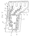
- FIG. 7 illustrates a top front perspective view of the grounding plate of FIG. 6 joined with a signal module in accordance with an embodiment of the present invention.
- FIG. 8 illustrates a right side plan view of a signal module formed in accordance with an embodiment of the present invention
- FIG. 9 illustrates a left side plan view of a signal module formed in accordance with an embodiment of the present invention.
- FIG. 10 illustrates a bottom front perspective view of a grounding plate formed in accordance with an embodiment of the present invention.
- FIG. 11 illustrates a bottom front perspective view of a grounding plate formed in accordance with an embodiment of the present invention.
- FIG. 12 illustrates a top rear perspective view of a connector assembly with an inter-connector assembly grounding clip formed in accordance with an embodiment of the resent invention.
- FIG. 13 illustrates a top rear perspective view of a connector assembly with an inter-connector assembly grounding clip formed in accordance with an alternative embodiment of the present invention.
- FIG. 14 illustrates a graph of insertion loss performance of a right angle connector assembly not formed in accordance with an embodiment of the present invention.
- FIG. 15 illustrates a graph of insertion loss performance of a right angle connector assembly formed in accordance with an embodiment of the present invention.
- FIG. 1 illustrates a plug 2 formed in accordance with an embodiment of the present invention.
- the plug 2 is configured to mate with a receptacle (not shown) to form a right angle connector assembly (not shown).
- the plug 2 includes a connector housing 4 and a plurality of signal modules 6 mounted therein.
- the signal modules 6 are arranged parallel to one another and spaced apart by gaps 8 .
- the signal modules 6 include mating ends 10 and 12 formed at right angles to one another.
- the mating end 10 includes pads 14 for mating with a contact (not visible) that has a pin 16 extending downward therefrom.
- the pin 16 is configured to be inserted into a via in a daughter printed circuit board (PCB) (not shown).
- PCB daughter printed circuit board
- the mating end 12 includes pads 18 that are configured to mate with a back plane PCB (not shown).
- the signal modules include side surfaces 20 and 22 that have ground planes 24 and signal lines 28 .
- each of the signal modules 6 includes six ground planes 24 and four signal lines 28 .
- Each of the signal modules 6 also includes a drill hole 32 for location purposes during manufacturing and a plurality of holes or vias 34 .
- the vias 34 include conductive liners 36 that electrically connect the ground planes 24 on the side surfaces 20 and 22 of each signal module 6 to one another.
- grounding rods 38 are inserted through selected vias 34 in at least two signal modules 6 .
- the grounding rods 38 electrically inter-connect the ground planes 24 of different signal modules 6 to one another.
- FIG. 2 illustrates a plug 42 formed in accordance with an alternative embodiment of the present invention.
- the plug 42 includes connector housings 44 and 46 (unmated in FIG. 2 ).
- the connector housing 44 includes top and rear walls 48 and 50 that hold a plurality of signal modules 52 arranged parallel to one another and spaced apart at gaps 54 .
- the signal modules 52 include ground planes 56 and signal lines 58 arranged on both sides 60 , 62 of the signal modules 52 .
- the ground planes 56 include pads 64 that are located proximate mating ends 66 of the signal modules 52 .
- the signal modules 52 also include vias 68 having conductive liners therethrough that electrically connect the ground planes 56 on opposite sides 60 and 62 of the signal modules 52 to one another.
- the connector housing 46 includes front and bottom walls 70 and 72 that join with the top and rear walls 48 and 50 .
- the bottom wall 72 includes channels 74 extending along a length thereof for receiving bottom edges 76 of the signal modules 52 .
- the front wall 70 includes slots 78 for receiving mating ends 66 of the signal modules 52 .
- the front wall 70 includes plastic rails 80 located between, and along, the slots 78 and having contact brackets 82 clasped thereto.
- the contact brackets 82 include a flat body section 84 having flat legs 86 that clasp the rails 80 .
- the slots 78 receive the mating ends 66 of the signal modules 52
- the flat legs 86 of the contact brackets 82 engage the ground planes 56 .
- each of the contact brackets 82 is electrically connected to the ground planes 56 of two adjacent of the signal modules 52 .
- FIG. 3 illustrates a plug 90 formed in accordance with an alternative embodiment of the present invention.
- the plug 90 includes connector housings 92 and 94 .
- the connector housing 92 includes signal modules 96 therein.
- the signal modules 96 include side surfaces 98 having ground planes 100 and signal lines 102 formed thereon.
- the signal modules 96 are held within a conductive plate 104 having flat parallel bars 106 separated by parallel slots 108 cut therebetween.
- the slots 108 receive the signal modules 96 so that the planes of the signal modules 96 are perpendicular to the plane of the conductive plate 104 .
- the bars 106 include compliant fingers 110 extending horizontally therefrom and bending towards mating ends 112 of the signal modules 96 .
- the compliant fingers 110 engage, and electrically interconnect, the ground planes 100 of the signal modules 96 .
- all of the ground planes 100 are electrically connected to one another.
- FIG. 4 illustrates a plug 114 formed in accordance with an alternative embodiment of the present invention.
- the plug 114 includes connector housings 116 and 118 .
- the connector housing 116 includes signal modules 120 and a U-shaped grounding jacket 122 therein.
- the connector housing 116 includes front and bottom walls 124 and 126 that are aligned perpendicular to one another.
- the front and bottom walls 124 and 126 include L-shaped channels 128 (only partially visible) for receiving the signal modules 120 .
- the channels 128 turn 90 degrees at a juncture 130 between the front and bottom walls 124 and 126 .
- the signal modules 120 include side surfaces 132 having ground planes 134 and signal lines 136 formed thereon.
- the grounding jacket 122 includes front and back walls 138 and 140 that are aligned parallel to one another and spaced apart.
- the front and back walls 138 and 140 are joined together by a bottom wall 139 .
- the walls 138 - 140 include parallel slots 142 cut therethrough and spaced apart by flat bars 144 .
- the slots 142 are aligned with the channels 128 and receive the signal modules 120 .
- the flat bars 144 include semicircular projections 146 protruding into the slots 142 and engaging, and electrically interconnecting, the ground planes 134 on the signal modules 120 .
- FIG. 5 illustrates a signal module 150 adjacent to and engaged with a U-shaped grounding bracket 152 formed in accordance with an embodiment of the present invention.
- the signal module 150 includes vias 154 having conductive liners 156 therethrough.
- the signal module 150 also includes side surfaces 158 , 160 having ground planes 162 and signal lines 164 formed thereon.
- the grounding bracket 152 includes planar sidewalls 166 and 168 aligned parallel to, and separated from, one another, and joined by a bottom wall 170 .
- the sidewalls 166 and 168 include extruded dimples 172 protruding outward in a direction perpendicular to, and away from, both of the sidewalls 166 and 168 .
- the dimples 172 engage the ground planes 162 of the signal module 150 , thereby electrically interconnecting the ground planes 162 on the side surface 158 .
- the ground planes 162 on the side surface 160 are electrically connected to the ground planes 162 on the side surface 158 through the conductive liners 156 of the vias 154 .
- all of the ground planes 162 of the signal module 150 are electrically connected to one another.
- the signal module 150 and grounding bracket 152 can be stacked into a connector housing (not shown) in an alternating arrangement of signal modules 150 and metal brackets 152 so that all of the ground planes 162 of several signal modules 150 are electrically interconnected with one another. In such an arrangement, friction between the dimples 172 and the ground planes 162 retains the metal brackets 152 in position.
- FIG. 6 illustrates a grounding plate 174 formed in accordance with an embodiment of the present invention.
- the grounding plate 174 is for insertion between parallel signal modules (not shown) and can be mounted on a signal module.
- the grounding plate 174 includes a flat body section 176 .
- the flat body section 176 includes via-engaging beams 178 extending therefrom in a direction perpendicular to the plane of the flat body section 176 .
- the flat body section 176 also includes ground-plane engaging beams 180 extending therefrom at acute angles to the plane of the flat body section 176 .
- the ground-plane engaging beams 180 bend away from the flat body section 176 in a direction opposite to a direction in which the via-engaging beams 178 extend.
- FIG. 7 illustrates a signal module 182 with the metal plate 174 mounted thereon.
- the signal module 182 includes a drill hole 184 for location purposes during manufacturing.
- the signal module 182 also has side surfaces 186 and 188 that have ground planes 190 and signal lines 192 formed thereon.
- the ground planes 190 include vias 194 that extend through the signal module 182 .
- the vias 194 have conductive liners 196 therethrough that electrically connect the ground planes 190 on the side surface 186 to the ground planes 190 on the side surface 188 .
- the via-engaging beams 178 of the metal plate 174 are inserted into selected vias 194 on the side surface 186 , thereby electrically connecting and physically attaching the metal plate 174 to the ground planes 190 .
- all of the ground planes 190 of the signal module 182 are electrically connected to one another.
- additional metal plates 174 and signal modules 182 can be stacked into a connector housing (not shown) in an alternating arrangement so that all of the ground planes 190 of the multiple signal modules 182 are electrically interconnected with one another.
- the ground plane-engaging beams 180 of the metal plates 174 contact the ground planes 190 on the side surfaces 188 of the signal modules 182 .
- the ground plane-engaging beams 180 of each of the metal plates 174 would be electrically connected, but not physically attached, to the ground planes 190 of the side surface 188
- the via-engaging beams 178 of each of the metal plates 174 would be electrically connected, and physically attached, to the ground planes 190 of the side surface 186 .
- FIG. 8 illustrates a right side plan view of a signal module 200 formed in accordance with an embodiment of the present invention.
- the signal module 200 includes mating ends 202 and 204 that are aligned perpendicular to one another and have pads 206 for mating with contacts (not shown).
- the signal module 200 includes a drill hole 207 for location purposes during manufacturing.
- the signal module 200 also includes a side surface 208 that has ground planes 210 - 212 and signal lines 214 and 216 .
- the signal line 214 is located between the ground planes 210 and 211
- the signal line 216 is located between the ground planes 211 and 212 .
- the ground planes 210 - 212 include vias 218 that have conductive lining extending through the vias 218 .
- FIG. 9 illustrates a left side plan view of the signal module 200 .
- the signal module 200 includes a side surface 222 opposite to the side surface 208 .
- the side surface 222 includes ground planes 224 - 226 and signal lines 228 and 230 .
- the signal line 228 is located between the ground planes 224 and 225
- the signal line 230 is located between the ground planes 225 and 226 .
- the conductive lining that extends through the vias 218 electrically connects the ground planes 210 - 212 of the side surface 208 to the ground planes 224 - 226 of the side surface 222 .
- the ground plane 210 is electrically connected to the ground plane 224
- the ground plane 211 is electrically connected to the ground planes 224 and 225
- the ground plane 212 is electrically connected to the ground planes 225 and 226 .
- FIG. 10 illustrates a grounding contact 232 , for insertion between signal modules 200 stacked in a parallel arrangement (not shown), formed in accordance with an embodiment of the present invention.
- the grounding contact 232 is a stamped strip of metal having rectangular ends 234 and 236 configured to be inserted into slots in a connector housing (not shown).
- the grounding contact 232 includes a height 238 , width 240 , and thickness 242 .
- the grounding contact 232 includes spring elements 244 having rounded ends 246 that extend outward beyond the width 240 of the grounding contact 232 .
- the rounded ends 246 of the spring elements 244 engage the ground planes 210 - 212 and 224 - 226 of the signal modules 200 , thereby electrically connecting the ground planes 210 - 212 on the side surfaces 208 of the signal modules 200 to the ground planes 224 - 226 on the side surfaces 222 of adjacent signal modules 200 .
- FIG. 11 illustrates a bottom front view of a grounding contact 248 , for insertion between signal modules 200 stacked in a parallel arrangement (not shown), formed in accordance with an embodiment of the present invention.
- the grounding contact 248 is a stamped strip of metal having a planar body section 250 and rectangular ends 252 and 254 configured to be inserted into slots in a connector housing (not shown).
- the grounding contact 248 includes edges 256 and 258 extending vertically from the end 252 to the end 254 .
- the edges 256 and 258 include compliant beams 260 - 265 extending outward horizontally therefrom and at angles to the planar body section 250 of the grounding contact 248 .
- the compliant beams 260 - 265 include curved ends 268 for engaging the ground planes 210 - 212 and 224 - 226 of the signal modules 200 .
- the curved ends 268 of the compliant beams 260 - 265 engage the ground planes 210 - 212 and 224 - 226 of the signal modules 200 , thereby electrically connecting the ground planes 210 - 212 on the side surfaces 208 of the signal modules 200 to the ground planes 224 - 226 on the side surfaces 222 of adjacent signal modules 200 .
- FIG. 12 illustrates a plug 270 formed in accordance with an alternative embodiment of the present invention.
- the plug 270 includes mated connector housings 272 and 274 having a plurality of signal modules 276 aligned parallel to one another therein.
- the plug 270 includes sides 278 and 280 .
- the side 278 includes an inter-connector assembly grounding clip 282 .
- the grounding clip 282 includes two zigzagged bars 284 and 286 .
- the bar 284 includes corners 288 - 290 protruding inward toward, and contacting, ground planes 292 on the signal module 276 that is most closely located to the side 278 .
- the bar 286 includes corners 294 - 296 protruding outward away from the corners 288 - 290 and configured to the contact ground planes 292 on a signal module 276 in an adjacent plug 270 , thereby electrically interconnecting the ground planes 292 of signal modules 276 on adjacent plugs 270 .
- FIG. 13 illustrates a plug 300 formed in accordance with an embodiment of the present invention.
- the plug 300 includes mated connector housings 302 and 304 having a plurality of signal modules 306 aligned parallel to one another therein.
- the plug 300 includes sides 308 and 310 .
- the side 308 includes an inter-connector assembly grounding clip 312 .
- the grounding clip 312 includes three flat beams 314 - 316 . 316 .
- the beams 314 and 316 include buckles 318 protruding inward toward, and contacting, the ground planes 320 on the signal module 306 that is most closely located to the side 308 .
- the middle beam 315 is bent outward away from the connector assembly 300 and is configured to contact a middle beam 315 of a grounding clip 312 on a side 310 of an adjacent plug 300 , thereby electrically interconnecting the ground planes 320 of adjacent plugs 300 .
- FIG. 14 illustrates a graph of insertion loss performance of a right angle connector assembly not formed in accordance with an embodiment of the present invention.
- the graph depicts insertion loss measured in dB along a y-axis versus fundamental frequency of a transmitted signal measured in GHz along an x-axis.
- the insertion loss is equal to 20 times the log base 10 of (voltage output/voltage input).
- Voltage input is the measure in volts of the signal input at one end of a signal line
- voltage output is the measure in volts of the signal output at an opposite end of the signal line.
- the fundamental frequency increases from 0.00 to 5.00 GHz, the absolute value of insertion loss increases.
- the absolute value of insertion loss As the fundamental frequency increases from 5.00 to 6.00 GHz, the absolute value of insertion loss generally increases, but along ranges 322 and 324 , the absolute value of insertion loss decreases. At a fundamental frequency of 4.00 GHz, the absolute value of insertion loss is greater than 1.00 dB 326 . At a fundamental frequency of 5.00 GHz, the absolute value of insertion loss is about 2.50 dB 328 . At a fundamental frequency of 6.00 GHz, the absolute value of insertion loss is about 4.00 dB 330 .
- FIG. 15 illustrates a graph of insertion loss performance of a right angle connector assembly formed in accordance with an embodiment of the present invention.
- the graph depicts insertion loss measured in dB along a y-axis versus fundamental frequency measured in GHz along an x-axis.
- the absolute value of insertion loss increases.
- the absolute value of insertion loss is less than 1.00 dB 332 .
- the absolute value of insertion loss is less than 1.50 dB 334 .
- the absolute value of insertion loss is still less than 1.50 dB 336 .
- While certain embodiments of the present invention employ plugs for right angle connector assemblies, other embodiments may include plugs for straight or orthogonal connector assemblies.
- While certain embodiments of the present invention employ plugs for connector assemblies, other embodiments may include receptacles for connector assemblies.
Abstract
Description
Claims (20)
Priority Applications (7)
| Application Number | Priority Date | Filing Date | Title |
|---|---|---|---|
| US10/100,822 US6655966B2 (en) | 2002-03-19 | 2002-03-19 | Modular connector with grounding interconnect |
| PCT/US2003/008057 WO2003081726A1 (en) | 2002-03-19 | 2003-03-14 | Modular connector with grounding interconnect |
| CNB038100037A CN100334779C (en) | 2002-03-19 | 2003-03-14 | Modular connector with grounding interconnect |
| AU2003220324A AU2003220324A1 (en) | 2002-03-19 | 2003-03-14 | Modular connector with grounding interconnect |
| KR10-2004-7014805A KR20040094826A (en) | 2002-03-19 | 2003-03-14 | Modular connector with grounding interconnect |
| JP2003579320A JP2005521224A (en) | 2002-03-19 | 2003-03-14 | Modular connector with ground interconnection member |
| DE10392400T DE10392400T5 (en) | 2002-03-19 | 2003-03-14 | Modular connector with grounding interconnections |
Applications Claiming Priority (1)
| Application Number | Priority Date | Filing Date | Title |
|---|---|---|---|
| US10/100,822 US6655966B2 (en) | 2002-03-19 | 2002-03-19 | Modular connector with grounding interconnect |
Publications (2)
| Publication Number | Publication Date |
|---|---|
| US20030181077A1 US20030181077A1 (en) | 2003-09-25 |
| US6655966B2 true US6655966B2 (en) | 2003-12-02 |
Family
ID=28039908
Family Applications (1)
| Application Number | Title | Priority Date | Filing Date |
|---|---|---|---|
| US10/100,822 Expired - Lifetime US6655966B2 (en) | 2002-03-19 | 2002-03-19 | Modular connector with grounding interconnect |
Country Status (7)
| Country | Link |
|---|---|
| US (1) | US6655966B2 (en) |
| JP (1) | JP2005521224A (en) |
| KR (1) | KR20040094826A (en) |
| CN (1) | CN100334779C (en) |
| AU (1) | AU2003220324A1 (en) |
| DE (1) | DE10392400T5 (en) |
| WO (1) | WO2003081726A1 (en) |
Cited By (81)
| Publication number | Priority date | Publication date | Assignee | Title |
|---|---|---|---|---|
| US20030077922A1 (en) * | 2001-10-23 | 2003-04-24 | Tsutomu Matsuo | Intermediate board electrical connector |
| US6808419B1 (en) * | 2003-08-29 | 2004-10-26 | Hon Hai Precision Ind. Co., Ltd. | Electrical connector having enhanced electrical performance |
| US6808399B2 (en) * | 2002-12-02 | 2004-10-26 | Tyco Electronics Corporation | Electrical connector with wafers having split ground planes |
| US20050048817A1 (en) * | 2003-09-03 | 2005-03-03 | Cohen Thomas S. | High speed, high density electrical connector |
| US20050048838A1 (en) * | 2003-08-29 | 2005-03-03 | Korsunsky Iosif R. | Electrical connector having circuit board modules positioned between metal stiffener and a housing |
| US6875031B1 (en) * | 2003-12-05 | 2005-04-05 | Hon Hai Precision Ind. Co., Ltd. | Electrical connector with circuit board module |
| US6932649B1 (en) * | 2004-03-19 | 2005-08-23 | Tyco Electronics Corporation | Active wafer for improved gigabit signal recovery, in a serial point-to-point architecture |
| US20060135253A1 (en) * | 2004-09-10 | 2006-06-22 | Jeffrey George | Gaming system and method for providing entry to a contest |
| US20080214055A1 (en) * | 2006-12-20 | 2008-09-04 | Gulla Joseph M | Electrical connector assembly |
| US20090023320A1 (en) * | 2007-07-20 | 2009-01-22 | Numatics, Incorporated | Modular electrical bus system |
| US20090186533A1 (en) * | 2008-01-17 | 2009-07-23 | Japan Aviation Electronics Industry, Limited | Connector |
| US20090244815A1 (en) * | 2008-03-28 | 2009-10-01 | Enrico De Carolis | Modular electrical bus system with built in ground circuit |
| US20110165784A1 (en) * | 2008-01-17 | 2011-07-07 | Amphenol Corporation | Electrical connector assembly |
| US20110189892A1 (en) * | 2010-01-29 | 2011-08-04 | Fujitsu Component Limited | Male connector, female connector, and connector |
| US8137119B2 (en) | 2007-07-13 | 2012-03-20 | Fci Americas Technology Llc | Electrical connector system having a continuous ground at the mating interface thereof |
| US8267721B2 (en) | 2009-10-28 | 2012-09-18 | Fci Americas Technology Llc | Electrical connector having ground plates and ground coupling bar |
| US8491313B2 (en) | 2011-02-02 | 2013-07-23 | Amphenol Corporation | Mezzanine connector |
| US20130337667A1 (en) * | 2012-06-19 | 2013-12-19 | Tyco Electronics Corporation | Electrical connector having grounding material |
| US8764464B2 (en) | 2008-02-29 | 2014-07-01 | Fci Americas Technology Llc | Cross talk reduction for high speed electrical connectors |
| US8771016B2 (en) | 2010-02-24 | 2014-07-08 | Amphenol Corporation | High bandwidth connector |
| US8864521B2 (en) | 2005-06-30 | 2014-10-21 | Amphenol Corporation | High frequency electrical connector |
| US8926377B2 (en) | 2009-11-13 | 2015-01-06 | Amphenol Corporation | High performance, small form factor connector with common mode impedance control |
| US9004942B2 (en) | 2011-10-17 | 2015-04-14 | Amphenol Corporation | Electrical connector with hybrid shield |
| US9017114B2 (en) | 2009-09-09 | 2015-04-28 | Amphenol Corporation | Mating contacts for high speed electrical connectors |
| US9225085B2 (en) | 2012-06-29 | 2015-12-29 | Amphenol Corporation | High performance connector contact structure |
| US9277649B2 (en) | 2009-02-26 | 2016-03-01 | Fci Americas Technology Llc | Cross talk reduction for high-speed electrical connectors |
| US9450344B2 (en) | 2014-01-22 | 2016-09-20 | Amphenol Corporation | High speed, high density electrical connector with shielded signal paths |
| US9484674B2 (en) | 2013-03-14 | 2016-11-01 | Amphenol Corporation | Differential electrical connector with improved skew control |
| US9520689B2 (en) | 2013-03-13 | 2016-12-13 | Amphenol Corporation | Housing for a high speed electrical connector |
| US9831588B2 (en) | 2012-08-22 | 2017-11-28 | Amphenol Corporation | High-frequency electrical connector |
| US9997868B1 (en) | 2017-07-24 | 2018-06-12 | Te Connectivity Corporation | Electrical connector with improved impedance characteristics |
| US10122129B2 (en) | 2010-05-07 | 2018-11-06 | Amphenol Corporation | High performance cable connector |
| US10128597B2 (en) * | 2016-06-10 | 2018-11-13 | Te Connectivity Corporation | Electrical contact pad for electrically contacting a connector |
| US10205286B2 (en) | 2016-10-19 | 2019-02-12 | Amphenol Corporation | Compliant shield for very high speed, high density electrical interconnection |
| US10243304B2 (en) | 2016-08-23 | 2019-03-26 | Amphenol Corporation | Connector configurable for high performance |
| US10263352B2 (en) | 2016-06-10 | 2019-04-16 | Te Connectivity Corporation | Electrical contact pad for electrically contacting a connector |
| US10320099B2 (en) | 2016-06-10 | 2019-06-11 | Te Connectivity Corporation | Connector with asymmetric base section |
| US10505302B2 (en) * | 2017-11-28 | 2019-12-10 | Tyco Electronics Japan G.K. | Connector |
| US10541482B2 (en) | 2015-07-07 | 2020-01-21 | Amphenol Fci Asia Pte. Ltd. | Electrical connector with cavity between terminals |
| US10601181B2 (en) | 2017-12-01 | 2020-03-24 | Amphenol East Asia Ltd. | Compact electrical connector |
| US10651603B2 (en) | 2016-06-01 | 2020-05-12 | Amphenol Fci Connectors Singapore Pte. Ltd. | High speed electrical connector |
| US10777921B2 (en) | 2017-12-06 | 2020-09-15 | Amphenol East Asia Ltd. | High speed card edge connector |
| US10840649B2 (en) | 2014-11-12 | 2020-11-17 | Amphenol Corporation | Organizer for a very high speed, high density electrical interconnection system |
| US10879643B2 (en) | 2015-07-23 | 2020-12-29 | Amphenol Corporation | Extender module for modular connector |
| US10931062B2 (en) | 2018-11-21 | 2021-02-23 | Amphenol Corporation | High-frequency electrical connector |
| US10944189B2 (en) | 2018-09-26 | 2021-03-09 | Amphenol East Asia Electronic Technology (Shenzhen) Co., Ltd. | High speed electrical connector and printed circuit board thereof |
| US10965062B1 (en) | 2020-03-26 | 2021-03-30 | TE Connectivity Services Gmbh | Modular electrical connector with conductive coating to reduce crosstalk |
| US10965064B2 (en) | 2019-04-22 | 2021-03-30 | Amphenol East Asia Ltd. | SMT receptacle connector with side latching |
| US10998678B1 (en) | 2020-03-26 | 2021-05-04 | TE Connectivity Services Gmbh | Modular electrical connector with additional grounding |
| US11025014B1 (en) | 2020-03-26 | 2021-06-01 | TE CONNECTNITY SERVICES GmbH | Shield component for use with modular electrical connector to reduce crosstalk |
| US11031734B1 (en) | 2020-03-26 | 2021-06-08 | TE Connectivity Services Gmbh | Modular electrical connector with reduced crosstalk |
| US11070006B2 (en) | 2017-08-03 | 2021-07-20 | Amphenol Corporation | Connector for low loss interconnection system |
| US11101611B2 (en) | 2019-01-25 | 2021-08-24 | Fci Usa Llc | I/O connector configured for cabled connection to the midboard |
| US11189943B2 (en) | 2019-01-25 | 2021-11-30 | Fci Usa Llc | I/O connector configured for cable connection to a midboard |
| US11189971B2 (en) | 2019-02-14 | 2021-11-30 | Amphenol East Asia Ltd. | Robust, high-frequency electrical connector |
| US11205877B2 (en) | 2018-04-02 | 2021-12-21 | Ardent Concepts, Inc. | Controlled-impedance compliant cable termination |
| US11217942B2 (en) | 2018-11-15 | 2022-01-04 | Amphenol East Asia Ltd. | Connector having metal shell with anti-displacement structure |
| US11264749B2 (en) | 2020-03-26 | 2022-03-01 | TE Connectivity Services Gmbh | Modular connector with printed circuit board wafer to reduce crosstalk |
| US11297712B2 (en) | 2020-03-26 | 2022-04-05 | TE Connectivity Services Gmbh | Modular printed circuit board wafer connector with reduced crosstalk |
| US11381015B2 (en) | 2018-12-21 | 2022-07-05 | Amphenol East Asia Ltd. | Robust, miniaturized card edge connector |
| US11437762B2 (en) | 2019-02-22 | 2022-09-06 | Amphenol Corporation | High performance cable connector assembly |
| US11444398B2 (en) | 2018-03-22 | 2022-09-13 | Amphenol Corporation | High density electrical connector |
| US11469553B2 (en) | 2020-01-27 | 2022-10-11 | Fci Usa Llc | High speed connector |
| US11569613B2 (en) | 2021-04-19 | 2023-01-31 | Amphenol East Asia Ltd. | Electrical connector having symmetrical docking holes |
| US11588277B2 (en) | 2019-11-06 | 2023-02-21 | Amphenol East Asia Ltd. | High-frequency electrical connector with lossy member |
| US11637391B2 (en) | 2020-03-13 | 2023-04-25 | Amphenol Commercial Products (Chengdu) Co., Ltd. | Card edge connector with strength member, and circuit board assembly |
| US11652307B2 (en) | 2020-08-20 | 2023-05-16 | Amphenol East Asia Electronic Technology (Shenzhen) Co., Ltd. | High speed connector |
| US11670879B2 (en) | 2020-01-28 | 2023-06-06 | Fci Usa Llc | High frequency midboard connector |
| US11710917B2 (en) | 2017-10-30 | 2023-07-25 | Amphenol Fci Asia Pte. Ltd. | Low crosstalk card edge connector |
| US11728585B2 (en) | 2020-06-17 | 2023-08-15 | Amphenol East Asia Ltd. | Compact electrical connector with shell bounding spaces for receiving mating protrusions |
| US11735852B2 (en) | 2019-09-19 | 2023-08-22 | Amphenol Corporation | High speed electronic system with midboard cable connector |
| US11742601B2 (en) | 2019-05-20 | 2023-08-29 | Amphenol Corporation | High density, high speed electrical connector |
| US11799230B2 (en) | 2019-11-06 | 2023-10-24 | Amphenol East Asia Ltd. | High-frequency electrical connector with in interlocking segments |
| USD1002553S1 (en) | 2021-11-03 | 2023-10-24 | Amphenol Corporation | Gasket for connector |
| US11799246B2 (en) | 2020-01-27 | 2023-10-24 | Fci Usa Llc | High speed connector |
| US11817655B2 (en) | 2020-09-25 | 2023-11-14 | Amphenol Commercial Products (Chengdu) Co., Ltd. | Compact, high speed electrical connector |
| US11817639B2 (en) | 2020-08-31 | 2023-11-14 | Amphenol Commercial Products (Chengdu) Co., Ltd. | Miniaturized electrical connector for compact electronic system |
| US11831106B2 (en) | 2016-05-31 | 2023-11-28 | Amphenol Corporation | High performance cable termination |
| US11831092B2 (en) | 2020-07-28 | 2023-11-28 | Amphenol East Asia Ltd. | Compact electrical connector |
| US11870171B2 (en) | 2018-10-09 | 2024-01-09 | Amphenol Commercial Products (Chengdu) Co., Ltd. | High-density edge connector |
| US11942716B2 (en) | 2020-09-22 | 2024-03-26 | Amphenol Commercial Products (Chengdu) Co., Ltd. | High speed electrical connector |
Families Citing this family (17)
| Publication number | Priority date | Publication date | Assignee | Title |
|---|---|---|---|---|
| CN102282731B (en) | 2008-11-14 | 2015-10-21 | 莫列斯公司 | resonance modifying connector |
| WO2010068671A1 (en) * | 2008-12-12 | 2010-06-17 | Molex Incorporated | Resonance modifying connector |
| KR101040078B1 (en) * | 2009-01-23 | 2011-06-09 | 주식회사알에프윈도우 | Mobile communication repeater |
| US7997908B2 (en) * | 2009-10-09 | 2011-08-16 | Tyco Electronics Corporation | Support member for supporting an electrical connector on a printed circuit |
| US8480413B2 (en) | 2010-09-27 | 2013-07-09 | Fci Americas Technology Llc | Electrical connector having commoned ground shields |
| US9368916B2 (en) * | 2011-05-27 | 2016-06-14 | FCI Asia PTE, Ltd. | Cross talk reduction for electrical connectors |
| CN103545666A (en) * | 2012-07-11 | 2014-01-29 | 至佳电子股份有限公司 | Electric connector |
| US8888530B2 (en) * | 2013-02-26 | 2014-11-18 | Tyco Electronics Corporation | Grounding structures for contact modules of connector assemblies |
| US9444189B1 (en) * | 2015-05-26 | 2016-09-13 | Tyco Electronics Corporation | Pluggable connector configured for crosstalk reduction and resonance control |
| TWI551484B (en) * | 2015-06-17 | 2016-10-01 | 啟碁科技股份有限公司 | Electronic device and radar device |
| CN104901076A (en) * | 2015-06-26 | 2015-09-09 | 常州市诚天电子有限公司 | One-time connection type circuit board plugging device |
| CN108107511A (en) * | 2017-12-18 | 2018-06-01 | 深圳市方向电子有限公司 | A kind of optical fiber connector |
| US10446964B2 (en) * | 2018-01-02 | 2019-10-15 | Oupin Electronic (Kunshan) Co., Ltd. | High density connector and wafer group |
| US20190207337A1 (en) * | 2018-01-02 | 2019-07-04 | Oupiin Electronic (Kunshan) Co., Ltd. | Wafer group and signal terminal assembly |
| US11081841B2 (en) | 2019-06-06 | 2021-08-03 | Fu Ding Precision Industrial (Zhengzhou) Co., Ltd. | Electrical connector haiving contact wafer equipped with transverse grounding bar |
| CN110994227B (en) * | 2019-06-06 | 2021-06-18 | 富鼎精密工业(郑州)有限公司 | Electrical connector |
| CN110994284B (en) * | 2019-06-06 | 2021-06-18 | 富鼎精密工业(郑州)有限公司 | Electrical connector |
Citations (8)
| Publication number | Priority date | Publication date | Assignee | Title |
|---|---|---|---|---|
| US6083047A (en) * | 1997-01-16 | 2000-07-04 | Berg Technology, Inc. | Modular electrical PCB assembly connector |
| US6146202A (en) * | 1998-08-12 | 2000-11-14 | Robinson Nugent, Inc. | Connector apparatus |
| US6171115B1 (en) * | 2000-02-03 | 2001-01-09 | Tyco Electronics Corporation | Electrical connector having circuit boards and keying for different types of circuit boards |
| US6174202B1 (en) * | 1999-01-08 | 2001-01-16 | Berg Technology, Inc. | Shielded connector having modular construction |
| US6267604B1 (en) | 2000-02-03 | 2001-07-31 | Tyco Electronics Corporation | Electrical connector including a housing that holds parallel circuit boards |
| US6343955B2 (en) | 2000-03-29 | 2002-02-05 | Berg Technology, Inc. | Electrical connector with grounding system |
| US6506076B2 (en) * | 2000-02-03 | 2003-01-14 | Teradyne, Inc. | Connector with egg-crate shielding |
| US6520803B1 (en) * | 2002-01-22 | 2003-02-18 | Fci Americas Technology, Inc. | Connection of shields in an electrical connector |
Family Cites Families (2)
| Publication number | Priority date | Publication date | Assignee | Title |
|---|---|---|---|---|
| US3587028A (en) * | 1969-04-28 | 1971-06-22 | Ibm | Coaxial connector guide and grounding structure |
| NL9300971A (en) * | 1993-06-04 | 1995-01-02 | Framatome Connectors Belgium | Circuit board connector assembly. |
-
2002
- 2002-03-19 US US10/100,822 patent/US6655966B2/en not_active Expired - Lifetime
-
2003
- 2003-03-14 JP JP2003579320A patent/JP2005521224A/en active Pending
- 2003-03-14 DE DE10392400T patent/DE10392400T5/en not_active Withdrawn
- 2003-03-14 AU AU2003220324A patent/AU2003220324A1/en not_active Abandoned
- 2003-03-14 CN CNB038100037A patent/CN100334779C/en not_active Expired - Lifetime
- 2003-03-14 WO PCT/US2003/008057 patent/WO2003081726A1/en active Application Filing
- 2003-03-14 KR KR10-2004-7014805A patent/KR20040094826A/en not_active Application Discontinuation
Patent Citations (8)
| Publication number | Priority date | Publication date | Assignee | Title |
|---|---|---|---|---|
| US6083047A (en) * | 1997-01-16 | 2000-07-04 | Berg Technology, Inc. | Modular electrical PCB assembly connector |
| US6146202A (en) * | 1998-08-12 | 2000-11-14 | Robinson Nugent, Inc. | Connector apparatus |
| US6174202B1 (en) * | 1999-01-08 | 2001-01-16 | Berg Technology, Inc. | Shielded connector having modular construction |
| US6171115B1 (en) * | 2000-02-03 | 2001-01-09 | Tyco Electronics Corporation | Electrical connector having circuit boards and keying for different types of circuit boards |
| US6267604B1 (en) | 2000-02-03 | 2001-07-31 | Tyco Electronics Corporation | Electrical connector including a housing that holds parallel circuit boards |
| US6506076B2 (en) * | 2000-02-03 | 2003-01-14 | Teradyne, Inc. | Connector with egg-crate shielding |
| US6343955B2 (en) | 2000-03-29 | 2002-02-05 | Berg Technology, Inc. | Electrical connector with grounding system |
| US6520803B1 (en) * | 2002-01-22 | 2003-02-18 | Fci Americas Technology, Inc. | Connection of shields in an electrical connector |
Cited By (143)
| Publication number | Priority date | Publication date | Assignee | Title |
|---|---|---|---|---|
| US6817868B2 (en) * | 2001-10-23 | 2004-11-16 | Hirose Electric Co., Ltd. | Intermediate board electrical connector |
| US20030077922A1 (en) * | 2001-10-23 | 2003-04-24 | Tsutomu Matsuo | Intermediate board electrical connector |
| US6808399B2 (en) * | 2002-12-02 | 2004-10-26 | Tyco Electronics Corporation | Electrical connector with wafers having split ground planes |
| US6808419B1 (en) * | 2003-08-29 | 2004-10-26 | Hon Hai Precision Ind. Co., Ltd. | Electrical connector having enhanced electrical performance |
| US20050048838A1 (en) * | 2003-08-29 | 2005-03-03 | Korsunsky Iosif R. | Electrical connector having circuit board modules positioned between metal stiffener and a housing |
| US6884117B2 (en) * | 2003-08-29 | 2005-04-26 | Hon Hai Precision Ind. Co., Ltd. | Electrical connector having circuit board modules positioned between metal stiffener and a housing |
| US7074086B2 (en) * | 2003-09-03 | 2006-07-11 | Amphenol Corporation | High speed, high density electrical connector |
| US20050048817A1 (en) * | 2003-09-03 | 2005-03-03 | Cohen Thomas S. | High speed, high density electrical connector |
| US6875031B1 (en) * | 2003-12-05 | 2005-04-05 | Hon Hai Precision Ind. Co., Ltd. | Electrical connector with circuit board module |
| US6932649B1 (en) * | 2004-03-19 | 2005-08-23 | Tyco Electronics Corporation | Active wafer for improved gigabit signal recovery, in a serial point-to-point architecture |
| US20060135253A1 (en) * | 2004-09-10 | 2006-06-22 | Jeffrey George | Gaming system and method for providing entry to a contest |
| US9219335B2 (en) | 2005-06-30 | 2015-12-22 | Amphenol Corporation | High frequency electrical connector |
| US9705255B2 (en) | 2005-06-30 | 2017-07-11 | Amphenol Corporation | High frequency electrical connector |
| US8864521B2 (en) | 2005-06-30 | 2014-10-21 | Amphenol Corporation | High frequency electrical connector |
| US20080214055A1 (en) * | 2006-12-20 | 2008-09-04 | Gulla Joseph M | Electrical connector assembly |
| US7985097B2 (en) | 2006-12-20 | 2011-07-26 | Amphenol Corporation | Electrical connector assembly |
| US8137119B2 (en) | 2007-07-13 | 2012-03-20 | Fci Americas Technology Llc | Electrical connector system having a continuous ground at the mating interface thereof |
| US7896711B2 (en) | 2007-07-20 | 2011-03-01 | Numatics, Incorporated | Modular electrical bus system |
| US20100248556A1 (en) * | 2007-07-20 | 2010-09-30 | Numatics, Incorporated | Modular Electrical Bus System |
| US7967646B2 (en) | 2007-07-20 | 2011-06-28 | Numatics, Incorporated | Modular electrical bus system |
| US20090023320A1 (en) * | 2007-07-20 | 2009-01-22 | Numatics, Incorporated | Modular electrical bus system |
| US7753740B2 (en) | 2007-07-20 | 2010-07-13 | Numatics, Incorporated | Modular electrical bus system |
| USRE48517E1 (en) | 2007-07-20 | 2021-04-13 | Asco, L.P. | Modular electrical bus system |
| US7708567B2 (en) * | 2008-01-17 | 2010-05-04 | Japan Aviation Electronics Industry Limited | Connector having a plurality of connector modules and a housing that holds said plurality of connector modules with a gap between adjacent ones thereof |
| US9564696B2 (en) | 2008-01-17 | 2017-02-07 | Amphenol Corporation | Electrical connector assembly |
| US9190745B2 (en) | 2008-01-17 | 2015-11-17 | Amphenol Corporation | Electrical connector assembly |
| US8469720B2 (en) | 2008-01-17 | 2013-06-25 | Amphenol Corporation | Electrical connector assembly |
| US20110165784A1 (en) * | 2008-01-17 | 2011-07-07 | Amphenol Corporation | Electrical connector assembly |
| US8727791B2 (en) | 2008-01-17 | 2014-05-20 | Amphenol Corporation | Electrical connector assembly |
| US20090186533A1 (en) * | 2008-01-17 | 2009-07-23 | Japan Aviation Electronics Industry, Limited | Connector |
| US8764464B2 (en) | 2008-02-29 | 2014-07-01 | Fci Americas Technology Llc | Cross talk reduction for high speed electrical connectors |
| US8074680B2 (en) | 2008-03-28 | 2011-12-13 | Numatics, Incorporated | Modular electrical bus system with built in ground circuit |
| US20090244815A1 (en) * | 2008-03-28 | 2009-10-01 | Enrico De Carolis | Modular electrical bus system with built in ground circuit |
| US8256456B2 (en) | 2008-03-28 | 2012-09-04 | Numatics, Incorporated | Modular electrical bus system with built-in ground circuit |
| US9277649B2 (en) | 2009-02-26 | 2016-03-01 | Fci Americas Technology Llc | Cross talk reduction for high-speed electrical connectors |
| US9780493B2 (en) | 2009-09-09 | 2017-10-03 | Amphenol Corporation | Mating contacts for high speed electrical connectors |
| US9017114B2 (en) | 2009-09-09 | 2015-04-28 | Amphenol Corporation | Mating contacts for high speed electrical connectors |
| US8267721B2 (en) | 2009-10-28 | 2012-09-18 | Fci Americas Technology Llc | Electrical connector having ground plates and ground coupling bar |
| US8926377B2 (en) | 2009-11-13 | 2015-01-06 | Amphenol Corporation | High performance, small form factor connector with common mode impedance control |
| US9028281B2 (en) | 2009-11-13 | 2015-05-12 | Amphenol Corporation | High performance, small form factor connector |
| US8506330B2 (en) * | 2010-01-29 | 2013-08-13 | Fujitsu Component Limited | Male and female connectors with modules having ground and shield parts |
| US20110189892A1 (en) * | 2010-01-29 | 2011-08-04 | Fujitsu Component Limited | Male connector, female connector, and connector |
| US8771016B2 (en) | 2010-02-24 | 2014-07-08 | Amphenol Corporation | High bandwidth connector |
| US10381767B1 (en) | 2010-05-07 | 2019-08-13 | Amphenol Corporation | High performance cable connector |
| US10122129B2 (en) | 2010-05-07 | 2018-11-06 | Amphenol Corporation | High performance cable connector |
| US11757224B2 (en) | 2010-05-07 | 2023-09-12 | Amphenol Corporation | High performance cable connector |
| US8801464B2 (en) | 2011-02-02 | 2014-08-12 | Amphenol Corporation | Mezzanine connector |
| US8657627B2 (en) | 2011-02-02 | 2014-02-25 | Amphenol Corporation | Mezzanine connector |
| US8491313B2 (en) | 2011-02-02 | 2013-07-23 | Amphenol Corporation | Mezzanine connector |
| US8636543B2 (en) | 2011-02-02 | 2014-01-28 | Amphenol Corporation | Mezzanine connector |
| US9004942B2 (en) | 2011-10-17 | 2015-04-14 | Amphenol Corporation | Electrical connector with hybrid shield |
| US9660384B2 (en) | 2011-10-17 | 2017-05-23 | Amphenol Corporation | Electrical connector with hybrid shield |
| US20130337667A1 (en) * | 2012-06-19 | 2013-12-19 | Tyco Electronics Corporation | Electrical connector having grounding material |
| US8747158B2 (en) * | 2012-06-19 | 2014-06-10 | Tyco Electronics Corporation | Electrical connector having grounding material |
| US9583853B2 (en) | 2012-06-29 | 2017-02-28 | Amphenol Corporation | Low cost, high performance RF connector |
| US9225085B2 (en) | 2012-06-29 | 2015-12-29 | Amphenol Corporation | High performance connector contact structure |
| US10931050B2 (en) | 2012-08-22 | 2021-02-23 | Amphenol Corporation | High-frequency electrical connector |
| US9831588B2 (en) | 2012-08-22 | 2017-11-28 | Amphenol Corporation | High-frequency electrical connector |
| US11522310B2 (en) | 2012-08-22 | 2022-12-06 | Amphenol Corporation | High-frequency electrical connector |
| US11901663B2 (en) | 2012-08-22 | 2024-02-13 | Amphenol Corporation | High-frequency electrical connector |
| US9520689B2 (en) | 2013-03-13 | 2016-12-13 | Amphenol Corporation | Housing for a high speed electrical connector |
| US9484674B2 (en) | 2013-03-14 | 2016-11-01 | Amphenol Corporation | Differential electrical connector with improved skew control |
| US9509101B2 (en) | 2014-01-22 | 2016-11-29 | Amphenol Corporation | High speed, high density electrical connector with shielded signal paths |
| US9774144B2 (en) | 2014-01-22 | 2017-09-26 | Amphenol Corporation | High speed, high density electrical connector with shielded signal paths |
| US10847937B2 (en) | 2014-01-22 | 2020-11-24 | Amphenol Corporation | High speed, high density electrical connector with shielded signal paths |
| US10348040B2 (en) | 2014-01-22 | 2019-07-09 | Amphenol Corporation | High speed, high density electrical connector with shielded signal paths |
| US9450344B2 (en) | 2014-01-22 | 2016-09-20 | Amphenol Corporation | High speed, high density electrical connector with shielded signal paths |
| US11715914B2 (en) | 2014-01-22 | 2023-08-01 | Amphenol Corporation | High speed, high density electrical connector with shielded signal paths |
| US11688980B2 (en) | 2014-01-22 | 2023-06-27 | Amphenol Corporation | Very high speed, high density electrical interconnection system with broadside subassemblies |
| US11764523B2 (en) | 2014-11-12 | 2023-09-19 | Amphenol Corporation | Very high speed, high density electrical interconnection system with impedance control in mating region |
| US10840649B2 (en) | 2014-11-12 | 2020-11-17 | Amphenol Corporation | Organizer for a very high speed, high density electrical interconnection system |
| US10855034B2 (en) | 2014-11-12 | 2020-12-01 | Amphenol Corporation | Very high speed, high density electrical interconnection system with impedance control in mating region |
| US10541482B2 (en) | 2015-07-07 | 2020-01-21 | Amphenol Fci Asia Pte. Ltd. | Electrical connector with cavity between terminals |
| US11955742B2 (en) | 2015-07-07 | 2024-04-09 | Amphenol Fci Asia Pte. Ltd. | Electrical connector with cavity between terminals |
| US11444397B2 (en) | 2015-07-07 | 2022-09-13 | Amphenol Fci Asia Pte. Ltd. | Electrical connector with cavity between terminals |
| US10840622B2 (en) | 2015-07-07 | 2020-11-17 | Amphenol Fci Asia Pte. Ltd. | Electrical connector with cavity between terminals |
| US11837814B2 (en) | 2015-07-23 | 2023-12-05 | Amphenol Corporation | Extender module for modular connector |
| US10879643B2 (en) | 2015-07-23 | 2020-12-29 | Amphenol Corporation | Extender module for modular connector |
| US11831106B2 (en) | 2016-05-31 | 2023-11-28 | Amphenol Corporation | High performance cable termination |
| US10651603B2 (en) | 2016-06-01 | 2020-05-12 | Amphenol Fci Connectors Singapore Pte. Ltd. | High speed electrical connector |
| US10128597B2 (en) * | 2016-06-10 | 2018-11-13 | Te Connectivity Corporation | Electrical contact pad for electrically contacting a connector |
| US10320099B2 (en) | 2016-06-10 | 2019-06-11 | Te Connectivity Corporation | Connector with asymmetric base section |
| US10263352B2 (en) | 2016-06-10 | 2019-04-16 | Te Connectivity Corporation | Electrical contact pad for electrically contacting a connector |
| US10243304B2 (en) | 2016-08-23 | 2019-03-26 | Amphenol Corporation | Connector configurable for high performance |
| US11539171B2 (en) | 2016-08-23 | 2022-12-27 | Amphenol Corporation | Connector configurable for high performance |
| US10511128B2 (en) | 2016-08-23 | 2019-12-17 | Amphenol Corporation | Connector configurable for high performance |
| US10916894B2 (en) | 2016-08-23 | 2021-02-09 | Amphenol Corporation | Connector configurable for high performance |
| US10205286B2 (en) | 2016-10-19 | 2019-02-12 | Amphenol Corporation | Compliant shield for very high speed, high density electrical interconnection |
| US10720735B2 (en) | 2016-10-19 | 2020-07-21 | Amphenol Corporation | Compliant shield for very high speed, high density electrical interconnection |
| US11387609B2 (en) | 2016-10-19 | 2022-07-12 | Amphenol Corporation | Compliant shield for very high speed, high density electrical interconnection |
| US9997868B1 (en) | 2017-07-24 | 2018-06-12 | Te Connectivity Corporation | Electrical connector with improved impedance characteristics |
| US11824311B2 (en) | 2017-08-03 | 2023-11-21 | Amphenol Corporation | Connector for low loss interconnection system |
| US11070006B2 (en) | 2017-08-03 | 2021-07-20 | Amphenol Corporation | Connector for low loss interconnection system |
| US11637401B2 (en) | 2017-08-03 | 2023-04-25 | Amphenol Corporation | Cable connector for high speed in interconnects |
| US11710917B2 (en) | 2017-10-30 | 2023-07-25 | Amphenol Fci Asia Pte. Ltd. | Low crosstalk card edge connector |
| US10505302B2 (en) * | 2017-11-28 | 2019-12-10 | Tyco Electronics Japan G.K. | Connector |
| US11146025B2 (en) | 2017-12-01 | 2021-10-12 | Amphenol East Asia Ltd. | Compact electrical connector |
| US10601181B2 (en) | 2017-12-01 | 2020-03-24 | Amphenol East Asia Ltd. | Compact electrical connector |
| US10777921B2 (en) | 2017-12-06 | 2020-09-15 | Amphenol East Asia Ltd. | High speed card edge connector |
| US11444398B2 (en) | 2018-03-22 | 2022-09-13 | Amphenol Corporation | High density electrical connector |
| US11205877B2 (en) | 2018-04-02 | 2021-12-21 | Ardent Concepts, Inc. | Controlled-impedance compliant cable termination |
| US11677188B2 (en) | 2018-04-02 | 2023-06-13 | Ardent Concepts, Inc. | Controlled-impedance compliant cable termination |
| US10944189B2 (en) | 2018-09-26 | 2021-03-09 | Amphenol East Asia Electronic Technology (Shenzhen) Co., Ltd. | High speed electrical connector and printed circuit board thereof |
| US11757215B2 (en) | 2018-09-26 | 2023-09-12 | Amphenol East Asia Electronic Technology (Shenzhen) Co., Ltd. | High speed electrical connector and printed circuit board thereof |
| US11870171B2 (en) | 2018-10-09 | 2024-01-09 | Amphenol Commercial Products (Chengdu) Co., Ltd. | High-density edge connector |
| US11217942B2 (en) | 2018-11-15 | 2022-01-04 | Amphenol East Asia Ltd. | Connector having metal shell with anti-displacement structure |
| US10931062B2 (en) | 2018-11-21 | 2021-02-23 | Amphenol Corporation | High-frequency electrical connector |
| US11742620B2 (en) | 2018-11-21 | 2023-08-29 | Amphenol Corporation | High-frequency electrical connector |
| US11381015B2 (en) | 2018-12-21 | 2022-07-05 | Amphenol East Asia Ltd. | Robust, miniaturized card edge connector |
| US11101611B2 (en) | 2019-01-25 | 2021-08-24 | Fci Usa Llc | I/O connector configured for cabled connection to the midboard |
| US11189943B2 (en) | 2019-01-25 | 2021-11-30 | Fci Usa Llc | I/O connector configured for cable connection to a midboard |
| US11715922B2 (en) | 2019-01-25 | 2023-08-01 | Fci Usa Llc | I/O connector configured for cabled connection to the midboard |
| US11637390B2 (en) | 2019-01-25 | 2023-04-25 | Fci Usa Llc | I/O connector configured for cable connection to a midboard |
| US11189971B2 (en) | 2019-02-14 | 2021-11-30 | Amphenol East Asia Ltd. | Robust, high-frequency electrical connector |
| US11437762B2 (en) | 2019-02-22 | 2022-09-06 | Amphenol Corporation | High performance cable connector assembly |
| US10965064B2 (en) | 2019-04-22 | 2021-03-30 | Amphenol East Asia Ltd. | SMT receptacle connector with side latching |
| US11764522B2 (en) | 2019-04-22 | 2023-09-19 | Amphenol East Asia Ltd. | SMT receptacle connector with side latching |
| US11264755B2 (en) | 2019-04-22 | 2022-03-01 | Amphenol East Asia Ltd. | High reliability SMT receptacle connector |
| US11742601B2 (en) | 2019-05-20 | 2023-08-29 | Amphenol Corporation | High density, high speed electrical connector |
| US11735852B2 (en) | 2019-09-19 | 2023-08-22 | Amphenol Corporation | High speed electronic system with midboard cable connector |
| US11799230B2 (en) | 2019-11-06 | 2023-10-24 | Amphenol East Asia Ltd. | High-frequency electrical connector with in interlocking segments |
| US11588277B2 (en) | 2019-11-06 | 2023-02-21 | Amphenol East Asia Ltd. | High-frequency electrical connector with lossy member |
| US11469553B2 (en) | 2020-01-27 | 2022-10-11 | Fci Usa Llc | High speed connector |
| US11469554B2 (en) | 2020-01-27 | 2022-10-11 | Fci Usa Llc | High speed, high density direct mate orthogonal connector |
| US11799246B2 (en) | 2020-01-27 | 2023-10-24 | Fci Usa Llc | High speed connector |
| US11817657B2 (en) | 2020-01-27 | 2023-11-14 | Fci Usa Llc | High speed, high density direct mate orthogonal connector |
| US11670879B2 (en) | 2020-01-28 | 2023-06-06 | Fci Usa Llc | High frequency midboard connector |
| US11637391B2 (en) | 2020-03-13 | 2023-04-25 | Amphenol Commercial Products (Chengdu) Co., Ltd. | Card edge connector with strength member, and circuit board assembly |
| US11264749B2 (en) | 2020-03-26 | 2022-03-01 | TE Connectivity Services Gmbh | Modular connector with printed circuit board wafer to reduce crosstalk |
| US11297712B2 (en) | 2020-03-26 | 2022-04-05 | TE Connectivity Services Gmbh | Modular printed circuit board wafer connector with reduced crosstalk |
| US11025014B1 (en) | 2020-03-26 | 2021-06-01 | TE CONNECTNITY SERVICES GmbH | Shield component for use with modular electrical connector to reduce crosstalk |
| US10965062B1 (en) | 2020-03-26 | 2021-03-30 | TE Connectivity Services Gmbh | Modular electrical connector with conductive coating to reduce crosstalk |
| US10998678B1 (en) | 2020-03-26 | 2021-05-04 | TE Connectivity Services Gmbh | Modular electrical connector with additional grounding |
| US11031734B1 (en) | 2020-03-26 | 2021-06-08 | TE Connectivity Services Gmbh | Modular electrical connector with reduced crosstalk |
| US11728585B2 (en) | 2020-06-17 | 2023-08-15 | Amphenol East Asia Ltd. | Compact electrical connector with shell bounding spaces for receiving mating protrusions |
| US11831092B2 (en) | 2020-07-28 | 2023-11-28 | Amphenol East Asia Ltd. | Compact electrical connector |
| US11652307B2 (en) | 2020-08-20 | 2023-05-16 | Amphenol East Asia Electronic Technology (Shenzhen) Co., Ltd. | High speed connector |
| US11817639B2 (en) | 2020-08-31 | 2023-11-14 | Amphenol Commercial Products (Chengdu) Co., Ltd. | Miniaturized electrical connector for compact electronic system |
| US11942716B2 (en) | 2020-09-22 | 2024-03-26 | Amphenol Commercial Products (Chengdu) Co., Ltd. | High speed electrical connector |
| US11817655B2 (en) | 2020-09-25 | 2023-11-14 | Amphenol Commercial Products (Chengdu) Co., Ltd. | Compact, high speed electrical connector |
| US11942724B2 (en) | 2021-04-19 | 2024-03-26 | Amphenol East Asia Ltd. | Electrical connector having symmetrical docking holes |
| US11569613B2 (en) | 2021-04-19 | 2023-01-31 | Amphenol East Asia Ltd. | Electrical connector having symmetrical docking holes |
| USD1002553S1 (en) | 2021-11-03 | 2023-10-24 | Amphenol Corporation | Gasket for connector |
Also Published As
| Publication number | Publication date |
|---|---|
| WO2003081726A1 (en) | 2003-10-02 |
| CN1650478A (en) | 2005-08-03 |
| AU2003220324A1 (en) | 2003-10-08 |
| KR20040094826A (en) | 2004-11-10 |
| CN100334779C (en) | 2007-08-29 |
| DE10392400T5 (en) | 2005-06-09 |
| JP2005521224A (en) | 2005-07-14 |
| US20030181077A1 (en) | 2003-09-25 |
Similar Documents
| Publication | Publication Date | Title |
|---|---|---|
| US6655966B2 (en) | Modular connector with grounding interconnect | |
| US7331830B2 (en) | High-density orthogonal connector | |
| US9455530B2 (en) | Electrical connector with ground bus | |
| US6299483B1 (en) | High speed high density electrical connector | |
| US9472887B1 (en) | Electrical connector having a ground bracket | |
| US8920195B2 (en) | Electrical connector assembly with improved shield and shield coupling | |
| US6238245B1 (en) | High speed, high density electrical connector | |
| US9608383B2 (en) | High density electrical connector with shield plate louvers | |
| US6371773B1 (en) | High density interconnect system and method | |
| US6494734B1 (en) | High density electrical connector assembly | |
| US6705902B1 (en) | Connector assembly having contacts with uniform electrical property of resistance | |
| US7744416B2 (en) | High speed electrical connector assembly with shieldding system | |
| US9490586B1 (en) | Electrical connector having a ground shield | |
| US8715009B2 (en) | Edge connector | |
| JPH04229574A (en) | Connector with gland constitution | |
| US7059907B2 (en) | Modular electrical connector | |
| US11165208B2 (en) | Electrical contact and connector | |
| US6692273B1 (en) | Straddle mount connector | |
| CN112753137A (en) | Cable connector system | |
| CN111129837B (en) | Terminal module, electric connector and electric connector assembly |
Legal Events
| Date | Code | Title | Description |
|---|---|---|---|
| AS | Assignment |
Owner name: TYCO ELECTRONICS CORPORATION, PENNSYLVANIA Free format text: ASSIGNMENT OF ASSIGNORS INTEREST;ASSIGNORS:ROTHERMEL, BRENT R.;PHLLIPS, MICHAEL J.;SHARF, ALEX M.;AND OTHERS;REEL/FRAME:012994/0001;SIGNING DATES FROM 20020603 TO 20020604 |
|
| STCF | Information on status: patent grant |
Free format text: PATENTED CASE |
|
| FPAY | Fee payment |
Year of fee payment: 4 |
|
| FPAY | Fee payment |
Year of fee payment: 8 |
|
| FPAY | Fee payment |
Year of fee payment: 12 |
|
| AS | Assignment |
Owner name: TE CONNECTIVITY CORPORATION, PENNSYLVANIA Free format text: CHANGE OF NAME;ASSIGNOR:TYCO ELECTRONICS CORPORATION;REEL/FRAME:041350/0085 Effective date: 20170101 |
|
| AS | Assignment |
Owner name: TE CONNECTIVITY SERVICES GMBH, SWITZERLAND Free format text: CHANGE OF ADDRESS;ASSIGNOR:TE CONNECTIVITY SERVICES GMBH;REEL/FRAME:056514/0015 Effective date: 20191101 Owner name: TE CONNECTIVITY SERVICES GMBH, SWITZERLAND Free format text: ASSIGNMENT OF ASSIGNORS INTEREST;ASSIGNOR:TE CONNECTIVITY CORPORATION;REEL/FRAME:056514/0048 Effective date: 20180928 |
|
| AS | Assignment |
Owner name: TE CONNECTIVITY SOLUTIONS GMBH, SWITZERLAND Free format text: MERGER;ASSIGNOR:TE CONNECTIVITY SERVICES GMBH;REEL/FRAME:060885/0482 Effective date: 20220301 |