US6631147B2 - Organic semiconductor laser device - Google Patents
Organic semiconductor laser device Download PDFInfo
- Publication number
- US6631147B2 US6631147B2 US09/395,130 US39513099A US6631147B2 US 6631147 B2 US6631147 B2 US 6631147B2 US 39513099 A US39513099 A US 39513099A US 6631147 B2 US6631147 B2 US 6631147B2
- Authority
- US
- United States
- Prior art keywords
- electron
- transporting layer
- light
- layer
- transporting
- Prior art date
- Legal status (The legal status is an assumption and is not a legal conclusion. Google has not performed a legal analysis and makes no representation as to the accuracy of the status listed.)
- Expired - Lifetime
Links
Images

Classifications
-
- H—ELECTRICITY
- H01—ELECTRIC ELEMENTS
- H01S—DEVICES USING THE PROCESS OF LIGHT AMPLIFICATION BY STIMULATED EMISSION OF RADIATION [LASER] TO AMPLIFY OR GENERATE LIGHT; DEVICES USING STIMULATED EMISSION OF ELECTROMAGNETIC RADIATION IN WAVE RANGES OTHER THAN OPTICAL
- H01S5/00—Semiconductor lasers
- H01S5/30—Structure or shape of the active region; Materials used for the active region
- H01S5/36—Structure or shape of the active region; Materials used for the active region comprising organic materials
Definitions
- the present invention relates to an organic semiconductor laser device which is excitable by application of electric energy.
- organic dyes such as organic fluorescent dyes emit a light of short wavelength such as a wavelength in the region of 400 to 550 nm when they are excited by stimulating rays.
- the wavelength of thus emitted light is remarkably shorter than the wavelength of a laser light emitted by the conventionally employed inorganic semiconductor laser device, which generally in the wavelength region of 620 to 800 nm. Accordingly, an organic semiconductor laser employing the organic fluorescent dye is expected to become employable in various technical fields, for instance, for giving a photo information recording and reproducing system of increased data storage density.
- organic semiconductor lasers of light-exciting type are not favorably employed for incorporation into electric devices for industrial and personal uses
- an organic electroluminescence (EL) element As a light-emitting device which utilizes an organic dye and emits a light by excitation by not light but electric energy, an organic electroluminescence (EL) element is known.
- the organic electroluminescence element is composed of a positive electrode layer, an electron hole-transporting layer, a light-emitting layer containing an organic dye, an electron-transporting layer, and a negative electrode layer in order, and emits a light on the sides of the electrode layers by applying an electric voltage between both electrode layers.
- the electroluminescence element however, has almost no emission directivity. Therefore, the known electroluminescence element cannot be utilized as a laser device.
- an object of the invention to provide an organic semiconductor laser device which can be excited by electric energy and efficiently emits a laser light.
- an organic semiconductor laser device comprising a positive electrode layer, an electron hole-transporting layer, a light-emitting layer containing an organic dye and having an open end, an electron-transporting layer, and a negative electrode layer in order, under the condition that light emitted in the light-emitting layer by applying a voltage between the positive electrode layer and the negative electrode layer is recovered from the open end of the light-emitting layer, wherein the electron hole-transporting layer and the electron-transporting layer satisfy the following conditions:
- n 1 is a refractive index of the light-emitting layer determined at a wavelength of the light emitted in the light-emitting layer
- n 2 is a refractive index of the electron hole-transporting layer determined at the wavelength of the emitted light
- n 3 is a refractive index of the electron-transporting layer determined at the wavelength of the emitted light
- n 1 , n 2 and n 3 have the same meanings as defined above, d 2 stands for thickness of the electron hole-transporting layer, d 3 stands for thickness of the electron transporting layer, and ⁇ stands for the wavelength of light emitted in the light-emitting layer.
- FIG. 1 is a sectional view indicating a structure of an organic semiconductor laser device of the invention.
- FIG. 1 A representative structure of the organic semiconductor laser device of the present invention is illustrated in FIG. 1 .
- the organic semiconductor laser device of the invention consists essentially of a positive electrode layer 1 , an electron hole-transporting layer, a light-emitting layer 3 containing an organic dye and having an open end on its side surface, an electron-transporting layer 4 , and a negative electrode layer 5 in order.
- the structure of the organic semiconductor laser device of the invention is similar to the known electroluminescence (EL) device.
- both of the electron hole-transporting layer and the electron-transporting layer of the organic semiconductor laser device of the invention should have a thickness satisfying the specific equation which is defined in terms of the refractive index and thickness of each constitutional layer.
- the aforementioned specific equation can be derived from the known equation giving a distance at which the strength of evanescent wave diminishes to reach 1/e.
- ⁇ is a wavelength of light emitted in the light-emitting layer
- n12 is n 1 /n 2 in which n 1 is a refractive index of the light-emitting layer determined at ⁇ and n 2 is a refractive index of an adjacent layer (e.g., the electron hole-transporting layer) determined at ⁇ , provided that n 2 is smaller than n 1 ].
- the distance (Z) is the minimum when the incident angle ( ⁇ ) is 90°. Accordingly, if the electron hole-transporting layer has a thickness larger than the minimum distance (Z min ) given when the incident angle ( ⁇ ) is 90°, the evanescent wave derived from a light which is emitted in the light-emitting layer and impinged to the interface between the light-emitting layer and the electron hole-transporting layer at approximately 90° does not pass through the electron hole-transporting layer and therefore is not absorbed by the positive electrode layer placed on the electron hole-transporting layer.
- the electron hole-transporting layer has a thickness (d 2 ) larger than the minimum distance (Z min ), some of the light emitted in the light-emitting layer is confined or trapped in the light-emitting layer and released from the open end of the light-emitting layer in the form of a coherent light, that is, a laser light.
- the equations of the invention for defining the thickness of the electron hole-transporting layer and the thickness of the electron-transporting layer are derived from the aforementioned equation for the behavior of evanescent wave and also experimentally confirmed.
- each of the electron hole-transporting layer and the electron transporting layer preferably satisfy the following conditions:
- the materials for forming the constitutional layers of the organic semiconductor laser device of the invention most of the materials which are known for forming the layers constituting the known organic electroluminescence device are employable for the organic semiconductor laser device of the invention.
- the structures and constitutional materials of the layers of the organic semiconductor laser device of the invention are described below.
- the positive electrode layer serves to incorporate electron holes to the electron hole-transporting layer.
- the positive electrode layer is preferably formed of a material (such as metal, metal alloy, other electroconductive compound, or their mixture) having a work function of less than 4 eV. Examples of the electrode materials include Au, CuT, ITO (indium tin oxide), SnO 2 , and ZnO.
- the positive electrode layer generally has a thickness of 10 nm to 1 ⁇ m, preferably 50 to 200 nm.
- the electron hole-transporting layer of the organic semiconductor laser device of the invention has a thickness larger than the thickness of the electron hole-transporting layer of the known organic electrolumescence device, so that most of the light emitted in the light-emitting layer can be trapped or confined in the light-emitting layer and then released from the open end of the light-emitting layer in the form of a coherent light, namely, laser light.
- the electron hole-transporting layer of the organic semiconductor laser device of the invention is preferably formed of a material having a high electron hole-transporting power, which may comprise a compound having two or more electron hole-transporting units and an non-conjugated spacer group which connects these electron hole-transporting units, as well as an electron acceptor which can oxidize the electron hole-transporting units-containing compound.
- the material forming the electron hole-transporting layer of the organic semiconductor laser device of the invention preferably shows such a high electron hole-transporting power of 1 ⁇ 10 ⁇ 4 cm 2 /V ⁇ sec or more at an electric field in the range of 1 ⁇ 10 5 to 1 ⁇ 10 6 V/cm 2 . If the electron hole-transporting layer is formed of a material having such a high electron hole-transporting power, an electron hole can be transported through the electron hole-transporting layer of a larger thickness such as 100 nm or more.
- the high,electron hole-transporting power can be provided by a partly conjugated compound in which each conjugated unit is present under the condition of electrically independent of each other, which shows a small energy dispersion such as lower than 0.2 eV.
- the small energy dispersion is attained by a small dispersion of effective lengths of the conjugated system contained in the compound.
- the compound having a high electron hole-transporting power preferably shows an ionization energy of 5.7 eV or less
- the compound showing such low ionization energy is easily oxidized by the co-existing electron acceptor and accepts an electron hole supplied by the positive electrode layer.
- the acceptance of an electron hole from the positive electrode layer is accomplished when an electric current of 20 mA/cm 2 or more is accepted by the electron hole-transporting layer at an electric field of 3 ⁇ 10 5 V/cm 2 .
- the compound having electron hole-transporting units and having a high electron hole-transporting power which is favorably employed for preparing the electron hole-transporting layer of the organic semiconductor laser device of the invention preferably has an non-conjugated spacer group in conjunction with the electronically conjugated units.
- the electron hole-transporting unit examples include units derived from diamines, triarylamine oligomers, thiophene oligomers, arylene-vinylene oligomers, and styrylamines.
- the electron hole-transporting units can be formed of units derived from one or more compounds
- the non-conjugated spacer group preferably is inactive with respect to the transportation of electron holes.
- Examples of the non-conjugated spacer groups include ester groups, ether groups, carbonate groups, urethane groups, amide groups, sulfone groups and ketone groups.
- Other non-conjugated spacer groups can be illustrated by the below-illustrated formula (I):
- each of r, s and t is 0 or an integer of 1 or more, and r+s+t is 1 or more
- each of D 1 and D 3 independently is an ether group, a carbonate group, an ester group, an amide group, a urethane group, an alkylene group having 1 to 30 carbon atoms, a cycloalkylene group having 5 to 30 carbon atoms, a halogenated alkylene group having 1 to 30 carbon atoms, or an aryl-substituted alkylene group having 7 to 30 carbon atoms.
- D 2 may be the same as D 1 and D 3 , or a group represented by the following formula (II)
- E is an alkylene group having 1 to 30 carbon atoms, a cycloalkylene group having 5 to 30 carbon atoms, a halogenated alkylene group having 1 to 30 carbon atoms, or an aryl-substituted alkylene group having 1 to 30 carbon atoms;
- u is 0 or an integer of 1 or more; and each of Ar and Ar′ independently is a substituted or unsubstituted arylene group having 6 to 30 carbon atoms.
- substituents include aryl of 6-24 carbon atoms, alkyl of 1-24 carbon atoms, aralkyl of 7-24 carbon atoms, aryloxy of 6-24 carbon atoms, alkoxy of 1-24 carbon atoms, mono- or dialkylaaino of 1-24 carbon atoms, mono- or diarylamino having aryl of 6-24 carbon atoms, or mono- or dialkylarylamino having alkylaryl of 7-24 carbon atoms.
- the non-conjugated spacer group can comprise electron-transporting units, such as divalent units derived from oxazole derivatives, oxadiazole derivatives, naphthalimide derivatives or perylene derivatives
- electron-transporting units such as divalent units derived from oxazole derivatives, oxadiazole derivatives, naphthalimide derivatives or perylene derivatives
- divalent units derived from oxazole, oxadiazole, or their derivatives such as those represented by the following formula (III) can be employed:
- each of R 1 and R 2 independently represents an arylene group having 6 to 30 carbon atoms or an alkylene group having 1 to 30 carbon atoms
- each of Z 1 and Z 2 independently is a group represented by the formula of —CW ⁇ or —N ⁇
- Z 3 is a group represented by the formula of —NR 4 — or —SiR 5 R 6 —, in which each of R 3 through R 6 independently is aryl of 6-30 carbon atoms or alkyl of 1-30 carbon atoms.
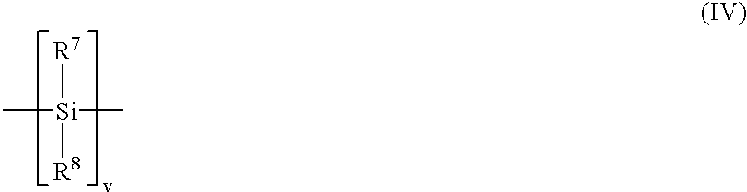
- the non-conjugated spacer group may be a ⁇ -conjugated spacer group, because the ⁇ -conjugated spacer group can connect the electron hole-transporting units maintaining independence of each electron hole-transporting unit.
- Preferred ⁇ -conjugated spacer groups may comprise one or more Si atoms, such as those represented by the following formula (IV):
- v is an integer of 1 or more
- each of R 7 and R 8 independently is an alkyl group having 1 to 30 carbon atoms or an unsubstituted or substituted aryl group having 6 to 30 carbon atoms.
- the substituent may be alkyl or alkoxy of 1-24 carbon atoms.
- each of Ar 1 through Ar 4 independently is a substituted or unsubstituted arylene group having 6 to 30 carbon atoms; each of Ar 5 and Ar 6 independently is an alkyl group having 1 to 30 carbon atoms, or a substituted or unsubstituted aryl group having 6 to 30 carbon atoms.
- the substituent can be alkyl or alkoxy of 1-24 carbon atoms.
- G is a single bond, an alkylene group having 5 to 30 carbon atoms, a cycloalkylene group having 5 to 30 carbon atoms, an arylene group having 6 to 30 carbon atoms, —O—, —S—, or a divalent group represented by the formula (VI) or (VII):
- Ar 7 is an aryl group having 6 to 30 carbon atoms
- Ar 8 is an arylene group having 6 to 30 carbon atoms
- each of Ar 9 and Ar 10 is an aryl group having 6 to 30 carbon atoms.
- the groups for G may have one or more substituents such as those described hereinbefore.
- Two or more divalent units of the formula (V) can be connected by a non-conjugated spacer group such as a group of ester, ether, carbonate, urethane, amide, sulfone, ketone or the aforementioned ⁇ -conjugated spacer group
- polymer of the formula (V) are conjugated carbonate polymers which are represented by the formula (VIII):
- each of Ar 1 through Ar 6 and G has the same meaning as above, each of p and q is 0, 1 or 2, X is a non-conjugated spacer group, and n is 2 or more.
- the most preferable conjugated carbonate polymer is co-poly[3,3′-hydroxytetraphenylbenzidine/diethyleneglycol]carbonate such as that having a number average molecular weight (Mn) of 20,000 and a weight average molecular weight (Mw) of 70,000 which represented by the following formula:
- each of a, b and c is 0 or an integer of 1 to 9, provided that their total number (a+b+c) is 3 or more, and each of R 9 to R 14 independently is a hydrogen atom, or a linear or branched alkyl or alkoxy group having 1 to 15 carbon atoms, provided that at least one of R 9 and R 10 (or R 11 and R 12 , or R 13 and R 14 ) is not a hydrogen atom.
- Two or more divalent units of the formula (IX) can be connected by a non-conjugated spacer group such as ester, ether, carbonate, urethane, amide, sulfone, ketone or the aforementioned ⁇ -conjugated spacer group.
- a non-conjugated spacer group such as ester, ether, carbonate, urethane, amide, sulfone, ketone or the aforementioned ⁇ -conjugated spacer group.
- each of R 15 to R 20 independently is a hydrogen atom, a halogen atom, an alkyl group having 1 to 30 carbon atoms, an aryl group having 6 to 24 carbon atoms, an aralkyl group having 7 to 24 carbon atoms, an aryloxy group having 6 to 24 carbon atoms, an alkylthio group having 1 to 30 carbon atoms, a mono- or di-alkylamino group having alkyl of 1-30 carbon atoms, an arylthio group having 6 to 24 carbon atoms, a mono- or diarylamino group having aryl of 6-24 carbon atoms, a nitro group, or a cyano group d is an integer of 1 to 500.
- Two or more divalent units of the formula (X) can be connected by a non-conjugated spacer group such as a group of ester, ether, carbonate, urethane, amide, sulfone, ketone or the aforementioned ⁇ -conjugated spacer group.
- a non-conjugated spacer group such as a group of ester, ether, carbonate, urethane, amide, sulfone, ketone or the aforementioned ⁇ -conjugated spacer group.
- each of Ar 11 through Ar 14 and Ar 17 through Ar 21 independently is a substituted or unsubstituted arylene group having 6 to 30 carbon atoms; each of Ar 15 , Ar 16 , Ar 22 and Ar23 independently is a substituted or unsubstituted aryl group having 6 to 30 carbon atoms; each of R 21 and R 22 independently is a hydrogen atom, an alkyl group having 1 to 30 carbon atoms, or a substituted or unsubstituted aryl group having 6 to 30 carbon atoms; each of e and f is 0 or 1; and the dotted curve line means the presence of a single bond or an alkylene group of 1-6 carbon atoms to combine the terminal groups
- Two or more divalent units of the formula (XI) or (XII) can be connected by a non-conjugated spacer group such as a group of ester, ether, carbonate, urethane, amide, sulfone, ketone or the aforementioned ⁇ -conjugated spacer group.
- a non-conjugated spacer group such as a group of ester, ether, carbonate, urethane, amide, sulfone, ketone or the aforementioned ⁇ -conjugated spacer group.
- the electron acceptor to be incorporated into the electron hole-transporting layer serves for oxidizing the electron hole-transporting units of the polymer to impart to the polymer increased electroconductivity such as an electroconductivity of 10 ⁇ 10 to 10 3 S ⁇ cm ⁇ 1 .
- the electron accepter is preferably incorporated into the electron hole-transporting layer in an amount of 10 ⁇ 3 to 30 wt. %.
- electron acceptors examples include metal halides, Lewis acids, organic acids, and salts of arylamines and metal halides or Lewis acids.
- metal halides and Lewis acids examples include FeCl 3 , AlCl 3 , SbCl 3 , AsF 5 , and BF 3 .
- A is an acid group such as sulfonic acid group, phosphoric acid group, boric acid group, or carboxylic acid group;
- R is an alkyl, alkoxy or alkylthio group having 1 to 20 carbon atoms, an alkoxlkyl, alkylthioalkyl, or alkenyl group having 2 to 20 carbon atoms, a cycloalkyl group having 5 to 20 carbon atoms, an aryl group having 6 to 20 carbon atoms, an alkaryl or aralkyl group having 7 to 20 carbon atoms, a heterocyclic group such as pyridyl, quinolyl, furanyl, pyrrolyl or thienyl, a halogen atom, a nitro group, a cyano group, or an epoxy group; and m is an integer of 0 to 5].
- the organic acid can be a polymer acid which contains an acid group (such as “A” in the formula (XIII)).
- examples of the polymer acids include sulfonated polystyrene, sulfonated polyethylene, sulfonated polycarbonate, and polyacrylic acid.
- L is a metal halide or a Lewis acid
- X ⁇ is an anion such as a halogen ion
- each of Ar 24 through Ar 26 independently is a substituted or unsubstituted aromatic group having 5 to 30 carbon atoms or a heterocyclic group.
- a preferred electron acceptor represented by the formula (XIV) is tris(4-bromophenyl)ammonium hexachloroantimonate having the following formula:
- the electron acceptors can be employed singly or in combination.
- the thickness of the electron hole-transporting layer of the organic semiconductor laser device of the invention preferably is less than 2,000 nm.
- the light-emitting layer may contain a known fluorescent dye.
- the dye preferably shows a population inversion at a low exciting energy so that the organic dye can produce an emission at an electric current having a low energy (i.e., low electric current density).
- Preferred organic dyes have a laser threshold value such as less than 50 ⁇ J, more preferably less than 1 ⁇ J. Examples of the preferred organic dyes are described below.
- An emission in the ultraviolet or near ultraviolet region can be produced using a para-polyphenylene dye which can be substituted with one or more substituents such as alkoxy, hydroxy, sulfonyl, carboxy, alkoxycarbonyl, amino, dimethylamino or diphenylamino.
- substituents such as alkoxy, hydroxy, sulfonyl, carboxy, alkoxycarbonyl, amino, dimethylamino or diphenylamino.
- Examples of the para-polyphenylene dyes are p-quaterphenyl, 3,5,3′,5′-tetra-t-butyl-p-quinqphenyl, and 3,5,3′,5′-tetra-t-butyl-p-sequisiphenyl.
- a blue or green emission can be produced using a fluorescent brightener belonging to benzothiazole type, benzoimidazole type or benzoxazole type, a metal chelate oxinoide compound, and a styrylbenzene compound.
- Organic dimethylidine compounds described in European Patent No. 388 768 can be employed.
- organic dimethylidine compounds examples include 1,4-phenylenedimethylidine, 4,4′-biphenylenedimethylidine, 2,5-xylylenedimethylidine, 2,6-naphthylinedimethylidine, 1,4-p-terephenylenedimethylidine, 4,4′-bis(2,3-diphenylvinyl)biphenyl (DTBWBi), 4,4′-bis(2,2-dipheylvinyl)biphenyl (DPVBi), and their derivatives.
- Z is a benzene-ring containing-hydrocarbyl group having 6 to 24 carbon atoms; O—Z is a phenolate ligand; Q is a substituted 8-quinolilate ligand; and J is a substituent of the 8-quinolilate ring which disturbs attachment of more than 2 substituted 8-quinolilate ligand to the aluminum atom by steric hindrance].
- Examples of these compounds are bis(2-methyl-8-quinolilate) (p-phenylphenolate)aluminum(III) and bis(2-methyl-8-quinolilate) (1-naphthlate)aluminum(III).
- a mixture of blue or green emissions can be produced using the above-mentioned dye with a dopant, as described in Japanese Patent Provisional Publication H6-9953.
- the dopant may be a dye of blue or green region, such as cumarin or the above-mentioned dye for the blue or green emission
- a preferred combination is a dopant having a diphenylaminovinylarylene skeleton such as 4,4′-[4-(N,N-diphenylamino)styryl]benzene (DPAVB) and a host compound having a distyrylarylene skeleton such as DPVBi.
- Diaminostyrylbenzene (DADSB) having the following formula has a low laser threshold value such as less than 1 ⁇ J, and therefore is favorably used as a light-emitting compound of the organic semiconductor laser of the invention:
- the light-emitting layer generally has a thickness of 5 to 500 nm.
- the electron-transporting layer receives electrons from the negative electrode layer and transmit the received electrons to the light-emitting layer.
- electron-transporting materials which are known for the formation of an organic electroluminescence (EL) device can be employed.
- electron-transporting materials examples include heterocyclic tetracarboxylic anhydrides such as nitro-substituted fluorene derivatives, diphenylquinoline derivatives, thiopyranedioxide derivatives and naphthaleneperylene, carbodiimides, fluorenidenemethane derivatives, anthraquinodimethane and anthrone derivatives, and oxadiazole derivatives.
- heterocyclic tetracarboxylic anhydrides such as nitro-substituted fluorene derivatives, diphenylquinoline derivatives, thiopyranedioxide derivatives and naphthaleneperylene
- carbodiimides fluorenidenemethane derivatives, anthraquinodimethane and anthrone derivatives
- oxadiazole derivatives examples include oxadiazole derivatives.
- thiadiazole derivatives and quinoxaline derivatives having a electron-attracting quinoxaline ring can be employed as the electron-transporting materials.
- metal complexes of the 8-quinolynol derivatives such as tris(8-guinolynol)aluminum (Alq), tris(5,7-dichloro-8-quinolynol)aluminum, tris(5,7-dibromo-8-quinolynol)aluminum, tris(2-methyl-8-quinolynol)aluminum, tris(5-methyl-8-quinolynol)aluminum, and bis(8-quinolynol)zinc can be employed as the electron-transporting materials.
- metal phthalocyanines metal-free phthalocyanines
- metal or metal-free phthalacyanines having a substituent such as an alkyl group or a sulfonic acid group.
- inorganic semiconductor materials such as n-Si and n-SiC.
- the electron-transporting layer preferably contains an electron doner such as an alkali metal, an alkaline earth metal, their fluorides, chlorides, or iodides in an amount of 0.1 to 30 molar %.
- an electron doner such as an alkali metal, an alkaline earth metal, their fluorides, chlorides, or iodides in an amount of 0.1 to 30 molar %.
- the incorporation of the electron doner increases the electron-transporting power so that the thick electron-transporting layer of the organic semiconductor laser device of the invention can smoothly transport electrons to the light-emitting layer.
- the thickness of the electron-transporting layer of the organic semiconductor laser device of the invention preferably is less than 2,000 nm.
- the negative electrode layer supplies electrons to the electron-transporting layer.
- the negative electrode layer is preferably produced using a metal, metal alloy, an electroconductive material or their mixtures to show a low work function such as those less than 4 eV
- the electrode materials are Na, Na/K alloy, Mg, Li, Mg/Cu mixture, Mg/Ag alloy, Al/Li alloy, Al/Al 2 O 3 mixture, In, and rare earth elements.
- the negative electrode layer generally has a thickness of 10 nm to 1 ⁇ m, preferably 50 to 200 nm.
- the organic semiconductor laser device of the invention can be manufactured by the following procedures.
- a positive electrode layer is formed by vapor deposition or sputtering.
- the electron hole-transporting layer, light-emitting layer and electron-transporting layer are formed in order by appropriate methods such as spin-coating, casting, vapor deposition, or sputtering.
- the electron hole-transporting layer is preferably formed by spin-coating, while the light-emitting layer and electron-transporting layer are preferably formed by vapor deposition.
- the conditions of vapor deposition for the formation of the light-emitting layer and electron-transporting layer are variable, but the conditions such as a boat-heating temperature of 50 to 400° C., vacuum of 10 ⁇ 6 to 10 3 Pa, deposition rate of 0.001 to 50 nm/sec, and a substrate temperature of ⁇ 50° C. to 200° C. are preferably employed.
- a negative electrode layer is formed by an appropriate method such as vapor deposition or sputtering.
- a glass plate having an ITO layer of 150 nm thick was washed with oxygen plasma for 30 seconds using a plasma washing means (BPI, available from Samco International Corp.). On thus washed ITC layer, co-poly[3,3′-hydroxytetraphenylbenzidine/diethyleneglycol]carbonate is deposited under vacuum to form an electron hole-transporting layer of 220 nm thick.
- BPI plasma washing means
- the aforementioned diaminostyrylbenzene (DADSB) was deposited under vacuum to form a light-emitting layer of 100 nm.
- an oxadiazole derivative having the following formula was deposited under vacuum to form an electron-transporting layer of 240 nm thick:
- Mg/Ag alloy was deposited under vacuum to form a negative electrode layer of 200 nm.
- an organic semiconductor laser device of the invention having the structure illustrated in FIG. 1 was manufactured.
- the refractive indexes of the functional layers were as follows:
- Electron hole-transporting layer 1.75 Light-emitting layer: 2.11 Electron-transporting layer: 1.93
- Example 2 The procedures of Example 1 were repeated except that the electron hole-transporting layer was prepared by coating a solution of the co-poly[3,3′-hydroxytetraphenylbenzidine/diethyleneglycol]carbonate (50 mg) and the tris(4-bromophenyl)ammonium hexachloroantimonate (5 mg) in 1 mL was spin-coated on the positive electrode layer at 1,000 r.p.m., and heating the coated layer to 80° C. for 1 hour for removing the solvent, to form an electron hole-transporting layer of 650 nm thick
- Example 1 The procedures of Example 1 were repeated except that the electron hole-transporting layer was formed to have a thickness of 50 nm and the electron-transporting layer was formed to have a thickness of 50 nm.
Abstract

Description


| Electron hole-transporting layer: | 1.75 | ||
| Light-emitting layer: | 2.11 | ||
| Electron-transporting layer: | 1.93 | ||
Claims (9)

Applications Claiming Priority (2)
| Application Number | Priority Date | Filing Date | Title |
|---|---|---|---|
| JP26070998 | 1998-09-14 | ||
| JP10-260709 | 1998-09-14 |
Publications (2)
| Publication Number | Publication Date |
|---|---|
| US20030103537A1 US20030103537A1 (en) | 2003-06-05 |
| US6631147B2 true US6631147B2 (en) | 2003-10-07 |
Family
ID=17351683
Family Applications (1)
| Application Number | Title | Priority Date | Filing Date |
|---|---|---|---|
| US09/395,130 Expired - Lifetime US6631147B2 (en) | 1998-09-14 | 1999-09-14 | Organic semiconductor laser device |
Country Status (1)
| Country | Link |
|---|---|
| US (1) | US6631147B2 (en) |
Cited By (13)
| Publication number | Priority date | Publication date | Assignee | Title |
|---|---|---|---|---|
| US20030015668A1 (en) * | 2000-02-09 | 2003-01-23 | Montagu Jean I. | Quantified fluorescence microscopy |
| US20030161368A1 (en) * | 2001-10-12 | 2003-08-28 | Eastman Kodak Company | Organic vertical cavity lasing devices having organic active region |
| US20040207312A1 (en) * | 2003-01-23 | 2004-10-21 | Seiko Epson Corporation | Manufacturing method for organic electroluminescence device, and electronic device therewith |
| US20040213308A1 (en) * | 2003-04-23 | 2004-10-28 | Hiroko Abe | Laser oscillator |
| US20050058162A1 (en) * | 2003-09-12 | 2005-03-17 | Semiconductor Energy Laboratory Co., Ltd. | Laser oscillator |
| US20050056856A1 (en) * | 2003-09-12 | 2005-03-17 | Semiconductor Energy Laboratory Co., Ltd. | Light-emitting device |
| US20050069012A1 (en) * | 2003-09-26 | 2005-03-31 | Semiconductor Energy Laboratory Co., Ltd. | Light emitting device |
| US20050211973A1 (en) * | 2004-03-23 | 2005-09-29 | Kiyotaka Mori | Stressed organic semiconductor |
| US20060049746A1 (en) * | 2003-01-21 | 2006-03-09 | Kyushi Electric Power Co., Inc. | Electroluminescent element |
| US20070272919A1 (en) * | 2006-05-24 | 2007-11-29 | Matsushita Electric Industrial Co., Ltd. | Stressed organic semiconductor devices |
| US20090052491A1 (en) * | 2003-06-27 | 2009-02-26 | Semiconductor Energy Laboratory Co., Ltd. | Organic laser apparatus |
| US20090058274A1 (en) * | 2007-08-17 | 2009-03-05 | Rohm Co., Ltd. | Organic Electroluminescence Device and Organic Laser Diode |
| US20100161266A1 (en) * | 2008-12-19 | 2010-06-24 | Affymetrix, Inc. | System, method and product for calibrating inspection tools |
Families Citing this family (3)
| Publication number | Priority date | Publication date | Assignee | Title |
|---|---|---|---|---|
| US7307940B2 (en) * | 2003-06-30 | 2007-12-11 | Semiconductor Energy Laboratory Co., Ltd. | Optical pick-up device |
| US20050008052A1 (en) * | 2003-07-01 | 2005-01-13 | Ryoji Nomura | Light-emitting device |
| US7242703B2 (en) * | 2004-12-21 | 2007-07-10 | The Trustees Of Princeton University | Organic injection laser |
Citations (3)
| Publication number | Priority date | Publication date | Assignee | Title |
|---|---|---|---|---|
| US5780174A (en) * | 1995-10-27 | 1998-07-14 | Kabushiki Kaisha Toyota Chuo Kenkyusho | Micro-optical resonator type organic electroluminescent device |
| US5998803A (en) * | 1997-05-29 | 1999-12-07 | The Trustees Of Princeton University | Organic light emitting device containing a hole injection enhancement layer |
| US6111902A (en) * | 1997-05-09 | 2000-08-29 | The Trustees Of Princeton University | Organic semiconductor laser |
-
1999
- 1999-09-14 US US09/395,130 patent/US6631147B2/en not_active Expired - Lifetime
Patent Citations (3)
| Publication number | Priority date | Publication date | Assignee | Title |
|---|---|---|---|---|
| US5780174A (en) * | 1995-10-27 | 1998-07-14 | Kabushiki Kaisha Toyota Chuo Kenkyusho | Micro-optical resonator type organic electroluminescent device |
| US6111902A (en) * | 1997-05-09 | 2000-08-29 | The Trustees Of Princeton University | Organic semiconductor laser |
| US5998803A (en) * | 1997-05-29 | 1999-12-07 | The Trustees Of Princeton University | Organic light emitting device containing a hole injection enhancement layer |
Cited By (30)
| Publication number | Priority date | Publication date | Assignee | Title |
|---|---|---|---|---|
| US20030015668A1 (en) * | 2000-02-09 | 2003-01-23 | Montagu Jean I. | Quantified fluorescence microscopy |
| US20070012885A1 (en) * | 2000-02-09 | 2007-01-18 | Affymetrix, Inc. | Quantified fluorescence microscopy |
| US6984828B2 (en) * | 2000-02-09 | 2006-01-10 | Montagu Jean I | Quantified fluorescence microscopy |
| US20050206893A1 (en) * | 2000-02-09 | 2005-09-22 | Affymetrix, Inc. | Quantified fluorescence microscopy |
| US6876684B2 (en) * | 2001-10-12 | 2005-04-05 | Eastman Kodak Company | Organic vertical cavity lasing device having organic active region |
| US20030161368A1 (en) * | 2001-10-12 | 2003-08-28 | Eastman Kodak Company | Organic vertical cavity lasing devices having organic active region |
| US7303825B2 (en) * | 2003-01-21 | 2007-12-04 | Kyushu Electric Power Co., Inc. | Electroluminescence device |
| US20060049746A1 (en) * | 2003-01-21 | 2006-03-09 | Kyushi Electric Power Co., Inc. | Electroluminescent element |
| US20040207312A1 (en) * | 2003-01-23 | 2004-10-21 | Seiko Epson Corporation | Manufacturing method for organic electroluminescence device, and electronic device therewith |
| US7252570B2 (en) * | 2003-01-23 | 2007-08-07 | Seiko Epson Corporation | Manufacturing method for organic electroluminescence device, and electronic device therewith |
| US7505487B2 (en) | 2003-04-23 | 2009-03-17 | Semiconductor Energy Laboratory Co., Ltd. | Laser oscillator including phosphorescent material |
| US20040213308A1 (en) * | 2003-04-23 | 2004-10-28 | Hiroko Abe | Laser oscillator |
| US20090052491A1 (en) * | 2003-06-27 | 2009-02-26 | Semiconductor Energy Laboratory Co., Ltd. | Organic laser apparatus |
| US7449724B2 (en) | 2003-09-12 | 2008-11-11 | Semiconductor Energy Laboratory Co., Ltd. | Light-emitting device |
| US7502392B2 (en) | 2003-09-12 | 2009-03-10 | Semiconductor Energy Laboratory Co., Ltd. | Laser oscillator |
| US20050058162A1 (en) * | 2003-09-12 | 2005-03-17 | Semiconductor Energy Laboratory Co., Ltd. | Laser oscillator |
| US8867585B2 (en) | 2003-09-12 | 2014-10-21 | Semiconductor Energy Laboratory Co., Ltd. | Laser oscillator |
| US8059692B2 (en) | 2003-09-12 | 2011-11-15 | Semiconductor Energy Labortory Co., Ltd. | Laser oscillator |
| US20090185584A1 (en) * | 2003-09-12 | 2009-07-23 | Semiconductor Energy Laboratory Co., Ltd. | Laser oscillator |
| US20050056856A1 (en) * | 2003-09-12 | 2005-03-17 | Semiconductor Energy Laboratory Co., Ltd. | Light-emitting device |
| US20050069012A1 (en) * | 2003-09-26 | 2005-03-31 | Semiconductor Energy Laboratory Co., Ltd. | Light emitting device |
| US7260135B2 (en) | 2003-09-26 | 2007-08-21 | Semiconductor Energy Laboratory Co., Ltd. | Light emitting device |
| US20060208255A1 (en) * | 2004-03-23 | 2006-09-21 | Klyotaka Mori | Stressed organic semiconductor |
| US20050211973A1 (en) * | 2004-03-23 | 2005-09-29 | Kiyotaka Mori | Stressed organic semiconductor |
| US20060214163A1 (en) * | 2004-03-23 | 2006-09-28 | Kiyotaka Mori | Stressed organic semiconductor |
| US20070272919A1 (en) * | 2006-05-24 | 2007-11-29 | Matsushita Electric Industrial Co., Ltd. | Stressed organic semiconductor devices |
| US20090058274A1 (en) * | 2007-08-17 | 2009-03-05 | Rohm Co., Ltd. | Organic Electroluminescence Device and Organic Laser Diode |
| US7965037B2 (en) * | 2007-08-17 | 2011-06-21 | Kyushu University, National University Corporation | Organic electroluminescence device and organic laser diode |
| US20100161266A1 (en) * | 2008-12-19 | 2010-06-24 | Affymetrix, Inc. | System, method and product for calibrating inspection tools |
| US8374818B2 (en) | 2008-12-19 | 2013-02-12 | Affymetrix, Inc. | System, method and apparatus for calibrating inspection tools |
Also Published As
| Publication number | Publication date |
|---|---|
| US20030103537A1 (en) | 2003-06-05 |
Similar Documents
| Publication | Publication Date | Title |
|---|---|---|
| US6631147B2 (en) | Organic semiconductor laser device | |
| US10998527B2 (en) | Organic electroluminescent device | |
| US6831406B1 (en) | Electroluminescent device having a very thin emission layer | |
| Kido et al. | Bright red light‐emitting organic electroluminescent devices having a europium complex as an emitter | |
| US7309619B2 (en) | Light-emitting element, production method thereof, and light-emitting apparatus | |
| US9203046B2 (en) | Organic electroluminescent device and production process thereof | |
| US6125226A (en) | Light emitting devices having high brightness | |
| JP4611578B2 (en) | Organic electroluminescent device | |
| US8415875B2 (en) | Light emissive device having cathode comprising a codeposited mixed layer | |
| US7965037B2 (en) | Organic electroluminescence device and organic laser diode | |
| JP2991183B2 (en) | Organic electroluminescence device | |
| US6558817B1 (en) | Organic electroluminescent element | |
| US6210814B1 (en) | Color-tunable organic light emitting devices | |
| US7118810B2 (en) | Organic/polymer electroluminescent devices employing single-ion conductors | |
| US6287712B1 (en) | Color-tunable organic light emitting devices | |
| US7411223B2 (en) | Compound electrodes for electronic devices | |
| JP3640578B2 (en) | Organic semiconductor laser | |
| Kido et al. | Molecularly doped polymers for organic electroluminescent devices | |
| US7522644B2 (en) | Laser oscillator | |
| JP2004146067A (en) | Organic light emitting device | |
| JP2001196178A (en) | Luminous element | |
| JP2002015874A (en) | Organic luminescent element | |
| Kippelen et al. | Electroluminescence in an organic polymer channel waveguide |
Legal Events
| Date | Code | Title | Description |
|---|---|---|---|
| AS | Assignment |
Owner name: OPTC CO., LTD, JAPAN Free format text: ASSIGNMENT OF ASSIGNORS INTEREST;ASSIGNORS:TANIGUCHI, YOSHIO;ADACHI, CHIHAYA;KOYAMA, TOSHIKI;AND OTHERS;REEL/FRAME:010256/0297 Effective date: 19990908 |
|
| STCF | Information on status: patent grant |
Free format text: PATENTED CASE |
|
| AS | Assignment |
Owner name: MIRAIAL CO., LTD., JAPAN Free format text: ASSIGNMENT OF ASSIGNORS INTEREST;ASSIGNOR:OPTC CO., LTD;REEL/FRAME:018039/0472 Effective date: 20050825 |
|
| FEPP | Fee payment procedure |
Free format text: PAT HOLDER CLAIMS SMALL ENTITY STATUS, ENTITY STATUS SET TO SMALL (ORIGINAL EVENT CODE: LTOS); ENTITY STATUS OF PATENT OWNER: SMALL ENTITY |
|
| FPAY | Fee payment |
Year of fee payment: 4 |
|
| FPAY | Fee payment |
Year of fee payment: 8 |
|
| AS | Assignment |
Owner name: KYUSHU UNIVERSITY, NATIONAL UNIVERSITY CORPORATION Free format text: ASSIGNMENT OF ASSIGNORS INTEREST;ASSIGNOR:ADACHI, CHIHAYA;REEL/FRAME:026095/0530 Effective date: 20110124 Owner name: ADACHI, CHIHAYA, JAPAN Free format text: ASSIGNMENT OF ASSIGNORS INTEREST;ASSIGNOR:MIRAIAL CO., LTD;REEL/FRAME:026095/0506 Effective date: 20110124 |
|
| FPAY | Fee payment |
Year of fee payment: 12 |