US6608654B2 - Methods of fabricating active matrix pixel electrodes - Google Patents
Methods of fabricating active matrix pixel electrodes Download PDFInfo
- Publication number
- US6608654B2 US6608654B2 US08/716,409 US71640997A US6608654B2 US 6608654 B2 US6608654 B2 US 6608654B2 US 71640997 A US71640997 A US 71640997A US 6608654 B2 US6608654 B2 US 6608654B2
- Authority
- US
- United States
- Prior art keywords
- active matrix
- liquid crystal
- pixel electrodes
- transistor
- pixel electrode
- Prior art date
- Legal status (The legal status is an assumption and is not a legal conclusion. Google has not performed a legal analysis and makes no representation as to the accuracy of the status listed.)
- Expired - Fee Related
Links
- 239000011159 matrix material Substances 0.000 title claims abstract description 40
- 238000000034 method Methods 0.000 title abstract description 47
- 239000000758 substrate Substances 0.000 claims abstract description 29
- 239000010409 thin film Substances 0.000 claims abstract description 15
- 239000010410 layer Substances 0.000 claims description 62
- 239000000463 material Substances 0.000 claims description 28
- 239000004973 liquid crystal related substance Substances 0.000 claims description 24
- 229910021421 monocrystalline silicon Inorganic materials 0.000 claims description 17
- 239000000853 adhesive Substances 0.000 claims description 12
- 230000001070 adhesive effect Effects 0.000 claims description 12
- 229920001721 polyimide Polymers 0.000 claims description 11
- VYPSYNLAJGMNEJ-UHFFFAOYSA-N Silicium dioxide Chemical compound O=[Si]=O VYPSYNLAJGMNEJ-UHFFFAOYSA-N 0.000 claims description 7
- 239000004065 semiconductor Substances 0.000 claims description 7
- 150000004767 nitrides Chemical class 0.000 claims description 6
- 229910052751 metal Inorganic materials 0.000 claims description 5
- 239000002184 metal Substances 0.000 claims description 5
- 229910044991 metal oxide Inorganic materials 0.000 claims description 5
- 150000004706 metal oxides Chemical class 0.000 claims description 5
- 239000002210 silicon-based material Substances 0.000 claims description 4
- AMGQUBHHOARCQH-UHFFFAOYSA-N indium;oxotin Chemical compound [In].[Sn]=O AMGQUBHHOARCQH-UHFFFAOYSA-N 0.000 claims description 3
- 239000000377 silicon dioxide Substances 0.000 claims description 3
- 229910021420 polycrystalline silicon Inorganic materials 0.000 claims description 2
- 235000012239 silicon dioxide Nutrition 0.000 claims description 2
- 229920005591 polysilicon Polymers 0.000 claims 1
- 238000012546 transfer Methods 0.000 abstract description 20
- XUIMIQQOPSSXEZ-UHFFFAOYSA-N Silicon Chemical compound [Si] XUIMIQQOPSSXEZ-UHFFFAOYSA-N 0.000 abstract description 18
- 229910052710 silicon Inorganic materials 0.000 abstract description 18
- 239000010703 silicon Substances 0.000 abstract description 18
- 230000015572 biosynthetic process Effects 0.000 abstract description 7
- 238000003491 array Methods 0.000 abstract 1
- 230000008569 process Effects 0.000 description 32
- 238000004519 manufacturing process Methods 0.000 description 18
- 239000007772 electrode material Substances 0.000 description 12
- 239000012212 insulator Substances 0.000 description 12
- 238000001465 metallisation Methods 0.000 description 11
- 239000004642 Polyimide Substances 0.000 description 10
- 239000000839 emulsion Substances 0.000 description 10
- 229910052709 silver Inorganic materials 0.000 description 9
- 239000004332 silver Substances 0.000 description 9
- 229920002120 photoresistant polymer Polymers 0.000 description 8
- 238000012545 processing Methods 0.000 description 8
- GWEVSGVZZGPLCZ-UHFFFAOYSA-N Titan oxide Chemical compound O=[Ti]=O GWEVSGVZZGPLCZ-UHFFFAOYSA-N 0.000 description 7
- 238000002161 passivation Methods 0.000 description 7
- -1 altiminium nitride Chemical class 0.000 description 6
- 230000005540 biological transmission Effects 0.000 description 6
- 239000011521 glass Substances 0.000 description 6
- 238000002955 isolation Methods 0.000 description 6
- 229910021417 amorphous silicon Inorganic materials 0.000 description 5
- 238000000151 deposition Methods 0.000 description 5
- 230000008021 deposition Effects 0.000 description 5
- 239000010408 film Substances 0.000 description 5
- 235000012431 wafers Nutrition 0.000 description 5
- PXHVJJICTQNCMI-UHFFFAOYSA-N Nickel Chemical compound [Ni] PXHVJJICTQNCMI-UHFFFAOYSA-N 0.000 description 4
- BQCADISMDOOEFD-UHFFFAOYSA-N Silver Chemical compound [Ag] BQCADISMDOOEFD-UHFFFAOYSA-N 0.000 description 4
- XLOMVQKBTHCTTD-UHFFFAOYSA-N Zinc monoxide Chemical compound [Zn]=O XLOMVQKBTHCTTD-UHFFFAOYSA-N 0.000 description 4
- 238000013459 approach Methods 0.000 description 4
- 230000008901 benefit Effects 0.000 description 4
- 238000004061 bleaching Methods 0.000 description 3
- 239000000945 filler Substances 0.000 description 3
- 239000002904 solvent Substances 0.000 description 3
- 239000004408 titanium dioxide Substances 0.000 description 3
- IJGRMHOSHXDMSA-UHFFFAOYSA-N Atomic nitrogen Chemical compound N#N IJGRMHOSHXDMSA-UHFFFAOYSA-N 0.000 description 2
- KDLHZDBZIXYQEI-UHFFFAOYSA-N Palladium Chemical compound [Pd] KDLHZDBZIXYQEI-UHFFFAOYSA-N 0.000 description 2
- 239000002318 adhesion promoter Substances 0.000 description 2
- 239000004020 conductor Substances 0.000 description 2
- 238000011161 development Methods 0.000 description 2
- 229910052759 nickel Inorganic materials 0.000 description 2
- 230000003287 optical effect Effects 0.000 description 2
- 229920003023 plastic Polymers 0.000 description 2
- 230000010287 polarization Effects 0.000 description 2
- 238000004381 surface treatment Methods 0.000 description 2
- 239000011787 zinc oxide Substances 0.000 description 2
- OKTJSMMVPCPJKN-UHFFFAOYSA-N Carbon Chemical compound [C] OKTJSMMVPCPJKN-UHFFFAOYSA-N 0.000 description 1
- OAICVXFJPJFONN-UHFFFAOYSA-N Phosphorus Chemical compound [P] OAICVXFJPJFONN-UHFFFAOYSA-N 0.000 description 1
- 229910052581 Si3N4 Inorganic materials 0.000 description 1
- 241000376353 Stips Species 0.000 description 1
- 238000010521 absorption reaction Methods 0.000 description 1
- 239000012790 adhesive layer Substances 0.000 description 1
- 230000004075 alteration Effects 0.000 description 1
- QVGXLLKOCUKJST-UHFFFAOYSA-N atomic oxygen Chemical compound [O] QVGXLLKOCUKJST-UHFFFAOYSA-N 0.000 description 1
- 229910052799 carbon Inorganic materials 0.000 description 1
- 238000005229 chemical vapour deposition Methods 0.000 description 1
- 229910052681 coesite Inorganic materials 0.000 description 1
- 239000003086 colorant Substances 0.000 description 1
- 239000002131 composite material Substances 0.000 description 1
- 230000002596 correlated effect Effects 0.000 description 1
- 230000000875 corresponding effect Effects 0.000 description 1
- 229910052906 cristobalite Inorganic materials 0.000 description 1
- 239000013078 crystal Substances 0.000 description 1
- 230000000694 effects Effects 0.000 description 1
- 230000005684 electric field Effects 0.000 description 1
- 230000008030 elimination Effects 0.000 description 1
- 238000003379 elimination reaction Methods 0.000 description 1
- 238000005538 encapsulation Methods 0.000 description 1
- 238000005530 etching Methods 0.000 description 1
- 239000012530 fluid Substances 0.000 description 1
- 238000002513 implantation Methods 0.000 description 1
- 238000010348 incorporation Methods 0.000 description 1
- 230000031700 light absorption Effects 0.000 description 1
- 230000000873 masking effect Effects 0.000 description 1
- 229910021645 metal ion Inorganic materials 0.000 description 1
- 229910052757 nitrogen Inorganic materials 0.000 description 1
- 229910052760 oxygen Inorganic materials 0.000 description 1
- 239000001301 oxygen Substances 0.000 description 1
- 229910052763 palladium Inorganic materials 0.000 description 1
- 239000002245 particle Substances 0.000 description 1
- 238000000059 patterning Methods 0.000 description 1
- 238000000206 photolithography Methods 0.000 description 1
- 239000000049 pigment Substances 0.000 description 1
- 239000004033 plastic Substances 0.000 description 1
- CLSUSRZJUQMOHH-UHFFFAOYSA-L platinum dichloride Chemical compound Cl[Pt]Cl CLSUSRZJUQMOHH-UHFFFAOYSA-L 0.000 description 1
- 238000003672 processing method Methods 0.000 description 1
- 238000001953 recrystallisation Methods 0.000 description 1
- 230000009467 reduction Effects 0.000 description 1
- 230000004044 response Effects 0.000 description 1
- 238000000926 separation method Methods 0.000 description 1
- 150000003376 silicon Chemical class 0.000 description 1
- HQVNEWCFYHHQES-UHFFFAOYSA-N silicon nitride Chemical compound N12[Si]34N5[Si]62N3[Si]51N64 HQVNEWCFYHHQES-UHFFFAOYSA-N 0.000 description 1
- 229910052814 silicon oxide Inorganic materials 0.000 description 1
- 239000007787 solid Substances 0.000 description 1
- 229910052682 stishovite Inorganic materials 0.000 description 1
- XOLBLPGZBRYERU-UHFFFAOYSA-N tin dioxide Chemical compound O=[Sn]=O XOLBLPGZBRYERU-UHFFFAOYSA-N 0.000 description 1
- 229910001887 tin oxide Inorganic materials 0.000 description 1
- OGIDPMRJRNCKJF-UHFFFAOYSA-N titanium oxide Inorganic materials [Ti]=O OGIDPMRJRNCKJF-UHFFFAOYSA-N 0.000 description 1
- 229910052905 tridymite Inorganic materials 0.000 description 1
- WFKWXMTUELFFGS-UHFFFAOYSA-N tungsten Chemical compound [W] WFKWXMTUELFFGS-UHFFFAOYSA-N 0.000 description 1
- 229910052721 tungsten Inorganic materials 0.000 description 1
- 239000010937 tungsten Substances 0.000 description 1
- XLYOFNOQVPJJNP-UHFFFAOYSA-N water Substances O XLYOFNOQVPJJNP-UHFFFAOYSA-N 0.000 description 1
- 239000001052 yellow pigment Substances 0.000 description 1
Images


Classifications
-
- H—ELECTRICITY
- H01—ELECTRIC ELEMENTS
- H01L—SEMICONDUCTOR DEVICES NOT COVERED BY CLASS H10
- H01L27/00—Devices consisting of a plurality of semiconductor or other solid-state components formed in or on a common substrate
- H01L27/02—Devices consisting of a plurality of semiconductor or other solid-state components formed in or on a common substrate including semiconductor components specially adapted for rectifying, oscillating, amplifying or switching and having at least one potential-jump barrier or surface barrier; including integrated passive circuit elements with at least one potential-jump barrier or surface barrier
- H01L27/12—Devices consisting of a plurality of semiconductor or other solid-state components formed in or on a common substrate including semiconductor components specially adapted for rectifying, oscillating, amplifying or switching and having at least one potential-jump barrier or surface barrier; including integrated passive circuit elements with at least one potential-jump barrier or surface barrier the substrate being other than a semiconductor body, e.g. an insulating body
- H01L27/1214—Devices consisting of a plurality of semiconductor or other solid-state components formed in or on a common substrate including semiconductor components specially adapted for rectifying, oscillating, amplifying or switching and having at least one potential-jump barrier or surface barrier; including integrated passive circuit elements with at least one potential-jump barrier or surface barrier the substrate being other than a semiconductor body, e.g. an insulating body comprising a plurality of TFTs formed on a non-semiconducting substrate, e.g. driving circuits for AMLCDs
- H01L27/1259—Multistep manufacturing methods
- H01L27/1262—Multistep manufacturing methods with a particular formation, treatment or coating of the substrate
- H01L27/1266—Multistep manufacturing methods with a particular formation, treatment or coating of the substrate the substrate on which the devices are formed not being the final device substrate, e.g. using a temporary substrate
-
- G—PHYSICS
- G02—OPTICS
- G02B—OPTICAL ELEMENTS, SYSTEMS OR APPARATUS
- G02B27/00—Optical systems or apparatus not provided for by any of the groups G02B1/00 - G02B26/00, G02B30/00
- G02B27/0093—Optical systems or apparatus not provided for by any of the groups G02B1/00 - G02B26/00, G02B30/00 with means for monitoring data relating to the user, e.g. head-tracking, eye-tracking
-
- G—PHYSICS
- G02—OPTICS
- G02F—OPTICAL DEVICES OR ARRANGEMENTS FOR THE CONTROL OF LIGHT BY MODIFICATION OF THE OPTICAL PROPERTIES OF THE MEDIA OF THE ELEMENTS INVOLVED THEREIN; NON-LINEAR OPTICS; FREQUENCY-CHANGING OF LIGHT; OPTICAL LOGIC ELEMENTS; OPTICAL ANALOGUE/DIGITAL CONVERTERS
- G02F1/00—Devices or arrangements for the control of the intensity, colour, phase, polarisation or direction of light arriving from an independent light source, e.g. switching, gating or modulating; Non-linear optics
- G02F1/01—Devices or arrangements for the control of the intensity, colour, phase, polarisation or direction of light arriving from an independent light source, e.g. switching, gating or modulating; Non-linear optics for the control of the intensity, phase, polarisation or colour
- G02F1/13—Devices or arrangements for the control of the intensity, colour, phase, polarisation or direction of light arriving from an independent light source, e.g. switching, gating or modulating; Non-linear optics for the control of the intensity, phase, polarisation or colour based on liquid crystals, e.g. single liquid crystal display cells
- G02F1/133—Constructional arrangements; Operation of liquid crystal cells; Circuit arrangements
- G02F1/1333—Constructional arrangements; Manufacturing methods
- G02F1/1335—Structural association of cells with optical devices, e.g. polarisers or reflectors
- G02F1/133526—Lenses, e.g. microlenses or Fresnel lenses
-
- G—PHYSICS
- G02—OPTICS
- G02F—OPTICAL DEVICES OR ARRANGEMENTS FOR THE CONTROL OF LIGHT BY MODIFICATION OF THE OPTICAL PROPERTIES OF THE MEDIA OF THE ELEMENTS INVOLVED THEREIN; NON-LINEAR OPTICS; FREQUENCY-CHANGING OF LIGHT; OPTICAL LOGIC ELEMENTS; OPTICAL ANALOGUE/DIGITAL CONVERTERS
- G02F1/00—Devices or arrangements for the control of the intensity, colour, phase, polarisation or direction of light arriving from an independent light source, e.g. switching, gating or modulating; Non-linear optics
- G02F1/01—Devices or arrangements for the control of the intensity, colour, phase, polarisation or direction of light arriving from an independent light source, e.g. switching, gating or modulating; Non-linear optics for the control of the intensity, phase, polarisation or colour
- G02F1/13—Devices or arrangements for the control of the intensity, colour, phase, polarisation or direction of light arriving from an independent light source, e.g. switching, gating or modulating; Non-linear optics for the control of the intensity, phase, polarisation or colour based on liquid crystals, e.g. single liquid crystal display cells
- G02F1/133—Constructional arrangements; Operation of liquid crystal cells; Circuit arrangements
- G02F1/1333—Constructional arrangements; Manufacturing methods
- G02F1/1345—Conductors connecting electrodes to cell terminals
- G02F1/13454—Drivers integrated on the active matrix substrate
-
- G—PHYSICS
- G02—OPTICS
- G02F—OPTICAL DEVICES OR ARRANGEMENTS FOR THE CONTROL OF LIGHT BY MODIFICATION OF THE OPTICAL PROPERTIES OF THE MEDIA OF THE ELEMENTS INVOLVED THEREIN; NON-LINEAR OPTICS; FREQUENCY-CHANGING OF LIGHT; OPTICAL LOGIC ELEMENTS; OPTICAL ANALOGUE/DIGITAL CONVERTERS
- G02F1/00—Devices or arrangements for the control of the intensity, colour, phase, polarisation or direction of light arriving from an independent light source, e.g. switching, gating or modulating; Non-linear optics
- G02F1/01—Devices or arrangements for the control of the intensity, colour, phase, polarisation or direction of light arriving from an independent light source, e.g. switching, gating or modulating; Non-linear optics for the control of the intensity, phase, polarisation or colour
- G02F1/13—Devices or arrangements for the control of the intensity, colour, phase, polarisation or direction of light arriving from an independent light source, e.g. switching, gating or modulating; Non-linear optics for the control of the intensity, phase, polarisation or colour based on liquid crystals, e.g. single liquid crystal display cells
- G02F1/133—Constructional arrangements; Operation of liquid crystal cells; Circuit arrangements
- G02F1/136—Liquid crystal cells structurally associated with a semi-conducting layer or substrate, e.g. cells forming part of an integrated circuit
- G02F1/1362—Active matrix addressed cells
- G02F1/136277—Active matrix addressed cells formed on a semiconductor substrate, e.g. of silicon
-
- G—PHYSICS
- G02—OPTICS
- G02F—OPTICAL DEVICES OR ARRANGEMENTS FOR THE CONTROL OF LIGHT BY MODIFICATION OF THE OPTICAL PROPERTIES OF THE MEDIA OF THE ELEMENTS INVOLVED THEREIN; NON-LINEAR OPTICS; FREQUENCY-CHANGING OF LIGHT; OPTICAL LOGIC ELEMENTS; OPTICAL ANALOGUE/DIGITAL CONVERTERS
- G02F1/00—Devices or arrangements for the control of the intensity, colour, phase, polarisation or direction of light arriving from an independent light source, e.g. switching, gating or modulating; Non-linear optics
- G02F1/01—Devices or arrangements for the control of the intensity, colour, phase, polarisation or direction of light arriving from an independent light source, e.g. switching, gating or modulating; Non-linear optics for the control of the intensity, phase, polarisation or colour
- G02F1/13—Devices or arrangements for the control of the intensity, colour, phase, polarisation or direction of light arriving from an independent light source, e.g. switching, gating or modulating; Non-linear optics for the control of the intensity, phase, polarisation or colour based on liquid crystals, e.g. single liquid crystal display cells
- G02F1/133—Constructional arrangements; Operation of liquid crystal cells; Circuit arrangements
- G02F1/136—Liquid crystal cells structurally associated with a semi-conducting layer or substrate, e.g. cells forming part of an integrated circuit
- G02F1/1362—Active matrix addressed cells
- G02F1/1368—Active matrix addressed cells in which the switching element is a three-electrode device
-
- G—PHYSICS
- G09—EDUCATION; CRYPTOGRAPHY; DISPLAY; ADVERTISING; SEALS
- G09G—ARRANGEMENTS OR CIRCUITS FOR CONTROL OF INDICATING DEVICES USING STATIC MEANS TO PRESENT VARIABLE INFORMATION
- G09G3/00—Control arrangements or circuits, of interest only in connection with visual indicators other than cathode-ray tubes
- G09G3/20—Control arrangements or circuits, of interest only in connection with visual indicators other than cathode-ray tubes for presentation of an assembly of a number of characters, e.g. a page, by composing the assembly by combination of individual elements arranged in a matrix no fixed position being assigned to or needed to be assigned to the individual characters or partial characters
- G09G3/22—Control arrangements or circuits, of interest only in connection with visual indicators other than cathode-ray tubes for presentation of an assembly of a number of characters, e.g. a page, by composing the assembly by combination of individual elements arranged in a matrix no fixed position being assigned to or needed to be assigned to the individual characters or partial characters using controlled light sources
- G09G3/30—Control arrangements or circuits, of interest only in connection with visual indicators other than cathode-ray tubes for presentation of an assembly of a number of characters, e.g. a page, by composing the assembly by combination of individual elements arranged in a matrix no fixed position being assigned to or needed to be assigned to the individual characters or partial characters using controlled light sources using electroluminescent panels
-
- G—PHYSICS
- G09—EDUCATION; CRYPTOGRAPHY; DISPLAY; ADVERTISING; SEALS
- G09G—ARRANGEMENTS OR CIRCUITS FOR CONTROL OF INDICATING DEVICES USING STATIC MEANS TO PRESENT VARIABLE INFORMATION
- G09G3/00—Control arrangements or circuits, of interest only in connection with visual indicators other than cathode-ray tubes
- G09G3/20—Control arrangements or circuits, of interest only in connection with visual indicators other than cathode-ray tubes for presentation of an assembly of a number of characters, e.g. a page, by composing the assembly by combination of individual elements arranged in a matrix no fixed position being assigned to or needed to be assigned to the individual characters or partial characters
- G09G3/34—Control arrangements or circuits, of interest only in connection with visual indicators other than cathode-ray tubes for presentation of an assembly of a number of characters, e.g. a page, by composing the assembly by combination of individual elements arranged in a matrix no fixed position being assigned to or needed to be assigned to the individual characters or partial characters by control of light from an independent source
- G09G3/36—Control arrangements or circuits, of interest only in connection with visual indicators other than cathode-ray tubes for presentation of an assembly of a number of characters, e.g. a page, by composing the assembly by combination of individual elements arranged in a matrix no fixed position being assigned to or needed to be assigned to the individual characters or partial characters by control of light from an independent source using liquid crystals
-
- H—ELECTRICITY
- H01—ELECTRIC ELEMENTS
- H01L—SEMICONDUCTOR DEVICES NOT COVERED BY CLASS H10
- H01L27/00—Devices consisting of a plurality of semiconductor or other solid-state components formed in or on a common substrate
- H01L27/02—Devices consisting of a plurality of semiconductor or other solid-state components formed in or on a common substrate including semiconductor components specially adapted for rectifying, oscillating, amplifying or switching and having at least one potential-jump barrier or surface barrier; including integrated passive circuit elements with at least one potential-jump barrier or surface barrier
- H01L27/12—Devices consisting of a plurality of semiconductor or other solid-state components formed in or on a common substrate including semiconductor components specially adapted for rectifying, oscillating, amplifying or switching and having at least one potential-jump barrier or surface barrier; including integrated passive circuit elements with at least one potential-jump barrier or surface barrier the substrate being other than a semiconductor body, e.g. an insulating body
- H01L27/1214—Devices consisting of a plurality of semiconductor or other solid-state components formed in or on a common substrate including semiconductor components specially adapted for rectifying, oscillating, amplifying or switching and having at least one potential-jump barrier or surface barrier; including integrated passive circuit elements with at least one potential-jump barrier or surface barrier the substrate being other than a semiconductor body, e.g. an insulating body comprising a plurality of TFTs formed on a non-semiconducting substrate, e.g. driving circuits for AMLCDs
-
- H—ELECTRICITY
- H01—ELECTRIC ELEMENTS
- H01L—SEMICONDUCTOR DEVICES NOT COVERED BY CLASS H10
- H01L29/00—Semiconductor devices adapted for rectifying, amplifying, oscillating or switching, or capacitors or resistors with at least one potential-jump barrier or surface barrier, e.g. PN junction depletion layer or carrier concentration layer; Details of semiconductor bodies or of electrodes thereof ; Multistep manufacturing processes therefor
- H01L29/66—Types of semiconductor device ; Multistep manufacturing processes therefor
- H01L29/68—Types of semiconductor device ; Multistep manufacturing processes therefor controllable by only the electric current supplied, or only the electric potential applied, to an electrode which does not carry the current to be rectified, amplified or switched
- H01L29/76—Unipolar devices, e.g. field effect transistors
- H01L29/772—Field effect transistors
- H01L29/78—Field effect transistors with field effect produced by an insulated gate
- H01L29/786—Thin film transistors, i.e. transistors with a channel being at least partly a thin film
- H01L29/78606—Thin film transistors, i.e. transistors with a channel being at least partly a thin film with supplementary region or layer in the thin film or in the insulated bulk substrate supporting it for controlling or increasing the safety of the device
- H01L29/78633—Thin film transistors, i.e. transistors with a channel being at least partly a thin film with supplementary region or layer in the thin film or in the insulated bulk substrate supporting it for controlling or increasing the safety of the device with a light shield
-
- H—ELECTRICITY
- H04—ELECTRIC COMMUNICATION TECHNIQUE
- H04N—PICTORIAL COMMUNICATION, e.g. TELEVISION
- H04N5/00—Details of television systems
- H04N5/74—Projection arrangements for image reproduction, e.g. using eidophor
- H04N5/7416—Projection arrangements for image reproduction, e.g. using eidophor involving the use of a spatial light modulator, e.g. a light valve, controlled by a video signal
- H04N5/7441—Projection arrangements for image reproduction, e.g. using eidophor involving the use of a spatial light modulator, e.g. a light valve, controlled by a video signal the modulator being an array of liquid crystal cells
-
- H—ELECTRICITY
- H04—ELECTRIC COMMUNICATION TECHNIQUE
- H04N—PICTORIAL COMMUNICATION, e.g. TELEVISION
- H04N9/00—Details of colour television systems
- H04N9/12—Picture reproducers
- H04N9/31—Projection devices for colour picture display, e.g. using electronic spatial light modulators [ESLM]
- H04N9/3141—Constructional details thereof
-
- G—PHYSICS
- G02—OPTICS
- G02F—OPTICAL DEVICES OR ARRANGEMENTS FOR THE CONTROL OF LIGHT BY MODIFICATION OF THE OPTICAL PROPERTIES OF THE MEDIA OF THE ELEMENTS INVOLVED THEREIN; NON-LINEAR OPTICS; FREQUENCY-CHANGING OF LIGHT; OPTICAL LOGIC ELEMENTS; OPTICAL ANALOGUE/DIGITAL CONVERTERS
- G02F1/00—Devices or arrangements for the control of the intensity, colour, phase, polarisation or direction of light arriving from an independent light source, e.g. switching, gating or modulating; Non-linear optics
- G02F1/01—Devices or arrangements for the control of the intensity, colour, phase, polarisation or direction of light arriving from an independent light source, e.g. switching, gating or modulating; Non-linear optics for the control of the intensity, phase, polarisation or colour
- G02F1/13—Devices or arrangements for the control of the intensity, colour, phase, polarisation or direction of light arriving from an independent light source, e.g. switching, gating or modulating; Non-linear optics for the control of the intensity, phase, polarisation or colour based on liquid crystals, e.g. single liquid crystal display cells
- G02F1/133—Constructional arrangements; Operation of liquid crystal cells; Circuit arrangements
- G02F1/1333—Constructional arrangements; Manufacturing methods
- G02F1/1335—Structural association of cells with optical devices, e.g. polarisers or reflectors
- G02F1/133509—Filters, e.g. light shielding masks
- G02F1/133514—Colour filters
- G02F1/133516—Methods for their manufacture, e.g. printing, electro-deposition or photolithography
-
- G—PHYSICS
- G02—OPTICS
- G02F—OPTICAL DEVICES OR ARRANGEMENTS FOR THE CONTROL OF LIGHT BY MODIFICATION OF THE OPTICAL PROPERTIES OF THE MEDIA OF THE ELEMENTS INVOLVED THEREIN; NON-LINEAR OPTICS; FREQUENCY-CHANGING OF LIGHT; OPTICAL LOGIC ELEMENTS; OPTICAL ANALOGUE/DIGITAL CONVERTERS
- G02F1/00—Devices or arrangements for the control of the intensity, colour, phase, polarisation or direction of light arriving from an independent light source, e.g. switching, gating or modulating; Non-linear optics
- G02F1/01—Devices or arrangements for the control of the intensity, colour, phase, polarisation or direction of light arriving from an independent light source, e.g. switching, gating or modulating; Non-linear optics for the control of the intensity, phase, polarisation or colour
- G02F1/13—Devices or arrangements for the control of the intensity, colour, phase, polarisation or direction of light arriving from an independent light source, e.g. switching, gating or modulating; Non-linear optics for the control of the intensity, phase, polarisation or colour based on liquid crystals, e.g. single liquid crystal display cells
- G02F1/133—Constructional arrangements; Operation of liquid crystal cells; Circuit arrangements
- G02F1/1333—Constructional arrangements; Manufacturing methods
- G02F1/1347—Arrangement of liquid crystal layers or cells in which the final condition of one light beam is achieved by the addition of the effects of two or more layers or cells
- G02F1/13471—Arrangement of liquid crystal layers or cells in which the final condition of one light beam is achieved by the addition of the effects of two or more layers or cells in which all the liquid crystal cells or layers remain transparent, e.g. FLC, ECB, DAP, HAN, TN, STN, SBE-LC cells
- G02F1/13473—Arrangement of liquid crystal layers or cells in which the final condition of one light beam is achieved by the addition of the effects of two or more layers or cells in which all the liquid crystal cells or layers remain transparent, e.g. FLC, ECB, DAP, HAN, TN, STN, SBE-LC cells for wavelength filtering or for colour display without the use of colour mosaic filters
-
- G—PHYSICS
- G02—OPTICS
- G02F—OPTICAL DEVICES OR ARRANGEMENTS FOR THE CONTROL OF LIGHT BY MODIFICATION OF THE OPTICAL PROPERTIES OF THE MEDIA OF THE ELEMENTS INVOLVED THEREIN; NON-LINEAR OPTICS; FREQUENCY-CHANGING OF LIGHT; OPTICAL LOGIC ELEMENTS; OPTICAL ANALOGUE/DIGITAL CONVERTERS
- G02F1/00—Devices or arrangements for the control of the intensity, colour, phase, polarisation or direction of light arriving from an independent light source, e.g. switching, gating or modulating; Non-linear optics
- G02F1/01—Devices or arrangements for the control of the intensity, colour, phase, polarisation or direction of light arriving from an independent light source, e.g. switching, gating or modulating; Non-linear optics for the control of the intensity, phase, polarisation or colour
- G02F1/13—Devices or arrangements for the control of the intensity, colour, phase, polarisation or direction of light arriving from an independent light source, e.g. switching, gating or modulating; Non-linear optics for the control of the intensity, phase, polarisation or colour based on liquid crystals, e.g. single liquid crystal display cells
- G02F1/133—Constructional arrangements; Operation of liquid crystal cells; Circuit arrangements
- G02F1/136—Liquid crystal cells structurally associated with a semi-conducting layer or substrate, e.g. cells forming part of an integrated circuit
- G02F1/13613—Liquid crystal cells structurally associated with a semi-conducting layer or substrate, e.g. cells forming part of an integrated circuit the semiconductor element being formed on a first substrate and thereafter transferred to the final cell substrate
-
- G—PHYSICS
- G02—OPTICS
- G02F—OPTICAL DEVICES OR ARRANGEMENTS FOR THE CONTROL OF LIGHT BY MODIFICATION OF THE OPTICAL PROPERTIES OF THE MEDIA OF THE ELEMENTS INVOLVED THEREIN; NON-LINEAR OPTICS; FREQUENCY-CHANGING OF LIGHT; OPTICAL LOGIC ELEMENTS; OPTICAL ANALOGUE/DIGITAL CONVERTERS
- G02F1/00—Devices or arrangements for the control of the intensity, colour, phase, polarisation or direction of light arriving from an independent light source, e.g. switching, gating or modulating; Non-linear optics
- G02F1/01—Devices or arrangements for the control of the intensity, colour, phase, polarisation or direction of light arriving from an independent light source, e.g. switching, gating or modulating; Non-linear optics for the control of the intensity, phase, polarisation or colour
- G02F1/13—Devices or arrangements for the control of the intensity, colour, phase, polarisation or direction of light arriving from an independent light source, e.g. switching, gating or modulating; Non-linear optics for the control of the intensity, phase, polarisation or colour based on liquid crystals, e.g. single liquid crystal display cells
- G02F1/133—Constructional arrangements; Operation of liquid crystal cells; Circuit arrangements
- G02F1/136—Liquid crystal cells structurally associated with a semi-conducting layer or substrate, e.g. cells forming part of an integrated circuit
- G02F1/1362—Active matrix addressed cells
- G02F1/136209—Light shielding layers, e.g. black matrix, incorporated in the active matrix substrate, e.g. structurally associated with the switching element
-
- G—PHYSICS
- G02—OPTICS
- G02F—OPTICAL DEVICES OR ARRANGEMENTS FOR THE CONTROL OF LIGHT BY MODIFICATION OF THE OPTICAL PROPERTIES OF THE MEDIA OF THE ELEMENTS INVOLVED THEREIN; NON-LINEAR OPTICS; FREQUENCY-CHANGING OF LIGHT; OPTICAL LOGIC ELEMENTS; OPTICAL ANALOGUE/DIGITAL CONVERTERS
- G02F2202/00—Materials and properties
- G02F2202/10—Materials and properties semiconductor
- G02F2202/105—Materials and properties semiconductor single crystal Si
-
- G—PHYSICS
- G02—OPTICS
- G02F—OPTICAL DEVICES OR ARRANGEMENTS FOR THE CONTROL OF LIGHT BY MODIFICATION OF THE OPTICAL PROPERTIES OF THE MEDIA OF THE ELEMENTS INVOLVED THEREIN; NON-LINEAR OPTICS; FREQUENCY-CHANGING OF LIGHT; OPTICAL LOGIC ELEMENTS; OPTICAL ANALOGUE/DIGITAL CONVERTERS
- G02F2203/00—Function characteristic
- G02F2203/01—Function characteristic transmissive
-
- G—PHYSICS
- G09—EDUCATION; CRYPTOGRAPHY; DISPLAY; ADVERTISING; SEALS
- G09G—ARRANGEMENTS OR CIRCUITS FOR CONTROL OF INDICATING DEVICES USING STATIC MEANS TO PRESENT VARIABLE INFORMATION
- G09G2300/00—Aspects of the constitution of display devices
- G09G2300/02—Composition of display devices
- G09G2300/023—Display panel composed of stacked panels
-
- G—PHYSICS
- G09—EDUCATION; CRYPTOGRAPHY; DISPLAY; ADVERTISING; SEALS
- G09G—ARRANGEMENTS OR CIRCUITS FOR CONTROL OF INDICATING DEVICES USING STATIC MEANS TO PRESENT VARIABLE INFORMATION
- G09G2300/00—Aspects of the constitution of display devices
- G09G2300/08—Active matrix structure, i.e. with use of active elements, inclusive of non-linear two terminal elements, in the pixels together with light emitting or modulating elements
- G09G2300/0809—Several active elements per pixel in active matrix panels
- G09G2300/0842—Several active elements per pixel in active matrix panels forming a memory circuit, e.g. a dynamic memory with one capacitor
-
- G—PHYSICS
- G09—EDUCATION; CRYPTOGRAPHY; DISPLAY; ADVERTISING; SEALS
- G09G—ARRANGEMENTS OR CIRCUITS FOR CONTROL OF INDICATING DEVICES USING STATIC MEANS TO PRESENT VARIABLE INFORMATION
- G09G2310/00—Command of the display device
- G09G2310/02—Addressing, scanning or driving the display screen or processing steps related thereto
- G09G2310/0243—Details of the generation of driving signals
- G09G2310/0259—Details of the generation of driving signals with use of an analog or digital ramp generator in the column driver or in the pixel circuit
-
- G—PHYSICS
- G09—EDUCATION; CRYPTOGRAPHY; DISPLAY; ADVERTISING; SEALS
- G09G—ARRANGEMENTS OR CIRCUITS FOR CONTROL OF INDICATING DEVICES USING STATIC MEANS TO PRESENT VARIABLE INFORMATION
- G09G2320/00—Control of display operating conditions
- G09G2320/02—Improving the quality of display appearance
- G09G2320/0233—Improving the luminance or brightness uniformity across the screen
-
- G—PHYSICS
- G09—EDUCATION; CRYPTOGRAPHY; DISPLAY; ADVERTISING; SEALS
- G09G—ARRANGEMENTS OR CIRCUITS FOR CONTROL OF INDICATING DEVICES USING STATIC MEANS TO PRESENT VARIABLE INFORMATION
- G09G2320/00—Control of display operating conditions
- G09G2320/04—Maintaining the quality of display appearance
- G09G2320/041—Temperature compensation
-
- G—PHYSICS
- G09—EDUCATION; CRYPTOGRAPHY; DISPLAY; ADVERTISING; SEALS
- G09G—ARRANGEMENTS OR CIRCUITS FOR CONTROL OF INDICATING DEVICES USING STATIC MEANS TO PRESENT VARIABLE INFORMATION
- G09G2320/00—Control of display operating conditions
- G09G2320/04—Maintaining the quality of display appearance
- G09G2320/043—Preventing or counteracting the effects of ageing
-
- G—PHYSICS
- G09—EDUCATION; CRYPTOGRAPHY; DISPLAY; ADVERTISING; SEALS
- G09G—ARRANGEMENTS OR CIRCUITS FOR CONTROL OF INDICATING DEVICES USING STATIC MEANS TO PRESENT VARIABLE INFORMATION
- G09G2340/00—Aspects of display data processing
- G09G2340/04—Changes in size, position or resolution of an image
- G09G2340/0464—Positioning
-
- G—PHYSICS
- G09—EDUCATION; CRYPTOGRAPHY; DISPLAY; ADVERTISING; SEALS
- G09G—ARRANGEMENTS OR CIRCUITS FOR CONTROL OF INDICATING DEVICES USING STATIC MEANS TO PRESENT VARIABLE INFORMATION
- G09G2370/00—Aspects of data communication
- G09G2370/04—Exchange of auxiliary data, i.e. other than image data, between monitor and graphics controller
- G09G2370/042—Exchange of auxiliary data, i.e. other than image data, between monitor and graphics controller for monitor identification
-
- G—PHYSICS
- G09—EDUCATION; CRYPTOGRAPHY; DISPLAY; ADVERTISING; SEALS
- G09G—ARRANGEMENTS OR CIRCUITS FOR CONTROL OF INDICATING DEVICES USING STATIC MEANS TO PRESENT VARIABLE INFORMATION
- G09G3/00—Control arrangements or circuits, of interest only in connection with visual indicators other than cathode-ray tubes
- G09G3/20—Control arrangements or circuits, of interest only in connection with visual indicators other than cathode-ray tubes for presentation of an assembly of a number of characters, e.g. a page, by composing the assembly by combination of individual elements arranged in a matrix no fixed position being assigned to or needed to be assigned to the individual characters or partial characters
- G09G3/2007—Display of intermediate tones
- G09G3/2014—Display of intermediate tones by modulation of the duration of a single pulse during which the logic level remains constant
-
- G—PHYSICS
- G09—EDUCATION; CRYPTOGRAPHY; DISPLAY; ADVERTISING; SEALS
- G09G—ARRANGEMENTS OR CIRCUITS FOR CONTROL OF INDICATING DEVICES USING STATIC MEANS TO PRESENT VARIABLE INFORMATION
- G09G3/00—Control arrangements or circuits, of interest only in connection with visual indicators other than cathode-ray tubes
- G09G3/20—Control arrangements or circuits, of interest only in connection with visual indicators other than cathode-ray tubes for presentation of an assembly of a number of characters, e.g. a page, by composing the assembly by combination of individual elements arranged in a matrix no fixed position being assigned to or needed to be assigned to the individual characters or partial characters
- G09G3/34—Control arrangements or circuits, of interest only in connection with visual indicators other than cathode-ray tubes for presentation of an assembly of a number of characters, e.g. a page, by composing the assembly by combination of individual elements arranged in a matrix no fixed position being assigned to or needed to be assigned to the individual characters or partial characters by control of light from an independent source
- G09G3/36—Control arrangements or circuits, of interest only in connection with visual indicators other than cathode-ray tubes for presentation of an assembly of a number of characters, e.g. a page, by composing the assembly by combination of individual elements arranged in a matrix no fixed position being assigned to or needed to be assigned to the individual characters or partial characters by control of light from an independent source using liquid crystals
- G09G3/3607—Control arrangements or circuits, of interest only in connection with visual indicators other than cathode-ray tubes for presentation of an assembly of a number of characters, e.g. a page, by composing the assembly by combination of individual elements arranged in a matrix no fixed position being assigned to or needed to be assigned to the individual characters or partial characters by control of light from an independent source using liquid crystals for displaying colours or for displaying grey scales with a specific pixel layout, e.g. using sub-pixels
-
- G—PHYSICS
- G09—EDUCATION; CRYPTOGRAPHY; DISPLAY; ADVERTISING; SEALS
- G09G—ARRANGEMENTS OR CIRCUITS FOR CONTROL OF INDICATING DEVICES USING STATIC MEANS TO PRESENT VARIABLE INFORMATION
- G09G3/00—Control arrangements or circuits, of interest only in connection with visual indicators other than cathode-ray tubes
- G09G3/20—Control arrangements or circuits, of interest only in connection with visual indicators other than cathode-ray tubes for presentation of an assembly of a number of characters, e.g. a page, by composing the assembly by combination of individual elements arranged in a matrix no fixed position being assigned to or needed to be assigned to the individual characters or partial characters
- G09G3/34—Control arrangements or circuits, of interest only in connection with visual indicators other than cathode-ray tubes for presentation of an assembly of a number of characters, e.g. a page, by composing the assembly by combination of individual elements arranged in a matrix no fixed position being assigned to or needed to be assigned to the individual characters or partial characters by control of light from an independent source
- G09G3/36—Control arrangements or circuits, of interest only in connection with visual indicators other than cathode-ray tubes for presentation of an assembly of a number of characters, e.g. a page, by composing the assembly by combination of individual elements arranged in a matrix no fixed position being assigned to or needed to be assigned to the individual characters or partial characters by control of light from an independent source using liquid crystals
- G09G3/3611—Control of matrices with row and column drivers
- G09G3/3614—Control of polarity reversal in general
-
- G—PHYSICS
- G09—EDUCATION; CRYPTOGRAPHY; DISPLAY; ADVERTISING; SEALS
- G09G—ARRANGEMENTS OR CIRCUITS FOR CONTROL OF INDICATING DEVICES USING STATIC MEANS TO PRESENT VARIABLE INFORMATION
- G09G3/00—Control arrangements or circuits, of interest only in connection with visual indicators other than cathode-ray tubes
- G09G3/20—Control arrangements or circuits, of interest only in connection with visual indicators other than cathode-ray tubes for presentation of an assembly of a number of characters, e.g. a page, by composing the assembly by combination of individual elements arranged in a matrix no fixed position being assigned to or needed to be assigned to the individual characters or partial characters
- G09G3/34—Control arrangements or circuits, of interest only in connection with visual indicators other than cathode-ray tubes for presentation of an assembly of a number of characters, e.g. a page, by composing the assembly by combination of individual elements arranged in a matrix no fixed position being assigned to or needed to be assigned to the individual characters or partial characters by control of light from an independent source
- G09G3/36—Control arrangements or circuits, of interest only in connection with visual indicators other than cathode-ray tubes for presentation of an assembly of a number of characters, e.g. a page, by composing the assembly by combination of individual elements arranged in a matrix no fixed position being assigned to or needed to be assigned to the individual characters or partial characters by control of light from an independent source using liquid crystals
- G09G3/3611—Control of matrices with row and column drivers
- G09G3/3648—Control of matrices with row and column drivers using an active matrix
-
- H—ELECTRICITY
- H01—ELECTRIC ELEMENTS
- H01L—SEMICONDUCTOR DEVICES NOT COVERED BY CLASS H10
- H01L29/00—Semiconductor devices adapted for rectifying, amplifying, oscillating or switching, or capacitors or resistors with at least one potential-jump barrier or surface barrier, e.g. PN junction depletion layer or carrier concentration layer; Details of semiconductor bodies or of electrodes thereof ; Multistep manufacturing processes therefor
- H01L29/66—Types of semiconductor device ; Multistep manufacturing processes therefor
- H01L29/68—Types of semiconductor device ; Multistep manufacturing processes therefor controllable by only the electric current supplied, or only the electric potential applied, to an electrode which does not carry the current to be rectified, amplified or switched
- H01L29/76—Unipolar devices, e.g. field effect transistors
- H01L29/772—Field effect transistors
- H01L29/78—Field effect transistors with field effect produced by an insulated gate
- H01L29/786—Thin film transistors, i.e. transistors with a channel being at least partly a thin film
- H01L29/78606—Thin film transistors, i.e. transistors with a channel being at least partly a thin film with supplementary region or layer in the thin film or in the insulated bulk substrate supporting it for controlling or increasing the safety of the device
- H01L29/78612—Thin film transistors, i.e. transistors with a channel being at least partly a thin film with supplementary region or layer in the thin film or in the insulated bulk substrate supporting it for controlling or increasing the safety of the device for preventing the kink- or the snapback effect, e.g. discharging the minority carriers of the channel region for preventing bipolar effect
-
- H—ELECTRICITY
- H01—ELECTRIC ELEMENTS
- H01L—SEMICONDUCTOR DEVICES NOT COVERED BY CLASS H10
- H01L29/00—Semiconductor devices adapted for rectifying, amplifying, oscillating or switching, or capacitors or resistors with at least one potential-jump barrier or surface barrier, e.g. PN junction depletion layer or carrier concentration layer; Details of semiconductor bodies or of electrodes thereof ; Multistep manufacturing processes therefor
- H01L29/66—Types of semiconductor device ; Multistep manufacturing processes therefor
- H01L29/68—Types of semiconductor device ; Multistep manufacturing processes therefor controllable by only the electric current supplied, or only the electric potential applied, to an electrode which does not carry the current to be rectified, amplified or switched
- H01L29/76—Unipolar devices, e.g. field effect transistors
- H01L29/772—Field effect transistors
- H01L29/78—Field effect transistors with field effect produced by an insulated gate
- H01L29/786—Thin film transistors, i.e. transistors with a channel being at least partly a thin film
- H01L29/78606—Thin film transistors, i.e. transistors with a channel being at least partly a thin film with supplementary region or layer in the thin film or in the insulated bulk substrate supporting it for controlling or increasing the safety of the device
- H01L29/78618—Thin film transistors, i.e. transistors with a channel being at least partly a thin film with supplementary region or layer in the thin film or in the insulated bulk substrate supporting it for controlling or increasing the safety of the device characterised by the drain or the source properties, e.g. the doping structure, the composition, the sectional shape or the contact structure
-
- H—ELECTRICITY
- H04—ELECTRIC COMMUNICATION TECHNIQUE
- H04N—PICTORIAL COMMUNICATION, e.g. TELEVISION
- H04N5/00—Details of television systems
- H04N5/74—Projection arrangements for image reproduction, e.g. using eidophor
- H04N5/7475—Constructional details of television projection apparatus
- H04N5/7491—Constructional details of television projection apparatus of head mounted projectors
Definitions
- Active matrix displays are being developed which utilize liquid crystals or electroluminescent materials to produce high quality images. These displays are expected to supplant cathode ray tube (CRT) technology and provide a more highly defined television picture.
- CRT cathode ray tube
- TFTs thin-film transistors
- the primary advantage of the active matrix approach using TFTs is the elimination of cross-talk between pixels, and the excellent grey scale that can be attained with TFT-compatible LCDs.
- Flat panel displays employing LCDs generally include five different layers: a white light source, a first polarizing filter that is mounted on one side of a circuit panel on which the TFTs are arrayed to form pixels, a filter plate containing at least three primary colors arranged into pixels, and finally a second polarizing filter.
- a volume between the circuit panel and the filter plate is filled with a liquid crystal material. This material will alter the polarization of light in the material when an electric field is applied across the material between the circuit panel and a ground affixed to the filter plate.
- the liquid crystal material adjusts light being transmitted through the material so that it will pass through the second polarizing filter.
- amorphous silicon which has previously been developed for large-area photovoltaic devices.
- the use of amorphous silicon compromises certain aspects of the panel performance.
- amorphous silicon TFTs lack the frequency response needed for large area displays due to the low electron mobility inherent in amorphous material.
- the use of amorphous silicon limits display speed, and is also unsuitable for the fast logic needed to drive the display.
- the present invention relates to panel displays and methods of fabricating such displays using thin-films of single crystal or essentially single crystal silicon in which transistors are fabricated to control each pixel of the display. These methods are used to fabricate transmissive displays such as liquid crystal projection displays, or alternatively, for emissive displays including electroluminescent (EL) displays, both of which can be used for a variety of applications including head mounted displays.
- transmissive displays such as liquid crystal projection displays, or alternatively, for emissive displays including electroluminescent (EL) displays, both of which can be used for a variety of applications including head mounted displays.
- EL electroluminescent
- the thin-film or transistor array is transferred onto an optically transmissive substrate such as glass or transparent plastics.
- the transfer process typically involves attaching a transparent substrate to the circuit with an adhesive and removing the semiconductor substrate from the silicon-on-insulator (SOI) structure on which the SOI structure containing the circuit is formed.
- SOI silicon-on-insulator
- the thin-film single crystal silicon is used to form a pixel matrix array of thin-film transistors which actuate each pixel of an LCD.
- CMOS circuitry that is highly suitable for driving the panel display can be formed in the same thin-film material in which the transistors have been formed.
- the circuitry is capable of being fully interconnected to the matrix array using thin-film metallization techniques without the need for wires and wirebonding.
- the pixel electrodes formed in the active matrix display are made from a transparent conductive material such as indium tin oxide, or other metal oxides such as titanium dioxide or zinc oxide. Conductive nitrides, such as altiminium nitride, for example, can also be used. These electrodes can, in certain preferred embodiments, be formed prior to transfer of the circuit onto a transparent substrate. Alternatively, in other preferred embodiments, the pixel electrodes can be formed after transfer of the active matrix circuit onto a transparent substrate. In these latter embodiments vias are formed through the insulating layer on which the transistor circuits are formed to conductively connect the pixel electrodes to their respective switching transistors. This also permits the electrodes to be fabricated over the transistor circuits.
- Another preferred embodiment of the invention includes the fabrication of color filter elements to form a color display.
- the color filter elements are preferably formed prior to transfer and are thus fabricated on the same side of insulating layer as the pixel electrodes, or alternatively, on the opposite side of the insulating layer as the pixel electrodes, or in a third alternative, are formed on the optically transmissive substrate prior to transfer of the circuit onto the substrate.
- the color filter elements can include blue, green and red regions of polyimide or other suitably pigmented material formed in a pattern that is aligned with the pixel electrode array in the resulting display device.
- a substractive color display can be formed using color filter elements having cyan, magenta and yellow pigments.
- This structure for the color filter system permits the color filter elements to be placed in close proximity to the pixel electrodes.
- the color filter elements are placed directly on the pixel electrode material, or alternatively, are positioned at a distance in the range of 1-10 microns from the pixel electrode, preferably in the range of 1-4 microns.
- FIGS. 1A-1D illustrate a fabrication sequence of a preferred method of forming an active matrix liquid crystal display.
- FIGS. 2A-2D illustrate a process sequence for forming the pixel electrodes of an active matrix display.
- FIG. 3 illustrates another preferred embodiment of a contact to a pixel electrode for a liquid crystal display.
- FIGS. 4A-4D illustrate another preferred method of forming the pixel electrodes of an active matrix display.
- FIG. 5 illustrates a cross sectional view of a preferred embodiment of the invention in which the transistor contact extends to contact the pixel electrode.
- FIGS. 6A-6D illustrate a process sequence in which the pixel electrode material directly contacts the semiconductor source or drain region.
- FIG. 7 is a cross sectional view in which the transistor contact to the pixel electrode fills a via through an insulating layer.
- FIGS. 8A-8D illustrate a process sequence in which the pixel electrodes are formed after transfer of the active matrix circuit.
- FIGS. 9A-9E illustrate a process sequence in which regions of the insulating layer are removed after transfer to define the pixel electrode regions.
- FIGS. 10A-10B illustrate another preferred process for fabricating pixel electrodes after transfer.
- FIGS. 11A-11B illustrate a fabrication process for titanium dioxide pixel electrodes
- FIGS. 12A-12E illustrate a process sequence for fabricating color filter elements on an active matrix circuit.
- FIGS. 13A-13C illustrate a process sequence for fabricating a color filter system on an optically transmissive substrate for a liquid crystal display.
- FIGS. 14A-14C illustrate a process sequence in which the color filter system and pixel electrodes are formed on opposite sides of an insulating layer.
- FIG. 15 is a cross sectional view of a partially fabricated display device in which electrodes are fabricated over the transistor circuits.
- FIG. 16 is a top view of a preferred embodiment of a patterned pixel electrode.
- FIG. 17 is a top view of another preferred embodiment of a patterned pixel electrode.
- FIG. 18 is a top view of another preferred embodiment for a patterned pixel electrode.
- FIGS. 1A-1D A preferred embodiment of the invention is illustrated in the process flow sequence of FIGS. 1A-1D.
- active matrix circuits for electronic displays can be fabricated in thin film single crystal silicon and transferred onto glass substrates for display fabrication.
- FIG. 1A a transistor 14 in an active matrix circuit has been formed with a thin film single crystal silicon layer 10 over an insulating layer on a silicon substrate 8 (not shown in subsequent Figures for clarity).
- the areas or regions 15 of the circuit in which pixel electrodes are to be formed are subjected to a silicon etch to expose the underlying oxide and as illustrated in FIG.
- a transparent conductive pixel electrode 20 is then formed on or over the exposed oxide with a portion of the deposited electrode extending up the transistor sidewall 16 to the contact metalization 18 of the transistor 14 .
- a passivation layer 22 (FIG. 1C) is then formed over the entire device, which is then transferred to a optically transparent substrate 24 as shown in FIG. 1D.
- a transparent adhesive 26 as described in greater detail in U.S. Pat. No. 5,256,562, the contents of which are incorporated herein by reference, is used to secure the circuit to the substrate 24 .
- the composite structure 32 is then attached to a counterelectrode 30 and polarization elements (not shown) and a liquid crystal material 28 is then inserted into the cavity formed between the oxide layer 12 and the counterelectrode 30 .
- FIGS. 2A-2D Another preferred embodiment of the invention is illustrated in the process sequence of FIGS. 2A-2D.
- an array of transistors 40 is formed using a portion of the single crystal silicon layer 10 .
- only the data line metalization 42 is formed.
- FIG. 2B a portion of the single crystal silicon of the transistor 40 is masked and the silicon area of each pixel electrode is removed to expose the underlying oxide 12 .
- the mask (not shown) is removed and the transparent conductive electrode 44 such as indium tin oxide (ITO) is deposited with a contact region 46 being in direct contact with the single crystal silicon.
- a low temperature oxide 48 is then formed on the circuit for passivation as shown in FIG. 2 C and the device transferred onto a glass or plastic substrate 24 , as shown in FIG. 2D, where an adhesive 26 is used to bond the active matrix circuit to the substrate 24 .
- ITO indium tin oxide
- the active matrix transistor circuits are formed in a single crystal silicon material having a silicon-on-insulator (SOI) structure prior to transfer.
- SOI structure can be fabricated using a number of techniques including recrystallization of non-single crystal silicon that has been deposited on a silicon dioxide layer formed on a single crystal silicon substrate (not shown in the figures for clarity). This silicon or other semiconductor substrate can be removed by etching after bonding of the circuit to transparent substrate 24 .
- Other methods for SOI structure fabrication including the bonding of two wafers with an adhesive and lapping of one wafer to form a thin film and transfer of the thin film onto glass, or alternatively by implantation of oxygen into a silicon wafer, can also be used.
- FIG. 3 illustrates a pixel electrode connection to the transistor 50 in which a second metalization 52 is used to connect the transparent conductive pixel material 54 to the transistor electrode metalization 56 .
- FIG. 4A shows a cross-sectional view of the transistor 60 circuit after removal of silicon from the pixel electrode area 62 .
- a low temperature oxide layer 64 is deposited before fabrication of the pixel electrode.
- the passivation layer is cut 66 to expose the transistor metalization for the pixel electrode as well as to expose the pixel electrode area 62 .
- the conductive transmissive pixel electrode 68 is then formed, as shown in FIG. 4D, to cover the pixel electrode area, a portion of the passivation layer, and in contact with the exposed transistor metalization.
- the electrode 68 can cover all or a portion of the transistor area which is useful for EL display fabrication.
- FIG. 5 Another preferred method of fabricating a conductive transparent pixel electrode is shown in FIG. 5 .
- the pixel electrode metalization 72 to the transistor 70 extends off the transistor circuit area onto or over the exposed oxide 12 .
- the transparent pixel electrode material 74 contacts the metalization in an offset contact area 76 .
- a passivation layer (not shown) is formed after deposition of the pixel electrode material 74 .
- an electroluminescent material and/or color filter elements can be fabricated over the pixel electrodes in this and other embodiments described herein, and the resulting display circuit transferred onto a second substrate when desired.
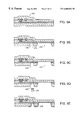
- FIGS. 6A-6D Another preferred embodiment is shown in the process sequence of FIGS. 6A-6D.
- the circuit 80 is prepared through data line metalization as shown in FIG. 6A.
- a via 82 is opened through the oxide layer 81 to the single crystal silicon material (FIG. 6 B).
- the via openings for each transistor circuit in the matrix are then prepared for pixel electrode material deposition by either a sputter etch, a surface treatment 84 of the silicon using a palladium or platinum chloride, or alternatively, by deposition of a thin nickel layer.
- the pixel electrode material 86 which in the example is ITO, is formed on or over the prepared surface of the silicon exposed by the via (FIG. 6 C), followed by the deposition of the passivation layer 88 (FIG. 6 D).
- FIG. 7 illustrates an embodiment similar to that formed in FIGS. 6A-6D except that the via is filled with deposited metal plug or contact filler 90 .
- the filler can be an electroless plated nickel or be formed by chemical vapor deposition of a metal such as tungsten in a step separate from the formation of the other transistor contact. This is followed by deposition and patterning of an ITO electrode 92 on or over the filler 90 , the transistor sidewall and the pixel electrode area. This process provides for use of a different material for the pixel electrode contact than that used for data line metalization. This provides improved conduction to the ITO electrode material.
- FIGS. 8A-8D A process sequence illustrating this embodiment is shown in FIGS. 8A-8D. Note that the transfer substrate is used but not shown in the figures for clarity.
- a transferred active matrix circuit is prepared as shown in FIG. 8A.
- a via 102 is formed through the insulator 12 to expose a contact area 104 of the silicon in the transistor circuit as shown in FIG. 8 B.
- Surface treatment 106 of the exposed silicon as described previously can be applied if needed, also as shown in FIG. 8B.
- a conductive transparent electrode material 108 is then deposited and patterned to make electrical contact to the transistor circuit through the via 102 and simultaneously form the pixel electrodes (FIG. 8 C).
- an additional metal layer 110 or other conductive material can be formed between the electrode material 108 and the contact area 104 to improve conductivity.
- Layer 110 can also act as an opaque light shield on one side of the transistor circuit.
- a separate light shield region 120 can also be formed on the second side of the circuit in a manner similar to that described in greater detail in U.S. Pat. No. 5,256,562, the contents of which were previously incorporated by reference.
- FIGS. 9A-9E A transferred circuit 200 is shown in FIG. 9 A.
- the pixel electrode area is defined by the removal of the insulator region 210 to form apertures in the insulating layer.
- the contact area 215 is defined by via 230 shown in FIG. 9 B.
- the single crystal silicon is removed from the exposed pixel electrode area 220 in FIG. 9C, and the via 230 to the transistor circuit is optionally treated 240 as shown in FIG. 9 D.
- the transparent pixel electrode material 250 is then formed in the via 230 and the pixel electrode area 220 as shown in FIG. 9 E.
- the device is now ready for final display fabrication as described previously.
- FIGS. 10A-10B involves exposing a portion 300 of the single crystal silicon layer in which the transistor circuit is formed in the step shown in FIG. 9B, and masking the portion of the circuit during removal of the silicon to form the structure shown in FIG. 10 A.
- the conductive transparent electrode 310 is formed as shown in FIG. 10B that can directly contact the transistor circuit at contact area 300 , or the exposed silicon can be treated prior to contact formation as described previously.
- a further passivation layer (not shown) can also be added to cover the pixel electrode 310 to provide electrical isolation, and planarization of the pixel area.
- FIGS. 11A-11B The fabrication of a titanium dioxide pixel electrode is shown in FIGS. 11A-11B. This process or other metal oxides or metal nitrides can be used in any of the processes described elsewhere herein for forming pixel electrodes after or during transistor fabrication. In this process two electrode layers 330 , 340 are formed which are separated by an insulator 345 .
- First layer 330 acts as a ground plane and is electrically connected to the electrode 350 on the opposite side of the liquid crystal material 360 .
- This structure provides improved electrical isolation for the pixel electrode 340 that actuates the pixel element.
- An interconnect 348 is used to connect electrode 340 to the transistor in an area outside of the region occupied by electrode 330 .
- Color filters can be used in this embodiment as well.
- FIGS. 12A-12E illustrate another preferred process flow sequence for fabrication of a color filter system that can be used without limitation, for example with transmissive displays, emissive displays, head mounted displays or projection displays.
- the color filters are polyimide color filters. More specifically, the color filter illustrated is a PiC Green 02 polyimide filter material available from Brewer Science, Inc. of Rolla, Miss. Blue and red filter materials are also available from the same source and use substantially the same processing sequence as described hereinafter. As described elsewhere herein, other color separation and selection techniques can also be employed that are compatible with conventional semiconductor photolithography and processing methods.
- a pixel element 410 having an electrode 412 and a transistor 414 is formed on an insulating layer 415 .
- An optional nitride layer 420 can be formed over the pixel element 410 , as shown in FIG. 12 B.
- An optional adhesion promoter (not shown) can next be coated and baked onto the nitride layer 420 .
- the adhesion promotor can be APX K-1, also provided by Brewer Science, Inc., which can be spun onto the wafer at 5000 RPM, and then baked in an oven. In a preferred embodiment, however, an adhesion promoter is not used.
- a layer of polyimide, such as PiC Green 02 is spun on over the circuit at a speed of 1000-4000 rpm for 90 seconds.
- the resulting structure is shown in FIG. 12 C.
- the polyimide layer 430 is about 0.5 to 5 microns thick. In a preferred embodiment, the polyimide layer 430 is about 1 to 2 microns thick.
- the structure is then subjected to a solvent removal bake at 120° C. for 60 seconds on a hotplate for example. It should be noted that a the particular conditions of the solvent bake is not critical.
- the structure is then subjected to a second or “beta” bake at 175° C. on a hotplate for 90 seconds in vacuum contact. It is critical that the temperature be uniform in the beta bake step because the beta bake defines the develop processing characteristics.
- a photoresist pattern 440 is applied to the structure.
- the positive photoresist is coated, baked and exposed to ultraviolet light 450 using a mask (not shown) at 1.5 to 2 times the normal dosage.
- the pattern is then developed with a standard fluid developer for 40 seconds.
- the developer is preferably a metal ion free developer such as Shipely MF-312.
- the polyimide 430 will develop with the photoresist.
- the structure is then rinsed in water and dried with nitrogen or clean compressed air.
- the photoresist 440 is then removed with a commercially available carbon based solvent, such as Safestrip from Brewer Science, Inc., which is spun onto the structure.
- a commercially available carbon based solvent such as Safestrip from Brewer Science, Inc.
- the resulting color filter structure 435 shown in FIG. 12E is then hard baked between 200° and 280° C. for one hour in an oven. In a preferred embodiment, the baked temperature is 230° C.
- the above process is repeated for the red and the blue color filters to provide a full color liquid crystal display or EL display.
- the spin speed and bake temperature are varied as needed depending upon the size of the color filter element.
- the resulting structure is encapsulated using a layer of silicon nitride, oxynitride or silicon oxide.
- An optically clear polyimide layer can also be used for encapsulation and planarization.
- the circuit can then be transferred onto a second substrate in accordance with previously described procedures depending upon the type of display being fabricated.
- Another preferred embodiment uses red, blue, and green polyimides which incorporate photosensitive material.
- the polyimides are put on, exposed and developed. No photoresist is needed using this process.
- a filter fabrication process using negative photoresist materials is employed to form an array of color filter elements.
- a pigment is dispersed in a negative resist material and applied as a film.
- a negative resist material are commercially available.
- a portion of the film is exposed to light.
- the remainder of the film is masked (not shown) such that it is not exposed to the light.
- the exposed portion of the film is developed in the presence of the light to form a first color filter element.
- the undeveloped portion of the film is removed, leaving a pattern of first color filter elements adjacent to each pixel electrode.
- Second and third color filter elements are formed in a similar manner as the first color filter elements.
- a matrix array of opaque (or black) elements can be formed over or adjacent the transistor region of each pixel electrode as well as over the interprise spaces.
- Each opaque element serves to absorb light and provide a uniform background.
- a color filter array is formed adjacent to the active matrix circuitry by applying a color photographic development process for each color which uses color-coupler containing developers.
- a black and white silver halide emulsion layer is formed adjacent to each pixel electrode of the active matrix.
- the formation of color filter elements utilizing a silver halide emulsion can be reviewed in greater detail in U.S. Pat. No. 4,400,454.
- An isolation layer such as SiO 2 , is formed over the active matrix and patterned to expose the portion of the emulsion layer adjacent each pixel electrode. This portion of the emulsion layer is exposed to light to provide silver particles.
- a first developer containing a color coupler is added to each exposed region of the emulsion layer. As such, a dye of a first color is then formed in each region. Next, the silver is removed by bleaching or rehalogenating for each region.
- Portions of the unexposed silver halide emulsion layer electrode adjacent to each pixel are then exposed to light through a patterned isolation layer formed over the active matrix.
- a second developer containing a color coupler is added to each exposed region of the emulsion layer to form a dye of a second color in each region.
- the silver is removed by bleaching or rehalogenating for each region.
- the remaining portions of the unexposed silver halide emulsion layer adjacent to the pixel electrodes are then exposed to light through a patterned isolation layer.
- a third developer containing a color coupler is added to each exposed region of the emulsion layer to form a dye of a third color in each region.
- the silver is removed by bleaching or rehalogenating for each region.
- the isolation layer is removed and any silver halide remaining in the emulsion layer is removed by fixing. An array of color filter elements are thus formed adjacent to each pixel electrode.
- a color filter array can be formed by applying a color photographic development process which uses developers containing dye developers. To accomplish this, the above-described process is performed using developers containing dye developers instead of developers containing color couplers. After processing such as that described in the Figures the thin film with the formed color filter elements can than be transferred, if necessary, for further processing prior to final display fabrication.
- An alternative embodiment is to put the color filter system on one side of the transfer substrate such as the glass substrate 500 in a transmissive liquid crystal display as illustrated in the process sequence of FIGS. 13A-13C. Processing is the same to form the colored pixels.
- a formed green color filter element 510 is shown in FIG. 13 A.
- the blue and red filter elements are then formed as shown in FIG. 13 B and the circuit is then aligned with and transferred onto the color filter substrate 500 with the pixel electrodes and color filter elements bonded by an adhesive 540 .
- a liquid crystal display is fabricated in accordance with this method is shown in the cross sectional view of FIG. 13C where pixel electrodes 550 , 560 are separated from correlated aligned color filter elements 510 , 520 by a thin adhesive layer 540 that is about 1-5 microns thick.
- Transistors 580 actuate the electrodes to control the transmission of light at each pixel through the liquid crystal material 590 .
- FIGS. 14A-14C illustratas a process similar to that shown in FIGS. 8A-8D, except that color filter elements 600 are fabricated after transistor 100 formation and prior to transfer and fabrication of the pixel electrodes on the opposite side of the insulator 12 (FIG. 14 A).
- FIG. 14B shows the structure after transfer onto substrate 620 with adhesive 610 and exposure of transistor contact 104 .
- FIG. 14C shows the device after electrode 108 formation on the opposite side of insulator 12 .
- the electrode 108 can be formed on the opposite side of insulator 12 using the various methods previously described herein.
- a transistor circuit 714 is formed on a insulating layer 715 .
- An insulator 720 is deposited over the transistor.
- An electrode 712 is formed over the insulator 720 or adhesive.
- the electrode 712 is interconnected to the transistor circuit 714 by an interconnect 713 through the insulator layer 720 .
- An EL stack 730 employing a white phosphor layer and color filter elements as described elsewhere herein, and in U.S. Ser. No. 07/943,896 filed on Sep. 11, 1992 which is incorporated herein by reference, are then fabricated over electrode 712 , either by monolithic fabrication or transfer and alignment on a prefabricated EL stack 730 or incorporation into a liquid crystal display.
- FIGS. 16-18 are top views of patterned pixel electrodes for three preferred embodiments of an active matrix of a flat panel display.
- regions of the silicon material in an SOI structure are removed to form a pattern in each electrode.
- the electrode pattern can be in the form of a checkerboard pattern as shown in FIG. 16 in which an aray of separated squares have been removed, a linear grid as shown in FIGS. 17 and 18, a serpentine shape, or other suitable aperture geometry to reduce transmission loss through each pixel electrode.
- the individual pixel electrode 810 as shown in FIG. 16 initially comprises a solid layer of single crystal silicon. However, the element is processed such that areas 820 of silicon are removed and regions 815 of silicon remain. As shown in FIG.
- the resulting pixel electrode 830 resembles a grid.
- the open areas 835 have a width (W 1 ) in a range of 1-6 microns and the strips 840 of electrode material have a width (W 2 ) of in a range of about 1-6 microns.
- W 1 width
- W 2 width
- Areas 835 and stips 840 in FIG. 17 both have widths of about 2.5 microns.
- the pixel electrode 850 has removed areas or apertures 860 and strips 870 of electrode material that are both about 3 microns in width.
- the grid provides an aperture through each pixel electrode that improves transmission of light by reducing interference effects and also reducing reflection, absorption, and scattering caused by the pixel material.
- One advantage of the grid-shaped pixels is the increased light transmission through the active matrix, which results in brighter displayed images.
- Another advantage is that grid-shaped pixels minimize thickness variations in the single crystal silicon layer. These thickness variations cause light absorption or interference, which reduces the light transmission through the active matrix. By minimizing thickness variations, brighter displayed images can be provided.
Abstract
Description
Claims (10)
Priority Applications (1)
| Application Number | Priority Date | Filing Date | Title |
|---|---|---|---|
| US08/716,409 US6608654B2 (en) | 1992-09-11 | 1995-03-17 | Methods of fabricating active matrix pixel electrodes |
Applications Claiming Priority (3)
| Application Number | Priority Date | Filing Date | Title |
|---|---|---|---|
| US07/944,207 US5444557A (en) | 1990-12-31 | 1992-09-11 | Single crystal silicon arrayed devices for projection displays |
| PCT/US1995/003365 WO1995025983A1 (en) | 1992-09-11 | 1995-03-17 | Methods of fabricating active matrix pixel electrodes |
| US08/716,409 US6608654B2 (en) | 1992-09-11 | 1995-03-17 | Methods of fabricating active matrix pixel electrodes |
Related Parent Applications (1)
| Application Number | Title | Priority Date | Filing Date |
|---|---|---|---|
| US07/944,207 Continuation-In-Part US5444557A (en) | 1990-12-31 | 1992-09-11 | Single crystal silicon arrayed devices for projection displays |
Publications (2)
| Publication Number | Publication Date |
|---|---|
| US20020030767A1 US20020030767A1 (en) | 2002-03-14 |
| US6608654B2 true US6608654B2 (en) | 2003-08-19 |
Family
ID=25480998
Family Applications (1)
| Application Number | Title | Priority Date | Filing Date |
|---|---|---|---|
| US08/716,409 Expired - Fee Related US6608654B2 (en) | 1992-09-11 | 1995-03-17 | Methods of fabricating active matrix pixel electrodes |
Country Status (1)
| Country | Link |
|---|---|
| US (1) | US6608654B2 (en) |
Cited By (15)
| Publication number | Priority date | Publication date | Assignee | Title |
|---|---|---|---|---|
| US20030095116A1 (en) * | 1998-06-17 | 2003-05-22 | Semiconductor Energy Laboratory Co. Ltd., A Japanese Corporation | Reflective type semiconductor display device |
| US20040257357A1 (en) * | 1996-09-27 | 2004-12-23 | Semiconductor Energy Laboratory Co., Ltd., A Japan Corporation | Electrooptical device and method of fabricating the same |
| US20050023525A1 (en) * | 2000-09-14 | 2005-02-03 | Semiconductor Energy Laboratory Co. Ltd., A Japan Corporation | Semiconductor device and manufacturing method thereof |
| US7274413B1 (en) * | 2002-12-06 | 2007-09-25 | United States Of America As Represented By The Secretary Of The Navy | Flexible video display apparatus and method |
| US20080049159A1 (en) * | 2006-08-16 | 2008-02-28 | Bor-Yeu Tsaur | Display system with single crystal Si thin film transistors |
| US20080225212A1 (en) * | 2007-03-13 | 2008-09-18 | Ong Hiap L | Pixel designs for multi-domain vertical alignment liquid crystal display |
| US20090152539A1 (en) * | 2002-10-18 | 2009-06-18 | Semiconductor Energy Laboratory Co., Ltd. | Semiconductor Apparatus and Fabrication Method of the Same |
| US20110012818A1 (en) * | 1999-06-21 | 2011-01-20 | Semiconductor Energy Laboratory Co., Ltd. | El display device, driving method thereof, and electronic equipment provided with the el display device |
| US8344992B2 (en) | 2000-02-29 | 2013-01-01 | Semiconductor Energy Laboratory Co., Ltd. | Display device and method for fabricating the same |
| US8344369B2 (en) | 2001-12-28 | 2013-01-01 | Semiconductor Energy Laboratory Co., Ltd. | Vehicle that includes a display panel having a curved surface |
| US8669925B2 (en) | 2000-05-12 | 2014-03-11 | Semiconductor Energy Laboratory Co., Ltd. | Light-emitting device and electric appliance |
| US9493119B2 (en) | 2001-11-30 | 2016-11-15 | Semiconductor Energy Laboratory Co., Ltd. | Vehicle, display device and manufacturing method for a semiconductor device |
| US9837451B2 (en) | 1999-04-27 | 2017-12-05 | Semiconductor Energy Laboratory Co., Ltd. | Electronic device and electronic apparatus |
| US9947568B2 (en) | 2013-02-20 | 2018-04-17 | Semiconductor Energy Laboratory Co., Ltd. | Peeling method, semiconductor device, and peeling apparatus |
| US10189048B2 (en) | 2013-12-12 | 2019-01-29 | Semiconductor Energy Laboratory Co., Ltd. | Peeling method and peeling apparatus |
Families Citing this family (6)
| Publication number | Priority date | Publication date | Assignee | Title |
|---|---|---|---|---|
| US8334451B2 (en) * | 2003-10-03 | 2012-12-18 | Ixys Corporation | Discrete and integrated photo voltaic solar cells |
| JP4970242B2 (en) * | 2004-03-20 | 2012-07-04 | ヒューレット−パッカード デベロップメント カンパニー エル.ピー. | Application of color elements and bus bars to display substrates |
| JP4213616B2 (en) * | 2004-03-31 | 2009-01-21 | 大日本印刷株式会社 | Base film for liquid crystal panel, functional film for liquid crystal panel, method for producing functional film, and apparatus for producing functional film |
| JP2007286150A (en) * | 2006-04-13 | 2007-11-01 | Idemitsu Kosan Co Ltd | Electrooptical device, and tft substrate for controlling electric current and method of manufacturing the same |
| CN101878534B (en) * | 2008-01-21 | 2012-07-04 | 夏普株式会社 | Semiconductor device and display device |
| US10114263B2 (en) * | 2015-12-18 | 2018-10-30 | Semiconductor Energy Laboratory Co., Ltd. | Display device |
Citations (30)
| Publication number | Priority date | Publication date | Assignee | Title |
|---|---|---|---|---|
| US4024626A (en) | 1974-12-09 | 1977-05-24 | Hughes Aircraft Company | Method of making integrated transistor matrix for flat panel liquid crystal display |
| US4429305A (en) | 1979-05-30 | 1984-01-31 | Kabushiki, Kaisha Suwa Seikosha | Liquid crystal display system |
| EP0248905A1 (en) | 1985-02-05 | 1987-12-16 | Kyodo Printing Co., Ltd. | Method of producing a color filter |
| US4727047A (en) | 1980-04-10 | 1988-02-23 | Massachusetts Institute Of Technology | Method of producing sheets of crystalline material |
| JPS6355529A (en) | 1986-08-25 | 1988-03-10 | Nec Corp | Active matrix liquid crystal display device and its production |
| US4733948A (en) * | 1984-12-20 | 1988-03-29 | Canon Kabushiki Kaisha | Color liquid crystal display with light intercepting member |
| US4740782A (en) | 1982-07-12 | 1988-04-26 | Hosiden Electronics Co., Ltd. | Dot-matrix liquid crystal display |
| JPS63101830A (en) | 1986-10-17 | 1988-05-06 | Nec Corp | Active matrix liquid crystal display device and its manufacture |
| US4770498A (en) | 1982-07-12 | 1988-09-13 | Hosiden Electronics Co., Ltd. | Dot-matrix liquid crystal display |
| JPS6438727A (en) | 1987-08-04 | 1989-02-09 | Nec Corp | Transistor array substrate for display |
| US4808983A (en) | 1984-02-01 | 1989-02-28 | The Secretary Of State For Defence In Her Majesty's Government Of The United Kingdom Of Great Britain And Northern Ireland | Flat-panel display and a process for its manufacture |
| US4838654A (en) | 1986-10-17 | 1989-06-13 | Nec Corporation | Liquid crystal display device having display and driver sections on a single board |
| JPH01195421A (en) | 1988-01-30 | 1989-08-07 | Nec Home Electron Ltd | Manufacture of liquid crystal display device |
| US4935792A (en) | 1985-11-27 | 1990-06-19 | Sharp Kabushiki Kaisha | Thin film transistor array |
| US4952031A (en) | 1987-06-19 | 1990-08-28 | Victor Company Of Japan, Ltd. | Liquid crystal display device |
| US4965565A (en) | 1987-05-06 | 1990-10-23 | Nec Corporation | Liquid crystal display panel having a thin-film transistor array for displaying a high quality picture |
| US5020881A (en) | 1988-01-26 | 1991-06-04 | Canon Kabushiki Kaisha | Light modulating device with optical switching unit of laminated insulating and conductive layers |
| US5056895A (en) | 1990-05-21 | 1991-10-15 | Greyhawk Systems, Inc. | Active matrix liquid crystal liquid crystal light valve including a dielectric mirror upon a leveling layer and having fringing fields |
| US5073772A (en) | 1988-02-06 | 1991-12-17 | Sharp Kabushiki Kaisha | Liquid crystal display device |
| US5095304A (en) | 1988-10-07 | 1992-03-10 | U.S. Philips Corporation | Matrix display device |
| EP0474474A2 (en) | 1990-09-05 | 1992-03-11 | Seiko Instruments Inc. | Semiconductor light valve device and process for fabricating the same |
| EP0486318A1 (en) | 1990-11-15 | 1992-05-20 | Seiko Instruments Inc. | Semiconductor device for use in a light valve device, and process for manufacturing the same |
| US5117298A (en) | 1988-09-20 | 1992-05-26 | Nec Corporation | Active matrix liquid crystal display with reduced flickers |
| WO1992012453A1 (en) | 1990-12-31 | 1992-07-23 | Kopin Corporation | Single crystal silicon arrayed devices for display panels |
| US5166816A (en) | 1988-11-30 | 1992-11-24 | Nec Corporation | Liquid crystal display panel with reduced pixel defects |
| US5184235A (en) | 1988-11-18 | 1993-02-02 | Nec Corporation | Active matrix liquid crystal display panel with an electrostatic protection circuit |
| US5191453A (en) | 1989-08-23 | 1993-03-02 | Nec Corporation | Active matrix substrate for liquid-crystal display and method of fabricating the active matrix substrate |
| US5256562A (en) | 1990-12-31 | 1993-10-26 | Kopin Corporation | Method for manufacturing a semiconductor device using a circuit transfer film |
| US5258320A (en) | 1990-12-31 | 1993-11-02 | Kopin Corporation | Single crystal silicon arrayed devices for display panels |
| US5376561A (en) | 1990-12-31 | 1994-12-27 | Kopin Corporation | High density electronic circuit modules |
-
1995
- 1995-03-17 US US08/716,409 patent/US6608654B2/en not_active Expired - Fee Related
Patent Citations (33)
| Publication number | Priority date | Publication date | Assignee | Title |
|---|---|---|---|---|
| US4024626A (en) | 1974-12-09 | 1977-05-24 | Hughes Aircraft Company | Method of making integrated transistor matrix for flat panel liquid crystal display |
| US4429305A (en) | 1979-05-30 | 1984-01-31 | Kabushiki, Kaisha Suwa Seikosha | Liquid crystal display system |
| US4727047A (en) | 1980-04-10 | 1988-02-23 | Massachusetts Institute Of Technology | Method of producing sheets of crystalline material |
| US4740782A (en) | 1982-07-12 | 1988-04-26 | Hosiden Electronics Co., Ltd. | Dot-matrix liquid crystal display |
| US4770498A (en) | 1982-07-12 | 1988-09-13 | Hosiden Electronics Co., Ltd. | Dot-matrix liquid crystal display |
| US4808983A (en) | 1984-02-01 | 1989-02-28 | The Secretary Of State For Defence In Her Majesty's Government Of The United Kingdom Of Great Britain And Northern Ireland | Flat-panel display and a process for its manufacture |
| US4733948A (en) * | 1984-12-20 | 1988-03-29 | Canon Kabushiki Kaisha | Color liquid crystal display with light intercepting member |
| EP0248905A1 (en) | 1985-02-05 | 1987-12-16 | Kyodo Printing Co., Ltd. | Method of producing a color filter |
| US4935792A (en) | 1985-11-27 | 1990-06-19 | Sharp Kabushiki Kaisha | Thin film transistor array |
| JPS6355529A (en) | 1986-08-25 | 1988-03-10 | Nec Corp | Active matrix liquid crystal display device and its production |
| JPS63101830A (en) | 1986-10-17 | 1988-05-06 | Nec Corp | Active matrix liquid crystal display device and its manufacture |
| US4838654A (en) | 1986-10-17 | 1989-06-13 | Nec Corporation | Liquid crystal display device having display and driver sections on a single board |
| US4965565A (en) | 1987-05-06 | 1990-10-23 | Nec Corporation | Liquid crystal display panel having a thin-film transistor array for displaying a high quality picture |
| US4952031A (en) | 1987-06-19 | 1990-08-28 | Victor Company Of Japan, Ltd. | Liquid crystal display device |
| JPS6438727A (en) | 1987-08-04 | 1989-02-09 | Nec Corp | Transistor array substrate for display |
| US5020881A (en) | 1988-01-26 | 1991-06-04 | Canon Kabushiki Kaisha | Light modulating device with optical switching unit of laminated insulating and conductive layers |
| JPH01195421A (en) | 1988-01-30 | 1989-08-07 | Nec Home Electron Ltd | Manufacture of liquid crystal display device |
| US5073772A (en) | 1988-02-06 | 1991-12-17 | Sharp Kabushiki Kaisha | Liquid crystal display device |
| US5117298A (en) | 1988-09-20 | 1992-05-26 | Nec Corporation | Active matrix liquid crystal display with reduced flickers |
| US5095304A (en) | 1988-10-07 | 1992-03-10 | U.S. Philips Corporation | Matrix display device |
| US5184235A (en) | 1988-11-18 | 1993-02-02 | Nec Corporation | Active matrix liquid crystal display panel with an electrostatic protection circuit |
| US5166816A (en) | 1988-11-30 | 1992-11-24 | Nec Corporation | Liquid crystal display panel with reduced pixel defects |
| US5191453A (en) | 1989-08-23 | 1993-03-02 | Nec Corporation | Active matrix substrate for liquid-crystal display and method of fabricating the active matrix substrate |
| US5056895A (en) | 1990-05-21 | 1991-10-15 | Greyhawk Systems, Inc. | Active matrix liquid crystal liquid crystal light valve including a dielectric mirror upon a leveling layer and having fringing fields |
| EP0474474A2 (en) | 1990-09-05 | 1992-03-11 | Seiko Instruments Inc. | Semiconductor light valve device and process for fabricating the same |
| EP0486318A1 (en) | 1990-11-15 | 1992-05-20 | Seiko Instruments Inc. | Semiconductor device for use in a light valve device, and process for manufacturing the same |
| WO1992012453A1 (en) | 1990-12-31 | 1992-07-23 | Kopin Corporation | Single crystal silicon arrayed devices for display panels |
| US5206749A (en) | 1990-12-31 | 1993-04-27 | Kopin Corporation | Liquid crystal display having essentially single crystal transistors pixels and driving circuits |
| US5256562A (en) | 1990-12-31 | 1993-10-26 | Kopin Corporation | Method for manufacturing a semiconductor device using a circuit transfer film |
| US5258320A (en) | 1990-12-31 | 1993-11-02 | Kopin Corporation | Single crystal silicon arrayed devices for display panels |
| US5317236A (en) | 1990-12-31 | 1994-05-31 | Kopin Corporation | Single crystal silicon arrayed devices for display panels |
| US5376561A (en) | 1990-12-31 | 1994-12-27 | Kopin Corporation | High density electronic circuit modules |
| US5377031A (en) | 1990-12-31 | 1994-12-27 | Kopin Corporation | Single crystal silicon tiles for liquid crystal display panels including light shielding layers |
Non-Patent Citations (3)
| Title |
|---|
| Laakso et al., "A 9 Inch Diagonal, Compact, Multicolor TFEL Display", 1991 International Display Research Conference, pp. 43-44. |
| Matsumoto et al. "Liquid Ctystal Displays (LCD)" In Electronic Display Devices (John Wiley & Sons) (1984) pp. 29-84. |
| Sumiyoshi et al. "Device layer Transferred Poly Si TFT Array For High Resolution Liquid Crystal Projector" IEDM, (1989) pp. 165-168. |
Cited By (52)
| Publication number | Priority date | Publication date | Assignee | Title |
|---|---|---|---|---|
| US7489291B2 (en) | 1996-09-27 | 2009-02-10 | Semiconductor Energy Laboratory Co., Ltd. | Electrooptical device and method of fabricating the same |
| US8564575B2 (en) | 1996-09-27 | 2013-10-22 | Semiconductor Energy Laboratory Co., Ltd. | Electrooptical device and method of fabricating the same |
| US20050088433A1 (en) * | 1996-09-27 | 2005-04-28 | Semiconductor Energy Laboratory Co., Ltd., A Japanese Corporation | Electrooptical device and method of fabricating the same |
| US20050093852A1 (en) * | 1996-09-27 | 2005-05-05 | Semiconductor Energy Laboratory Co., Ltd. A Japan Corporation | Electrooptical device and method of fabricating the same |
| US7532208B2 (en) | 1996-09-27 | 2009-05-12 | Semiconductor Energy Laboratory Co., Ltd. | Electrooptical device and method of fabricating the same |
| US20040257357A1 (en) * | 1996-09-27 | 2004-12-23 | Semiconductor Energy Laboratory Co., Ltd., A Japan Corporation | Electrooptical device and method of fabricating the same |
| US7268777B2 (en) | 1996-09-27 | 2007-09-11 | Semiconductor Energy Laboratory Co., Ltd. | Electrooptical device and method of fabricating the same |
| US20090195523A1 (en) * | 1996-09-27 | 2009-08-06 | Semiconductor Energy Laboratory Co., Ltd. | Electrooptical Device and Method of Fabricating the Same |
| US7408534B2 (en) | 1998-06-17 | 2008-08-05 | Semiconductor Energy Laboratory Co., Ltd. | Reflective type semiconductor display device |
| US20030095116A1 (en) * | 1998-06-17 | 2003-05-22 | Semiconductor Energy Laboratory Co. Ltd., A Japanese Corporation | Reflective type semiconductor display device |
| US9837451B2 (en) | 1999-04-27 | 2017-12-05 | Semiconductor Energy Laboratory Co., Ltd. | Electronic device and electronic apparatus |
| US8830146B2 (en) | 1999-06-21 | 2014-09-09 | Semiconductor Energy Laboratory Co., Ltd. | EL display device, driving method thereof, and electronic equipment provided with the EL display device |
| US8941565B2 (en) | 1999-06-21 | 2015-01-27 | Semiconductor Energy Laboratory Co., Ltd. | EL display device, driving method thereof, and electronic equipment provided with the EL display device |
| US20110012818A1 (en) * | 1999-06-21 | 2011-01-20 | Semiconductor Energy Laboratory Co., Ltd. | El display device, driving method thereof, and electronic equipment provided with the el display device |
| US9659524B2 (en) | 1999-06-21 | 2017-05-23 | Semiconductor Energy Laboratory Co., Ltd. | Light-emitting device including substrate having cavity, and method for fabricating the light-emitting device |
| US8558773B2 (en) | 1999-06-21 | 2013-10-15 | Semiconductor Energy Laboratory Co., Ltd. | EL display device, driving method thereof, and electronic equipment provided with the EL display device |
| US8405594B2 (en) | 1999-06-21 | 2013-03-26 | Semiconductor Energy Laboratory Co., Ltd. | EL display device, driving method thereof, and electronic equipment provided with the EL display device |
| US9263476B2 (en) | 2000-02-29 | 2016-02-16 | Semiconductor Energy Laboratory Co., Ltd. | Display device and method for fabricating the same |
| US8717262B2 (en) | 2000-02-29 | 2014-05-06 | Semiconductor Energy Laboratory Co., Ltd. | Display device and method for fabricating the same |
| US8344992B2 (en) | 2000-02-29 | 2013-01-01 | Semiconductor Energy Laboratory Co., Ltd. | Display device and method for fabricating the same |
| US8669925B2 (en) | 2000-05-12 | 2014-03-11 | Semiconductor Energy Laboratory Co., Ltd. | Light-emitting device and electric appliance |
| US20070018164A1 (en) * | 2000-09-14 | 2007-01-25 | Semiconductor Energy Laboratory Co., Ltd. | Semiconductor Device and Manufacturing Method Thereof |
| US20050023525A1 (en) * | 2000-09-14 | 2005-02-03 | Semiconductor Energy Laboratory Co. Ltd., A Japan Corporation | Semiconductor device and manufacturing method thereof |
| US7109071B2 (en) * | 2000-09-14 | 2006-09-19 | Semiconductor Energy Laboratory Co., Ltd. | Semiconductor device and manufacturing method thereof |
| US20080283838A1 (en) * | 2000-09-14 | 2008-11-20 | Semiconductor Energy Laboratory Co., Ltd. | Semiconductor device and manufacturing method thereof |
| US7408193B2 (en) | 2000-09-14 | 2008-08-05 | Semiconductor Energy Laboratory Co., Ltd. | Semiconductor device and manufacturing method thereof |
| US7642555B2 (en) | 2000-09-14 | 2010-01-05 | Semiconductor Energy Laboratory Co., Ltd. | Semiconductor device |
| US10629637B2 (en) | 2001-11-30 | 2020-04-21 | Semiconductor Energy Laboratory Co., Ltd. | Vehicle, display device and manufacturing method for a semiconductor device |
| US10957723B2 (en) | 2001-11-30 | 2021-03-23 | Semiconductor Energy Laboratory Co., Ltd. | Vehicle, display device and manufacturing method for a semiconductor device |
| US10325940B2 (en) | 2001-11-30 | 2019-06-18 | Semiconductor Energy Laboratory Co., Ltd. | Vehicle, display device and manufacturing method for a semiconductor device |
| US9493119B2 (en) | 2001-11-30 | 2016-11-15 | Semiconductor Energy Laboratory Co., Ltd. | Vehicle, display device and manufacturing method for a semiconductor device |
| US8344369B2 (en) | 2001-12-28 | 2013-01-01 | Semiconductor Energy Laboratory Co., Ltd. | Vehicle that includes a display panel having a curved surface |
| US8610118B2 (en) | 2001-12-28 | 2013-12-17 | Semiconductor Energy Laboratory Co., Ltd. | Flexible display panel having curvature that matches curved surface of vehicle part |
| US9536901B2 (en) | 2001-12-28 | 2017-01-03 | Semiconductor Energy Laboratory Co., Ltd. | Method for fabricating a semiconductor device by bonding a layer to a support with curvature |
| US9337341B2 (en) | 2001-12-28 | 2016-05-10 | Semiconductor Energy Laboratory Co., Ltd. | Semiconductor device having aluminum-containing layer between two curved substrates |
| US9123595B2 (en) | 2001-12-28 | 2015-09-01 | Semiconductor Energy Laboratory Co., Ltd. | Method for fabricating a semiconductor device by bonding a layer to a support with curvature |
| US9093324B2 (en) | 2002-10-18 | 2015-07-28 | Semiconductor Energy Laboratory Co., Ltd. | Semiconductor apparatus and fabrication method of the same |
| US8013335B2 (en) | 2002-10-18 | 2011-09-06 | Semiconductor Energy Laboratory Co., Ltd. | Semiconductor apparatus and fabrication method of the same |
| US20110180797A1 (en) * | 2002-10-18 | 2011-07-28 | Semiconductor Energy Laboratory Co., Ltd. | Semiconductor Apparatus and Fabrication Method of the Same |
| US8134153B2 (en) | 2002-10-18 | 2012-03-13 | Semiconductor Energy Laboratory Co., Ltd. | Semiconductor apparatus and fabrication method of the same |
| US20090152539A1 (en) * | 2002-10-18 | 2009-06-18 | Semiconductor Energy Laboratory Co., Ltd. | Semiconductor Apparatus and Fabrication Method of the Same |
| US8525171B2 (en) | 2002-10-18 | 2013-09-03 | Semiconductor Energy Laboratory Co., Ltd. | Semiconductor apparatus and fabrication method of the same |
| US7274413B1 (en) * | 2002-12-06 | 2007-09-25 | United States Of America As Represented By The Secretary Of The Navy | Flexible video display apparatus and method |
| US7768611B2 (en) | 2006-08-16 | 2010-08-03 | Kopin Corporation | Display system with single crystal SI thin film transistors |
| US20100259517A1 (en) * | 2006-08-16 | 2010-10-14 | Kopin Corporation | Display System with Single Crystal Si Thin Film Transistors |
| US20080049159A1 (en) * | 2006-08-16 | 2008-02-28 | Bor-Yeu Tsaur | Display system with single crystal Si thin film transistors |
| US8072406B2 (en) | 2006-08-16 | 2011-12-06 | Kopin Corporation | Display system with single crystal Si thin film transistors |
| US20080225212A1 (en) * | 2007-03-13 | 2008-09-18 | Ong Hiap L | Pixel designs for multi-domain vertical alignment liquid crystal display |
| US9947568B2 (en) | 2013-02-20 | 2018-04-17 | Semiconductor Energy Laboratory Co., Ltd. | Peeling method, semiconductor device, and peeling apparatus |
| US10636692B2 (en) | 2013-02-20 | 2020-04-28 | Semiconductor Energy Laboratory Co., Ltd. | Peeling method, semiconductor device, and peeling apparatus |
| US11355382B2 (en) | 2013-02-20 | 2022-06-07 | Semiconductor Energy Laboratory Co., Ltd. | Peeling method, semiconductor device, and peeling apparatus |
| US10189048B2 (en) | 2013-12-12 | 2019-01-29 | Semiconductor Energy Laboratory Co., Ltd. | Peeling method and peeling apparatus |
Also Published As
| Publication number | Publication date |
|---|---|
| US20020030767A1 (en) | 2002-03-14 |
Similar Documents
| Publication | Publication Date | Title |
|---|---|---|
| US5705424A (en) | Process of fabricating active matrix pixel electrodes | |
| US6608654B2 (en) | Methods of fabricating active matrix pixel electrodes | |
| US6162654A (en) | Display and method of producing the display | |
| JP3240858B2 (en) | Color display | |
| US5721601A (en) | Display units having two insolating films and a planarizing film and process for producing the same | |
| US7019329B2 (en) | Semiconductor device and manufacturing method thereof | |
| EP0725303B1 (en) | Liquid crystal display device | |
| US6734940B2 (en) | Semiconductor device, electro-optical device substrate, liquid crystal device substrate and manufacturing method therefor, liquid crystal device, and projection liquid crystal display device and electronic apparatus using the liquid crystal device | |
| KR100490496B1 (en) | An electrooptic device and method for manufacturing electrooptic device, projection type display device, and electronic apparatus | |
| TW562961B (en) | Liquid crystal display device | |
| US20040241987A1 (en) | Contact portion of semiconductor device, and thin film transistor array panel for display device including the contact portion | |
| US7358104B2 (en) | Contact portion of semiconductor device, and thin film transistor array panel for display device including the contact portion | |
| JPH09311342A (en) | Display device | |
| KR100449772B1 (en) | Electrooptical device, manufacturing method for manufacturing electrooptical device, and electronic equipment | |
| WO2011080879A1 (en) | Active matrix substrate and method for manufacturing same | |
| JP2000275680A (en) | Reflection type liquid crystal display device and display panel using the same | |
| JP3374717B2 (en) | Liquid crystal display panel manufacturing method | |
| US8435722B2 (en) | Method for fabricating liquid crystal display device | |
| JPH0980412A (en) | Manufacture of liquid crystal display device | |
| KR100309213B1 (en) | A method for manufacturing an lcd using a diffarctive expos ure | |
| JPH10170950A (en) | Active matrix type liquid crystal display device and its production | |
| JPH1184363A (en) | Liquid crystal display panel and its production | |
| KR100219477B1 (en) | Reflective thin-film transistor liquid crystal display elements and its manufacturing method | |
| JPH10221716A (en) | Electrode substrate for liquid crystal display element, and liquid crystal display element | |
| KR20080100641A (en) | Liquid crystal display and manufacturing method thereof |
Legal Events
| Date | Code | Title | Description |
|---|---|---|---|
| AS | Assignment |
Owner name: KOPIN CORPORATION, MASSACHUSETTS Free format text: ASSIGNMENT OF ASSIGNORS INTEREST;ASSIGNORS:ZAVRACKY, PAUL M.;VU, DUY-PHACH;DINGLE, BRENDA;AND OTHERS;REEL/FRAME:008409/0420;SIGNING DATES FROM 19961202 TO 19970313 |
|
| FEPP | Fee payment procedure |
Free format text: PAYOR NUMBER ASSIGNED (ORIGINAL EVENT CODE: ASPN); ENTITY STATUS OF PATENT OWNER: SMALL ENTITY |
|
| FPAY | Fee payment |
Year of fee payment: 4 |
|
| FPAY | Fee payment |
Year of fee payment: 8 |
|
| REMI | Maintenance fee reminder mailed | ||
| LAPS | Lapse for failure to pay maintenance fees | ||
| STCH | Information on status: patent discontinuation |
Free format text: PATENT EXPIRED DUE TO NONPAYMENT OF MAINTENANCE FEES UNDER 37 CFR 1.362 |
|
| FP | Lapsed due to failure to pay maintenance fee |
Effective date: 20150819 |