US6604121B1 - Digital division device and method using a reduced-sized lookup table - Google Patents
Digital division device and method using a reduced-sized lookup table Download PDFInfo
- Publication number
- US6604121B1 US6604121B1 US09/451,695 US45169599A US6604121B1 US 6604121 B1 US6604121 B1 US 6604121B1 US 45169599 A US45169599 A US 45169599A US 6604121 B1 US6604121 B1 US 6604121B1
- Authority
- US
- United States
- Prior art keywords
- value
- numerator
- quotient
- denominator
- pqg
- Prior art date
- Legal status (The legal status is an assumption and is not a legal conclusion. Google has not performed a legal analysis and makes no representation as to the accuracy of the status listed.)
- Expired - Fee Related
Links
Images


Classifications
-
- G—PHYSICS
- G06—COMPUTING; CALCULATING OR COUNTING
- G06F—ELECTRIC DIGITAL DATA PROCESSING
- G06F7/00—Methods or arrangements for processing data by operating upon the order or content of the data handled
- G06F7/38—Methods or arrangements for performing computations using exclusively denominational number representation, e.g. using binary, ternary, decimal representation
- G06F7/48—Methods or arrangements for performing computations using exclusively denominational number representation, e.g. using binary, ternary, decimal representation using non-contact-making devices, e.g. tube, solid state device; using unspecified devices
- G06F7/52—Multiplying; Dividing
- G06F7/535—Dividing only
-
- G—PHYSICS
- G11—INFORMATION STORAGE
- G11B—INFORMATION STORAGE BASED ON RELATIVE MOVEMENT BETWEEN RECORD CARRIER AND TRANSDUCER
- G11B5/00—Recording by magnetisation or demagnetisation of a record carrier; Reproducing by magnetic means; Record carriers therefor
- G11B5/48—Disposition or mounting of heads or head supports relative to record carriers ; arrangements of heads, e.g. for scanning the record carrier to increase the relative speed
- G11B5/58—Disposition or mounting of heads or head supports relative to record carriers ; arrangements of heads, e.g. for scanning the record carrier to increase the relative speed with provision for moving the head for the purpose of maintaining alignment of the head relative to the record carrier during transducing operation, e.g. to compensate for surface irregularities of the latter or for track following
- G11B5/596—Disposition or mounting of heads or head supports relative to record carriers ; arrangements of heads, e.g. for scanning the record carrier to increase the relative speed with provision for moving the head for the purpose of maintaining alignment of the head relative to the record carrier during transducing operation, e.g. to compensate for surface irregularities of the latter or for track following for track following on disks
- G11B5/59633—Servo formatting
-
- G—PHYSICS
- G06—COMPUTING; CALCULATING OR COUNTING
- G06F—ELECTRIC DIGITAL DATA PROCESSING
- G06F2207/00—Indexing scheme relating to methods or arrangements for processing data by operating upon the order or content of the data handled
- G06F2207/535—Indexing scheme relating to groups G06F7/535 - G06F7/5375
- G06F2207/5356—Via reciprocal, i.e. calculate reciprocal only, or calculate reciprocal first and then the quotient from the reciprocal and the numerator
Definitions
- X's in the input 226 signify ignored bits, indicating that gates cause the other inputs to be ignored when the left-most bit is zero, saving memory space. Irrespective of the denominator, a numerator bit (left-most) of 0 will produce an output of 0000000.
- Having predetermined limits to the range of allowed denominator values 224 i.e. 32 to 63, in the present example) allows higher accuracy in an implementation of a PQG. Range limits are desirably defined by a priori knowledge of the environment, where possible.
- PQG 540 receives 01-1011 and generates 0010010, which is received and added to 0000010 by accumulator 550 .
- this sum value 565 (equal to 0010100) is latched and control logic 580 ascertains that the division operation is complete, a quotient estimate 595 (indicating a value of 101.00) is generated. Note that this value corresponds well (to 101.001, the expected result), has five bits of precision because this is the limit of a 16-value denominator range. Yet it has been obtained in only 3 iterations (one for each latch/numerator trigger). This speed results from the fact that partial quotients are obtained by a lookup operation (rather than a bona fide calculation) and that each numerator portion comprised more than one bit.
- the servo loop 50 receives the servo information from the head 32 on signal path 52 and this servo information is amplified by a preamp circuit 54 and provided to servo data decode logic circuitry 56 .
- the servo data decode logic circuitry 56 includes an analog to digital converter (ADC) so that selected digital representations of the servo information are provided to a servo microprocessor 58 .
- the servo microprocessor 58 generates the aforementioned SPE signal from the servo information and uses the SPE signal to generate and output a correction signal to VCM control circuitry 60 .
- the amplitude of an A burst signal induced in the head 32 by the A burst pattern 84 will be equal to the amplitude of a B burst signal induced in the head by the B burst pattern 86 .
- the amplitude of a C burst signal induced by the C burst pattern 88 will have a maximum value and the amplitude of a D burst signal from the D burst pattern 90 will be nominally zero.
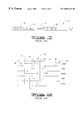
- FIG. 11 shows part of a most-preferred and narrow embodiment of the present invention.
- Latch 301 holds a digitized estimate of PS 1 (labeled 401 ).
- Latch 302 holds a digitized estimate of PS 2 (labeled 402 ).
- Latch 305 holds a digitized estimate of K+1.
- Logic block 361 , comparator 371 , absolute value block 381 , and subtracter 391 generate intermediate calculations 411 , 413 , 461 as shown.
- Logic block 362 , comparator 372 , absolute value block 382 , and subtracter 392 generate intermediate calculations 412 , 414 , 462 as shown.
- Synchronous blocks receive trigger signals from control circuitry 390 , typically on clock cycle boundaries or clock transitions.
- FIG. 12 shows the remainder of the embodiment of FIG. 11, exemplifying exactly how a formula of the form of Eq. 1 can be implemented, and featuring a partial quotient generator that includes static random access memory (SRAM) 325 .
- Intermediate calculations 411 , 412 , 413 , 414 are respectively provided as inputs to 12-bit latches 311 , 312 and shift registers 313 , 314 .
- the shift registers 313 , 314 provide single-bit outputs to two of the three inputs of 3 to 1 multiplexer 321 .
- the latches 311 , 312 provide 12-bit outputs to 2 of the three 12-bit input ports of a 36 to 12 multiplexer 322 .
- the 13 output lines of the multiplexers 321 , 322 are received into the address lines of SRAM 325 , which then provides 12 data lines 431 to a first input of a 12-bit adder 331 .
- the adder output 433 enters a 12-bit latch 333 , which synchronously generates a 12-bit latched divider output value 440 to several places.
- Value 440 becomes an input value 415 to a 12-bit shift register that is coupled to the last input port of multiplexer 321 .
- Value 440 also undergoes bit-shifting, sign-extending, and discarding its least-significant bit, the result becoming an input value 432 to the other port of the adder 331 .
Abstract
Description


Claims (12)
Priority Applications (1)
| Application Number | Priority Date | Filing Date | Title |
|---|---|---|---|
| US09/451,695 US6604121B1 (en) | 1999-05-07 | 1999-11-30 | Digital division device and method using a reduced-sized lookup table |
Applications Claiming Priority (2)
| Application Number | Priority Date | Filing Date | Title |
|---|---|---|---|
| US13299799P | 1999-05-07 | 1999-05-07 | |
| US09/451,695 US6604121B1 (en) | 1999-05-07 | 1999-11-30 | Digital division device and method using a reduced-sized lookup table |
Publications (1)
| Publication Number | Publication Date |
|---|---|
| US6604121B1 true US6604121B1 (en) | 2003-08-05 |
Family
ID=27624841
Family Applications (1)
| Application Number | Title | Priority Date | Filing Date |
|---|---|---|---|
| US09/451,695 Expired - Fee Related US6604121B1 (en) | 1999-05-07 | 1999-11-30 | Digital division device and method using a reduced-sized lookup table |
Country Status (1)
| Country | Link |
|---|---|
| US (1) | US6604121B1 (en) |
Cited By (4)
| Publication number | Priority date | Publication date | Assignee | Title |
|---|---|---|---|---|
| US20020169814A1 (en) * | 2001-05-09 | 2002-11-14 | Fuji Photo Film Co., Ltd. | Calculation method, calculation apparatus and program therefor |
| US7656607B1 (en) | 2008-10-21 | 2010-02-02 | Western Digital Technologies, Inc. | Disk drive comprising a servo accelerator employing a dual state variable memory |
| US7697233B1 (en) | 2008-10-21 | 2010-04-13 | Western Digital Technologies, Inc. | Disk drive comprising a servo accelerator implementing state space equations for a plurality of task objects |
| US8943118B2 (en) | 2012-07-31 | 2015-01-27 | Arm Limited | Data processing apparatus and method for reducing the size of a lookup table |
Citations (9)
| Publication number | Priority date | Publication date | Assignee | Title |
|---|---|---|---|---|
| US4412161A (en) | 1981-04-24 | 1983-10-25 | Iomega Corporation | Digital control of servo circuit |
| US4466077A (en) * | 1981-09-25 | 1984-08-14 | International Business Machines Corporation | Method and apparatus for division employing associative memory |
| US5105378A (en) | 1990-06-25 | 1992-04-14 | Kabushiki Kaisha Toshiba | High-radix divider |
| US5206647A (en) | 1991-06-27 | 1993-04-27 | Hughes Aircraft Company | Low cost AGC function for multiple approximation A/D converters |
| US5576909A (en) | 1995-02-16 | 1996-11-19 | Ministor Peripherals International Limited | Method for positioning a data transducer head in a rotating disk drive data storage device |
| US5602693A (en) | 1994-12-14 | 1997-02-11 | Micropolis (S) Pte Ltd. | Method and apparatus for sensing position in a disk drive |
| US5644639A (en) * | 1993-02-08 | 1997-07-01 | U.S. Philips Corporation | Device for carrying out a division |
| US5760990A (en) | 1995-08-08 | 1998-06-02 | Seagate Technology, Inc. | Servo position error signal calibration in a hard disc drive |
| US5774297A (en) | 1996-03-26 | 1998-06-30 | Seagate Technology, Inc. | Dynamic compensation of servo burst measurement offsets in a disc drive |
-
1999
- 1999-11-30 US US09/451,695 patent/US6604121B1/en not_active Expired - Fee Related
Patent Citations (9)
| Publication number | Priority date | Publication date | Assignee | Title |
|---|---|---|---|---|
| US4412161A (en) | 1981-04-24 | 1983-10-25 | Iomega Corporation | Digital control of servo circuit |
| US4466077A (en) * | 1981-09-25 | 1984-08-14 | International Business Machines Corporation | Method and apparatus for division employing associative memory |
| US5105378A (en) | 1990-06-25 | 1992-04-14 | Kabushiki Kaisha Toshiba | High-radix divider |
| US5206647A (en) | 1991-06-27 | 1993-04-27 | Hughes Aircraft Company | Low cost AGC function for multiple approximation A/D converters |
| US5644639A (en) * | 1993-02-08 | 1997-07-01 | U.S. Philips Corporation | Device for carrying out a division |
| US5602693A (en) | 1994-12-14 | 1997-02-11 | Micropolis (S) Pte Ltd. | Method and apparatus for sensing position in a disk drive |
| US5576909A (en) | 1995-02-16 | 1996-11-19 | Ministor Peripherals International Limited | Method for positioning a data transducer head in a rotating disk drive data storage device |
| US5760990A (en) | 1995-08-08 | 1998-06-02 | Seagate Technology, Inc. | Servo position error signal calibration in a hard disc drive |
| US5774297A (en) | 1996-03-26 | 1998-06-30 | Seagate Technology, Inc. | Dynamic compensation of servo burst measurement offsets in a disc drive |
Non-Patent Citations (1)
| Title |
|---|
| PYE TMC Limited, (untitled book section),(published circa 1980) pp. 254 through 264 and 392. |
Cited By (5)
| Publication number | Priority date | Publication date | Assignee | Title |
|---|---|---|---|---|
| US20020169814A1 (en) * | 2001-05-09 | 2002-11-14 | Fuji Photo Film Co., Ltd. | Calculation method, calculation apparatus and program therefor |
| US7290025B2 (en) * | 2001-05-09 | 2007-10-30 | Fujifilm Corporation | Calculation method for division of digital data, calculation apparatus for division of digital data, and program therefor |
| US7656607B1 (en) | 2008-10-21 | 2010-02-02 | Western Digital Technologies, Inc. | Disk drive comprising a servo accelerator employing a dual state variable memory |
| US7697233B1 (en) | 2008-10-21 | 2010-04-13 | Western Digital Technologies, Inc. | Disk drive comprising a servo accelerator implementing state space equations for a plurality of task objects |
| US8943118B2 (en) | 2012-07-31 | 2015-01-27 | Arm Limited | Data processing apparatus and method for reducing the size of a lookup table |
Similar Documents
| Publication | Publication Date | Title |
|---|---|---|
| US6373423B1 (en) | Flash analog-to-digital conversion system and method with reduced comparators | |
| KR100284522B1 (en) | Reconfigurable Analog-to-Digital Converter | |
| US20170102939A1 (en) | Floating point number rounding | |
| US6604121B1 (en) | Digital division device and method using a reduced-sized lookup table | |
| US6333954B1 (en) | High-speed ACS for Viterbi decoder implementations | |
| US7694209B2 (en) | Decoding device for decoding codeword | |
| JP2585649B2 (en) | Division circuit | |
| EP1168629A2 (en) | On-line offset cancellation in flash a/d with interpolating comparator array | |
| US20060195497A1 (en) | Method, apparatus and program storage device that provides a shift process with saturation for digital signal processor operations | |
| JP2647291B2 (en) | Method for positioning head of recording apparatus at high speed | |
| JPH1166695A (en) | Disk drive device, survo controller and controller | |
| JPH086807A (en) | Method and apparatus for determination of hamming distance between two multibit digital words | |
| JP2008257407A (en) | Logarithmic computing unit and logarithmic computing method | |
| JPH05335953A (en) | A/d converter | |
| JPH08293175A (en) | Positioning sensitivity adjusting device and its method for disk device | |
| EP1906390A2 (en) | Position control with two degrees of freedom | |
| EP2144041B1 (en) | A/B phase signal generator, RD converter, and angle detection unit | |
| JP4210346B2 (en) | Signal processing method and signal processing circuit | |
| JP3449339B2 (en) | Decoding device and decoding method | |
| JPH098658A (en) | Signal processor and motor-driven power steering device provided with the same | |
| JPH07169202A (en) | Magnetic disk device | |
| JP3053710B2 (en) | Absolute position detector | |
| Marks | Elements of design, unifying principles and applications. | |
| US8489664B2 (en) | Single clock cycle first order limited accumulator for supplying weighted corrections | |
| JPH06275034A (en) | Head positioning mechanism for magnetic disk device |
Legal Events
| Date | Code | Title | Description |
|---|---|---|---|
| AS | Assignment |
Owner name: SEAGATE TECHNOLOGY INC., CALIFORNIA Free format text: ASSIGNMENT OF ASSIGNORS INTEREST;ASSIGNORS:ELL, TRAVIS E.;MORRIS, JOHN C.;REEL/FRAME:010595/0838;SIGNING DATES FROM 19991216 TO 20000209 |
|
| AS | Assignment |
Owner name: SEAGATE TECHNOLOGY LLC, CALIFORNIA Free format text: ASSIGNMENT OF ASSIGNORS INTEREST;ASSIGNOR:SEAGATE TECHNOLOGY, INC.;REEL/FRAME:010987/0257 Effective date: 20000628 |
|
| AS | Assignment |
Owner name: SEAGATE TECHNOLOGY LLC, CALIFORNIA Free format text: ASSIGNMENT OF ASSIGNORS INTEREST;ASSIGNOR:SEAGATE TECHNOLOGY, INC.;REEL/FRAME:011025/0647 Effective date: 20000628 |
|
| AS | Assignment |
Owner name: JPMORGAN CHASE BANK, AS COLLATERAL AGENT, NEW YORK Free format text: SECURITY AGREEMENT;ASSIGNOR:SEAGATE TECHNOLOGY LLC;REEL/FRAME:013177/0001 Effective date: 20020513 Owner name: JPMORGAN CHASE BANK, AS COLLATERAL AGENT,NEW YORK Free format text: SECURITY AGREEMENT;ASSIGNOR:SEAGATE TECHNOLOGY LLC;REEL/FRAME:013177/0001 Effective date: 20020513 |
|
| AS | Assignment |
Owner name: SEAGATE TECHNOLOGY LLC, CALIFORNIA Free format text: RELEASE OF SECURITY INTERESTS IN PATENT RIGHTS;ASSIGNOR:JPMORGAN CHASE BANK, N.A. (FORMERLY KNOWN AS THE CHASE MANHATTAN BANK AND JPMORGAN CHASE BANK), AS ADMINISTRATIVE AGENT;REEL/FRAME:016958/0587 Effective date: 20051130 |
|
| FPAY | Fee payment |
Year of fee payment: 4 |
|
| SULP | Surcharge for late payment | ||
| AS | Assignment |
Owner name: JPMORGAN CHASE BANK, N.A., AS ADMINISTRATIVE AGENT Free format text: SECURITY AGREEMENT;ASSIGNORS:MAXTOR CORPORATION;SEAGATE TECHNOLOGY LLC;SEAGATE TECHNOLOGY INTERNATIONAL;REEL/FRAME:022757/0017 Effective date: 20090507 Owner name: WELLS FARGO BANK, NATIONAL ASSOCIATION, AS COLLATE Free format text: SECURITY AGREEMENT;ASSIGNORS:MAXTOR CORPORATION;SEAGATE TECHNOLOGY LLC;SEAGATE TECHNOLOGY INTERNATIONAL;REEL/FRAME:022757/0017 Effective date: 20090507 |
|
| AS | Assignment |
Owner name: MAXTOR CORPORATION, CALIFORNIA Free format text: RELEASE;ASSIGNOR:JPMORGAN CHASE BANK, N.A., AS ADMINISTRATIVE AGENT;REEL/FRAME:025662/0001 Effective date: 20110114 Owner name: SEAGATE TECHNOLOGY HDD HOLDINGS, CALIFORNIA Free format text: RELEASE;ASSIGNOR:JPMORGAN CHASE BANK, N.A., AS ADMINISTRATIVE AGENT;REEL/FRAME:025662/0001 Effective date: 20110114 Owner name: SEAGATE TECHNOLOGY INTERNATIONAL, CALIFORNIA Free format text: RELEASE;ASSIGNOR:JPMORGAN CHASE BANK, N.A., AS ADMINISTRATIVE AGENT;REEL/FRAME:025662/0001 Effective date: 20110114 Owner name: SEAGATE TECHNOLOGY LLC, CALIFORNIA Free format text: RELEASE;ASSIGNOR:JPMORGAN CHASE BANK, N.A., AS ADMINISTRATIVE AGENT;REEL/FRAME:025662/0001 Effective date: 20110114 |
|
| FPAY | Fee payment |
Year of fee payment: 8 |
|
| AS | Assignment |
Owner name: THE BANK OF NOVA SCOTIA, AS ADMINISTRATIVE AGENT, Free format text: SECURITY AGREEMENT;ASSIGNOR:SEAGATE TECHNOLOGY LLC;REEL/FRAME:026010/0350 Effective date: 20110118 |
|
| AS | Assignment |
Owner name: SEAGATE TECHNOLOGY US HOLDINGS, INC., CALIFORNIA Free format text: TERMINATION AND RELEASE OF SECURITY INTEREST IN PATENT RIGHTS;ASSIGNOR:WELLS FARGO BANK, NATIONAL ASSOCIATION, AS COLLATERAL AGENT AND SECOND PRIORITY REPRESENTATIVE;REEL/FRAME:030833/0001 Effective date: 20130312 Owner name: SEAGATE TECHNOLOGY INTERNATIONAL, CAYMAN ISLANDS Free format text: TERMINATION AND RELEASE OF SECURITY INTEREST IN PATENT RIGHTS;ASSIGNOR:WELLS FARGO BANK, NATIONAL ASSOCIATION, AS COLLATERAL AGENT AND SECOND PRIORITY REPRESENTATIVE;REEL/FRAME:030833/0001 Effective date: 20130312 Owner name: SEAGATE TECHNOLOGY LLC, CALIFORNIA Free format text: TERMINATION AND RELEASE OF SECURITY INTEREST IN PATENT RIGHTS;ASSIGNOR:WELLS FARGO BANK, NATIONAL ASSOCIATION, AS COLLATERAL AGENT AND SECOND PRIORITY REPRESENTATIVE;REEL/FRAME:030833/0001 Effective date: 20130312 Owner name: EVAULT INC. (F/K/A I365 INC.), CALIFORNIA Free format text: TERMINATION AND RELEASE OF SECURITY INTEREST IN PATENT RIGHTS;ASSIGNOR:WELLS FARGO BANK, NATIONAL ASSOCIATION, AS COLLATERAL AGENT AND SECOND PRIORITY REPRESENTATIVE;REEL/FRAME:030833/0001 Effective date: 20130312 |
|
| REMI | Maintenance fee reminder mailed | ||
| LAPS | Lapse for failure to pay maintenance fees | ||
| STCH | Information on status: patent discontinuation |
Free format text: PATENT EXPIRED DUE TO NONPAYMENT OF MAINTENANCE FEES UNDER 37 CFR 1.362 |
|
| FP | Lapsed due to failure to pay maintenance fee |
Effective date: 20150805 |