US6587212B1 - Method and apparatus for studying vibrational modes of an electro-acoustic device - Google Patents
Method and apparatus for studying vibrational modes of an electro-acoustic device Download PDFInfo
- Publication number
- US6587212B1 US6587212B1 US09/702,713 US70271300A US6587212B1 US 6587212 B1 US6587212 B1 US 6587212B1 US 70271300 A US70271300 A US 70271300A US 6587212 B1 US6587212 B1 US 6587212B1
- Authority
- US
- United States
- Prior art keywords
- phase
- electro
- amplitude data
- acoustic device
- light beam
- Prior art date
- Legal status (The legal status is an assumption and is not a legal conclusion. Google has not performed a legal analysis and makes no representation as to the accuracy of the status listed.)
- Expired - Fee Related, expires
Links
Images


Classifications
-
- G—PHYSICS
- G01—MEASURING; TESTING
- G01B—MEASURING LENGTH, THICKNESS OR SIMILAR LINEAR DIMENSIONS; MEASURING ANGLES; MEASURING AREAS; MEASURING IRREGULARITIES OF SURFACES OR CONTOURS
- G01B11/00—Measuring arrangements characterised by the use of optical techniques
Definitions
- the present invention relates to the field of electro-acoustical devices, and, more particularly, to mapping vibrational modes thereof.
- An AFM includes a scanning tip that is placed adjacent a surface of the sample to measure the magnitude of the surface vibrations. While the AFM provides good lateral and vertical resolution, it is limited by a low frequency response (e.g., less than about 20 kHz). That is, at higher frequencies the scanning tip follows the time-averaged height, which varies depending on whether an RF excitation voltage is turned on or off. Thus, with low-frequency amplitude modulation of the RF drive, the signal at the modulation frequency provides high sensitivity to the magnitude of the motion, but no information regarding its phase.
- a method for studying vibrational modes of an electro-acoustic device including driving the electro-acoustic device to produce at least one vibrational mode therein, collecting phase and amplitude data from the electro-acoustic device using optical interferometry, and mapping the at least one vibrational mode based upon the collected phase and amplitude data.
- the mapping may include plotting the phase and amplitude data to provide an instantaneous three-dimensional view of the at least one vibrational mode.
- a sequence of the instantaneous three-dimensional views may be constructed to form a motion picture of the at least one vibrational mode.
- the electro-acoustic device may be driven with a signal near a resonance frequency of the device.
- the collecting may include collecting the phase and amplitude data using a Michelson interferometer with an optical detector, for example.
- An output signal from the optical detector may be homodyned, and the homodyned output signal may be phase-detected to determine the phase and amplitude data.
- the homodyned output signal may be phase-shifted prior to the phase-detecting to increase signal amplitude.
- the collecting may further include directing a sample beam at the electro-acoustic device and comparing a reflected beam with a reference beam.
- a sensitivity value relating to an alignment error between the reference beam and the reflected beam may be determined, and the amplitude data may be normalized using the sensitivity value.
- a raster scanner may also be used to step along the electro-acoustic device to provide phase and amplitude data across a surface of the electro-acoustic device.
- the apparatus may include a signal source for driving the electro-acoustic device to produce at least one vibrational mode therein, an optical interferometer for collecting phase and amplitude data from the electro-acoustic device, and a controller coupled to the signal source and the optical interferometer for controlling the signal source and mapping the at least one vibrational mode based upon the collected phase and amplitude data.
- FIG. 1 is a schematic block diagram of an apparatus for mapping vibrational modes of an electro-acoustic device according to the invention.
- FIG. 2 is a more detailed schematic block diagram of the apparatus of FIG. 1 .
- FIG. 3 is a series of graphs illustrating a response function of an interferometer used for measuring phase and magnitude data according to the present invention.
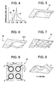
- FIG. 4 is a graph of impedance versus driving frequencies for a TFR test sample.
- FIGS. 5-7 are three-dimensional mapped views of vibrational modes of the TFR test sample corresponding to the frequencies in the graph of FIG. 4 .
- FIG. 8 is a schematic diagram of a micro-electro-mechanical system (MEMS) four-drumhead resonator test sample.
- MEMS micro-electro-mechanical system
- FIGS. 9-11 are three-dimensional mapped views of vibrational modes of the MEMS test sample of FIG. 8 corresponding to various driving frequencies.
- FIG. 12 is a schematic diagram of a piezoelectric crystal test sample having traveling surface acoustic waves thereon.
- FIGS. 13-15 are three-dimensional mapped views of the traveling surface acoustic waves of the piezoelectric crystal of FIG. 12 taken at various locations on a surface thereof.
- the apparatus includes a signal source 32 for driving the electro-acoustic device 31 to produce at least one vibrational mode therein.
- An optical interferometer 33 collects phase and amplitude data from the electro-acoustic device 31 .
- a controller 34 is coupled to the signal source 32 and the optical interferometer 33 for controlling the signal source and mapping the at least one vibrational mode based upon the collected phase and amplitude data, as will be discussed in further detail below.
- the optical interferometer 33 may include an optical detector 38 providing an output signal.
- the controller 34 preferably homodynes the output signal from the optical detector and phase-detects the homodyned output signal to determine the phase and amplitude data. Furthermore, the controller may phaseshift the homodyned output signal prior to phasedetecting to increase signal amplitude.
- the optical interferometer 33 includes at least one light source, such as a HeNe laser 39 for directing a sample light beam 40 at the electroacoustic device 31 and for providing a reference light beam 41 .
- the reference light beam 41 may be produced using a beamsplitter 42 , as discussed further below, and the optical detector 38 may be used for comparing the reflected light beam 40 and the reference light beam to determine the phase and amplitude data.
- a sensitivity value relating to an alignment error between the reference light beam 41 and the sample light beam 40 may therefore be determined, and the amplitude data may be normalized using the sensitivity value.
- the controller 34 may plot the phase and amplitude data to provide an instantaneous three-dimensional view of the at least one vibrational mode. Moreover, the controller 34 may construct a sequence of instantaneous three-dimensional views to form a motion picture of the at least one vibrational mode. The mapped at least one vibrational mode may be displayed on a display 35 coupled to the controller 34 . Furthermore, a raster scanner 36 may be provided for stepping the sample 31 to provide phase and amplitude data across a surface of the sample.
- the optical scanning interferometer 33 may be a standard Michelson interferometer with a tightly focused sample beam and a high speed photodetector 38 on the recombined output beams, for example.
- a feedback system maintains the interference pattern on a single fringe at its maximum sensitivity to sample motion. Variations in the output voltage due to vibrations at a sample frequency may be homodyned and phase-detected at a lower frequency to provide both the amplitude of the motion and its phase relative to the exciting voltage applied to the device.
- the sample 31 is stepped (using x-y motors) with the raster scanner 36 . At each point, amplitude and phase data are recorded and later combined to provide a snapshot in time of the surface.
- the lateral resolution (dx, dy) is determined by a spot size S of the sample light beam 41 on the sample 31 , which may be about 1 ⁇ m, for example.
- the vertical resolution dz may be six to seven orders of magnitude better, i.e., 0.001-0.01 ⁇ . Due to the vibrational noise introduced by the motorized translation stages of the raster scanner 36 , the data is preferably collected while the sample 31 is not being moved. After each step, therefore, a pause of one second, for example, allows the system to recover from the motion before data is taken. As such, a typical data collection rate may be about 3000 points/hour, for example.
- the magnitude and phase of the signal may be recorded, along with a third variable proportional to the interferometer sensitivity.
- This third variable is used to normalize the magnitude data, thus taking into account, for example, any variations in reflectivity or degree of focus over the surface of the sample.
- a Faraday isolator 43 may be used to provide approximately 40 dB discrimination (e.g., about 40 dB) against light reflected back into the laser by a mirror 52 , and the combination of a pinhole 44 and lenses 45 and 46 provides beam expansion (e.g., ⁇ 6) and spatial filtering.
- the beamsplitter 42 which may be non-polarized, for example, divides the beam equally into the reference light beam 41 and the sample light beam 40 .
- the reference light beam 41 is reflected from a mirror 47 mounted on a piezoelectric stack (PES) 48 capable of 15 ⁇ m of movement for 150 applied volts, which is used for stabilization and calibration.
- the reflected sample light beam 40 combines with the reflected reference light beam 41 and is focused by a lens 50 to a diameter waist (e.g., 20 ⁇ m) to fit within the active area of the optical detector 38 .
- a diameter waist e.g. 20 ⁇ m
- One example of an optical detector 38 is an InGaAs Schottky photodiode which has about a 25 ⁇ m active area diameter.
- the optical detector 38 is sensitive over a wide bandwidth (e.g., 10 kHz-6 GHz) for the Schottky photodiode and it is also preferably equipped with a bias current monitor 51 providing a separate, low-frequency signal (0-50 kHz).
- a wide bandwidth e.g. 10 kHz-6 GHz
- a bias current monitor 51 providing a separate, low-frequency signal (0-50 kHz).
- the bias current monitor 51 may be used to monitor a response function of the interferometer 33 , which is illustratively shown in FIG. 3 .
- PSD phase sensitive detection
- PSD at 2 f m provides a signal which can be fed back to the PES 48 as an error signal to lock the interferometer 33 onto one of the operating points (illustratively shown with arrows in FIG. 3) corresponding to a maximum sensitivity dI/d ⁇ .
- Sensitivity of the interferometer 33 to small movements of either the sample 31 or the reference mirror 47 is given by the slope of the interferometer response function.
- the low-frequency bias-current monitor 51 of the optical detector 33 is used to detect the 1 kHz signal which is then fed to each of two phase sensitive detectors 53 , 54 , one being tuned to fm and the other to 2 f m .
- the 2 f m signal is proportional to the second derivative of the interferometer response function and can be used as the error signal in a feedback system, i.e., integrated electronically and fed back to the stack as a low-frequency quasi-DC control signal added to the modulating signal at f m .
- the interferometer 33 is therefore maintained at a position of highest sensitivity, indicated by the arrows in FIG. 3 .
- the sign of the feedback voltage determines which positions are stable (odd or even multiples of p).
- phase sensitive detector 54 tuned to f m provides a measure of the slope of the interferometer response function, i.e., its sensitivity.
- the sample 31 may be an interdigital transducer on a piezoelectric material (i.e., SAW devices) or other transducers such as magnetostrictive, electrostrictive, or electromagnetic acoustic transducers, a surface piezoelectric capacitor (i.e., thin film resonators), or other elecrostatically-activated samples (e.g., MEMS-type) known to those of skill in the art.
- SAW devices piezoelectric material
- other transducers such as magnetostrictive, electrostrictive, or electromagnetic acoustic transducers, a surface piezoelectric capacitor (i.e., thin film resonators), or other elecrostatically-activated samples (e.g., MEMS-type) known to those of skill in the art.
- MEMS-type elecrostatically-activated samples
- the RF voltage may be amplitude modulated at a frequency lower than the driving frequency (e.g., 50 kHz) by an audio source 55 for later discrimination against noise and applied to the sample 31 at the driving frequency.
- the driving frequencies may be close to or at a resonant frequency of the sample 31 .
- the amplified high-frequency output of the optical detector 38 may be homodyned to zero frequency by mixing with the unmodulated RF carrier and phase-shifted to produce maximum signal amplitude, as will be appreciated by those of skill in the art.
- the resulting sideband at 50 kHz may then be phase-detected by a lock-in amplifier, providing both the amplitude (M) and the phase ( ⁇ ) of the oscillatory signal, as shown in FIG. 2 .
- An RF mixer 56 and a 50 kHz phase sensitive detector 57 operate by taking products of sinusoidal waves such as A 1 sin( 107 1 t+ ⁇ 1 )A 2 sin( ⁇ 2 t+ ⁇ 2 ), resulting in terms like A 1 A 2 sin(( ⁇ 1 ⁇ 2 )t+ ⁇ 1 ⁇ 2 ).
- the phase of the gigahertz response of the interferometer is carried through to the phase output of the 50 kHz lock-in amplifier. While the absolute value of the phase is not useful, the relative phase from one point to another on the sample represents the true relative RF phase.
- Data are collected by the controller 34 by stepping the sample 31 in the raster scanner 36 with respect to the interferometer focal point using x and y motors, which typically have a resolution of about 0.1 ⁇ m.
- the controller 33 may be a computer or a network analyzer, for example, such as the HP 8712 and 8714 series network analyzers from Hewlett-Packard Co., Palo Alto, Calif. After each step, a pause of 1 second may be imposed to allow the control system and data signals to recover from the vibrationally induced noise of the step, as discussed above.
- the data collected at each step may include three numbers, namely the magnitude and phase of the 50 kHz signal and the magnitude of the f m signal from the PSD tuned to f m .
- the latter is used to monitor the sensitivity of the interferometer and may be used to correct the magnitude of the main signal for changes in the sensitivity due, for example, to changes in the reflectivity of the surface.
- the f m signal may also be used to construct a microscope-like image of the electrodes.
- the lateral resolution on the surface of the sample is dependent upon the spot size S.
- S is usually defined as the diameter within which most (86%) of the light falls: 4 ⁇ op F/ ⁇ D, where ⁇ op is the laser wavelength, F is the focal length of the objective, and D is the diameter of the beam incident on the objective.
- Both the surface of the sample 31 and the translation axes may be perpendicular to the beam direction to ensure that the sample (which is assumed to be flat) is in focus over the entire scanned area.
- Typical misalignment may be held to less than about 0.1° according to the present invention using the above described components.
- the vertical resolution, perpendicular to the surface, will typically be more than six orders of magnitude smaller than the lateral resolution.
- the sensitivity of the interferometer 33 ⁇ I/ ⁇ z, can be maximized by using a laser intensity equal to the maximum allowable intensity for the particular detector used (3 mW for linear operation, for example).
- the maximum net optical power through the beamsplitter 42 to the optical detector 38 is half the laser power, and the operating point is at half the maximum safe power in the optical detector (e.g., about 6 mW).
- NEP noise equivalent power
- the interferometer 33 may be constructed as rigidly and compactly as possible using standard optical components and mounts.
- the reference mirror 47 and the sample 31 may be positioned to have substantially equal optical path lengths from the beamsplitter 42 , e.g., within about 1 mm.
- Tubes e.g., 6 mm ID
- Further precautions may include using two stages of vibration isolation to decouple the interferometer from floor vibrations.
- a padded wooden box or the like over the interferometer may be used to shield against ambient acoustic and optical noise.
- laboratory air-conditioning fans may be turned off during data collection.
- FIGS. 4-6 illustrations of various vibrational modes mapped in accordance with the present invention may be seen.
- Driving frequencies 65 - 67 used to produce vibrational modes in a TFR are shown with dotted lines in the graph of FIG. 4 which illustrates impedance at the various frequencies.
- the TFR generates enhanced vertical motion at the drive frequency for which the thickness of the piezoelectric layer (e.g., a 2.75 ⁇ m layer of AlN) is just half an acoustic wavelength.
- the driving frequency 65 of 1.75 GHz i.e., resonance zero
- this produces a uniform up and down pancake mode (FIG. 6 )
- the mode pattern is much more complicated (FIGS. 7 and 8, respectively).
- the phase information is particularly important for obtaining the correct instantaneous surface shape.
- the average in-plane wavelength observed for the above TFR varies smoothly with frequency in a way that can be understood by treating the photoelectric layer as an acoustic waveguide, as will be appreciated by those of skill in the art.
- Motion pictures at the above three frequencies show this behavior clearly and also demonstrate that the waves are standing waves.
- Other standing-wave patterns, with wavelengths in the 2-5 ⁇ m range, are observable, especially in scans with a smaller step size.
- Fourier analysis of what appears to be noise away from the electrode reveals discrete propagation vectors with random orientation in the plane.
- Calculation of the dispersion curves for the allowed modes in this layered structure serve to identify the observed modes as Lamb modes (10-50 ⁇ m wavelength) and surface acoustic waves (2-5 ⁇ m wavelength). Measurement of the mode structure is important for understanding and improving the electro-mechanical response of this piezoelectric system.
- Maps of the data for a micro-electro-mechanical system (MEMS) four-drumhead resonator 60 may be seen in FIGS. 9-11.
- Each drumhead may be formed by etching away a portion of a sacrificial layer through an access hole in a top layer, for example. The etching is allowed to continue long enough that the circular drumheads overlap slightly and are therefore coupled to each other mechanically.
- One drumhead is driven electrically, as described above, with a single-polarity RF voltage applied to an Au ring electrode thereof, generating an electrostatic RF attraction to a grounded, doped Si substrate. The coupling between drumheads results in three vibrational modes at the frequencies shown, with obvious phase relationships.
- phase pattern observed at the lowest-frequency resonance where all of the drumheads are in phase implies that the mode-determining coupling parameter is the strain, not the bending, of the drumhead material in the overlap region. If bending were dominant, the vibrational mode shown in FIG. 9 should have the highest resonant frequency instead of the lowest. The identification of such mode structures would clearly be impossible using prior art methods which do not provide phase information, as does the present invention.
- the data may be taken through the window of a small vacuum chamber with a partial pressure of air such that a quality factor, or Q, at each resonance is approximately 150 . This is low enough to cause additional small phase shifts (besides the obvious 0° or 180° C.) between the driven drumhead and the remaining drumheads, which can be observed readily in the motion pictures of the data.
- FIGS. 13-15 Data for traveling surface acoustic waves on a piezoelectric crystal 61 (shown in FIG. 12) may be seen in FIGS. 13-15.
- the waves were generated by applying an RF voltage to an interdigital transducer, as part of a Sawtek filter centered at 170 MHZ with a bandwidth of 1.2 MHZ.
- the data was taken at three locations 62 , 63 and 64 on the bare crystal (corresponding to FIGS. 13, 14 , and 15 , respectively), approximately 3 mm away from the 1 mm aperture interdigital transducer.
- One scan at location 63 is in the direct path of the acoustic beam, while the other two locations 62 , 64 are to either side of the beam, in regions where waves exist only because of beam spreading by acoustic diffraction.
- the wavefronts in locations 62 , 64 are no longer straight lines across the beam, i.e., the edges lag behind the central beam as expected for diffraction. It is clear from the motion picture that this is a wave traveling to the right, rather than a standing wave. Without phase information as provided by the present invention, a traveling wave would look instead like the pancake mode described with reference to FIG. 5 above.
- the general technique described herein may be applied in many areas of science and technology where vibrations of a surface are important. According to the present invention, one gains not only a high-resolution quantitative measurement but also a deeper intuitive understanding of the vibrational modes, as the slow-motion pictures bring the high-frequency motion into the range of human experience.
- the exemplary vertical resolution described above could be increased by 1-2 orders of magnitude (or more) by using a more intense laser and even better isolation from room vibrations.
- the lateral resolution could be improved by a factor of 10 or more, for example, using near-field optical scanning, as will be appreciated by those of skill in the art. Operation at elevated or reduced sample temperature is possible, and yet higher-frequency optical detectors are also available. None of these extensions would sacrifice the important phase information, which enables accurate and dynamic visualization of these minute vibrational modes.
Abstract
Description
Claims (28)
Priority Applications (1)
| Application Number | Priority Date | Filing Date | Title |
|---|---|---|---|
| US09/702,713 US6587212B1 (en) | 2000-10-31 | 2000-10-31 | Method and apparatus for studying vibrational modes of an electro-acoustic device |
Applications Claiming Priority (1)
| Application Number | Priority Date | Filing Date | Title |
|---|---|---|---|
| US09/702,713 US6587212B1 (en) | 2000-10-31 | 2000-10-31 | Method and apparatus for studying vibrational modes of an electro-acoustic device |
Publications (1)
| Publication Number | Publication Date |
|---|---|
| US6587212B1 true US6587212B1 (en) | 2003-07-01 |
Family
ID=24822306
Family Applications (1)
| Application Number | Title | Priority Date | Filing Date |
|---|---|---|---|
| US09/702,713 Expired - Fee Related US6587212B1 (en) | 2000-10-31 | 2000-10-31 | Method and apparatus for studying vibrational modes of an electro-acoustic device |
Country Status (1)
| Country | Link |
|---|---|
| US (1) | US6587212B1 (en) |
Cited By (10)
| Publication number | Priority date | Publication date | Assignee | Title |
|---|---|---|---|---|
| US20030037616A1 (en) * | 2000-03-24 | 2003-02-27 | Eiolf Vikhagen | Method for vibration measurement and interferometer |
| US6753528B1 (en) * | 2002-04-18 | 2004-06-22 | Kla-Tencor Technologies Corporation | System for MEMS inspection and characterization |
| US20050280830A1 (en) * | 2004-06-22 | 2005-12-22 | Polytec Gmbh | Apparatus for optical measurement of an object |
| JP2008003597A (en) * | 2006-06-19 | 2008-01-10 | Polytec Gmbh | Scanning microscope for optically measuring an object |
| US20090079521A1 (en) * | 2005-12-02 | 2009-03-26 | Habbo Heinze | Bulk Acoustic Wave Resonator |
| US20090315889A1 (en) * | 2005-07-18 | 2009-12-24 | Diego Giuseppe Tognola | Signal process and system |
| US20100118313A1 (en) * | 2008-11-12 | 2010-05-13 | Deck Leslie L | Phase-shifting interferometry in the presence of vibration |
| WO2010121846A1 (en) | 2009-04-23 | 2010-10-28 | Femtotools Gmbh | Method and inspection system for testing of micro fabricated structures |
| US20170122721A1 (en) * | 2014-08-28 | 2017-05-04 | Shenzhen Orbbec Co., Ltd. | Overall z-direction displacement measuring system |
| CN111521566A (en) * | 2020-06-09 | 2020-08-11 | 中国计量科学研究院 | Laser ultrasonic nondestructive testing system based on double-wave mixing |
Citations (56)
| Publication number | Priority date | Publication date | Assignee | Title |
|---|---|---|---|---|
| US4502932A (en) | 1983-10-13 | 1985-03-05 | The United States Of America As Represented By The United States Department Of Energy | Acoustic resonator and method of making same |
| US4556812A (en) | 1983-10-13 | 1985-12-03 | The United States Of America As Represented By The United States Department Of Energy | Acoustic resonator with Al electrodes on an AlN layer and using a GaAs substrate |
| US4719383A (en) | 1985-05-20 | 1988-01-12 | The United States Of America As Represented By The United States Department Of Energy | Piezoelectric shear wave resonator and method of making same |
| US4890370A (en) | 1987-10-09 | 1990-01-02 | Murata Manufacturing Co., Ltd. | Manufacturing method for integrated resonator |
| US4928527A (en) * | 1988-04-29 | 1990-05-29 | At&T Bell Laboratories | Method and device for nondestructive evaluation |
| US4988957A (en) | 1989-05-26 | 1991-01-29 | Iowa State University Research Foundation, Inc. | Electronically-tuned thin-film resonator/filter controlled oscillator |
| US5075641A (en) | 1990-12-04 | 1991-12-24 | Iowa State University Research Foundation, Inc. | High frequency oscillator comprising cointegrated thin film resonator and active device |
| US5166646A (en) | 1992-02-07 | 1992-11-24 | Motorola, Inc. | Integrated tunable resonators for use in oscillators and filters |
| US5185589A (en) | 1991-05-17 | 1993-02-09 | Westinghouse Electric Corp. | Microwave film bulk acoustic resonator and manifolded filter bank |
| US5231327A (en) | 1990-12-14 | 1993-07-27 | Tfr Technologies, Inc. | Optimized piezoelectric resonator-based networks |
| US5233259A (en) | 1991-02-19 | 1993-08-03 | Westinghouse Electric Corp. | Lateral field FBAR |
| US5232571A (en) | 1991-12-23 | 1993-08-03 | Iowa State University Research Foundation, Inc. | Aluminum nitride deposition using an AlN/Al sputter cycle technique |
| US5283458A (en) | 1992-03-30 | 1994-02-01 | Trw Inc. | Temperature stable semiconductor bulk acoustic resonator |
| US5291159A (en) | 1992-07-20 | 1994-03-01 | Westinghouse Electric Corp. | Acoustic resonator filter with electrically variable center frequency and bandwidth |
| US5294898A (en) | 1992-01-29 | 1994-03-15 | Motorola, Inc. | Wide bandwidth bandpass filter comprising parallel connected piezoelectric resonators |
| US5303457A (en) | 1991-02-04 | 1994-04-19 | Motorola, Inc. | Method for packaging microelectronic frequency selection components |
| US5334960A (en) | 1993-02-16 | 1994-08-02 | Motorola, Inc. | Conjugately matched acoustic wave transducers and method |
| US5348617A (en) | 1991-12-23 | 1994-09-20 | Iowa State University Research Foundation, Inc. | Selective etching process |
| US5367308A (en) | 1992-05-29 | 1994-11-22 | Iowa State University Research Foundation, Inc. | Thin film resonating device |
| US5373268A (en) | 1993-02-01 | 1994-12-13 | Motorola, Inc. | Thin film resonator having stacked acoustic reflecting impedance matching layers and method |
| US5381385A (en) | 1993-08-04 | 1995-01-10 | Hewlett-Packard Company | Electrical interconnect for multilayer transducer elements of a two-dimensional transducer array |
| US5403701A (en) | 1991-12-13 | 1995-04-04 | Hewlett-Packard Company | Method of forming small geometry patterns on piezoelectric membrane films |
| US5438554A (en) | 1993-06-15 | 1995-08-01 | Hewlett-Packard Company | Tunable acoustic resonator for clinical ultrasonic transducers |
| US5446306A (en) | 1993-12-13 | 1995-08-29 | Trw Inc. | Thin film voltage-tuned semiconductor bulk acoustic resonator (SBAR) |
| US5552655A (en) | 1994-05-04 | 1996-09-03 | Trw Inc. | Low frequency mechanical resonator |
| US5587620A (en) | 1993-12-21 | 1996-12-24 | Hewlett-Packard Company | Tunable thin film acoustic resonators and method for making the same |
| US5596239A (en) | 1995-06-29 | 1997-01-21 | Motorola, Inc. | Enhanced quality factor resonator |
| US5617065A (en) | 1995-06-29 | 1997-04-01 | Motorola, Inc. | Filter using enhanced quality factor resonator and method |
| US5630949A (en) | 1995-06-01 | 1997-05-20 | Tfr Technologies, Inc. | Method and apparatus for fabricating a piezoelectric resonator to a resonant frequency |
| US5646583A (en) | 1996-01-04 | 1997-07-08 | Rockwell International Corporation | Acoustic isolator having a high impedance layer of hafnium oxide |
| US5692279A (en) | 1995-08-17 | 1997-12-02 | Motorola | Method of making a monolithic thin film resonator lattice filter |
| US5698928A (en) | 1995-08-17 | 1997-12-16 | Motorola, Inc. | Thin film piezoelectric arrays with enhanced coupling and fabrication methods |
| US5702775A (en) | 1995-12-26 | 1997-12-30 | Motorola, Inc. | Microelectronic device package and method |
| US5714917A (en) | 1996-10-02 | 1998-02-03 | Nokia Mobile Phones Limited | Device incorporating a tunable thin film bulk acoustic resonator for performing amplitude and phase modulation |
| US5760663A (en) | 1996-08-23 | 1998-06-02 | Motorola, Inc. | Elliptic baw resonator filter and method of making the same |
| US5780713A (en) | 1996-11-19 | 1998-07-14 | Hewlett-Packard Company | Post-fabrication tuning of acoustic resonators |
| US5789845A (en) | 1994-11-24 | 1998-08-04 | Mitsubishi Denki Kabushiki Kaisha | Film bulk acoustic wave device |
| US5821833A (en) | 1995-12-26 | 1998-10-13 | Tfr Technologies, Inc. | Stacked crystal filter device and method of making |
| US5853601A (en) | 1997-04-03 | 1998-12-29 | Northrop Grumman Corporation | Top-via etch technique for forming dielectric membranes |
| US5864261A (en) | 1994-05-23 | 1999-01-26 | Iowa State University Research Foundation | Multiple layer acoustical structures for thin-film resonator based circuits and systems |
| US5872493A (en) | 1997-03-13 | 1999-02-16 | Nokia Mobile Phones, Ltd. | Bulk acoustic wave (BAW) filter having a top portion that includes a protective acoustic mirror |
| US5873154A (en) | 1996-10-17 | 1999-02-23 | Nokia Mobile Phones Limited | Method for fabricating a resonator having an acoustic mirror |
| US5883575A (en) | 1997-08-12 | 1999-03-16 | Hewlett-Packard Company | RF-tags utilizing thin film bulk wave acoustic resonators |
| US5894647A (en) | 1997-06-30 | 1999-04-20 | Tfr Technologies, Inc. | Method for fabricating piezoelectric resonators and product |
| US5910756A (en) | 1997-05-21 | 1999-06-08 | Nokia Mobile Phones Limited | Filters and duplexers utilizing thin film stacked crystal filter structures and thin film bulk acoustic wave resonators |
| US5942958A (en) | 1998-07-27 | 1999-08-24 | Tfr Technologies, Inc. | Symmetrical piezoelectric resonator filter |
| US5963856A (en) | 1997-01-03 | 1999-10-05 | Lucent Technologies Inc | Wireless receiver including tunable RF bandpass filter |
| US6051907A (en) | 1996-10-10 | 2000-04-18 | Nokia Mobile Phones Limited | Method for performing on-wafer tuning of thin film bulk acoustic wave resonators (FBARS) |
| US6060818A (en) | 1998-06-02 | 2000-05-09 | Hewlett-Packard Company | SBAR structures and method of fabrication of SBAR.FBAR film processing techniques for the manufacturing of SBAR/BAR filters |
| US6081171A (en) | 1998-04-08 | 2000-06-27 | Nokia Mobile Phones Limited | Monolithic filters utilizing thin film bulk acoustic wave devices and minimum passive components for controlling the shape and width of a passband response |
| US6087198A (en) | 1998-02-12 | 2000-07-11 | Texas Instruments Incorporated | Low cost packaging for thin-film resonators and thin-film resonator-based filters |
| US6127768A (en) | 1997-05-09 | 2000-10-03 | Kobe Steel Usa, Inc. | Surface acoustic wave and bulk acoustic wave devices using a Zn.sub.(1-X) Yx O piezoelectric layer device |
| US6150703A (en) | 1998-06-29 | 2000-11-21 | Trw Inc. | Lateral mode suppression in semiconductor bulk acoustic resonator (SBAR) devices using tapered electrodes, and electrodes edge damping materials |
| US6198208B1 (en) | 1999-05-20 | 2001-03-06 | Tdk Corporation | Thin film piezoelectric device |
| US6204737B1 (en) | 1998-06-02 | 2001-03-20 | Nokia Mobile Phones, Ltd | Piezoelectric resonator structures with a bending element performing a voltage controlled switching function |
| US6215375B1 (en) | 1999-03-30 | 2001-04-10 | Agilent Technologies, Inc. | Bulk acoustic wave resonator with improved lateral mode suppression |
-
2000
- 2000-10-31 US US09/702,713 patent/US6587212B1/en not_active Expired - Fee Related
Patent Citations (60)
| Publication number | Priority date | Publication date | Assignee | Title |
|---|---|---|---|---|
| US4556812A (en) | 1983-10-13 | 1985-12-03 | The United States Of America As Represented By The United States Department Of Energy | Acoustic resonator with Al electrodes on an AlN layer and using a GaAs substrate |
| US4502932A (en) | 1983-10-13 | 1985-03-05 | The United States Of America As Represented By The United States Department Of Energy | Acoustic resonator and method of making same |
| US4719383A (en) | 1985-05-20 | 1988-01-12 | The United States Of America As Represented By The United States Department Of Energy | Piezoelectric shear wave resonator and method of making same |
| US4890370A (en) | 1987-10-09 | 1990-01-02 | Murata Manufacturing Co., Ltd. | Manufacturing method for integrated resonator |
| US4928527A (en) * | 1988-04-29 | 1990-05-29 | At&T Bell Laboratories | Method and device for nondestructive evaluation |
| US4988957A (en) | 1989-05-26 | 1991-01-29 | Iowa State University Research Foundation, Inc. | Electronically-tuned thin-film resonator/filter controlled oscillator |
| US5075641A (en) | 1990-12-04 | 1991-12-24 | Iowa State University Research Foundation, Inc. | High frequency oscillator comprising cointegrated thin film resonator and active device |
| US5231327A (en) | 1990-12-14 | 1993-07-27 | Tfr Technologies, Inc. | Optimized piezoelectric resonator-based networks |
| US5404628A (en) | 1990-12-14 | 1995-04-11 | Tfr Technologies, Inc. | Method for optimizing piezoelectric resonator-based networks |
| US5303457A (en) | 1991-02-04 | 1994-04-19 | Motorola, Inc. | Method for packaging microelectronic frequency selection components |
| US5233259A (en) | 1991-02-19 | 1993-08-03 | Westinghouse Electric Corp. | Lateral field FBAR |
| US5185589A (en) | 1991-05-17 | 1993-02-09 | Westinghouse Electric Corp. | Microwave film bulk acoustic resonator and manifolded filter bank |
| US5403701A (en) | 1991-12-13 | 1995-04-04 | Hewlett-Packard Company | Method of forming small geometry patterns on piezoelectric membrane films |
| US5232571A (en) | 1991-12-23 | 1993-08-03 | Iowa State University Research Foundation, Inc. | Aluminum nitride deposition using an AlN/Al sputter cycle technique |
| US5348617A (en) | 1991-12-23 | 1994-09-20 | Iowa State University Research Foundation, Inc. | Selective etching process |
| US5294898A (en) | 1992-01-29 | 1994-03-15 | Motorola, Inc. | Wide bandwidth bandpass filter comprising parallel connected piezoelectric resonators |
| US5166646A (en) | 1992-02-07 | 1992-11-24 | Motorola, Inc. | Integrated tunable resonators for use in oscillators and filters |
| US5283458A (en) | 1992-03-30 | 1994-02-01 | Trw Inc. | Temperature stable semiconductor bulk acoustic resonator |
| US5367308A (en) | 1992-05-29 | 1994-11-22 | Iowa State University Research Foundation, Inc. | Thin film resonating device |
| US5291159A (en) | 1992-07-20 | 1994-03-01 | Westinghouse Electric Corp. | Acoustic resonator filter with electrically variable center frequency and bandwidth |
| US5373268A (en) | 1993-02-01 | 1994-12-13 | Motorola, Inc. | Thin film resonator having stacked acoustic reflecting impedance matching layers and method |
| US5334960A (en) | 1993-02-16 | 1994-08-02 | Motorola, Inc. | Conjugately matched acoustic wave transducers and method |
| US5438554A (en) | 1993-06-15 | 1995-08-01 | Hewlett-Packard Company | Tunable acoustic resonator for clinical ultrasonic transducers |
| US5381385A (en) | 1993-08-04 | 1995-01-10 | Hewlett-Packard Company | Electrical interconnect for multilayer transducer elements of a two-dimensional transducer array |
| US5446306A (en) | 1993-12-13 | 1995-08-29 | Trw Inc. | Thin film voltage-tuned semiconductor bulk acoustic resonator (SBAR) |
| US5587620A (en) | 1993-12-21 | 1996-12-24 | Hewlett-Packard Company | Tunable thin film acoustic resonators and method for making the same |
| US5873153A (en) | 1993-12-21 | 1999-02-23 | Hewlett-Packard Company | Method of making tunable thin film acoustic resonators |
| US5552655A (en) | 1994-05-04 | 1996-09-03 | Trw Inc. | Low frequency mechanical resonator |
| US5864261A (en) | 1994-05-23 | 1999-01-26 | Iowa State University Research Foundation | Multiple layer acoustical structures for thin-film resonator based circuits and systems |
| US5789845A (en) | 1994-11-24 | 1998-08-04 | Mitsubishi Denki Kabushiki Kaisha | Film bulk acoustic wave device |
| US5630949A (en) | 1995-06-01 | 1997-05-20 | Tfr Technologies, Inc. | Method and apparatus for fabricating a piezoelectric resonator to a resonant frequency |
| US5596239A (en) | 1995-06-29 | 1997-01-21 | Motorola, Inc. | Enhanced quality factor resonator |
| US5617065A (en) | 1995-06-29 | 1997-04-01 | Motorola, Inc. | Filter using enhanced quality factor resonator and method |
| US5884378A (en) | 1995-06-29 | 1999-03-23 | Motorola, Inc. | Method of making an enhanced quality factor resonator |
| US5692279A (en) | 1995-08-17 | 1997-12-02 | Motorola | Method of making a monolithic thin film resonator lattice filter |
| US5698928A (en) | 1995-08-17 | 1997-12-16 | Motorola, Inc. | Thin film piezoelectric arrays with enhanced coupling and fabrication methods |
| US5821833A (en) | 1995-12-26 | 1998-10-13 | Tfr Technologies, Inc. | Stacked crystal filter device and method of making |
| US5928598A (en) | 1995-12-26 | 1999-07-27 | Motorola, Inc. | Method of making a microelectronic device package |
| US5702775A (en) | 1995-12-26 | 1997-12-30 | Motorola, Inc. | Microelectronic device package and method |
| US5646583A (en) | 1996-01-04 | 1997-07-08 | Rockwell International Corporation | Acoustic isolator having a high impedance layer of hafnium oxide |
| US5760663A (en) | 1996-08-23 | 1998-06-02 | Motorola, Inc. | Elliptic baw resonator filter and method of making the same |
| US5714917A (en) | 1996-10-02 | 1998-02-03 | Nokia Mobile Phones Limited | Device incorporating a tunable thin film bulk acoustic resonator for performing amplitude and phase modulation |
| US6051907A (en) | 1996-10-10 | 2000-04-18 | Nokia Mobile Phones Limited | Method for performing on-wafer tuning of thin film bulk acoustic wave resonators (FBARS) |
| US5873154A (en) | 1996-10-17 | 1999-02-23 | Nokia Mobile Phones Limited | Method for fabricating a resonator having an acoustic mirror |
| US5780713A (en) | 1996-11-19 | 1998-07-14 | Hewlett-Packard Company | Post-fabrication tuning of acoustic resonators |
| US5963856A (en) | 1997-01-03 | 1999-10-05 | Lucent Technologies Inc | Wireless receiver including tunable RF bandpass filter |
| US5872493A (en) | 1997-03-13 | 1999-02-16 | Nokia Mobile Phones, Ltd. | Bulk acoustic wave (BAW) filter having a top portion that includes a protective acoustic mirror |
| US5853601A (en) | 1997-04-03 | 1998-12-29 | Northrop Grumman Corporation | Top-via etch technique for forming dielectric membranes |
| US6127768A (en) | 1997-05-09 | 2000-10-03 | Kobe Steel Usa, Inc. | Surface acoustic wave and bulk acoustic wave devices using a Zn.sub.(1-X) Yx O piezoelectric layer device |
| US5910756A (en) | 1997-05-21 | 1999-06-08 | Nokia Mobile Phones Limited | Filters and duplexers utilizing thin film stacked crystal filter structures and thin film bulk acoustic wave resonators |
| US5894647A (en) | 1997-06-30 | 1999-04-20 | Tfr Technologies, Inc. | Method for fabricating piezoelectric resonators and product |
| US5883575A (en) | 1997-08-12 | 1999-03-16 | Hewlett-Packard Company | RF-tags utilizing thin film bulk wave acoustic resonators |
| US6087198A (en) | 1998-02-12 | 2000-07-11 | Texas Instruments Incorporated | Low cost packaging for thin-film resonators and thin-film resonator-based filters |
| US6081171A (en) | 1998-04-08 | 2000-06-27 | Nokia Mobile Phones Limited | Monolithic filters utilizing thin film bulk acoustic wave devices and minimum passive components for controlling the shape and width of a passband response |
| US6060818A (en) | 1998-06-02 | 2000-05-09 | Hewlett-Packard Company | SBAR structures and method of fabrication of SBAR.FBAR film processing techniques for the manufacturing of SBAR/BAR filters |
| US6204737B1 (en) | 1998-06-02 | 2001-03-20 | Nokia Mobile Phones, Ltd | Piezoelectric resonator structures with a bending element performing a voltage controlled switching function |
| US6150703A (en) | 1998-06-29 | 2000-11-21 | Trw Inc. | Lateral mode suppression in semiconductor bulk acoustic resonator (SBAR) devices using tapered electrodes, and electrodes edge damping materials |
| US5942958A (en) | 1998-07-27 | 1999-08-24 | Tfr Technologies, Inc. | Symmetrical piezoelectric resonator filter |
| US6215375B1 (en) | 1999-03-30 | 2001-04-10 | Agilent Technologies, Inc. | Bulk acoustic wave resonator with improved lateral mode suppression |
| US6198208B1 (en) | 1999-05-20 | 2001-03-06 | Tdk Corporation | Thin film piezoelectric device |
Non-Patent Citations (1)
| Title |
|---|
| Engan, H., Phase Sensitive Laser Probe for High-Frequency Surface Acoustic Wave Measurementsvol. SU-25, No. 6, Nov. 1978, p. 372-377. |
Cited By (19)
| Publication number | Priority date | Publication date | Assignee | Title |
|---|---|---|---|---|
| US6970251B2 (en) * | 2000-03-24 | 2005-11-29 | Optonor As | Method for vibration measurement and interferometer |
| US20030037616A1 (en) * | 2000-03-24 | 2003-02-27 | Eiolf Vikhagen | Method for vibration measurement and interferometer |
| US6753528B1 (en) * | 2002-04-18 | 2004-06-22 | Kla-Tencor Technologies Corporation | System for MEMS inspection and characterization |
| US20050280830A1 (en) * | 2004-06-22 | 2005-12-22 | Polytec Gmbh | Apparatus for optical measurement of an object |
| US7443513B2 (en) * | 2004-06-22 | 2008-10-28 | Polytec Gmbh | Apparatus for optical measurement of an object |
| US20090315889A1 (en) * | 2005-07-18 | 2009-12-24 | Diego Giuseppe Tognola | Signal process and system |
| US8089349B2 (en) * | 2005-07-18 | 2012-01-03 | Diego Giuseppe Tognola | Signal process and system |
| US7961066B2 (en) | 2005-12-02 | 2011-06-14 | Epcos Ag | Bulk acoustic wave resonator filter |
| US20090079521A1 (en) * | 2005-12-02 | 2009-03-26 | Habbo Heinze | Bulk Acoustic Wave Resonator |
| JP2008003597A (en) * | 2006-06-19 | 2008-01-10 | Polytec Gmbh | Scanning microscope for optically measuring an object |
| US20100118313A1 (en) * | 2008-11-12 | 2010-05-13 | Deck Leslie L | Phase-shifting interferometry in the presence of vibration |
| US20110026036A1 (en) * | 2008-11-12 | 2011-02-03 | Deck Leslie L | Phase-shifting interferometry in the presence of vibration |
| US7948639B2 (en) | 2008-11-12 | 2011-05-24 | Zygo Corporation | Phase-shifting interferometry in the presence of vibration |
| US7796273B2 (en) * | 2008-11-12 | 2010-09-14 | Zygo Corporation | Phase-shifting interferometry in the presence of vibration |
| WO2010121846A1 (en) | 2009-04-23 | 2010-10-28 | Femtotools Gmbh | Method and inspection system for testing of micro fabricated structures |
| US20170122721A1 (en) * | 2014-08-28 | 2017-05-04 | Shenzhen Orbbec Co., Ltd. | Overall z-direction displacement measuring system |
| US10234264B2 (en) * | 2014-08-28 | 2019-03-19 | Shenzhen Orbbec Co., Ltd. | Overall Z-direction displacement measuring system |
| CN111521566A (en) * | 2020-06-09 | 2020-08-11 | 中国计量科学研究院 | Laser ultrasonic nondestructive testing system based on double-wave mixing |
| CN111521566B (en) * | 2020-06-09 | 2022-11-15 | 中国计量科学研究院 | Laser ultrasonic nondestructive testing system based on double-wave mixing |
Similar Documents
| Publication | Publication Date | Title |
|---|---|---|
| US5324935A (en) | Scanning probe microscope having a directional coupler and a Z-direction distance adjusting piezoelectric element | |
| US6694817B2 (en) | Method and apparatus for the ultrasonic actuation of the cantilever of a probe-based instrument | |
| US7463364B2 (en) | Electro-optic sensor | |
| JP4076792B2 (en) | Cantilever array, manufacturing method and apparatus | |
| JP2730673B2 (en) | Method and apparatus for measuring physical properties using cantilever for introducing ultrasonic waves | |
| Graebner et al. | Dynamic visualization of subangstrom high-frequency surface vibrations | |
| US5491552A (en) | Optical interferometer employing mutually coherent light source and an array detector for imaging in strongly scattered media | |
| US8904561B2 (en) | Mechanical detection of Raman resonance | |
| US7798000B1 (en) | Non-destructive imaging, characterization or measurement of thin items using laser-generated lamb waves | |
| US20030041657A1 (en) | Method and apparatus for the ultrasonic actuation of the cantilever of a probe-based instrument | |
| US6587212B1 (en) | Method and apparatus for studying vibrational modes of an electro-acoustic device | |
| JP4688643B2 (en) | Excitation cantilever holder and scanning probe microscope | |
| JP4244347B2 (en) | A device for measuring sample characteristics using a heterodyne laser Doppler interferometer with sample excitation function | |
| Barg et al. | Measuring and imaging nanomechanical motion with laser light | |
| JP2005535903A (en) | Method for measuring tribological properties of a sample surface using an atomic force scanning microscope and atomic force scanning microscope therefor | |
| Graebner | Optical scanning interferometer for dynamic imaging of high-frequency surface motion | |
| US11280669B2 (en) | Pulsed laser interferometer and measuring vibrational amplitude and vibrational phase | |
| JP3764917B2 (en) | High frequency micro vibration measurement device | |
| WO2006001842A2 (en) | Electro-optic sensor | |
| US6305226B1 (en) | Method and apparatus for imaging acoustic fields in high-frequency acoustic resonators | |
| WO1998008046A1 (en) | Atomic force microscopy apparatus and a method thereof | |
| Holmgren et al. | Direct optical measurement of the Q values of RF-MEMS resonators | |
| JP4895379B2 (en) | Lever excitation mechanism and scanning probe microscope | |
| Holnwren et al. | Visualization of in-and out-of-plane vibrations in a micromechanical RF-resonator | |
| Lindfors et al. | High-sensitivity piezoelectric tube sensor for shear-force detection in scanning near-field optical microscopy |
Legal Events
| Date | Code | Title | Description |
|---|---|---|---|
| AS | Assignment |
Owner name: LUCENT TECHNOLOGIES INC., NEW JERSEY Free format text: ASSIGNMENT OF ASSIGNORS INTEREST;ASSIGNORS:BARBER, BRADLEY PAUL;GAMMEL, PETER LEDEL;GRAEBNER, JOHN EDWIN;REEL/FRAME:011530/0672 Effective date: 20001207 |
|
| FPAY | Fee payment |
Year of fee payment: 4 |
|
| FPAY | Fee payment |
Year of fee payment: 8 |
|
| AS | Assignment |
Owner name: DEUTSCHE BANK AG NEW YORK BRANCH, AS COLLATERAL AG Free format text: PATENT SECURITY AGREEMENT;ASSIGNORS:LSI CORPORATION;AGERE SYSTEMS LLC;REEL/FRAME:032856/0031 Effective date: 20140506 |
|
| REMI | Maintenance fee reminder mailed | ||
| AS | Assignment |
Owner name: AVAGO TECHNOLOGIES GENERAL IP (SINGAPORE) PTE. LTD Free format text: ASSIGNMENT OF ASSIGNORS INTEREST;ASSIGNOR:AGERE SYSTEMS LLC;REEL/FRAME:035365/0634 Effective date: 20140804 |
|
| LAPS | Lapse for failure to pay maintenance fees | ||
| STCH | Information on status: patent discontinuation |
Free format text: PATENT EXPIRED DUE TO NONPAYMENT OF MAINTENANCE FEES UNDER 37 CFR 1.362 |
|
| FP | Lapsed due to failure to pay maintenance fee |
Effective date: 20150701 |
|
| AS | Assignment |
Owner name: AGERE SYSTEMS LLC, PENNSYLVANIA Free format text: TERMINATION AND RELEASE OF SECURITY INTEREST IN PATENT RIGHTS (RELEASES RF 032856-0031);ASSIGNOR:DEUTSCHE BANK AG NEW YORK BRANCH, AS COLLATERAL AGENT;REEL/FRAME:037684/0039 Effective date: 20160201 Owner name: LSI CORPORATION, CALIFORNIA Free format text: TERMINATION AND RELEASE OF SECURITY INTEREST IN PATENT RIGHTS (RELEASES RF 032856-0031);ASSIGNOR:DEUTSCHE BANK AG NEW YORK BRANCH, AS COLLATERAL AGENT;REEL/FRAME:037684/0039 Effective date: 20160201 |