US6573523B1 - Substrate surface scanning - Google Patents
Substrate surface scanning Download PDFInfo
- Publication number
- US6573523B1 US6573523B1 US10/021,829 US2182901A US6573523B1 US 6573523 B1 US6573523 B1 US 6573523B1 US 2182901 A US2182901 A US 2182901A US 6573523 B1 US6573523 B1 US 6573523B1
- Authority
- US
- United States
- Prior art keywords
- indicia
- substrate
- illumination
- radiation
- intensity level
- Prior art date
- Legal status (The legal status is an assumption and is not a legal conclusion. Google has not performed a legal analysis and makes no representation as to the accuracy of the status listed.)
- Expired - Lifetime, expires
Links
Images


Classifications
-
- G—PHYSICS
- G06—COMPUTING; CALCULATING OR COUNTING
- G06V—IMAGE OR VIDEO RECOGNITION OR UNDERSTANDING
- G06V10/00—Arrangements for image or video recognition or understanding
- G06V10/10—Image acquisition
- G06V10/12—Details of acquisition arrangements; Constructional details thereof
- G06V10/14—Optical characteristics of the device performing the acquisition or on the illumination arrangements
- G06V10/145—Illumination specially adapted for pattern recognition, e.g. using gratings
Definitions
- This invention relates to the field of integrated circuit fabrication. More particularly, the invention relates to identifying a substrate by detecting indicia formed on the surface of the substrate.
- the substrates on which integrated circuits are fabricated typically undergo several process steps. It is desirable to identify the substrate at each step of the process, so as to track the substrate through the various fabrication and testing steps. It is further desirable to identify the substrate by automated means rather than by human operators, so as to reduce potential damage due to mishandling, reduce subjective variation in the identification process, and to speed the fabrication process.
- substrates are identified by characters, such as the alphanumeric characters of a serial number, which have been formed in the surface of the substrate. These characters are used in tracking and verifying the idntity of the substrate throughout the manufacturing process to ensure that the proper process steps are performed on the substrate.
- the substrate identification characters are read using a charge coupled device (CCD) camera which captures a digital image of the identification characters. In other words, a digital photograph of the substrate is taken.
- CCD charge coupled device
- the prior systems process the characters using character recognition algorithms which must be “taught” how to recognize the expected characters based on sample characters provided on the surface of a calibration substrate. How well the algorithm is able to recognize characters on an process substrate depends at least in part on how well the process substrate's surface matches the surface of the calibration substrate and how closely the environment of the calibration substrate matches that of the process substrate.
- the amount of light, the color of the substrate surface, the angle of the substrate surface relative to the optical axis of the camera, and the distance between the substrate and the camera all have an effect.
- the color of the surface of the substrate may change significantly from step to step.
- the calibration of the substrate identification systems at each of the process steps should take these changes into account.
- the above and other needs are met by a method for identifying a substrate having a surface.
- the method includes forming in the surface of the substrate indicia having an indicia length in a first direction and an indicia width in a second direction, and having edge features and substantially flat features.
- the indicia is illuminated with incident illumination from an illumination source, where the incident illumination has an illumination length substantially in the first direction and an illumination width substantially in the second direction.
- Relative motion is generated between the substrate and the illumination source, thereby scanning the incident illumination over the indicia.
- Reflected illumination having a first intensity level is received from the edge features of the indicia
- reflected illumination having a second intensity level is received from the substantially flat features of the indicia.
- the reflected illumination is detected to produce at least one output signal having a first amplitude level corresponding to the first intensity level and a second amplitude level corresponding to the second intensity level.
- the at least one output signal is processed based at least in part upon the first and second intensity levels to form at least one image portion of the indicia.
- the indicia is recognized based at least in part upon the at least one image portion.
- the substrate is then identified based at least in part upon the indicia.
- the reflected illumination is detected using a substantially linear array of detection devices that are substantially aligned in the first direction and distributed over a length substantially equal to the illumination length.
- the plurality of detection devices produce a corresponding plurality of output signals which are processed based at least in part upon the first and second intensity levels to form a corresponding plurality of image portions of the indicia.
- the plurality of image portions are combined to form a two-dimensional image of the indicia.
- the indicia is recognized based at least in part upon the two-dimensional image.
- the recognition process is not substantially affected by changes in environmental lighting conditions, or changes in the color or reflectivity of the surface of the substrate from one process step to the next. Also, because recognition of the indicia is not based upon indicia characteristics that differ significantly from one process step to the next, the system does not require constant teaching and learning to recognize the indicia, as have prior identification systems.
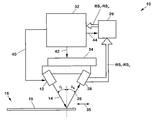
- FIG. 1 depicts a substrate surface identification system according to a preferred embodiment of the invention
- FIG. 2 depicts a radiation source and radiation sensor according to a preferred embodiment of the invention
- FIG. 3 depicts indicia formed on the surface of a substrate according to a preferred embodiment of the invention
- FIGS. 4A-4B depict scanning radiation over flat features and edge features of a recess in the surface of a substrate according to a preferred embodiment of the invention
- FIG. 5 depicts a flow chart of a method for scanning and identifying a substrate according to a preferred embodiment of the invention
- FIG. 6 depicts a functional block diagram of a system for identifying a substrate according to a preferred embodiment of the invention.
- FIG. 7 depicts a graphical representation of a character segment according to a preferred embodiment of the invention.
- a substrate identification system 10 for identifying a substrate 16 , such as an integrated circuit substrate as may be formed of a semiconductor material, such as silicon or gallium arsenide.
- the substrate 16 preferably undergoes an identification process at various points in an integrated circuit fabrication process flow. As the substrate 16 proceeds through the fabrication process, some physical characteristics of the surface of the substrate 16 tend to change, thus altering the visual characteristics of any identifying indicia on the surface 15 of the substrate 16 .
- the system 10 is operable to detect those aspects of the identifying indicia on the surface of the substrate 16 that do not tend to change as much as other aspects of the identifying indicia.
- the system 10 as described herein is implemented at several different fabrication stations, inspection stations, and test stations, and most preferably all such, to provide reliable identification of the substrate 16 at any particular point in the fabrication process.
- substrate identification means such as indicia 20 are formed in a surface 15 of the substrate 16 .
- the indicia 20 may be a combination of alphanumeric characters that is unique to a particular substrate 16 .
- the indicia 20 may have no relevance as far as standardized numbers or alphabet are concerned, but are formed to be relatively unique from one substrate 16 to another, so that the system 10 can distinguish one substrate 16 from another, and identify the given substrate 16 to other systems, as described in more detail below.
- the indicia 20 preferably comprise a pattern of recesses 21 in the surface 15 formed by the selective removal of substrate material, such as by laser ablation, or chemical or physical etching.
- the recesses 21 within the indicia 20 are preferably about four microns wide by about four microns deep, although the operation of the invention is not dependent upon any particular dimensional constraints of the recesses 21 .
- there are various characteristics of the identification system 10 that are preferably determined based at least in part upon the size of the recesses 21 , as described in more detail below.
- FIGS. 4A and 4B depict a cross-sectional view corresponding to the section line IV-IV′ shown in FIG. 3 .
- the characters in the indicia 20 such as the character “I” in the identification string “LSI0401”, include edge features 24 at the edges of the recesses 21 , and substantially flat features 22 between the recesses 21 .
- the edge features 24 are depicted in FIGS. 4A and 4B as substantially vertical, it is appreciated that the edge features in other embodiments are sloping, curved, or undercut depending on the method used to form the recesses 21 .
- the features 22 are depicted as substantially flat, they may actually have some degree of surface roughness or waviness, depending on the processing which has been performed on the substrate 16 .
- the system 10 includes a radiation source 12 for generating radiation such as a light beam 14 that is incident upon the surface 15 of the substrate 16 at an incidence angle ⁇ I with respect to normal to the surface 15 (step 102 ).
- the illumination source 12 includes a low-power light and associated optics for providing the incident illumination 14 in the form of a planar light beam 14 .
- the beam 14 provides a light footprint 18 having a footprint length L LF and a footprint width W LF on the surface 15 of the substrate 16 .
- the width W LF of the light footprint 18 is preferably no greater than about one-half to one quarter the breadth of a recess 21 .
- the radiation generated by the radiation source 12 is at a wavelength that is reflected by the material of the substrate 16 .
- the radiation is reflected by the substrate 16 , but not the other materials that may be deposited on the substrate 16 as it is processed.
- the substrate 16 is partially transparent to the radiation, but receptors on the other side of the substrate 16 from the radiation source 12 are operable to detect subtle variations in a characteristic of the transmitted radiation, such as either intensity, phase, or transmission angle.
- the invention as described herein is not specifically limited to those embodiments that are described with greater particularity below.
- the radiation footprint 18 may be much smaller than that as depicted in FIG. 3 .
- the radiation footprint 18 may be a dot having a diameter as determined by the size considerations as given elsewhere herein, which dot is scanned back and forth across the surface 15 of the substrate 16 in the area where the indicia 20 is formed.
- the illumination source 12 operates at a wavelength which does not adversely affect any of the substrate processing steps, or the materials used during such, or the structures thereby formed in the substrate 16 .
- the wavelength of radiation produced by the radiation source 12 is about 640 nanometers.
- the incident illumination 14 is depicted in FIGS. 4A and 4B as a series of parallel rays.
- the reflected illumination 26 is substantially specular, such that a substantial portion of the reflected illumination 26 propagates at a reflection angle ⁇ R which is substantially equivalent to the incidence angle ⁇ I .
- the intensity of the reflected illumination 26 at the angle ⁇ R is determined by the intensity of the incident illumination 14 and the reflectivity of the surface of the flat feature 22 .
- the intensity of the illumination 26 reflected from a flat feature 22 is referred to herein as a second intensity.
- the reflected illumination 26 is not specular, but rather is scattered at angles other than ⁇ R with respect to normal to the surface 15 . Due to the edge scattering, the intensity of the illumination 26 reflected from an edge feature 24 in the specular direction (at the angle ⁇ R ) is substantially less than the intensity of the illumination 26 reflected in the specular direction from a flat feature 22 .
- the intensity of the illumination 26 reflected from an edge feature 24 is referred to herein as a first intensity.
- the system 10 uses the difference in the intensity of the illumination reflected from an edge feature 24 as compared to the intensity of the illumination reflected from a flat feature 22 in forming an image of the indicia 20 .
- the system 10 in alternate embodiments has sensors disposed on an opposite side of the substrate 16 from the radiation source 12 , and uses the change in characteristics of the transmitted radiation from edge features 24 and flat features 22 .
- the system 10 includes a radiation sensor 28 for receiving the reflected illumination 26 propagating at the angle ⁇ R with respect to normal to the surface 15 .
- the radiation sensor 28 comprises an array of n number of optical detectors OD 1 -OD n .
- the radiation sensor 28 is a relatively small, single receptor.
- the radiation sensor 28 includes focusing optics for focusing the illumination 26 reflected from n number of incremental areas A 1 -A n of the surface 15 of the substrate 16 onto corresponding ones of the n number of detectors OD 1 -OD n .
- the width of each incremental area A 1 -A n is preferably no greater than about one-half to one quarter the breadth of a recess 21 .
- Each detector OD 1 -OD n preferably generates a corresponding analog electrical output signal RS 1 -RS n the amplitude of which is proportional to a characteristic of the radiation, such as the intensity of the illumination 26 reflected from the corresponding incremental area and propagating at the angle ⁇ R . Since the intensity of the reflected illumination 26 propagating at the angle ⁇ R is dependent on whether the incident illumination 14 impinges on a flat feature 22 or an edge feature 24 , the amplitude of each of the output signals RS 1 -RS n is also dependent at least in part on whether the illumination 26 is reflected from a flat feature 22 or an edge feature 24 within the illuminated incremental area A 1 -A n .
- the system 10 optionally includes a motion stage 34 for moving the source 12 and the sensor 28 in at least one scan direction 36 relative to the substrate 16 .
- the movement of the motion stage 34 is controlled by a processing system 32 , such as may be part of a personal computer, machine controller, or other dedicated computing device.
- the scanning of the substrate 16 is accomplished by external substrate staging means, such as a robotic arm that is a part of a substrate processing apparatus.
- the indicia 20 are scanned as the staging means inserts the substrate 16 into the system 10 , and no additional motion stage 34 is required.
- the surface 15 containing the indicia 20 is preferably moved relative to the light footprint 18 in a scan across the width W CS of the indicia 20 , so that the light footprint 18 sequentially illuminates substantially all of the features of the indicia 20 (step 104 ).
- movement such as in a transverse direction may also be desirable, based at least in part on the length of the radiation footprint 18 .
- flat features 22 and edge features 24 FIGGS.
- the array of radiation detectors: OD 1 -OD n receives reflected illumination 26 having the first intensity level from the edge features (step 106 ), and receives reflected illumination 26 having the second intensity level from the flat features (step 108 ).
- Each of the of detectors OD 1 -OD n detects a corresponding portion of the reflected illumination 26 and generates a corresponding output signal RS 1 -RS n which is provided to a signal conditioning circuit 29 (step 110 ).
- the signal conditioning circuit includes amplifiers, noise filters, and analog-to-digital converters which provide preprocessing conditioning of the output signals RS 1 -RS n . After filtering, amplification, and analog-to-digital conversion, the output signals RS 1 -RS n are provided to the processing system 32 .
- the processing system 32 processes the output signals RS 1 -RS n to form corresponding image portions of the indicia 20 (step 112 ).
- the processing of step 112 preferably includes converting each of the output signals RS 1 -RS n into a one-dimensional bit map of pixels having values corresponding to the amplitude of the corresponding output signal RS 1 -RS n as the light footprint 18 is scanned over the indicia 20 .
- the processing system 32 preferably combines the multiple one-dimensional bit maps to form a two-dimensional image of the indicia 20 (step 114 ).
- FIG. 6 Shown in FIG. 6 is a functional block diagram of exemplary functions executed by the processing system 32 in acquiring and processing the image of the indicia 20 .
- Each of the functions receives input from a knowledge base 50 .
- the knowledge base 50 is a collection of information related to characteristics of the substrate 16 , control parameters, character representation, etc.
- the information in the knowledge base 50 represents knowledge acquired by engineers and test operators over a period of time, during which substrates have been identified at various processing steps during the manufacturing of an integrated circuit.
- the various types of information provided in the knowledge base 50 are explained in more detail in the following discussion of the various functions of the processing system 32 .
- the image acquisition function 52 includes the generation of control signals which control the illumination source 12 and the motion stage 34 .
- the image acquisition function 52 generates an intensity control signal 40 (FIG. 1) for controlling the intensity of the illumination 14 provided by the illumination source 12 .
- the illumination intensity may be adjusted based upon the material which comprises the uppermost layer of the substrate 16 , the composition of which is generally dependent upon the point in the manufacturing process at which the substrate 16 is being identified.
- the speed at which the motion stage 34 scans the incident illumination 14 over the indicia 20 may be controlled by a motion control signal 42 (FIG. 1) generated by the image acquisition function 52 .
- These preferred intensity settings and speed settings are preferably stored in the knowledge base 50 .
- the preprocessing function 54 includes the generation of control signals which control the signal conditioning circuit 29 .
- the preprocessing function 54 preferably generates control signals 44 (FIG. 1) for controlling the amplitude of the output signals RS 1 -RS n and the shape of noise filter functions applied to the output signals RS 1 -RS n .
- control signals 44 FIG. 1
- These preferred amplifier and filter settings which may also be dependent on the point in the manufacturing process at which the substrate 16 is being identified, are preferably also stored in the knowledge base 50 .
- the segmentation and representation function 56 breaks the two-dimensional image of the indicia 20 into separate segments, and represents each segment as a two-dimensional image.
- each character segment such as the “L” segment 60
- each character segment preferably includes only one complete character.
- boundaries of the character segments are determined by position.
- the segment 60 is defined by the incremental areas A 1 to A 12 scanned over the indicia width W CS .
- segment boundaries may be determined by other means, such as by finding “blank space” between characters based on adjacent output signals having a constant intensity (indicating no recesses 21 ) over a complete scan of the indicia width W CS .
- FIG. 7 depicts a representation of the surface topology of the character “L” after noise filtering, analog-to-digital conversion, and segmentation.
- the peaks in the inverted output signal correspond to the recesses 21 (FIG. 3) which form the “L” in the surface 15 of the substrate 16 . Only peaks that are above a threshold level are used in the subsequent recognition function 58 . Peaks which fall below the threshold level are discarded as surface imperfections or noise.
- the threshold levels which may be different for different processing stages during fabrication and inspection of the substrate 16 , are preferably stored in the knowledge base 50 .
- the recognition function 58 compares the representation of a character, such as depicted in FIG. 7, to character patterns stored in the knowledge base 50 , and the character pattern which best matches the representation is selected (step 116 ).
- the recognition function 58 repeats this process for each character representation from each segment, and generates an identification string corresponding to the recognized indicia 20 , which in a preferred embodiment comprise alphanumeric characters.
- the processing system 32 Based on the alphanumeric textual string, the processing system 32 identifies the substrate 16 , such as by using a relational database stored in the processing system 32 or in another processing system connected to the system 32 by a network (step 118 ).
- the system 10 provides several benefits not realized by identification systems incorporating CCD cameras.
- the optical components of the system 10 including the source 12 and the receiver 28 , may be implemented in a compact package which may be installed at practically every fabrication process station.
- the system 10 since the system 10 may be implemented without expensive high-performance central processing units as are required to process the color and grayscale images produced by CCD cameras, the system 10 is less expensive.
- the system 10 does not require constant teaching and learning using a calibration substrate to recognize the indicia 20 . Rather, the system 10 need only be taught once the pattern of recesses which makes up each character.
- the operation of the system 10 is not substantially affected by changes in environmental lighting conditions, or changes in the color or reflectivity of the surface of the substrate from one process step to the next.
- relative movement between the substrate and the source/receiver is accomplished by moving the source/receiver and keeping the substrate stationary.
- the relative movement could also be accomplished by moving the substrate and keeping the source/detector stationary.
- the scope of the invention is not limited by the manner in which relative motion between the substrate and the source/receiver is accomplished.
- the source/receiver could be configured to scan across the length of the indicia rather than across the width.
- the scope of the invention is not limited by the scanning direction.
- scanning may also be accomplished by rotating the illumination source relative to the substrate, thereby sweeping the illumination beam over the indicia.
- the system is preferably configured to maintain ⁇ 1 equal to ⁇ R as the illumination beam is swept over the indicia.
Abstract
Description
Claims (14)
Priority Applications (1)
| Application Number | Priority Date | Filing Date | Title |
|---|---|---|---|
| US10/021,829 US6573523B1 (en) | 2001-12-12 | 2001-12-12 | Substrate surface scanning |
Applications Claiming Priority (1)
| Application Number | Priority Date | Filing Date | Title |
|---|---|---|---|
| US10/021,829 US6573523B1 (en) | 2001-12-12 | 2001-12-12 | Substrate surface scanning |
Publications (1)
| Publication Number | Publication Date |
|---|---|
| US6573523B1 true US6573523B1 (en) | 2003-06-03 |
Family
ID=21806383
Family Applications (1)
| Application Number | Title | Priority Date | Filing Date |
|---|---|---|---|
| US10/021,829 Expired - Lifetime US6573523B1 (en) | 2001-12-12 | 2001-12-12 | Substrate surface scanning |
Country Status (1)
| Country | Link |
|---|---|
| US (1) | US6573523B1 (en) |
Cited By (21)
| Publication number | Priority date | Publication date | Assignee | Title |
|---|---|---|---|---|
| US20030150917A1 (en) * | 1999-06-07 | 2003-08-14 | Tsikos Constantine J. | Planar light illumination and imaging (PLIIM) system employing led-based planar light illumination arrays (PLIAS) and an area-type image detection array |
| US20050190956A1 (en) * | 2004-02-26 | 2005-09-01 | Omron Corporation | Mounting-error inspecting method and substrate inspecting apparatus using the method |
| US20050230477A1 (en) * | 1999-06-07 | 2005-10-20 | Metrologic Instruments, Inc. | Planar laser illumination and imaging system |
| US20060002510A1 (en) * | 2004-06-30 | 2006-01-05 | Omron Corporation | Inspection method and system for and method of producing component mounting substrate |
| US20070108288A1 (en) * | 2005-11-16 | 2007-05-17 | Caskey Gregory T | Method and apparatus for novel reading of surface structure bar codes |
| US20080085565A1 (en) * | 2002-08-20 | 2008-04-10 | Cyvera Corporation | Method of reading encoded particles |
| US7898735B2 (en) | 2002-09-12 | 2011-03-01 | Illumina, Inc. | Methods and systems for writing an optical code within or on a fiber substrate |
| US7901630B2 (en) | 2002-08-20 | 2011-03-08 | Illumina, Inc. | Diffraction grating-based encoded microparticle assay stick |
| US7900836B2 (en) * | 2002-08-20 | 2011-03-08 | Illumina, Inc. | Optical reader system for substrates having an optically readable code |
| US8049893B2 (en) | 2003-01-22 | 2011-11-01 | Illumina, Inc. | Methods of identifying analytes and using encoded particles |
| US8081792B2 (en) | 2003-08-20 | 2011-12-20 | Illumina, Inc. | Fourier scattering methods for encoding microbeads and methods and apparatus for reading the same |
| US20120022680A1 (en) * | 2008-06-26 | 2012-01-26 | Sumitomo Metal Industries, Ltd. | Two-dimensional code reading device, two-dimensional code reading method, method of controlling manufacturing history information of member having substantially circular section orthogonal to the central axis thereof, and method of manufacturing the member using the control method |
| US8393419B1 (en) * | 2008-03-13 | 2013-03-12 | Us Synthetic Corporation | Superabrasive elements having indicia and related apparatus and methods |
| US8470605B2 (en) | 2002-09-12 | 2013-06-25 | Illumina, Inc. | Optical reader for reading encoded microparticles |
| US8498052B2 (en) | 2002-08-20 | 2013-07-30 | Illumina, Inc. | Composition including an item and an encoded optical substrate and a method for identifying an item |
| US8614852B2 (en) | 2002-08-20 | 2013-12-24 | Illumina, Inc. | Elongated microparticles having an optically detectable code configured to at least one of reflect or filter light |
| US20180018484A1 (en) * | 2016-07-14 | 2018-01-18 | Biotronik Se & Co. Kg | Identification of Miniaturized Electronic Assembly Using Identification Features on Multiple Components |
| CN107710231A (en) * | 2015-06-30 | 2018-02-16 | 日立汽车系统株式会社 | It is managed individual and imprint method |
| CN107710232A (en) * | 2015-06-30 | 2018-02-16 | 日立汽车系统株式会社 | Managed object and identification method |
| CN110346400A (en) * | 2019-06-18 | 2019-10-18 | 北京科技大学 | A kind of experimental rig and method for simulating Cannon burning |
| JP2020167286A (en) * | 2019-03-29 | 2020-10-08 | Juki株式会社 | Inspection apparatus and inspection method |
Citations (4)
| Publication number | Priority date | Publication date | Assignee | Title |
|---|---|---|---|---|
| US3714632A (en) * | 1971-03-30 | 1973-01-30 | Data Card Corp | Character recognition method and system with strobe control |
| US5247166A (en) * | 1991-05-31 | 1993-09-21 | Gtech Corporation | Form reader with linear CCD scanner and drum feed |
| US5481095A (en) * | 1992-02-17 | 1996-01-02 | Mitsubishi Denki Kabushiki Kaisha | Code reading pattern and an image pickup apparatus for reading the pattern |
| US5677522A (en) * | 1993-07-21 | 1997-10-14 | Sensis Corporation | Method and apparatus for non-contact reading of a relief pattern |
-
2001
- 2001-12-12 US US10/021,829 patent/US6573523B1/en not_active Expired - Lifetime
Patent Citations (4)
| Publication number | Priority date | Publication date | Assignee | Title |
|---|---|---|---|---|
| US3714632A (en) * | 1971-03-30 | 1973-01-30 | Data Card Corp | Character recognition method and system with strobe control |
| US5247166A (en) * | 1991-05-31 | 1993-09-21 | Gtech Corporation | Form reader with linear CCD scanner and drum feed |
| US5481095A (en) * | 1992-02-17 | 1996-01-02 | Mitsubishi Denki Kabushiki Kaisha | Code reading pattern and an image pickup apparatus for reading the pattern |
| US5677522A (en) * | 1993-07-21 | 1997-10-14 | Sensis Corporation | Method and apparatus for non-contact reading of a relief pattern |
Cited By (37)
| Publication number | Priority date | Publication date | Assignee | Title |
|---|---|---|---|---|
| US7104455B2 (en) * | 1999-06-07 | 2006-09-12 | Metrologic Instruments, Inc. | Planar light illumination and imaging (PLIIM) system employing LED-based planar light illumination arrays (PLIAS) and an area-type image detection array |
| US20030150917A1 (en) * | 1999-06-07 | 2003-08-14 | Tsikos Constantine J. | Planar light illumination and imaging (PLIIM) system employing led-based planar light illumination arrays (PLIAS) and an area-type image detection array |
| US20050230477A1 (en) * | 1999-06-07 | 2005-10-20 | Metrologic Instruments, Inc. | Planar laser illumination and imaging system |
| US20110033948A9 (en) * | 2002-08-20 | 2011-02-10 | Cyvera Corporation | Method of reading encoded particles |
| US8498052B2 (en) | 2002-08-20 | 2013-07-30 | Illumina, Inc. | Composition including an item and an encoded optical substrate and a method for identifying an item |
| US8333325B2 (en) | 2002-08-20 | 2012-12-18 | Illumina, Inc. | Optical reader system for substrates having an optically readable code |
| US20080085565A1 (en) * | 2002-08-20 | 2008-04-10 | Cyvera Corporation | Method of reading encoded particles |
| US8614852B2 (en) | 2002-08-20 | 2013-12-24 | Illumina, Inc. | Elongated microparticles having an optically detectable code configured to at least one of reflect or filter light |
| US7901630B2 (en) | 2002-08-20 | 2011-03-08 | Illumina, Inc. | Diffraction grating-based encoded microparticle assay stick |
| US7900836B2 (en) * | 2002-08-20 | 2011-03-08 | Illumina, Inc. | Optical reader system for substrates having an optically readable code |
| US7923260B2 (en) | 2002-08-20 | 2011-04-12 | Illumina, Inc. | Method of reading encoded particles |
| US8470605B2 (en) | 2002-09-12 | 2013-06-25 | Illumina, Inc. | Optical reader for reading encoded microparticles |
| US7898735B2 (en) | 2002-09-12 | 2011-03-01 | Illumina, Inc. | Methods and systems for writing an optical code within or on a fiber substrate |
| US9268983B2 (en) | 2003-01-22 | 2016-02-23 | Illumina, Inc. | Optical system and method for reading encoded microbeads |
| US8049893B2 (en) | 2003-01-22 | 2011-11-01 | Illumina, Inc. | Methods of identifying analytes and using encoded particles |
| US8081792B2 (en) | 2003-08-20 | 2011-12-20 | Illumina, Inc. | Fourier scattering methods for encoding microbeads and methods and apparatus for reading the same |
| US8565475B2 (en) | 2003-08-20 | 2013-10-22 | Illumina, Inc. | Optical system and method for reading encoded microbeads |
| US7356176B2 (en) * | 2004-02-26 | 2008-04-08 | Omron Corporation | Mounting-error inspecting method and substrate inspecting apparatus using the method |
| US20050190956A1 (en) * | 2004-02-26 | 2005-09-01 | Omron Corporation | Mounting-error inspecting method and substrate inspecting apparatus using the method |
| US7310406B2 (en) * | 2004-06-30 | 2007-12-18 | Omron Corporation | Inspection method and system for and method of producing component mounting substrate |
| US20060002510A1 (en) * | 2004-06-30 | 2006-01-05 | Omron Corporation | Inspection method and system for and method of producing component mounting substrate |
| US20070108288A1 (en) * | 2005-11-16 | 2007-05-17 | Caskey Gregory T | Method and apparatus for novel reading of surface structure bar codes |
| US8393419B1 (en) * | 2008-03-13 | 2013-03-12 | Us Synthetic Corporation | Superabrasive elements having indicia and related apparatus and methods |
| US8602130B1 (en) * | 2008-03-13 | 2013-12-10 | Us Synthetic Corporation | Superabrasive elements having indicia and related apparatus and methods |
| US8651382B2 (en) * | 2008-06-26 | 2014-02-18 | Nippon Steel & Sumitomo Metal Corporation | Two-dimensional code reading device, two-dimensional code reading method, method of controlling manufacturing history information of member having substantially circular section orthogonal to the central axis thereof, and method of manufacturing the member using the control method |
| US20120022680A1 (en) * | 2008-06-26 | 2012-01-26 | Sumitomo Metal Industries, Ltd. | Two-dimensional code reading device, two-dimensional code reading method, method of controlling manufacturing history information of member having substantially circular section orthogonal to the central axis thereof, and method of manufacturing the member using the control method |
| US10489697B2 (en) * | 2015-06-30 | 2019-11-26 | Hitachi Automotive Systems, Ltd. | Article and engraving method |
| CN107710231A (en) * | 2015-06-30 | 2018-02-16 | 日立汽车系统株式会社 | It is managed individual and imprint method |
| CN107710232A (en) * | 2015-06-30 | 2018-02-16 | 日立汽车系统株式会社 | Managed object and identification method |
| US20180174007A1 (en) * | 2015-06-30 | 2018-06-21 | Hitachi Automotive Systems, Ltd. | Managed article and engraving method |
| US20180197054A1 (en) * | 2015-06-30 | 2018-07-12 | Hitachi Automotive Systems, Ltd. | Managed article and code engraving method |
| CN107710232B (en) * | 2015-06-30 | 2021-05-04 | 日立汽车系统株式会社 | Managed object and identification method |
| US10489696B2 (en) * | 2015-06-30 | 2019-11-26 | Hitachi Automotive Systems, Ltd. | Article and code engraving method |
| US20180018484A1 (en) * | 2016-07-14 | 2018-01-18 | Biotronik Se & Co. Kg | Identification of Miniaturized Electronic Assembly Using Identification Features on Multiple Components |
| US10152621B2 (en) * | 2016-07-14 | 2018-12-11 | Biotronik Se & Co. Kg | Identification of miniaturized electronic assembly using identification features on multiple components |
| JP2020167286A (en) * | 2019-03-29 | 2020-10-08 | Juki株式会社 | Inspection apparatus and inspection method |
| CN110346400A (en) * | 2019-06-18 | 2019-10-18 | 北京科技大学 | A kind of experimental rig and method for simulating Cannon burning |
Similar Documents
| Publication | Publication Date | Title |
|---|---|---|
| US6573523B1 (en) | Substrate surface scanning | |
| US8639019B2 (en) | Method and apparatus for inspecting pattern defects | |
| US7949178B2 (en) | Pattern inspection method and its apparatus | |
| US9075026B2 (en) | Defect inspection device and defect inspection method | |
| JP5663207B2 (en) | Modular optical inspection system | |
| JP5028014B2 (en) | Pattern inspection method and apparatus | |
| US20080304734A1 (en) | Alignment correction prio to image sampling in inspection systems | |
| JP4472341B2 (en) | Defect detection method | |
| JP2008039533A (en) | Method for inspecting defect and apparatus therefor | |
| EP0406030B1 (en) | Inspection apparatus and method for detecting flaws on a diffractive surface | |
| US7106432B1 (en) | Surface inspection system and method for using photo detector array to detect defects in inspection surface | |
| KR101106722B1 (en) | Method for detecting defects | |
| JP3878340B2 (en) | Pattern defect inspection method and apparatus | |
| JPH0658215B2 (en) | Method and apparatus for inspecting a pattern to be inspected on a semiconductor wafer | |
| JPH06229936A (en) | Method and equipment for detecting pattern defect | |
| JP2001255279A (en) | Pattern defect inspection method and its device | |
| JP2002168799A (en) | Pattern defect inspection method | |
| JPH05129397A (en) | Foreign matter detection method and device | |
| JP3189604B2 (en) | Inspection method and device | |
| JP2006003168A (en) | Measurement method for surface shape and device therefor | |
| JP3198105B2 (en) | Automatic visual inspection device | |
| JPH04316346A (en) | Pattern recognition method | |
| JP3040013B2 (en) | Foreign object detection method using floating threshold | |
| JP3182517B2 (en) | Defect detection apparatus and method | |
| JPH08219740A (en) | Method and equipment for inspecting semiconductor device |
Legal Events
| Date | Code | Title | Description |
|---|---|---|---|
| AS | Assignment |
Owner name: LSI LOGIC CORPORATION, CALIFORNIA Free format text: ASSIGNMENT OF ASSIGNORS INTEREST;ASSIGNOR:LONG, THOMAS F.;REEL/FRAME:012402/0872 Effective date: 20011212 |
|
| STCF | Information on status: patent grant |
Free format text: PATENTED CASE |
|
| FPAY | Fee payment |
Year of fee payment: 4 |
|
| SULP | Surcharge for late payment | ||
| FEPP | Fee payment procedure |
Free format text: PAYOR NUMBER ASSIGNED (ORIGINAL EVENT CODE: ASPN); ENTITY STATUS OF PATENT OWNER: LARGE ENTITY |
|
| FPAY | Fee payment |
Year of fee payment: 8 |
|
| AS | Assignment |
Owner name: DEUTSCHE BANK AG NEW YORK BRANCH, AS COLLATERAL AG Free format text: PATENT SECURITY AGREEMENT;ASSIGNORS:LSI CORPORATION;AGERE SYSTEMS LLC;REEL/FRAME:032856/0031 Effective date: 20140506 |
|
| AS | Assignment |
Owner name: LSI CORPORATION, CALIFORNIA Free format text: CHANGE OF NAME;ASSIGNOR:LSI LOGIC CORPORATION;REEL/FRAME:033102/0270 Effective date: 20070406 |
|
| FPAY | Fee payment |
Year of fee payment: 12 |
|
| AS | Assignment |
Owner name: AVAGO TECHNOLOGIES GENERAL IP (SINGAPORE) PTE. LTD Free format text: ASSIGNMENT OF ASSIGNORS INTEREST;ASSIGNOR:LSI CORPORATION;REEL/FRAME:035390/0388 Effective date: 20140814 |
|
| AS | Assignment |
Owner name: AGERE SYSTEMS LLC, PENNSYLVANIA Free format text: TERMINATION AND RELEASE OF SECURITY INTEREST IN PATENT RIGHTS (RELEASES RF 032856-0031);ASSIGNOR:DEUTSCHE BANK AG NEW YORK BRANCH, AS COLLATERAL AGENT;REEL/FRAME:037684/0039 Effective date: 20160201 Owner name: LSI CORPORATION, CALIFORNIA Free format text: TERMINATION AND RELEASE OF SECURITY INTEREST IN PATENT RIGHTS (RELEASES RF 032856-0031);ASSIGNOR:DEUTSCHE BANK AG NEW YORK BRANCH, AS COLLATERAL AGENT;REEL/FRAME:037684/0039 Effective date: 20160201 |
|
| AS | Assignment |
Owner name: BANK OF AMERICA, N.A., AS COLLATERAL AGENT, NORTH CAROLINA Free format text: PATENT SECURITY AGREEMENT;ASSIGNOR:AVAGO TECHNOLOGIES GENERAL IP (SINGAPORE) PTE. LTD.;REEL/FRAME:037808/0001 Effective date: 20160201 Owner name: BANK OF AMERICA, N.A., AS COLLATERAL AGENT, NORTH Free format text: PATENT SECURITY AGREEMENT;ASSIGNOR:AVAGO TECHNOLOGIES GENERAL IP (SINGAPORE) PTE. LTD.;REEL/FRAME:037808/0001 Effective date: 20160201 |
|
| AS | Assignment |
Owner name: AVAGO TECHNOLOGIES GENERAL IP (SINGAPORE) PTE. LTD., SINGAPORE Free format text: TERMINATION AND RELEASE OF SECURITY INTEREST IN PATENTS;ASSIGNOR:BANK OF AMERICA, N.A., AS COLLATERAL AGENT;REEL/FRAME:041710/0001 Effective date: 20170119 Owner name: AVAGO TECHNOLOGIES GENERAL IP (SINGAPORE) PTE. LTD Free format text: TERMINATION AND RELEASE OF SECURITY INTEREST IN PATENTS;ASSIGNOR:BANK OF AMERICA, N.A., AS COLLATERAL AGENT;REEL/FRAME:041710/0001 Effective date: 20170119 |
|
| AS | Assignment |
Owner name: BELL SEMICONDUCTOR, LLC, ILLINOIS Free format text: ASSIGNMENT OF ASSIGNORS INTEREST;ASSIGNORS:AVAGO TECHNOLOGIES GENERAL IP (SINGAPORE) PTE. LTD.;BROADCOM CORPORATION;REEL/FRAME:044886/0766 Effective date: 20171208 |
|
| AS | Assignment |
Owner name: CORTLAND CAPITAL MARKET SERVICES LLC, AS COLLATERA Free format text: SECURITY INTEREST;ASSIGNORS:HILCO PATENT ACQUISITION 56, LLC;BELL SEMICONDUCTOR, LLC;BELL NORTHERN RESEARCH, LLC;REEL/FRAME:045216/0020 Effective date: 20180124 |
|
| AS | Assignment |
Owner name: BELL NORTHERN RESEARCH, LLC, ILLINOIS Free format text: RELEASE BY SECURED PARTY;ASSIGNOR:CORTLAND CAPITAL MARKET SERVICES LLC;REEL/FRAME:059723/0382 Effective date: 20220401 Owner name: BELL SEMICONDUCTOR, LLC, ILLINOIS Free format text: RELEASE BY SECURED PARTY;ASSIGNOR:CORTLAND CAPITAL MARKET SERVICES LLC;REEL/FRAME:059723/0382 Effective date: 20220401 Owner name: HILCO PATENT ACQUISITION 56, LLC, ILLINOIS Free format text: RELEASE BY SECURED PARTY;ASSIGNOR:CORTLAND CAPITAL MARKET SERVICES LLC;REEL/FRAME:059723/0382 Effective date: 20220401 |