US6542382B2 - Densely arranged electrically shielded communication panels - Google Patents
Densely arranged electrically shielded communication panels Download PDFInfo
- Publication number
- US6542382B2 US6542382B2 US09/947,154 US94715401A US6542382B2 US 6542382 B2 US6542382 B2 US 6542382B2 US 94715401 A US94715401 A US 94715401A US 6542382 B2 US6542382 B2 US 6542382B2
- Authority
- US
- United States
- Prior art keywords
- panels
- rack
- coupled
- conductive sheet
- printed circuit
- Prior art date
- Legal status (The legal status is an assumption and is not a legal conclusion. Google has not performed a legal analysis and makes no representation as to the accuracy of the status listed.)
- Expired - Fee Related
Links
- 239000000758 substrate Substances 0.000 claims description 13
- 238000000034 method Methods 0.000 claims description 5
- 230000009977 dual effect Effects 0.000 description 5
- 238000001816 cooling Methods 0.000 description 2
- 239000004020 conductor Substances 0.000 description 1
- 230000003287 optical effect Effects 0.000 description 1
- 238000005476 soldering Methods 0.000 description 1
Images


Classifications
-
- H—ELECTRICITY
- H05—ELECTRIC TECHNIQUES NOT OTHERWISE PROVIDED FOR
- H05K—PRINTED CIRCUITS; CASINGS OR CONSTRUCTIONAL DETAILS OF ELECTRIC APPARATUS; MANUFACTURE OF ASSEMBLAGES OF ELECTRICAL COMPONENTS
- H05K9/00—Screening of apparatus or components against electric or magnetic fields
- H05K9/0062—Structures of standardised dimensions, e.g. 19" rack, chassis for servers or telecommunications
-
- H—ELECTRICITY
- H04—ELECTRIC COMMUNICATION TECHNIQUE
- H04Q—SELECTING
- H04Q1/00—Details of selecting apparatus or arrangements
- H04Q1/02—Constructional details
- H04Q1/14—Distribution frames
-
- H—ELECTRICITY
- H04—ELECTRIC COMMUNICATION TECHNIQUE
- H04Q—SELECTING
- H04Q2201/00—Constructional details of selecting arrangements
- H04Q2201/10—Housing details
-
- H—ELECTRICITY
- H04—ELECTRIC COMMUNICATION TECHNIQUE
- H04Q—SELECTING
- H04Q2201/00—Constructional details of selecting arrangements
- H04Q2201/12—Printed circuits
Definitions
- This invention relates to communication distribution equipment, and more specifically to methods and apparatus for supporting a multiplicity of densely arranged or packed electrical shielded communication panels, each of which has a ground or conductive sheet covering the back side of the panel to provide back side shielding to the circuitry on that same panel as well as front side shielding to an adjacent panel.
- An apparatus for supporting a plurality of densely arranged electrically shielded communication panels includes a rack that supports at least two panels.
- the panels are supported adjacent to each other by the rack, and each panel includes at least two sides with a printed circuit on one side and a conductive sheet on the other side.
- the conductive sheet on each of the panels is coupled to an electrical connection point on the rack when the panel is placed in the rack.
- the two panels are placed in the rack such that the printed circuit of one of the panels is electrically shielded by the conductive sheet on another, closely aligned another one of the panels.
- FIG. 1 is a diagrammatic representation of a support structure or cabinet having at least one panel area, or rack with dimensions suitable for supporting densely-aligned panels of the present invention.
- Other panel areas or racks of the support structure or cabinet may include power supplies, light-emitting generators, cooling fans, and the like;
- FIG. 2 shows the panel area of FIG. 1, which receives the densely-aligned shielded panels of the present invention
- FIGS. 3 a, 3 b, and 3 c are a side view, front view, and bottom view respectively of one embodiment of electrically-shielded panels of the present invention suitable for being densely arranged with similar type panels;
- FIG. 4 is a highly enlarged and detailed view of the FIG. 3 c bottom view for illustrating details of the panel
- FIGS. 5 a and 5 b show still another embodiment of the shielded panels of the present invention.
- FIGS. 6 a, 6 b and 6 c show yet another embodiment of a panel of the present invention suitable for being densley arranged with like panels;
- FIG. 7 is another bottom view of the different type connector terminals used on the electrically-shielded panels of the present invention.
- a support structure or cabinet 10 which, in the embodiment shown, has at least one panel area or rack area 12 as well as second and third panel or rack areas 16 and 18 . It should be appreciated that the distribution within the structure or cabinet 10 may well include other areas for different panels, including other areas for panels of the present invention, such as panel or rack area 12 . However, for explanation purposes only, there is shown one panel or rack area 12 , a panel or rack area 16 with a power supply 20 and four optical transmitters 22 - 28 for generating light at specific wavelengths of light commonly referred to as ⁇ .
- the panel or rack area 18 typically might include a cooling fan 30 as well as four other additional optical-transmitting devices 32 - 38 for generating wavelengths of light still different from those of panels 22 , 24 , 26 , and 28 above.
- Cabinet 10 includes an electrical connection point 11 which typically is connected to ground.
- the panel or rack area 12 will include a rack or support pocket 40 , which will typically be a box-like structure supported in the cabinet 10 by support brackets 42 and 44 .
- the receiving rack 40 will include at least a bottom support member 46 and a top support member 48 .
- Each front portion or face plate includes a mounting screw or lug 92 received by support bracket 48 .
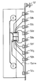
- panels 50 through 80 have eight input terminals in one group and a single output terminal at the bottom of the rack.
- the eight top terminals 50 a through 50 h are for receiving up to eight different input signals which may have the same or different frequencies, which signals are then combined and provided as a single output on the bottom output terminal 50 .
- Panels 82 through 88 are dual combining circuits. That is, there are two combining circuits on each panel.
- the panels illustrated in FIG. 2 show four different types of dual panels.
- panel 82 includes 10 connectors of the same type.
- the first four top connectors are input terminals, as discussed above.
- the next terminal, however, indicated in the drawing as 82 w, is a first output terminal providing a combined output to the signals received from the four top connectors.
- the next four terminals are the input terminals for the second combining circuit on panel 82
- terminal 82 x is the output terminal for the combined signals received from the bottom four input terminals.
- Panel 84 is almost identical to panel 82 , except the lower-most output terminal 84 z is larger than terminal 82 x and is for connecting to a larger connection terminal on heavy-duty coaxial cables.
- Panel 86 is similar to panel 84 , except the output terminal 86 y is also a large output terminal of the same type as 84 z. This larger connection terminal is often referred to as an “F” connector.
- the panel 88 does not include the top four input terminals or the top output terminals, as did panels 82 , 84 , and 86 .
- the circuits may be on the printed circuit board and just not brought to the front of the panel or in other instances, the circuit boards may be manufactured without these second circuits.
- FIGS. 3 a, 3 b, and 3 c there is shown a side view, a front view and a bottom view of the panel 50 , which, of course, is also similar to the panels 52 through 80 . These views clearly show the connecting lug 92 which is attached to the face plate or front portion 94 of panel 50 .
- a printed circuit board 96 extends perpendicularly to the face plate or front portion 94 of panel 50 .
- the face plate or front portion 94 of the panel itself includes a first edge member 98 for support and a second support member 100 , which it will be noticed also includes an extension 102 which abuts the conductive sheet 112 on the backside 104 of the printed circuit board 96 .
- the circuit board is used for combining electrical RF signals, each having a bandwidth around a different center frequency.
- the printed circuit board will include one connection path from each of the input terminals 50 a through 50 h such that each of these terminals provides a constant input impedance, such as, for example, 75 ohms.
- a single printed connection path will run from the common connection point of the output terminal 50 v, and would also provide a constant impedance from the connection point to the output terminal.
- the printed circuit board 96 will include an insulating substrate 106 , having a front side with a printed circuit thereon. In the portion of the circuit board shown in FIG. 4, part of the printed circuit is shown as section 108 .
- the printed circuit board will also include on the back side 10 of the substrate 106 a conductive sheet 112 , which is substantially co-extensive with the overall size of the printed circuit board.
- the conductive sheet 112 will typically act as a grounding plane to provide electrical shielding.
- the extension 102 of portion 94 of panel 50 is in electrical contact with the conductive sheet 112 .
- connection terminals 50 a through 50 h and 50 v include a rear portion 114 ; a throat portion 116 and an outward securing portion 118 , which may be unitary with the cable-receiving portion 120 .
- This type terminal is shown such that the throat portion 116 extends through an aperture 122 in front panel 94 to which is then attached the outward portion 118 .
- the diameter of portions 114 and 118 are larger than the aperture at 122 such that the terminal may be secured tightly to the faceplate 94 . This may be accomplished by tightening the outward portion 118 on threads cut into the portion 116 .
- This type of terminal may be referred to as an edge terminal, as it makes an electrical connection to the edges of conductive plate 112 and circuit portion 108 without requiring soldering or other permanent attachments.
- the printed circuit portion 108 and the conductive sheet 112 are in a tight frictional electrical contact with conductors 116 and 118 respectively on the internal portion of the terminal 114 .
- this panel includes a first portion or combination circuit which has input terminals 82 a through 82 d, which provide their inputs to a single output terminal 82 w and a second circuit, which includes inputs 82 e through 82 h, which have their inputs combined and provided on a single output 82 x.
- FIGS. 6 a and 6 b there is shown a panel design similar to that of panel 86 .
- panel 86 is substantially similar as the panel shown in FIG. 5 a, except it includes two heavy-duty connectors 86 y and 86 z.
- panel 84 it will substantially similar to the dual circuitry with respect to FIG. 5 a except it will include one small connector, such as connector 82 x and one large output connector such as 86 z.
- FIG. 6 c shows a front portion suitable for use with the dual circuit of FIG. 6 a where the first portion of the circuit, having inputs 88 a through 88 d and output 82 x are not brought out to the front panel.
- the circuitry portion used by the input terminals 88 a through 88 d and output terminal 86 y may either be provided and not brought to the front of the panel, or simply not printed onto the circuit board.
- FIG. 7 shows the bottom view of the panel such as shown in FIGS. 6 a, 6 b, and 6 c.
Abstract
Description
Claims (20)
Priority Applications (1)
| Application Number | Priority Date | Filing Date | Title |
|---|---|---|---|
| US09/947,154 US6542382B2 (en) | 1999-05-24 | 2001-09-05 | Densely arranged electrically shielded communication panels |
Applications Claiming Priority (3)
| Application Number | Priority Date | Filing Date | Title |
|---|---|---|---|
| US13562399P | 1999-05-24 | 1999-05-24 | |
| US09/410,975 US6310784B1 (en) | 1999-05-24 | 1999-10-04 | Densely arranged electrically shielded communication panels |
| US09/947,154 US6542382B2 (en) | 1999-05-24 | 2001-09-05 | Densely arranged electrically shielded communication panels |
Related Parent Applications (1)
| Application Number | Title | Priority Date | Filing Date |
|---|---|---|---|
| US09/410,975 Continuation US6310784B1 (en) | 1999-05-24 | 1999-10-04 | Densely arranged electrically shielded communication panels |
Publications (2)
| Publication Number | Publication Date |
|---|---|
| US20020030980A1 US20020030980A1 (en) | 2002-03-14 |
| US6542382B2 true US6542382B2 (en) | 2003-04-01 |
Family
ID=26833506
Family Applications (2)
| Application Number | Title | Priority Date | Filing Date |
|---|---|---|---|
| US09/410,975 Expired - Lifetime US6310784B1 (en) | 1999-05-24 | 1999-10-04 | Densely arranged electrically shielded communication panels |
| US09/947,154 Expired - Fee Related US6542382B2 (en) | 1999-05-24 | 2001-09-05 | Densely arranged electrically shielded communication panels |
Family Applications Before (1)
| Application Number | Title | Priority Date | Filing Date |
|---|---|---|---|
| US09/410,975 Expired - Lifetime US6310784B1 (en) | 1999-05-24 | 1999-10-04 | Densely arranged electrically shielded communication panels |
Country Status (3)
| Country | Link |
|---|---|
| US (2) | US6310784B1 (en) |
| EP (1) | EP1183877A1 (en) |
| WO (1) | WO2000072607A1 (en) |
Cited By (3)
| Publication number | Priority date | Publication date | Assignee | Title |
|---|---|---|---|---|
| US20070285910A1 (en) * | 2006-06-07 | 2007-12-13 | Hanoch Eshel | Communication Cabinet and a Method for Installing Active Components in a Communication Cabinet |
| US7379304B2 (en) * | 2001-02-06 | 2008-05-27 | Harris Corporation | Hub IDU card insert panel and method |
| US20100210142A1 (en) * | 2009-02-18 | 2010-08-19 | Cinch Connectors, Inc. | Electrical Connector |
Citations (17)
| Publication number | Priority date | Publication date | Assignee | Title |
|---|---|---|---|---|
| US4493010A (en) * | 1982-11-05 | 1985-01-08 | Lockheed Corporation | Electronic packaging module utilizing phase-change conductive cooling |
| DE8803544U1 (en) | 1988-03-16 | 1988-07-07 | Standard Elektrik Lorenz Ag, 7000 Stuttgart, De | |
| US4820200A (en) * | 1987-02-13 | 1989-04-11 | Switchcraft, Inc. | Slab-like jack module |
| EP0412045A2 (en) | 1989-08-04 | 1991-02-06 | Adc Telecommunications, Inc. | Digital cross-connect assembly |
| US5070430A (en) * | 1989-09-25 | 1991-12-03 | Siemens Aktiengesellschaft | Electrical installation composed of individual subassemblies |
| US5130986A (en) | 1990-04-27 | 1992-07-14 | At&T Bell Laboratories | High speed transport protocol with two windows |
| US5430615A (en) * | 1990-08-14 | 1995-07-04 | The Grass Valley Group, Inc. | Printed circuit board assembly |
| US5520554A (en) | 1994-04-07 | 1996-05-28 | Telefonaktiebolaget Lm Ericsson | Cable connection and shielding device |
| US5546292A (en) | 1994-08-12 | 1996-08-13 | Sylvan R. Shemitz Designs, Inc. | Hospital corridor lighting/information unit and system |
| US5641294A (en) * | 1995-05-31 | 1997-06-24 | Northern Telecom Limited | Backplane assembly including coaxial connectors |
| US5652697A (en) * | 1995-11-13 | 1997-07-29 | Ast Research, Inc. | Computer system backplane having ground tabs for interconnecting the backplane ground to the computer system chassis |
| US5913701A (en) * | 1997-02-28 | 1999-06-22 | Adc Telecommunications, Inc. | DSX module with removable switching jack |
| US6080930A (en) * | 1998-05-27 | 2000-06-27 | Nortel Networks Limited | ESD/EMC gasket |
| US6166919A (en) * | 1997-12-16 | 2000-12-26 | Notrel Networks Corporation | Casing mountable filler module |
| US6241562B1 (en) * | 1999-06-22 | 2001-06-05 | Avaya Technology Corp. | Digital cross connect/interconnect module |
| US6243273B1 (en) * | 1999-09-01 | 2001-06-05 | Nortel Networks Limited | Mini-backplane “T” assembly |
| US6327155B1 (en) * | 1999-12-16 | 2001-12-04 | Nortel Networks Limited | Method and apparatus for preventing flamespread in an equipment assembly |
Family Cites Families (9)
| Publication number | Priority date | Publication date | Assignee | Title |
|---|---|---|---|---|
| US5001602A (en) * | 1988-11-28 | 1991-03-19 | Reliance Comm/Tec Corporation | Network interface cabinet for large pair count telephone terminations |
| FR2652229B1 (en) * | 1989-09-19 | 1991-11-15 | Bull Sa | SHIELDING ASSEMBLY FOR A COLLECTOR BLOCK CONNECTED TO ELECTRICAL EQUIPMENT PLACED INSIDE A CHASSIS. |
| US5173845A (en) * | 1989-12-26 | 1992-12-22 | Star Technologies, Inc. | High density frontplane interconnection system |
| US5159534A (en) * | 1991-01-22 | 1992-10-27 | Johnson Service Company | Electronic/electromechanical packaging arrangement for facility management system |
| US5130896A (en) * | 1991-02-22 | 1992-07-14 | Hewlett-Packard Company | Apparatus for electromagnetic interference containment for printed circuit board connectors |
| US5078624A (en) * | 1991-05-28 | 1992-01-07 | Adc Telecommunications, Inc. | Digital signal cross-connect module |
| US5388995A (en) * | 1993-06-11 | 1995-02-14 | The Whitaker Corporation | EMI/RFI protective cable interface for high density junction box |
| US5546282A (en) * | 1995-05-02 | 1996-08-13 | Telect, Inc. | Telecommunication network digital cross-connect panels having insertable modules with printed circuit board mounted coaxial jack switches |
| US5980312A (en) * | 1998-01-12 | 1999-11-09 | Amphenol Corporation | Modular optical/electronic backplane assembly |
-
1999
- 1999-10-04 US US09/410,975 patent/US6310784B1/en not_active Expired - Lifetime
-
2000
- 2000-05-18 EP EP00930824A patent/EP1183877A1/en not_active Withdrawn
- 2000-05-18 WO PCT/US2000/013818 patent/WO2000072607A1/en not_active Application Discontinuation
-
2001
- 2001-09-05 US US09/947,154 patent/US6542382B2/en not_active Expired - Fee Related
Patent Citations (17)
| Publication number | Priority date | Publication date | Assignee | Title |
|---|---|---|---|---|
| US4493010A (en) * | 1982-11-05 | 1985-01-08 | Lockheed Corporation | Electronic packaging module utilizing phase-change conductive cooling |
| US4820200A (en) * | 1987-02-13 | 1989-04-11 | Switchcraft, Inc. | Slab-like jack module |
| DE8803544U1 (en) | 1988-03-16 | 1988-07-07 | Standard Elektrik Lorenz Ag, 7000 Stuttgart, De | |
| EP0412045A2 (en) | 1989-08-04 | 1991-02-06 | Adc Telecommunications, Inc. | Digital cross-connect assembly |
| US5070430A (en) * | 1989-09-25 | 1991-12-03 | Siemens Aktiengesellschaft | Electrical installation composed of individual subassemblies |
| US5130986A (en) | 1990-04-27 | 1992-07-14 | At&T Bell Laboratories | High speed transport protocol with two windows |
| US5430615A (en) * | 1990-08-14 | 1995-07-04 | The Grass Valley Group, Inc. | Printed circuit board assembly |
| US5520554A (en) | 1994-04-07 | 1996-05-28 | Telefonaktiebolaget Lm Ericsson | Cable connection and shielding device |
| US5546292A (en) | 1994-08-12 | 1996-08-13 | Sylvan R. Shemitz Designs, Inc. | Hospital corridor lighting/information unit and system |
| US5641294A (en) * | 1995-05-31 | 1997-06-24 | Northern Telecom Limited | Backplane assembly including coaxial connectors |
| US5652697A (en) * | 1995-11-13 | 1997-07-29 | Ast Research, Inc. | Computer system backplane having ground tabs for interconnecting the backplane ground to the computer system chassis |
| US5913701A (en) * | 1997-02-28 | 1999-06-22 | Adc Telecommunications, Inc. | DSX module with removable switching jack |
| US6166919A (en) * | 1997-12-16 | 2000-12-26 | Notrel Networks Corporation | Casing mountable filler module |
| US6080930A (en) * | 1998-05-27 | 2000-06-27 | Nortel Networks Limited | ESD/EMC gasket |
| US6241562B1 (en) * | 1999-06-22 | 2001-06-05 | Avaya Technology Corp. | Digital cross connect/interconnect module |
| US6243273B1 (en) * | 1999-09-01 | 2001-06-05 | Nortel Networks Limited | Mini-backplane “T” assembly |
| US6327155B1 (en) * | 1999-12-16 | 2001-12-04 | Nortel Networks Limited | Method and apparatus for preventing flamespread in an equipment assembly |
Cited By (9)
| Publication number | Priority date | Publication date | Assignee | Title |
|---|---|---|---|---|
| US7379304B2 (en) * | 2001-02-06 | 2008-05-27 | Harris Corporation | Hub IDU card insert panel and method |
| US20070285910A1 (en) * | 2006-06-07 | 2007-12-13 | Hanoch Eshel | Communication Cabinet and a Method for Installing Active Components in a Communication Cabinet |
| US7885082B2 (en) * | 2006-06-07 | 2011-02-08 | Teledata Networks Limited | Communication cabinet and a method for installing active components in a communication cabinet |
| US20100210142A1 (en) * | 2009-02-18 | 2010-08-19 | Cinch Connectors, Inc. | Electrical Connector |
| US20110195593A1 (en) * | 2009-02-18 | 2011-08-11 | Cinch Connectors, Inc. | Electrical Connector |
| US20110195592A1 (en) * | 2009-02-18 | 2011-08-11 | Cinch Connectors, Inc. | Electrical Connector |
| US8011950B2 (en) | 2009-02-18 | 2011-09-06 | Cinch Connectors, Inc. | Electrical connector |
| US8298009B2 (en) | 2009-02-18 | 2012-10-30 | Cinch Connectors, Inc. | Cable assembly with printed circuit board having a ground layer |
| US8337243B2 (en) | 2009-02-18 | 2012-12-25 | Cinch Connectors, Inc. | Cable assembly with a material at an edge of a substrate |
Also Published As
| Publication number | Publication date |
|---|---|
| EP1183877A1 (en) | 2002-03-06 |
| US20020030980A1 (en) | 2002-03-14 |
| WO2000072607A8 (en) | 2001-03-29 |
| WO2000072607A1 (en) | 2000-11-30 |
| US6310784B1 (en) | 2001-10-30 |
Similar Documents
| Publication | Publication Date | Title |
|---|---|---|
| USRE43820E1 (en) | RF circuit module and chassis including amplifier | |
| US6414636B1 (en) | Radio frequency connector for reducing passive inter-modulation effects | |
| US4954929A (en) | Multi-layer circuit board that suppresses radio frequency interference from high frequency signals | |
| US7086869B1 (en) | Flexible cable interconnect with integrated EMC shielding | |
| AU1741400A (en) | Electrical connector | |
| US5668509A (en) | Modified coaxial to GCPW vertical solderless interconnects for stack MIC assemblies | |
| US4970625A (en) | Integrated module handle and chassis bulkhead for reducing electromagnetic interference emissions from circuit modules | |
| US6683254B1 (en) | Low loss cable coupler | |
| US20140232469A1 (en) | Rf power amplifier and method of assembly for same | |
| US5561584A (en) | Electrical ground plane apparatus | |
| US20060267713A1 (en) | Low cost highly isolated RF coupler | |
| US6541711B1 (en) | Isolated ground circuit board apparatus | |
| US6473043B1 (en) | Antenna assembly | |
| JP4582961B2 (en) | Tuner with no RF input pin / lead on edge | |
| US20030168235A1 (en) | EMI shielded module | |
| US6542382B2 (en) | Densely arranged electrically shielded communication panels | |
| US6635821B2 (en) | Module having angled receptacle | |
| US6624503B1 (en) | Electromagnetic filtering structure | |
| US5788511A (en) | Universal connector pad | |
| US6137061A (en) | Reduction of parasitic through hole via capacitance in multilayer printed circuit boards | |
| KR100868928B1 (en) | Method and apparatus for reducing electromagnetic radiation | |
| US5620341A (en) | ESD and EMI protected ethernet LAN tap | |
| JP3718119B2 (en) | Television signal transmitter | |
| JP2001255970A (en) | Electronic equipment | |
| JP3747753B2 (en) | Switching distributor |
Legal Events
| Date | Code | Title | Description |
|---|---|---|---|
| AS | Assignment |
Owner name: MARCONI INTELLECTUAL PROPERTY (RINGFENCE)INC., PEN Free format text: ASSIGNMENT OF ASSIGNORS INTEREST;ASSIGNOR:MARCONI COMMUNICATIONS, INC.;REEL/FRAME:014646/0607 Effective date: 20031028 |
|
| AS | Assignment |
Owner name: ADVANCED FIBRE ACCESS CORPORATION, CALIFORNIA Free format text: ASSIGNMENT OF ASSIGNORS INTEREST;ASSIGNOR:MARCONI INTELLECTUAL PROPERTY (RINGFENCE), INC.;REEL/FRAME:014532/0723 Effective date: 20040220 |
|
| AS | Assignment |
Owner name: TELLABS BEDFORD, INC., TEXAS Free format text: CHANGE OF NAME;ASSIGNOR:ADVANCED FIBRE ACCESS CORPORATION;REEL/FRAME:016269/0577 Effective date: 20041208 |
|
| FPAY | Fee payment |
Year of fee payment: 4 |
|
| FEPP | Fee payment procedure |
Free format text: PAYOR NUMBER ASSIGNED (ORIGINAL EVENT CODE: ASPN); ENTITY STATUS OF PATENT OWNER: LARGE ENTITY |
|
| FEPP | Fee payment procedure |
Free format text: PAYER NUMBER DE-ASSIGNED (ORIGINAL EVENT CODE: RMPN); ENTITY STATUS OF PATENT OWNER: LARGE ENTITY Free format text: PAYOR NUMBER ASSIGNED (ORIGINAL EVENT CODE: ASPN); ENTITY STATUS OF PATENT OWNER: LARGE ENTITY |
|
| FPAY | Fee payment |
Year of fee payment: 8 |
|
| FEPP | Fee payment procedure |
Free format text: PAYER NUMBER DE-ASSIGNED (ORIGINAL EVENT CODE: RMPN); ENTITY STATUS OF PATENT OWNER: LARGE ENTITY Free format text: PAYOR NUMBER ASSIGNED (ORIGINAL EVENT CODE: ASPN); ENTITY STATUS OF PATENT OWNER: LARGE ENTITY |
|
| REMI | Maintenance fee reminder mailed | ||
| LAPS | Lapse for failure to pay maintenance fees | ||
| STCH | Information on status: patent discontinuation |
Free format text: PATENT EXPIRED DUE TO NONPAYMENT OF MAINTENANCE FEES UNDER 37 CFR 1.362 |
|
| FP | Lapsed due to failure to pay maintenance fee |
Effective date: 20150401 |