US6534007B1 - Method and apparatus for detecting the endpoint of a chamber cleaning - Google Patents
Method and apparatus for detecting the endpoint of a chamber cleaning Download PDFInfo
- Publication number
- US6534007B1 US6534007B1 US08/904,432 US90443297A US6534007B1 US 6534007 B1 US6534007 B1 US 6534007B1 US 90443297 A US90443297 A US 90443297A US 6534007 B1 US6534007 B1 US 6534007B1
- Authority
- US
- United States
- Prior art keywords
- chamber
- plasma
- interior
- vacuum chamber
- photodetector
- Prior art date
- Legal status (The legal status is an assumption and is not a legal conclusion. Google has not performed a legal analysis and makes no representation as to the accuracy of the status listed.)
- Expired - Fee Related
Links
Images


Classifications
-
- C—CHEMISTRY; METALLURGY
- C23—COATING METALLIC MATERIAL; COATING MATERIAL WITH METALLIC MATERIAL; CHEMICAL SURFACE TREATMENT; DIFFUSION TREATMENT OF METALLIC MATERIAL; COATING BY VACUUM EVAPORATION, BY SPUTTERING, BY ION IMPLANTATION OR BY CHEMICAL VAPOUR DEPOSITION, IN GENERAL; INHIBITING CORROSION OF METALLIC MATERIAL OR INCRUSTATION IN GENERAL
- C23C—COATING METALLIC MATERIAL; COATING MATERIAL WITH METALLIC MATERIAL; SURFACE TREATMENT OF METALLIC MATERIAL BY DIFFUSION INTO THE SURFACE, BY CHEMICAL CONVERSION OR SUBSTITUTION; COATING BY VACUUM EVAPORATION, BY SPUTTERING, BY ION IMPLANTATION OR BY CHEMICAL VAPOUR DEPOSITION, IN GENERAL
- C23C14/00—Coating by vacuum evaporation, by sputtering or by ion implantation of the coating forming material
- C23C14/22—Coating by vacuum evaporation, by sputtering or by ion implantation of the coating forming material characterised by the process of coating
- C23C14/56—Apparatus specially adapted for continuous coating; Arrangements for maintaining the vacuum, e.g. vacuum locks
- C23C14/564—Means for minimising impurities in the coating chamber such as dust, moisture, residual gases
-
- C—CHEMISTRY; METALLURGY
- C23—COATING METALLIC MATERIAL; COATING MATERIAL WITH METALLIC MATERIAL; CHEMICAL SURFACE TREATMENT; DIFFUSION TREATMENT OF METALLIC MATERIAL; COATING BY VACUUM EVAPORATION, BY SPUTTERING, BY ION IMPLANTATION OR BY CHEMICAL VAPOUR DEPOSITION, IN GENERAL; INHIBITING CORROSION OF METALLIC MATERIAL OR INCRUSTATION IN GENERAL
- C23C—COATING METALLIC MATERIAL; COATING MATERIAL WITH METALLIC MATERIAL; SURFACE TREATMENT OF METALLIC MATERIAL BY DIFFUSION INTO THE SURFACE, BY CHEMICAL CONVERSION OR SUBSTITUTION; COATING BY VACUUM EVAPORATION, BY SPUTTERING, BY ION IMPLANTATION OR BY CHEMICAL VAPOUR DEPOSITION, IN GENERAL
- C23C16/00—Chemical coating by decomposition of gaseous compounds, without leaving reaction products of surface material in the coating, i.e. chemical vapour deposition [CVD] processes
- C23C16/44—Chemical coating by decomposition of gaseous compounds, without leaving reaction products of surface material in the coating, i.e. chemical vapour deposition [CVD] processes characterised by the method of coating
- C23C16/4401—Means for minimising impurities, e.g. dust, moisture or residual gas, in the reaction chamber
- C23C16/4405—Cleaning of reactor or parts inside the reactor by using reactive gases
-
- H—ELECTRICITY
- H01—ELECTRIC ELEMENTS
- H01J—ELECTRIC DISCHARGE TUBES OR DISCHARGE LAMPS
- H01J37/00—Discharge tubes with provision for introducing objects or material to be exposed to the discharge, e.g. for the purpose of examination or processing thereof
- H01J37/32—Gas-filled discharge tubes
- H01J37/32431—Constructional details of the reactor
- H01J37/32798—Further details of plasma apparatus not provided for in groups H01J37/3244 - H01J37/32788; special provisions for cleaning or maintenance of the apparatus
- H01J37/32853—Hygiene
- H01J37/32862—In situ cleaning of vessels and/or internal parts
-
- H—ELECTRICITY
- H01—ELECTRIC ELEMENTS
- H01J—ELECTRIC DISCHARGE TUBES OR DISCHARGE LAMPS
- H01J37/00—Discharge tubes with provision for introducing objects or material to be exposed to the discharge, e.g. for the purpose of examination or processing thereof
- H01J37/32—Gas-filled discharge tubes
- H01J37/32917—Plasma diagnostics
- H01J37/32935—Monitoring and controlling tubes by information coming from the object and/or discharge
- H01J37/32963—End-point detection
-
- Y—GENERAL TAGGING OF NEW TECHNOLOGICAL DEVELOPMENTS; GENERAL TAGGING OF CROSS-SECTIONAL TECHNOLOGIES SPANNING OVER SEVERAL SECTIONS OF THE IPC; TECHNICAL SUBJECTS COVERED BY FORMER USPC CROSS-REFERENCE ART COLLECTIONS [XRACs] AND DIGESTS
- Y10—TECHNICAL SUBJECTS COVERED BY FORMER USPC
- Y10S—TECHNICAL SUBJECTS COVERED BY FORMER USPC CROSS-REFERENCE ART COLLECTIONS [XRACs] AND DIGESTS
- Y10S438/00—Semiconductor device manufacturing: process
- Y10S438/905—Cleaning of reaction chamber
Definitions
- the present invention relates generally to chemical vapor deposition (CVD) processing, and more particularly to a method and apparatus for CVD chamber cleaning.
- CVD chemical vapor deposition
- CVD is widely used in the semiconductor industry to deposit films of various kinds, such as intrinsic and doped amorphous silicon (a-Si), silicon oxide (Si x O y ), silicon nitride (Si r N s ), silicon oxynitride, and the like on a substrate.
- Modem semiconductor CVD processing is generally done in a vacuum chamber by using precursor gases which dissociate and react to form the desired film.
- a plasma can be formed from the precursor gases in the chamber during the deposition.
- Such processes are known as plasma-enhanced CVD processes or PECVD.
- CVD semiconductor processing chambers are made of aluminum and include a support for the substrate and a port for entry of the required precursor gases.
- a source of power such as a radio frequency (RF) power source.
- RF radio frequency
- a vacuum pump is also connected to the chamber to control the pressure in the chamber and to remove the various gases and particulates generated during the deposition.
- particulates in the chamber must be kept to a minimum. Particulates are formed because, during the deposition process, the film is deposited not only on the substrate, but also on walls and various fixtures, e.g., shields, the substrate support and the like in the chamber. During subsequent depositions, the film on the walls, etc., can crack or peel, causing contaminant particles to fall on the substrate. This causes problems and damage to particular devices on the substrate. Damaged devices have to be discarded.
- the CVD chamber must be periodically cleaned to remove accumulated films from prior depositions. Cleaning is generally done by passing an etch gas, particularly a fluorine-containing gas, such as nitrogen trifluoride (NF 3 ), into the chamber.
- a fluorine-containing gas such as nitrogen trifluoride (NF 3 )
- a standard method of performing this cleaning procedure is to pass a constant flow of NF 3 into the chamber.
- a plasma is initiated from the fluorine-containing gas which reacts with coatings from prior depositions on the chamber walls and fixtures, e.g., coatings of a-Si, Si x O y , Si r N s , SiON and the like, as well as any other materials in the chamber.
- the NF 3 creates free fluorine radicals “F*” which react with Si-containing residues.
- the reaction forms gaseous fluorine-containing volatile products that can be pumped away through the chamber exhaust system. This procedure is generally followed by a nitrogen purge.
- the F* contribution to the overall pressure stays low until there are no residues left with which the F* can react. Then the F* contribution to the overall pressure, and thus the overall pressure itself, rises.
- One can use this rise to detect the endpoint of the cleaning procedure by monitoring the overall pressure with a manometer and waiting for a user-defined endpoint pressure to be reached.
- the preset pressure may be attained prior to endpoint, resulting in an incomplete clean. Residues may be left in the chamber that are a potential source of contaminant particles.
- One way to conserve NF 3 is to install a governor on the valve inlet of the NF 3 .
- the governor allows NF 3 flow in such a manner as to keep the pressure of NF 3 constant within the chamber. In this way, the flow rate is no longer constant, decreasing near the endpoint and saving costly NF 3 .
- a drawback of this solution is that the endpoint of the cleaning procedure cannot be detected using the rise of the NF 3 level, since its pressure is by design constant.
- the invention is directed to a method for cleaning a processing chamber including optoelectronic detection of the completion or endpoint of the cleaning procedure once a ratio of emission lines reaches a threshold value.
- the method comprises the following steps. A plasma of a cleaning gas is provided in the chamber. The intensity of emission lines of at least one cleaning gas and of the background emission in the chamber are monitored. A ratio of the intensity of the cleaning gas emission line to the intensity of the background emission is determined and monitored over a period of time. The determined ratio is compared to a preset threshold calibration value. The flow of cleaning gas is controlled based on the comparing step.
- the plasma of the cleaning gas at least partially dissociates a portion of the molecules of the cleaning gas.
- the emission line intensity of a constituent of the partially dissociated cleaning gas may be monitored and used in a ratio as above.
- Implementations of the invention may include one or more of the following.
- the chamber may be a CVD chamber.
- the cleaning gas may be NF 3 with a partial pressure in a range of about 0.1 and 2.0 Torr, and more particularly about 1.0 Torr.
- the constituent of the partially dissociated cleaning gas may include fluorine.
- the cleaning gas emission line monitored may be at about 704 nanometers.
- the intensity of emission of the background gas may correspond to the intensity of emission of a plurality of background gases as measured through a neutral density filter.
- the controlling step may include steps of starting a preset delay period based on the comparing step, and controlling the flow of gas after the end of the preset delay period.
- the preset delay period may be implemented in hardware or software or both.
- the invention is directed to a cleaning system for a processing chamber, comprising a cleaning gas supply with a valved inlet providing an entrance to the interior of the chamber for passing a cleaning gas to the interior of the chamber.
- a detector having an optical input is used to sense electromagnetic radiation in the interior of the chamber.
- the detector has a first channel for detecting a relative intensity of an emission line corresponding to a constituent of the cleaning gas and a second channel for detecting a relative intensity of an emission line corresponding to the background gases.
- a means is employed to determine a normalized signal using a signal from the first channel and a signal from the second channel. The value of the normalized signal is substantially invariant with respect to simultaneous corresponding changes in the intensity of the signal measured by the first channel and the intensity of the signal measured by the second channel.
- Implementations of the invention may include the following.
- the system may further comprise a neutral density filter for filtering an input to the second channel such that the second channel measures the relative intensity of emission lines of an aggregation of the background gases.
- the means may be software or circuitry or both.
- the system may further comprise a timer which institutes a preset delay period. The timer may be instituted in hardware or software or both.
- the detector may be disposed on the exterior of the chamber to monitor radiation in the interior of the chamber through a transparent viewport, or may be directly placed in the interior of the chamber.
- the invention is directed to a method for cleaning a processing chamber including optoelectronic detection of the completion or endpoint of the cleaning procedure once a ratio of emission lines reaches a threshold value.
- the method includes the following steps.
- a plasma of a cleaning gas is provided in the chamber.
- the intensity of emission lines of the cleaning gas and of at least one background gas in the chamber are monitored.
- a normalized signal is determined using the intensity of the emission line of the cleaning gas and the intensity of emission of the background gas, such that the value of the normalized signal is substantially invariant with respect to simultaneous corresponding changes in the background gas and cleaning gas signal intensities.
- the normalized signal is monitored over a period of time.
- the normalized signal is compared to a preset threshold value.
- the flow of gas is controlled based on the comparing step.
- An advantage of the invention is that a significantly reduced amount of cleaning gas is necessary to clean a chamber because only the amount of NF 3 actually necessary to clean the chamber is used. Less waste of costly NF 3 occurs because real-time monitoring of the cleaning is employed. It is another advantage that the endpoint of a chamber cleaning can be determined. For at least these reasons, the cleaning process is less costly than prior methods. Finally, problems with manometer drift and recipe timeout are substantially eliminated.
- FIG. 1 is a cross-sectional plan view of a PECVD chamber, useful for depositing thin films on a substrate, which may be used in accordance with an embodiment of the present invention.
- FIG. 2 is a block diagram of an apparatus implementing a cleaning method of the present invention.
- FIG. 3 is a graph of optoelectronic inverting preamplifier signals of fluorine and background emissions over time for the two different plasma powers.
- FIG. 4 is a graph of optoelectronic inverted signals of F* and background emissions, a normalized signal corresponding to the ratio of the above optoelectronic signals, an end bit signal, and an amplified chamber manometer signal, each over time.
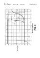
- FIG. 5 is a graph of a normalized signal and an end bit signal for the two plasma powers of FIG. 3 .
- FIG. 6 is a graph of an end bit signal compared with various gas “intensities” obtained by a residual gas analyzer (RGA).
- a PECVD apparatus 130 includes a susceptor 135 having a stem 137 .
- Susceptor 135 is centered within a vacuum deposition process chamber 133 .
- Susceptor 135 holds a substrate such as a glass panel (not shown) in a substrate processing or reaction region 141 .
- a lift mechanism (not shown) is provided to raise and lower the susceptor 135 . Commands to the lift mechanism are provided by a controller. Substrates are transferred into and out of chamber 133 through an opening 142 in a sidewall 134 of the chamber 133 by a robot blade (not shown).
- the deposition process gases flow into chamber 133 through a manifold 61 and an inlet 126 .
- the gases then flow through a perforated blocker plate 124 and a number of holes 121 in a process gas distribution faceplate 122 (indicated by small arrows in the substrate processing region 141 of FIG. 1 ).
- An RF power supply (not shown) may be used to apply electrical power between gas distribution faceplate 122 and susceptor 135 so as to excite the process gas mixture to form a plasma.
- the constituents of the plasma react to deposit a desired film on the surface of the substrate on susceptor 135 .
- the deposition process gases may be exhausted from the chamber through a slot-shaped orifice 131 surrounding substrate processing region 141 into an exhaust plenum 150 . From exhaust plenum 150 , the gases flow by a vacuum shut-off valve 154 and into an exhaust outlet 152 which connects to an external vacuum pump (not shown).
- a manometer 63 measures the total pressure of gases in chamber 133 .
- manometer 63 could be replaced by numerous other types of sensors for total pressure with equally good results.
- an ion gauge could be used.
- chamber 133 has at least an NF 3 gas supply 59 .
- Other gas supplies may also be used depending on the circumstances of the process.
- FIG. 2 also shows an argon (Ar) supply 57 .
- An optoelectronic endpoint detector 39 is provided which views the interior of chamber 113 through a window 38 .
- a first channel 33 having a first F* fiber 70 is used to detect the intensity of light emission at a fluorine emission line F* by filtering the chamber emission through a filter 34 . That is, like any atomic or molecular species, fluorine only absorbs and emits radiation at certain wavelengths. When a photon is emitted or absorbed, its energy corresponds to the difference between two permitted values of the energy of the atoms or molecules of the species. The energy levels may be studied by observing the differences between them. Each such difference corresponds to an “emission line.” The emission lines for any given species vary greatly in intensity.
- F* One characteristic emission of F* is at 704 nanometers (nm). The level of this emission may be continuously monitored with a photodetector which converts light intensity to an electrical signal. When the F* is reacting with the prior depositions (i.e., being consumed), the 704 nm emission intensity is low. When the prior depositions have been removed by cleaning, the F* emission level rises because there are few residues left with which the F* may react. The rise of F* thus denotes the end of the cleaning procedure, or its “endpoint.”
- the endpoint detector also has a second channel 35 , including background fiber 69 , for monitoring the total background light emission.
- a second channel 35 including background fiber 69 , for monitoring the total background light emission.
- the light Prior to or just after exiting fibers 69 and 70 , the light is passed through an appropriate filter so that either the F* emission is measured or the background emission is measured.
- the background light emission may be filtered with a broadband neutral density filter 32 .
- Filter 32 enables the second channel to measure background gas contributions that may be present at many different wavelengths, not just one wavelength in particular. That is, this type of filter includes contributions over a wide range of wavelengths.
- Fibers 69 and 70 transmit light signals from window 38 through filters 32 and 34 to a pair of standard photodetectors 30 . After measurement by photodetectors 30 , signals are sent corresponding to the amount of light intensity of either F* or the background.
- a normalized signal may be constructed by optoelectronically dividing the F* emission by the background emission using firmware and circuitry on a printed circuit board.
- firmware and circuitry on a printed circuit board.
- the printed circuit board and associated circuitry could be replaced by software to perform the same functions.
- the division described above is not the only workable algorithm. For example, subtraction or numerous other arithmetic functions could be performed on the signals to result in a normalized signal which could be used to monitor the endpoint.
- a requirement of this normalized signal is that its value should be substantially invariant with respect to simultaneous corresponding changes in the intensity of the signals measured by the first and second channels. For example, if the F* emission signal intensity and the background emission signal intensity both decrease due to deposition on the window facing the photodetectors or due to varying levels of applied RF power, the normalized signal value may stay substantially the same.
- Detector electronics 31 monitors this normalized signal in real time and determines when the normalized signal matches a threshold calibration signal obtained from a clean reference chamber.
- Hardware over-etch timer 68 institutes a waiting period in detector electronics 31 during which the value of the normalized signal is monitored and checked to ensure that it continues to exceed the calibration value. Hardware over-etch timer 68 serves to “desensitize” the endpoint to chamber fluctuations or anomalies. If detector electronics 31 finds that, during the hardware over-etch time, the normalized signal does not match a clean chamber, hardware over-etch timer 68 is reset.
- an additional signal which may be only a single bit, referred to here as a “done bit 67 ”, is sent to a cleaning program 55 signifying that the chamber is ready for subsequent steps in the cleaning program (e.g., further over-etch, seasoning, etc.).
- Detector electronics 31 may then be reset upon receipt of, e.g., an “enable bit” 72 .
- One further step may be performed by a software over-etch timer 71 .
- Software over-etch timer 71 is similar to the above hardware over-etch timer 68 , except that software over-etch timer 71 is instituted by the software of cleaning program 55 running on computer 50 .
- Software over-etch 71 timer may be run either with or without hardware over-etch 68 .
- chamber 133 may be cleaned.
- the user establishes a flow of gas into chamber 133 from which a plasma will be created.
- a flow of NF 3 is established. This may produce a range of pressures in chamber 133 of about 0.1 Torr to about 2.0 Torr, with a susceptor 135 -gas faceplate 122 spacing of about 500 mil to 2500 mil.
- the plasma of gases may be formed either in-situ in chamber 133 or ex-situ in a remote plasma chamber.
- gases from the remote plasma chamber enter chamber 133 from a separate valved inlet. More details of a remote plasma chamber may be found in U.S. patent application Ser. No. 08/707,491, filed Sep. 16, 1996, entitled “A Deposition Chamber Cleaning Technique Using a High Power Remote Excitation Source”, assigned to the assignee of the present invention and incorporated herein by reference.
- An RF power of about 1000 watts to about 4000 watts is applied to produce a plasma, corresponding to power densities of about 0.5 watts/cm 2 to about 3 watts/cm 2 of substrate area.
- Different deposited materials vary in the rates in which they may be cleaned or removed. For example, a plasma roughly within the energy range above cleans at a rate of about 3000 angstroms per minute to about 4000 angstroms per minute for a-Si, and at a rate of about 6000 angstroms per minute to about 7500 angstroms per minute for SiN.
- FIG. 3 shows this rise in the F* signal for a film consisting of three cycles of 3500 angstroms of silicon nitride and 600 angstroms of a-Si. This “rise” is actually a “drop” in FIG. 3 because the voltage signals are inverted on that figure and on FIGS. 4-5.
- FIG. 3 shows this rise in the F* signal for a film consisting of three cycles of 3500 angstroms of silicon nitride and 600 angstroms of a-Si. This “rise” is actually a “drop” in FIG. 3 because the voltage signals are inverted on that figure and on FIGS. 4-5.
- FIG. 3 shows this rise in the F* signal for a film consisting of three cycles of 3500 angstroms of silicon nitride and 600 angstroms of a-Si. This “rise” is actually a “drop” in FIG. 3 because the voltage signals are inverted on that figure and on FIGS. 4-5.
- FIG. 3 shows this rise in the
- FIG. 3 shows the photodiode preamplifier inverted voltage signals, which are measured by photodetectors 30 , for the 3000 watt 704 nm F* emission line signal 21 and for the background emission line signal 23 . These signals are shown as functions of time for two different values of applied plasma power, 3000 watts and 1500 watts (the 1500 watt curves are dotted; the 1500 watt F* line is shown as curve 22 , and the corresponding background line is curve 24 ). At about 50 seconds, F* signal 21 increases in intensity (for the case of the inverted preamplifier voltage, become more negative) until saturation. Because the F* signal 21 is increasing in intensity, the chamber pressure may be correspondingly increasing.
- the F* rise corresponds to a rise in chamber pressure to a range of about 0.25 Torr to about 0.45 Torr.
- the background emission signal 23 decreases (becomes less negative), until a saturation value is reached.
- the endpoint occurs when the two signals are each at saturation values (the saturation value for each signal is generally different).
- FIG. 3 shows that, regardless of plasma power, both sets of curves, 21 and 23 as well as 22 and 24 , saturate at the endpoint, which appears to occur at somewhere between 50 and 75 seconds.
- FIG. 4 shows the photodiode preamplifier inverted voltage signals as a function of time for a similar film, though this film's a-Si layer is only 500 angstroms thick.
- detector electronics 31 may be started which, as explained above, helps to ensure consistency of endpoint by eliminating spurious indications of endpoint due to pressure fluctuations, etc.
- This timer can be set by the user to be, e.g., 0, 2, 5, 10, or 15 sec.
- detector electronics 31 continues to check that normalized signal 25 is comparable to the threshold calibrated ratio. If the signals diverge, detector electronics 31 is reset to again wait for a proper signal matching.
- detector electronics 31 changes the state of done bit 67 from “asserted” to “unasserted” or “high” to “low”. In FIG. 4, this occurs at about 53 sec. The receipt of done bit 67 may in turn begin an additional software over-etch timer 71 in cleaning program 55 . Following the period of this timer, subsequent cleaning steps or processing steps may be performed.
- FIG. 5 shows the normalized signals for the data displayed in FIG. 3 where the cleaning method is used with two plasma powers.
- Curve 52 shows the normalized signal with a 3000 watt plasma and curve 54 shows the normalized signal with a 1500 watt plasma.
- Curve 54 is not as intense as curve 52 and the time to reach the endpoint is longer. Nevertheless, the level of the signal saturation is consistent. This shows that the method and apparatus of the invention can be advantageously used with plasmas of differing powers.
- the method and apparatus of the invention can be used even when the detector inputs are less efficient. For example, it is often the case that the transparency of window 38 separating the detectors from chamber 133 changes as deposited films inadvertently build-up on window 38 (this efficiency change acts similarly to a change in plasma power). This does not prevent the method and apparatus of the invention from being useful because the signal saturation may still be effectively detected despite the changing transparency of the window.
- FIG. 6 shows intensity signals measured on a residual gas analyzer (“RGA”) for the gas masses corresponding to fluorine (signal 62 ) and silicon fluoride (SiF 3 , signal 64 ). Done bit signal 66 from detector electronics 31 is also shown. Unlike the signals in FIGS. 3-5, these signals are not inverted.
- RAA residual gas analyzer
- RGA signals were measured as a check on the optoelectronic method discussed above.
- the y-axis has arbitrary units.
- the x-axis has units of seconds.
- the graph shows that fluorine signal 64 rises and silicon fluoride signal 62 falls such that they intersect at about 50 seconds. This intersection may be termed the “RGA endpoint”. This intersection occurred just prior to the signal saturation and done bit 66 assertion, which appears to occur at about 62 seconds. Thus, the RGA endpoint approximately agrees with that determined by detector electronics 31 .
- the precise point at which detector electronics 31 determined the endpoint is shown as a square dot 57 .
- Ar has been used as the inert gas and NF 3 the cleaning gas.
- Other inert, noble and molecular gases may also be used, such as helium, neon, krypton, xenon, and molecular nitrogen, as well as other gases with similar properties.
- other cleaning gases may also be used, such as CF 4 , C 2 F 6 , and SF 6 , as well as other gases with similar cleaning properties. Often these gases will contain fluorine.
- the cleaning method may be used to clean a number of deposited films.
- films of Si x O y , Si r N s , a-Si, polysilicon and SiON may all be removed by the invention.
Abstract
Description
Claims (15)
Priority Applications (9)
| Application Number | Priority Date | Filing Date | Title |
|---|---|---|---|
| US08/904,432 US6534007B1 (en) | 1997-08-01 | 1997-08-01 | Method and apparatus for detecting the endpoint of a chamber cleaning |
| JP2000505347A JP2001527151A (en) | 1997-08-01 | 1998-07-29 | Method and apparatus for detecting end point of chamber cleaning |
| KR1020007001118A KR20010022529A (en) | 1997-08-01 | 1998-07-29 | Method and apparatus for detecting the endpoint of a chamber cleaning |
| TW087112446A TW409289B (en) | 1997-08-01 | 1998-07-29 | Method and apparatus for detecting the endpoint of a chamber cleaning |
| KR1020067012434A KR20060083994A (en) | 1997-08-01 | 1998-07-29 | Method and apparatus for detecting the endpoint of a chamber cleaning |
| EP98937245A EP1007762B1 (en) | 1997-08-01 | 1998-07-29 | Method and apparatus for detecting the endpoint of a chamber cleaning |
| DE69830730T DE69830730T2 (en) | 1997-08-01 | 1998-07-29 | METHOD AND DEVICE FOR DETERMINING THE END POINT IN A CHAMBER CLEANING PROCESS |
| PCT/US1998/015705 WO1999006610A1 (en) | 1997-08-01 | 1998-07-29 | Method and apparatus for detecting the endpoint of a chamber cleaning |
| US10/393,311 US6881276B2 (en) | 1997-08-01 | 2003-03-18 | Detecting the endpoint of a chamber cleaning |
Applications Claiming Priority (1)
| Application Number | Priority Date | Filing Date | Title |
|---|---|---|---|
| US08/904,432 US6534007B1 (en) | 1997-08-01 | 1997-08-01 | Method and apparatus for detecting the endpoint of a chamber cleaning |
Related Child Applications (1)
| Application Number | Title | Priority Date | Filing Date |
|---|---|---|---|
| US10/393,311 Division US6881276B2 (en) | 1997-08-01 | 2003-03-18 | Detecting the endpoint of a chamber cleaning |
Publications (1)
| Publication Number | Publication Date |
|---|---|
| US6534007B1 true US6534007B1 (en) | 2003-03-18 |
Family
ID=25419158
Family Applications (2)
| Application Number | Title | Priority Date | Filing Date |
|---|---|---|---|
| US08/904,432 Expired - Fee Related US6534007B1 (en) | 1997-08-01 | 1997-08-01 | Method and apparatus for detecting the endpoint of a chamber cleaning |
| US10/393,311 Expired - Fee Related US6881276B2 (en) | 1997-08-01 | 2003-03-18 | Detecting the endpoint of a chamber cleaning |
Family Applications After (1)
| Application Number | Title | Priority Date | Filing Date |
|---|---|---|---|
| US10/393,311 Expired - Fee Related US6881276B2 (en) | 1997-08-01 | 2003-03-18 | Detecting the endpoint of a chamber cleaning |
Country Status (7)
| Country | Link |
|---|---|
| US (2) | US6534007B1 (en) |
| EP (1) | EP1007762B1 (en) |
| JP (1) | JP2001527151A (en) |
| KR (2) | KR20010022529A (en) |
| DE (1) | DE69830730T2 (en) |
| TW (1) | TW409289B (en) |
| WO (1) | WO1999006610A1 (en) |
Cited By (49)
| Publication number | Priority date | Publication date | Assignee | Title |
|---|---|---|---|---|
| US20030136425A1 (en) * | 2002-01-24 | 2003-07-24 | Applied Materials, Inc. | Process endpoint detection in processing chambers |
| US20030203626A1 (en) * | 2002-04-25 | 2003-10-30 | Derderian Garo J. | Apparatus and method for forming thin layers of materials on micro-device workpieces |
| US20030216041A1 (en) * | 2002-05-08 | 2003-11-20 | Herring Robert B. | In-situ thermal chamber cleaning |
| US20030219528A1 (en) * | 2002-05-24 | 2003-11-27 | Carpenter Craig M. | Apparatus and methods for controlling gas pulsing in processes for depositing materials onto micro-device workpieces |
| US20040000270A1 (en) * | 2002-06-26 | 2004-01-01 | Carpenter Craig M. | Methods and apparatus for vapor processing of micro-device workpieces |
| US20040003777A1 (en) * | 2002-07-08 | 2004-01-08 | Carpenter Craig M. | Apparatus and method for depositing materials onto microelectronic workpieces |
| US20040049908A1 (en) * | 2002-01-15 | 2004-03-18 | Quallion Llc | Electric storage battery construction and method of manufacture |
| US6716765B1 (en) * | 2002-11-12 | 2004-04-06 | Novellus Systems, Inc. | Plasma clean for a semiconductor thin film deposition chamber |
| US6758224B2 (en) * | 2001-01-22 | 2004-07-06 | Anelva Corporation | Method of cleaning CVD device |
| US20040226507A1 (en) * | 2003-04-24 | 2004-11-18 | Carpenter Craig M. | Methods for controlling mass flow rates and pressures in passageways coupled to reaction chambers and systems for depositing material onto microfeature workpieces in reaction chambers |
| US20040253828A1 (en) * | 2003-06-16 | 2004-12-16 | Takeshi Ozawa | Fabrication method of semiconductor integrated circuit device |
| US20050016984A1 (en) * | 2002-08-15 | 2005-01-27 | Dando Ross S. | Reactors with isolated gas connectors and methods for depositing materials onto micro-device workpieces |
| US20050039680A1 (en) * | 2003-08-21 | 2005-02-24 | Beaman Kevin L. | Methods and apparatus for processing microfeature workpieces; methods for conditioning ALD reaction chambers |
| US20050081786A1 (en) * | 2003-10-15 | 2005-04-21 | Kubista David J. | Systems for depositing material onto workpieces in reaction chambers and methods for removing byproducts from reaction chambers |
| US20050126489A1 (en) * | 2003-12-10 | 2005-06-16 | Beaman Kevin L. | Methods and systems for controlling temperature during microfeature workpiece processing, e.g., CVD deposition |
| US20050164466A1 (en) * | 2004-01-28 | 2005-07-28 | Zheng Lingyi A. | Methods for forming small-scale capacitor structures |
| US20050211264A1 (en) * | 2004-03-25 | 2005-09-29 | Tokyo Electron Limited Of Tbs Broadcast Center | Method and processing system for plasma-enhanced cleaning of system components |
| US20050241669A1 (en) * | 2004-04-29 | 2005-11-03 | Tokyo Electron Limited | Method and system of dry cleaning a processing chamber |
| US20050249873A1 (en) * | 2004-05-05 | 2005-11-10 | Demetrius Sarigiannis | Apparatuses and methods for producing chemically reactive vapors used in manufacturing microelectronic devices |
| US20050268856A1 (en) * | 2004-06-02 | 2005-12-08 | Miller Matthew W | Reactors, systems and methods for depositing thin films onto microfeature workpieces |
| US20060021633A1 (en) * | 2004-07-27 | 2006-02-02 | Applied Materials, Inc. | Closed loop clean gas control |
| US20060054183A1 (en) * | 2004-08-27 | 2006-03-16 | Thomas Nowak | Method to reduce plasma damage during cleaning of semiconductor wafer processing chamber |
| US20060090773A1 (en) * | 2004-11-04 | 2006-05-04 | Applied Materials, Inc. | Sulfur hexafluoride remote plasma source clean |
| US20060107973A1 (en) * | 2004-10-12 | 2006-05-25 | Samuel Leung | Endpoint detector and particle monitor |
| US20060115957A1 (en) * | 2003-09-17 | 2006-06-01 | Cem Basceri | Microfeature workpiece processing apparatus and methods for controlling deposition of materials on microfeature workpieces |
| US20060165873A1 (en) * | 2005-01-25 | 2006-07-27 | Micron Technology, Inc. | Plasma detection and associated systems and methods for controlling microfeature workpiece deposition processes |
| US20060198955A1 (en) * | 2003-08-21 | 2006-09-07 | Micron Technology, Inc. | Microfeature workpiece processing apparatus and methods for batch deposition of materials on microfeature workpieces |
| US20060205187A1 (en) * | 2003-08-28 | 2006-09-14 | Micron Technology, Inc. | Methods and apparatus for processing microfeature workpieces, e.g., for depositing materials on microfeature workpieces |
| US20060237138A1 (en) * | 2005-04-26 | 2006-10-26 | Micron Technology, Inc. | Apparatuses and methods for supporting microelectronic devices during plasma-based fabrication processes |
| US20070020776A1 (en) * | 2001-10-24 | 2007-01-25 | Tokyo Electron Limited | Method and apparatus for wall film monitoring |
| US20070221622A1 (en) * | 2004-03-25 | 2007-09-27 | Kim Nam H | Plasma Chamber Having Plasma Source Coil and Method for Etching the Wafer Using the Same |
| US20080047579A1 (en) * | 2006-08-25 | 2008-02-28 | Bing Ji | Detecting the endpoint of a cleaning process |
| US20080191153A1 (en) * | 2005-03-16 | 2008-08-14 | Advanced Technology Materials, Inc. | System For Delivery Of Reagents From Solid Sources Thereof |
| US7479191B1 (en) | 2005-04-22 | 2009-01-20 | Novellus Systems, Inc. | Method for endpointing CVD chamber cleans following ultra low-k film treatments |
| US20090095713A1 (en) * | 2004-10-26 | 2009-04-16 | Advanced Technology Materials, Inc. | Novel methods for cleaning ion implanter components |
| US20090151639A1 (en) * | 2001-08-01 | 2009-06-18 | Shigeru Kasai | Gas processing apparatus and gas processing method |
| US20090242511A1 (en) * | 2006-03-10 | 2009-10-01 | Mitsubishi Heavy Industries, Ltd. | Seasoning method for film-forming apparatus |
| US20100112191A1 (en) * | 2008-10-30 | 2010-05-06 | Micron Technology, Inc. | Systems and associated methods for depositing materials |
| US7727906B1 (en) | 2006-07-26 | 2010-06-01 | Novellus Systems, Inc. | H2-based plasma treatment to eliminate within-batch and batch-to-batch etch drift |
| US20100154835A1 (en) * | 2006-04-26 | 2010-06-24 | Advanced Technology Materials, Inc. | Cleaning of semiconductor processing systems |
| US20100166980A1 (en) * | 2008-12-26 | 2010-07-01 | Canon Anelva Corporation | Inline vacuum processing apparatus, method of controlling the same, and information recording medium manufacturing method |
| US8133554B2 (en) | 2004-05-06 | 2012-03-13 | Micron Technology, Inc. | Methods for depositing material onto microfeature workpieces in reaction chambers and systems for depositing materials onto microfeature workpieces |
| US8262800B1 (en) | 2008-02-12 | 2012-09-11 | Novellus Systems, Inc. | Methods and apparatus for cleaning deposition reactors |
| US8591659B1 (en) | 2009-01-16 | 2013-11-26 | Novellus Systems, Inc. | Plasma clean method for deposition chamber |
| US9991095B2 (en) | 2008-02-11 | 2018-06-05 | Entegris, Inc. | Ion source cleaning in semiconductor processing systems |
| US9997325B2 (en) | 2008-07-17 | 2018-06-12 | Verity Instruments, Inc. | Electron beam exciter for use in chemical analysis in processing systems |
| US20200176233A1 (en) * | 2018-11-30 | 2020-06-04 | Applied Materials, Inc. | In-situ real-time plasma chamber condition monitoring |
| WO2021091780A1 (en) * | 2019-11-04 | 2021-05-14 | Applied Materials, Inc. | Optical absorption sensor for semiconductor processing |
| US20230187190A1 (en) * | 2019-03-25 | 2023-06-15 | Atonarp Inc. | Gas analyzer apparatus |
Families Citing this family (19)
| Publication number | Priority date | Publication date | Assignee | Title |
|---|---|---|---|---|
| US6366346B1 (en) * | 1998-11-19 | 2002-04-02 | Applied Materials, Inc. | Method and apparatus for optical detection of effluent composition |
| KR100844273B1 (en) * | 2002-12-20 | 2008-07-07 | 동부일렉트로닉스 주식회사 | Chamber cleaner |
| CN101457338B (en) * | 2003-02-14 | 2011-04-27 | 应用材料股份有限公司 | Cleaning of native oxide with hydrogen-containing radicals |
| JP4385086B2 (en) | 2003-03-14 | 2009-12-16 | パナソニック株式会社 | CVD apparatus cleaning apparatus and CVD apparatus cleaning method |
| US20060006139A1 (en) * | 2003-05-09 | 2006-01-12 | David Johnson | Selection of wavelengths for end point in a time division multiplexed process |
| KR100997964B1 (en) * | 2003-06-16 | 2010-12-02 | 삼성전자주식회사 | Manufacturing method of thin film transistor array panel |
| US20060162742A1 (en) * | 2005-01-26 | 2006-07-27 | Tokyo Electron Limited | Cleaning method of processing apparatus, program for performing the method, and storage medium for storing the program |
| US9627184B2 (en) * | 2005-01-26 | 2017-04-18 | Tokyo Electron Limited | Cleaning method of processing apparatus, program for performing the method, and storage medium for storing the program |
| JP2006339253A (en) * | 2005-05-31 | 2006-12-14 | Toshiba Corp | Plasma processing device and method |
| US20070074741A1 (en) * | 2005-09-30 | 2007-04-05 | Tokyo Electron Limited | Method for dry cleaning nickel deposits from a processing system |
| US7550090B2 (en) * | 2007-01-23 | 2009-06-23 | Applied Materials, Inc. | Oxygen plasma clean to remove carbon species deposited on a glass dome surface |
| JP5281766B2 (en) | 2007-07-31 | 2013-09-04 | ルネサスエレクトロニクス株式会社 | Manufacturing method of semiconductor integrated circuit device |
| US8158017B2 (en) * | 2008-05-12 | 2012-04-17 | Lam Research Corporation | Detection of arcing events in wafer plasma processing through monitoring of trace gas concentrations |
| US10043641B2 (en) | 2016-09-22 | 2018-08-07 | Applied Materials, Inc. | Methods and apparatus for processing chamber cleaning end point detection |
| KR102017559B1 (en) * | 2017-10-17 | 2019-09-03 | 주식회사 프라임솔루션 | A Process Monitoring Equipment Having Calibration Lamp And Method Of Process Monitoring Method Using The Same |
| CN109731856A (en) * | 2018-12-29 | 2019-05-10 | 广东晶科电子股份有限公司 | A kind of detection system of LED support plasma cleaning process |
| US11398520B2 (en) * | 2019-01-11 | 2022-07-26 | HKC Corporation Limited | X-ray detector, method for manufacturing x-ray detector, and medical equipment |
| WO2021025819A1 (en) * | 2019-08-06 | 2021-02-11 | Applied Materials, Inc. | Methods for detection using optical emission spectroscopy |
| US20240055230A1 (en) * | 2022-08-15 | 2024-02-15 | Applied Materials, Inc. | System and method of cleaning process chamber components |
Citations (18)
| Publication number | Priority date | Publication date | Assignee | Title |
|---|---|---|---|---|
| US4289188A (en) * | 1979-05-28 | 1981-09-15 | Hitachi, Ltd. | Method and apparatus for monitoring etching |
| US4430151A (en) * | 1982-06-11 | 1984-02-07 | Anelva Corporation | Method of monitoring status of a silicon layer by detecting, emission spectra variable during etching |
| US4491499A (en) * | 1984-03-29 | 1985-01-01 | At&T Technologies, Inc. | Optical emission end point detector |
| US4657620A (en) * | 1984-10-22 | 1987-04-14 | Texas Instruments Incorporated | Automated single slice powered load lock plasma reactor |
| US5045149A (en) * | 1988-10-24 | 1991-09-03 | Vlsi Technology, Inc. | Method and apparatus for end point detection |
| JPH04152550A (en) | 1990-10-16 | 1992-05-26 | Oki Electric Ind Co Ltd | Manufacture of semiconductor device |
| US5160402A (en) * | 1990-05-24 | 1992-11-03 | Applied Materials, Inc. | Multi-channel plasma discharge endpoint detection method |
| US5290383A (en) * | 1991-03-24 | 1994-03-01 | Tokyo Electron Limited | Plasma-process system with improved end-point detecting scheme |
| US5308414A (en) | 1992-12-23 | 1994-05-03 | International Business Machines Corporation | Method and apparatus for optical emission end point detection in plasma etching processes |
| US5320704A (en) * | 1990-11-28 | 1994-06-14 | Tokyo Electron Limited | Plasma etching apparatus |
| US5348614A (en) | 1993-06-22 | 1994-09-20 | Lsi Logic Corporation | Process for dynamic control of the concentration of one or more reactants in a plasma-enhanced process for formation of integrated circuit structures |
| US5352902A (en) * | 1992-07-06 | 1994-10-04 | Tokyo Electron Kabushiki Kaisha | Method for controlling plasma surface-treatments with a plurality of photodetectors and optical filters |
| US5356478A (en) * | 1992-06-22 | 1994-10-18 | Lam Research Corporation | Plasma cleaning method for removing residues in a plasma treatment chamber |
| US5552016A (en) | 1993-04-28 | 1996-09-03 | Applied Materials, Inc. | Method and apparatus for etchback endpoint detection |
| US5565114A (en) * | 1993-03-04 | 1996-10-15 | Tokyo Electron Limited | Method and device for detecting the end point of plasma process |
| US5632821A (en) | 1995-03-03 | 1997-05-27 | Anelva Corporation | Post treatment method for in-situ cleaning |
| US5643364A (en) | 1994-11-30 | 1997-07-01 | Applied Materials, Inc. | Plasma chamber with fixed RF matching |
| US5812403A (en) | 1996-11-13 | 1998-09-22 | Applied Materials, Inc. | Methods and apparatus for cleaning surfaces in a substrate processing system |
Family Cites Families (1)
| Publication number | Priority date | Publication date | Assignee | Title |
|---|---|---|---|---|
| GB8823669D0 (en) * | 1988-10-08 | 1988-11-16 | Thackray C F Ltd | Surgical instrument |
-
1997
- 1997-08-01 US US08/904,432 patent/US6534007B1/en not_active Expired - Fee Related
-
1998
- 1998-07-29 DE DE69830730T patent/DE69830730T2/en not_active Expired - Fee Related
- 1998-07-29 EP EP98937245A patent/EP1007762B1/en not_active Expired - Lifetime
- 1998-07-29 TW TW087112446A patent/TW409289B/en not_active IP Right Cessation
- 1998-07-29 WO PCT/US1998/015705 patent/WO1999006610A1/en not_active Application Discontinuation
- 1998-07-29 KR KR1020007001118A patent/KR20010022529A/en not_active Application Discontinuation
- 1998-07-29 KR KR1020067012434A patent/KR20060083994A/en not_active Application Discontinuation
- 1998-07-29 JP JP2000505347A patent/JP2001527151A/en active Pending
-
2003
- 2003-03-18 US US10/393,311 patent/US6881276B2/en not_active Expired - Fee Related
Patent Citations (19)
| Publication number | Priority date | Publication date | Assignee | Title |
|---|---|---|---|---|
| US4289188A (en) * | 1979-05-28 | 1981-09-15 | Hitachi, Ltd. | Method and apparatus for monitoring etching |
| US4430151A (en) * | 1982-06-11 | 1984-02-07 | Anelva Corporation | Method of monitoring status of a silicon layer by detecting, emission spectra variable during etching |
| US4491499A (en) * | 1984-03-29 | 1985-01-01 | At&T Technologies, Inc. | Optical emission end point detector |
| US4657620A (en) * | 1984-10-22 | 1987-04-14 | Texas Instruments Incorporated | Automated single slice powered load lock plasma reactor |
| US5045149A (en) * | 1988-10-24 | 1991-09-03 | Vlsi Technology, Inc. | Method and apparatus for end point detection |
| US5160402A (en) * | 1990-05-24 | 1992-11-03 | Applied Materials, Inc. | Multi-channel plasma discharge endpoint detection method |
| JPH04152550A (en) | 1990-10-16 | 1992-05-26 | Oki Electric Ind Co Ltd | Manufacture of semiconductor device |
| US5320704A (en) * | 1990-11-28 | 1994-06-14 | Tokyo Electron Limited | Plasma etching apparatus |
| US5290383A (en) * | 1991-03-24 | 1994-03-01 | Tokyo Electron Limited | Plasma-process system with improved end-point detecting scheme |
| US5322590A (en) * | 1991-03-24 | 1994-06-21 | Tokyo Electron Limited | Plasma-process system with improved end-point detecting scheme |
| US5356478A (en) * | 1992-06-22 | 1994-10-18 | Lam Research Corporation | Plasma cleaning method for removing residues in a plasma treatment chamber |
| US5352902A (en) * | 1992-07-06 | 1994-10-04 | Tokyo Electron Kabushiki Kaisha | Method for controlling plasma surface-treatments with a plurality of photodetectors and optical filters |
| US5308414A (en) | 1992-12-23 | 1994-05-03 | International Business Machines Corporation | Method and apparatus for optical emission end point detection in plasma etching processes |
| US5565114A (en) * | 1993-03-04 | 1996-10-15 | Tokyo Electron Limited | Method and device for detecting the end point of plasma process |
| US5552016A (en) | 1993-04-28 | 1996-09-03 | Applied Materials, Inc. | Method and apparatus for etchback endpoint detection |
| US5348614A (en) | 1993-06-22 | 1994-09-20 | Lsi Logic Corporation | Process for dynamic control of the concentration of one or more reactants in a plasma-enhanced process for formation of integrated circuit structures |
| US5643364A (en) | 1994-11-30 | 1997-07-01 | Applied Materials, Inc. | Plasma chamber with fixed RF matching |
| US5632821A (en) | 1995-03-03 | 1997-05-27 | Anelva Corporation | Post treatment method for in-situ cleaning |
| US5812403A (en) | 1996-11-13 | 1998-09-22 | Applied Materials, Inc. | Methods and apparatus for cleaning surfaces in a substrate processing system |
Cited By (81)
| Publication number | Priority date | Publication date | Assignee | Title |
|---|---|---|---|---|
| US6758224B2 (en) * | 2001-01-22 | 2004-07-06 | Anelva Corporation | Method of cleaning CVD device |
| US20080276957A1 (en) * | 2001-01-22 | 2008-11-13 | Anelva Corporation | Method of cleaning a cvd device |
| US8105440B2 (en) | 2001-01-22 | 2012-01-31 | Canon Anelva Corporation | Method of cleaning a CVD device |
| US20040194708A1 (en) * | 2001-01-22 | 2004-10-07 | Anelva Corporation | Method of cleaning a cvd device |
| US20090151639A1 (en) * | 2001-08-01 | 2009-06-18 | Shigeru Kasai | Gas processing apparatus and gas processing method |
| US20070020776A1 (en) * | 2001-10-24 | 2007-01-25 | Tokyo Electron Limited | Method and apparatus for wall film monitoring |
| US7732227B2 (en) * | 2001-10-24 | 2010-06-08 | Tokyo Electron Limited | Method and apparatus for wall film monitoring |
| US20040049908A1 (en) * | 2002-01-15 | 2004-03-18 | Quallion Llc | Electric storage battery construction and method of manufacture |
| US6878214B2 (en) | 2002-01-24 | 2005-04-12 | Applied Materials, Inc. | Process endpoint detection in processing chambers |
| US20030136425A1 (en) * | 2002-01-24 | 2003-07-24 | Applied Materials, Inc. | Process endpoint detection in processing chambers |
| US20030203626A1 (en) * | 2002-04-25 | 2003-10-30 | Derderian Garo J. | Apparatus and method for forming thin layers of materials on micro-device workpieces |
| US20050145337A1 (en) * | 2002-04-25 | 2005-07-07 | Derderian Garo J. | Apparatus for forming thin layers of materials on micro-device workpieces |
| US6861094B2 (en) | 2002-04-25 | 2005-03-01 | Micron Technology, Inc. | Methods for forming thin layers of materials on micro-device workpieces |
| US20030216041A1 (en) * | 2002-05-08 | 2003-11-20 | Herring Robert B. | In-situ thermal chamber cleaning |
| US20030219528A1 (en) * | 2002-05-24 | 2003-11-27 | Carpenter Craig M. | Apparatus and methods for controlling gas pulsing in processes for depositing materials onto micro-device workpieces |
| US6838114B2 (en) | 2002-05-24 | 2005-01-04 | Micron Technology, Inc. | Methods for controlling gas pulsing in processes for depositing materials onto micro-device workpieces |
| US7118783B2 (en) | 2002-06-26 | 2006-10-10 | Micron Technology, Inc. | Methods and apparatus for vapor processing of micro-device workpieces |
| US20070020394A1 (en) * | 2002-06-26 | 2007-01-25 | Micron Technology, Inc. | Methods and apparatus for vapor processing of micro-device workpieces |
| US20040000270A1 (en) * | 2002-06-26 | 2004-01-01 | Carpenter Craig M. | Methods and apparatus for vapor processing of micro-device workpieces |
| US20040003777A1 (en) * | 2002-07-08 | 2004-01-08 | Carpenter Craig M. | Apparatus and method for depositing materials onto microelectronic workpieces |
| US6821347B2 (en) | 2002-07-08 | 2004-11-23 | Micron Technology, Inc. | Apparatus and method for depositing materials onto microelectronic workpieces |
| US20050133161A1 (en) * | 2002-07-08 | 2005-06-23 | Carpenter Craig M. | Apparatus and method for depositing materials onto microelectronic workpieces |
| US20050022739A1 (en) * | 2002-07-08 | 2005-02-03 | Carpenter Craig M. | Apparatus and method for depositing materials onto microelectronic workpieces |
| US20050016984A1 (en) * | 2002-08-15 | 2005-01-27 | Dando Ross S. | Reactors with isolated gas connectors and methods for depositing materials onto micro-device workpieces |
| US6716765B1 (en) * | 2002-11-12 | 2004-04-06 | Novellus Systems, Inc. | Plasma clean for a semiconductor thin film deposition chamber |
| US20040226507A1 (en) * | 2003-04-24 | 2004-11-18 | Carpenter Craig M. | Methods for controlling mass flow rates and pressures in passageways coupled to reaction chambers and systems for depositing material onto microfeature workpieces in reaction chambers |
| US20080318429A1 (en) * | 2003-06-16 | 2008-12-25 | Takeshi Ozawa | Fabrication method of semiconductor integrated circuit device |
| US20080233761A1 (en) * | 2003-06-16 | 2008-09-25 | Takeshi Ozawa | Fabrication method of semiconductor integrated circuit device |
| US20040253828A1 (en) * | 2003-06-16 | 2004-12-16 | Takeshi Ozawa | Fabrication method of semiconductor integrated circuit device |
| US20050039680A1 (en) * | 2003-08-21 | 2005-02-24 | Beaman Kevin L. | Methods and apparatus for processing microfeature workpieces; methods for conditioning ALD reaction chambers |
| US20060198955A1 (en) * | 2003-08-21 | 2006-09-07 | Micron Technology, Inc. | Microfeature workpiece processing apparatus and methods for batch deposition of materials on microfeature workpieces |
| US20060205187A1 (en) * | 2003-08-28 | 2006-09-14 | Micron Technology, Inc. | Methods and apparatus for processing microfeature workpieces, e.g., for depositing materials on microfeature workpieces |
| US20060115957A1 (en) * | 2003-09-17 | 2006-06-01 | Cem Basceri | Microfeature workpiece processing apparatus and methods for controlling deposition of materials on microfeature workpieces |
| US20050081786A1 (en) * | 2003-10-15 | 2005-04-21 | Kubista David J. | Systems for depositing material onto workpieces in reaction chambers and methods for removing byproducts from reaction chambers |
| US7647886B2 (en) | 2003-10-15 | 2010-01-19 | Micron Technology, Inc. | Systems for depositing material onto workpieces in reaction chambers and methods for removing byproducts from reaction chambers |
| US20050126489A1 (en) * | 2003-12-10 | 2005-06-16 | Beaman Kevin L. | Methods and systems for controlling temperature during microfeature workpiece processing, e.g., CVD deposition |
| US7771537B2 (en) | 2003-12-10 | 2010-08-10 | Micron Technology, Inc. | Methods and systems for controlling temperature during microfeature workpiece processing, E.G. CVD deposition |
| US8518184B2 (en) | 2003-12-10 | 2013-08-27 | Micron Technology, Inc. | Methods and systems for controlling temperature during microfeature workpiece processing, E.G., CVD deposition |
| US20060204649A1 (en) * | 2003-12-10 | 2006-09-14 | Micron Technology, Inc. | Methods and systems for controlling temperature during microfeature workpiece processing, E.G. CVD deposition |
| US7906393B2 (en) | 2004-01-28 | 2011-03-15 | Micron Technology, Inc. | Methods for forming small-scale capacitor structures |
| US20050164466A1 (en) * | 2004-01-28 | 2005-07-28 | Zheng Lingyi A. | Methods for forming small-scale capacitor structures |
| US8384192B2 (en) | 2004-01-28 | 2013-02-26 | Micron Technology, Inc. | Methods for forming small-scale capacitor structures |
| WO2005104186A2 (en) * | 2004-03-25 | 2005-11-03 | Tokyo Electron Limited | Method and processing system for plasma-enhanced cleaning of system components |
| US20050211264A1 (en) * | 2004-03-25 | 2005-09-29 | Tokyo Electron Limited Of Tbs Broadcast Center | Method and processing system for plasma-enhanced cleaning of system components |
| US7524395B2 (en) | 2004-03-25 | 2009-04-28 | Adaptive Plasma Technology Corp. | Plasma chamber having plasma source coil and method for etching the wafer using the same |
| US20070221622A1 (en) * | 2004-03-25 | 2007-09-27 | Kim Nam H | Plasma Chamber Having Plasma Source Coil and Method for Etching the Wafer Using the Same |
| WO2005104186A3 (en) * | 2004-03-25 | 2006-08-17 | Tokyo Electron Ltd | Method and processing system for plasma-enhanced cleaning of system components |
| US20050241669A1 (en) * | 2004-04-29 | 2005-11-03 | Tokyo Electron Limited | Method and system of dry cleaning a processing chamber |
| US20050249873A1 (en) * | 2004-05-05 | 2005-11-10 | Demetrius Sarigiannis | Apparatuses and methods for producing chemically reactive vapors used in manufacturing microelectronic devices |
| US8133554B2 (en) | 2004-05-06 | 2012-03-13 | Micron Technology, Inc. | Methods for depositing material onto microfeature workpieces in reaction chambers and systems for depositing materials onto microfeature workpieces |
| US9023436B2 (en) | 2004-05-06 | 2015-05-05 | Micron Technology, Inc. | Methods for depositing material onto microfeature workpieces in reaction chambers and systems for depositing materials onto microfeature workpieces |
| US20050268856A1 (en) * | 2004-06-02 | 2005-12-08 | Miller Matthew W | Reactors, systems and methods for depositing thin films onto microfeature workpieces |
| US7699932B2 (en) | 2004-06-02 | 2010-04-20 | Micron Technology, Inc. | Reactors, systems and methods for depositing thin films onto microfeature workpieces |
| US20060021633A1 (en) * | 2004-07-27 | 2006-02-02 | Applied Materials, Inc. | Closed loop clean gas control |
| US20060054183A1 (en) * | 2004-08-27 | 2006-03-16 | Thomas Nowak | Method to reduce plasma damage during cleaning of semiconductor wafer processing chamber |
| US20060107973A1 (en) * | 2004-10-12 | 2006-05-25 | Samuel Leung | Endpoint detector and particle monitor |
| US20090095713A1 (en) * | 2004-10-26 | 2009-04-16 | Advanced Technology Materials, Inc. | Novel methods for cleaning ion implanter components |
| US20060090773A1 (en) * | 2004-11-04 | 2006-05-04 | Applied Materials, Inc. | Sulfur hexafluoride remote plasma source clean |
| US20060165873A1 (en) * | 2005-01-25 | 2006-07-27 | Micron Technology, Inc. | Plasma detection and associated systems and methods for controlling microfeature workpiece deposition processes |
| US20080191153A1 (en) * | 2005-03-16 | 2008-08-14 | Advanced Technology Materials, Inc. | System For Delivery Of Reagents From Solid Sources Thereof |
| US7479191B1 (en) | 2005-04-22 | 2009-01-20 | Novellus Systems, Inc. | Method for endpointing CVD chamber cleans following ultra low-k film treatments |
| US20060237138A1 (en) * | 2005-04-26 | 2006-10-26 | Micron Technology, Inc. | Apparatuses and methods for supporting microelectronic devices during plasma-based fabrication processes |
| US20090242511A1 (en) * | 2006-03-10 | 2009-10-01 | Mitsubishi Heavy Industries, Ltd. | Seasoning method for film-forming apparatus |
| US8337960B2 (en) | 2006-03-10 | 2012-12-25 | Mitsubishi Heavy Industries, Ltd. | Seasoning method for film-forming apparatus |
| US8603252B2 (en) * | 2006-04-26 | 2013-12-10 | Advanced Technology Materials, Inc. | Cleaning of semiconductor processing systems |
| US20100154835A1 (en) * | 2006-04-26 | 2010-06-24 | Advanced Technology Materials, Inc. | Cleaning of semiconductor processing systems |
| US7727906B1 (en) | 2006-07-26 | 2010-06-01 | Novellus Systems, Inc. | H2-based plasma treatment to eliminate within-batch and batch-to-batch etch drift |
| US20080047579A1 (en) * | 2006-08-25 | 2008-02-28 | Bing Ji | Detecting the endpoint of a cleaning process |
| US9991095B2 (en) | 2008-02-11 | 2018-06-05 | Entegris, Inc. | Ion source cleaning in semiconductor processing systems |
| US8262800B1 (en) | 2008-02-12 | 2012-09-11 | Novellus Systems, Inc. | Methods and apparatus for cleaning deposition reactors |
| US9997325B2 (en) | 2008-07-17 | 2018-06-12 | Verity Instruments, Inc. | Electron beam exciter for use in chemical analysis in processing systems |
| US20100112191A1 (en) * | 2008-10-30 | 2010-05-06 | Micron Technology, Inc. | Systems and associated methods for depositing materials |
| US8900363B2 (en) * | 2008-12-26 | 2014-12-02 | Canon Anelva Corporation | Inline vacuum processing apparatus, method of controlling the same, and information recording medium manufacturing method |
| US20100166980A1 (en) * | 2008-12-26 | 2010-07-01 | Canon Anelva Corporation | Inline vacuum processing apparatus, method of controlling the same, and information recording medium manufacturing method |
| US8591659B1 (en) | 2009-01-16 | 2013-11-26 | Novellus Systems, Inc. | Plasma clean method for deposition chamber |
| US20200176233A1 (en) * | 2018-11-30 | 2020-06-04 | Applied Materials, Inc. | In-situ real-time plasma chamber condition monitoring |
| US10854433B2 (en) * | 2018-11-30 | 2020-12-01 | Applied Materials, Inc. | In-situ real-time plasma chamber condition monitoring |
| US20230187190A1 (en) * | 2019-03-25 | 2023-06-15 | Atonarp Inc. | Gas analyzer apparatus |
| US11942312B2 (en) * | 2019-03-25 | 2024-03-26 | Atonarp Inc. | Gas analyzer apparatus |
| WO2021091780A1 (en) * | 2019-11-04 | 2021-05-14 | Applied Materials, Inc. | Optical absorption sensor for semiconductor processing |
| US11848178B2 (en) | 2019-11-04 | 2023-12-19 | Applied Materials, Inc. | Optical absorption sensor for semiconductor processing |
Also Published As
| Publication number | Publication date |
|---|---|
| JP2001527151A (en) | 2001-12-25 |
| WO1999006610A1 (en) | 1999-02-11 |
| US6881276B2 (en) | 2005-04-19 |
| TW409289B (en) | 2000-10-21 |
| KR20060083994A (en) | 2006-07-21 |
| EP1007762A1 (en) | 2000-06-14 |
| KR20010022529A (en) | 2001-03-15 |
| EP1007762B1 (en) | 2005-06-29 |
| DE69830730T2 (en) | 2006-05-04 |
| US20030159711A1 (en) | 2003-08-28 |
| DE69830730D1 (en) | 2005-08-04 |
Similar Documents
| Publication | Publication Date | Title |
|---|---|---|
| US6534007B1 (en) | Method and apparatus for detecting the endpoint of a chamber cleaning | |
| KR100767804B1 (en) | A method and device for controlling a cleaning cycle | |
| US7067432B2 (en) | Methodology for in-situ and real-time chamber condition monitoring and process recovery during plasma processing | |
| KR100521109B1 (en) | Processing apparatus and cleaning method | |
| KR100881045B1 (en) | Duo-step plasma cleaning of chamber residues | |
| US6366346B1 (en) | Method and apparatus for optical detection of effluent composition | |
| O’Neill et al. | Role of the chamber wall in low‐pressure high‐density etching plasmas | |
| US6815362B1 (en) | End point determination of process residues in wafer-less auto clean process using optical emission spectroscopy | |
| JP4801045B2 (en) | Method for removing chamber residue from a plasma processing system in a dry cleaning process | |
| US20030005943A1 (en) | High pressure wafer-less auto clean for etch applications | |
| US6124927A (en) | Method to protect chamber wall from etching by endpoint plasma clean | |
| US6919279B1 (en) | Endpoint detection for high density plasma (HDP) processes | |
| JP2781545B2 (en) | Semiconductor manufacturing equipment | |
| JP3333657B2 (en) | Vapor phase etching apparatus and vapor phase etching method | |
| KR20100123866A (en) | Effluent impedance based endpoint detection | |
| JP3231560B2 (en) | Plasma etching equipment | |
| WO1999006611A1 (en) | Method and apparatus for chamber cleaning | |
| JPH0343775B2 (en) | ||
| JP2005019763A (en) | Dry etching device | |
| JPH08148475A (en) | Etching processing device | |
| JPS627274B2 (en) | ||
| JPH0997785A (en) | Plasma processing device and plasma cleaning method | |
| JPS60253229A (en) | Optical window for plasma etching device |
Legal Events
| Date | Code | Title | Description |
|---|---|---|---|
| AS | Assignment |
Owner name: APPLIED MATERIALS, INC., CALIFORNIA Free format text: ASSIGNMENT OF ASSIGNORS INTEREST;ASSIGNORS:BLONIGAN, WENDELL T.;GARDNER, JAMES T.;REEL/FRAME:009166/0654;SIGNING DATES FROM 19971105 TO 19971201 |
|
| AS | Assignment |
Owner name: APPLIED KOMATSU TECHNOLOGY, INC., JAPAN Free format text: ASSIGNMENT OF ASSIGNORS INTEREST;ASSIGNORS:BLONIGAN, WENDELL T.;GARDNER, JAMES T.;REEL/FRAME:012202/0730;SIGNING DATES FROM 19971105 TO 19971201 |
|
| AS | Assignment |
Owner name: APPLIED KOMATSU TECHNOLOGY INC, JAPAN Free format text: ASSIGNMENT OF ASSIGNORS INTEREST;ASSIGNORS:BLONIGAN, WENDELL T.;GARDNER, JAMES T.;REEL/FRAME:012656/0207;SIGNING DATES FROM 19971105 TO 19971201 |
|
| FPAY | Fee payment |
Year of fee payment: 4 |
|
| FPAY | Fee payment |
Year of fee payment: 8 |
|
| REMI | Maintenance fee reminder mailed | ||
| LAPS | Lapse for failure to pay maintenance fees | ||
| STCH | Information on status: patent discontinuation |
Free format text: PATENT EXPIRED DUE TO NONPAYMENT OF MAINTENANCE FEES UNDER 37 CFR 1.362 |
|
| FP | Lapsed due to failure to pay maintenance fee |
Effective date: 20150318 |