US6522185B2 - Variable delay CMOS circuit with PVT control - Google Patents
Variable delay CMOS circuit with PVT control Download PDFInfo
- Publication number
- US6522185B2 US6522185B2 US09/796,306 US79630601A US6522185B2 US 6522185 B2 US6522185 B2 US 6522185B2 US 79630601 A US79630601 A US 79630601A US 6522185 B2 US6522185 B2 US 6522185B2
- Authority
- US
- United States
- Prior art keywords
- signal
- binary input
- delayed
- circuit recited
- gate
- Prior art date
- Legal status (The legal status is an assumption and is not a legal conclusion. Google has not performed a legal analysis and makes no representation as to the accuracy of the status listed.)
- Expired - Lifetime
Links
Images


Classifications
-
- H—ELECTRICITY
- H03—ELECTRONIC CIRCUITRY
- H03K—PULSE TECHNIQUE
- H03K5/00—Manipulating of pulses not covered by one of the other main groups of this subclass
- H03K5/13—Arrangements having a single output and transforming input signals into pulses delivered at desired time intervals
- H03K5/133—Arrangements having a single output and transforming input signals into pulses delivered at desired time intervals using a chain of active delay devices
-
- H—ELECTRICITY
- H03—ELECTRONIC CIRCUITRY
- H03H—IMPEDANCE NETWORKS, e.g. RESONANT CIRCUITS; RESONATORS
- H03H11/00—Networks using active elements
- H03H11/02—Multiple-port networks
- H03H11/26—Time-delay networks
- H03H11/265—Time-delay networks with adjustable delay
-
- H—ELECTRICITY
- H03—ELECTRONIC CIRCUITRY
- H03K—PULSE TECHNIQUE
- H03K5/00—Manipulating of pulses not covered by one of the other main groups of this subclass
- H03K2005/00013—Delay, i.e. output pulse is delayed after input pulse and pulse length of output pulse is dependent on pulse length of input pulse
- H03K2005/00019—Variable delay
- H03K2005/00026—Variable delay controlled by an analog electrical signal, e.g. obtained after conversion by a D/A converter
- H03K2005/00032—Dc control of switching transistors
- H03K2005/00039—Dc control of switching transistors having four transistors serially
-
- H—ELECTRICITY
- H03—ELECTRONIC CIRCUITRY
- H03K—PULSE TECHNIQUE
- H03K5/00—Manipulating of pulses not covered by one of the other main groups of this subclass
- H03K2005/00013—Delay, i.e. output pulse is delayed after input pulse and pulse length of output pulse is dependent on pulse length of input pulse
- H03K2005/00078—Fixed delay
Definitions
- the present disclosure is generally related to electronic digital logic circuitry affecting signal sensitivity or transmission integrity and, more particularly, to a method and apparatus for variably controlling the propagation delay of a binary signal.
- CMOS is an acronym for the Complementary Metal Oxide Semiconductor. As the name implies, CMOS devices are formed using metal conductors, oxide insulators, and “semiconductors.” Semiconductors are crystalline materials having electrical properties between that of a conductor and an insulator. The conductivity of semiconductor material can be precisely controlled in a process called “doping” where a small amount of “dopant” is added to an otherwise pure, or “intrinsic,” semiconductor material. Doping leaves behind mobile, charged carriers for conducting electricity in the otherwise electrically-neutral semiconductor crystal lattice.
- the material When intrinsic semiconductor materials are doped so as to add negative charge carriers to the lattice, the material is referred to as an “n-type,” or donor “extrinsic” semiconductor, while the addition of positive carriers creates a “p-type,” acceptor material.
- a “transistor” is one particular type of semiconductor device that is noteworthy for its ability to operate as an electrical switch or amplifier, depending upon its configuration.
- transistors bipolar (or junction) transistors and field-effect transistors (“FETs”).
- FETs field-effect transistors
- field-effect is related to the application of an “electromotive field,” or voltage, to a “gate” terminal connected near the “junction” of the p-type and n-type materials.
- This gate voltage controls the size of a conductive “channel” through which electrons must flow through as they pass from the “source” terminal to the “drain” terminal, or vice versa. Consequently, the gate voltage can be used to control the source-drain current through the channel in an FET.
- MOSFETs Metal-oxide FETs, or “MOSFETs,” have an additional layer of a non-conductive oxide material (such as silicon dioxide) that insulates the gate terminal from the channel. Consequently, the gate current is very small regardless of the applied voltage so that circuits using MOSFETs can be made to consume, or “dissipate,” very little power.
- MOSFETs are characterized by their mode of operation and whether the channel is made from an n- or p-type semiconductor material. “Depletion-mode” operation occurs when the gate-source voltage (between the gate and source terminals) is used to deplete the channel of free carriers so as to reduce the size of the conductive channel and increase its resistance.
- Enhancement-mode MOSFETs are generally preferred, however, because the device will be normally “off” (i.e., the source drain resistance will be high) when the gate voltage falls below a certain “threshold value.”
- a MOSFET 5 is typically arranged in a digital circuit 10 with a resistor Rd, where G, D, S refer to the gate, source, and drain terminals.
- the source terminal is usually grounded in order to provide a reference voltage (of zero volts) with regard to the applied voltage at the drain Vdd.
- the broken line inside the MOSFET 5 indicates that the transistor operates in enhancement mode and is therefore normally off (when Vin is zero).
- the source and substrate terminals are internally connected in the MOSFET symbol that is used in FIG. 1 .
- depletion-mode and/or enhancement-mode MOSFETs with external and/or no connections between the source and substrate terminals may also be used.
- the direction of the arrow indicates whether the source and drain are connected by an n-type inversion layer as shown in FIG. 1, or a p-type inversion layer where the arrow is reversed.
- the MOSFET 5 is also equivalently represented with the circular “envelope” removed.
- the resistor Rd will act as a voltage divider when the transistor is conducting (and current is flowing between the source and drain) so as to prevent the transistor from receiving large currents. Consequently, when an input voltage Vin (that is larger than the threshold value) is applied to the gate terminal G, current will flow through Rd to create a corresponding low output voltage Vout near the gate terminal. Similarly, when input voltage Vin is removed, Vout will return to nearly the value of Vdd. For gate voltages that are between the threshold voltage and ground, the device will partially conduct, and thus act essentially as a variable resistor.
- the direction of the source drain current will depend upon the polarity of the applied voltages as is well known in the art. However, since the output voltage Vout is opposite to the input voltage Vin, this simple digital circuit is called an “inverter.” Of course, “on” and “off” are relative terms that depend on the configuration of the applied voltages. Therefore, switching from any state to the another state is often more-generally referred to as “actuating” from an “asserted” state to a “deasserted” state.
- FIG. 2 illustrates another inverter configuration 20 where the passive resistor Rd is replaced with another n-type enhancement MOSFET 5 that actuates, and thus provides full resistance, when Vdd is high.
- This second digital circuit configuration for an inverter shown in FIG. 2 is generally preferred because it is smaller and easier to fabricate than the one shown in FIG. 1 .
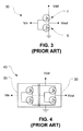
- FIG. 3 illustrates yet another embodiment of a conventional MOSFET inverter 30 including an (upper) p-type enhancement MOSFET 7 and a (lower) n-type enhancement MOSFET 5 .
- the p-type enhancement-mode MOSFET 7 is “complementary” to the n-type MOSFET 5 device in that all voltages and currents are reversed from the n-type device 5 . Consequently, replacing one of the n-MOSFETS in the inverter 20 in FIG. 2 with a p-MOSFET creates a Complementary Metal-Oxide Semiconductor, or “CMOS,” inverter 30 where when one device is on, the other is off, and vice-versa.
- CMOS Complementary Metal-Oxide Semiconductor
- the basic CMOS inverter can be modified to build other complementary circuits as described below.
- the inputs and outputs of two of the CMOS inverters 30 shown in FIG. 3 can be connected in series to create the uni-directional “driver” 40 shown in FIG. 4 .
- the driver 40 is also referred to as a “uni-directional CMOS transmission gate,” or “buffer.” Since there are two inverters in series, Vout in this device will follow Vin. However, due to the inherent “capacitance,” or ability to store energy in the form of opposite charges (e.g., that are segregated in the different layers of material) in each of the transistors, each inverter 30 will require a small period of time before it fully changes the state of its charge.
- the inputs and outputs for several inverters 30 can be “cascaded” to create a delay between the time that Vout changes in response to Vin.
- increasing Vdd relative to ground will reduce this “signal propagation delay,” and vice versa.
- increasing Vdd also increases energy dissipation and reliability concerns due to increased oxide breakdowns, hot-electrons, and other effects that should be avoided.
- Signal propagation delay in cascaded CMOS inverters is further discussed in Rabey, “Digital Integrated Circuits, A Design Perspective,” chapter 5, galley sheets from http://bwrc.eecs.berkeley.edu/Classes/IcBook/NewChapters/ (Prentice Hall, 2d edition 2001) which is incorporated by reference here.
- a signal propagation delay can also be created using a transmission gate, such as the bi-directional full CMOS transmission gate, or “CMOS switch,” 50 shown in FIG. 5 .
- CMOS switch 50 will propagate a delayed voltage signal from Vin to Vout, and in the opposite direction, from Vout to Vin.
- CMOS digital circuits, transmission gates, and propagation delays are also discussed in more detail in Demassa et al., “Digital Integrated Circuits,” pp. 336-476 (John Wiley & Sons 1996) and which is also incorporated herein by reference.
- impedance can be thought of as the effective resistance of a circuit due to its ability to dissipate (through resistance) and store energy (through capacitance and/or inductance) at the same time.
- Impedance matching can then be analogized to an electrical power source having an inherent capacitance (or inductance) that starts to discharge its stored energy at the same time that a “parasitic” capacitance (or inductance) in the connected electrical device, or “load,” starts to recharge. If both of the capacitors (or inductors) have the same electrical properties, i.e. matched impedance, then they will transfer the same amount of “energy” between each other, at roughly the same time, so as to minimize losses during these transfers of “reactive power.”
- the power source for the Motley et al. device includes an operational amplifier, or “op amp.”
- An op amp is basically a “differential amplifier” that responds to a voltage difference between its positive and negative input terminals by producing a larger voltage at its output terminal that is in proportion to the differential input voltage.
- Op amps are generally characterized by their high “gain,” or ability to produce a large output voltage for a relatively small input differential voltage.
- Op amps are also characterized by their high input impedance and low output impedance. Consequently, they can be arranged in amplification circuits, such as the circuit 60 shown in FIG. 6, that draw little input current but can produce as much output current as is necessary in order to maintain an output voltage.
- the output voltage Vout of the amplification circuit 60 is equal to the inverse of the input voltage Vin multiplied by the resistance ratio Rvar/Rin.
- the voltage gain between the input and output of the amplifier circuit 60 can be controlled by varying the resistance Rvar.
- the gain of the amplifier circuit, Vout/Vin is independent of (but less than) the gain “A” of the amplifier itself, the gain of the amplifier circuit is generally unaffected by temperature, input frequency, or device parameters associated with the electronic devices that form the op amp.
- the resulting amplification circuit has a gain of ⁇ 1 so that Vout will equal ⁇ Vin.
- Such amplification circuits are referred to as unity gain buffers, or “voltage followers” since any change in voltage at the output caused by a change in load will cause the op amp to work harder (or less hard) in order to bring the output voltage back up (or down) to match the input voltage.
- the input resistance of the op amp is typically very large relative to the load resistance, the op amp can provide substantial current while drawing nearly zero current from its power source.
- Motley et al. also disclose that PVT compensation can be provided for by voltage follower circuits using the configuration shown in FIG. 7 where Rvar has been replaced with an n-type enhancement MOSFET 5 having its gate terminal connected to the amplifier output, its drain connected to ground, and its source connected to the non-inverting (+) amplifier input. Also, the inverting input to the op amp A is provided with a non-zero reference voltage.
- the MOSFET 5 acts essentially as a variable resister in order to slightly amplify, or attenuate, the voltage follower output Vout in response to PVT effects in the circuit being powered. More specifically, a higher Vout produces a lower resistance through MOSFET 5 so as to lower the feedback voltage, Vfb.
- the gate voltage mirror 80 shown in FIG. 8 .
- the gate voltage mirror 80 includes p-type MOSFET 7 and n-type MOSFET 5 connected in series so that they each have the same source-drain current.
- the gate of the p-type MOSFET is connected to its drain. In this configuration, as Vin on the n-type MOSFET gate (or “Vngate”) goes higher, Vout on the p-type MOSFET gate (or “Vpgate”) will go lower, so as to create a smaller voltage difference between Vngate and Vpgate, and vice versa.
- U.S. Pat. Nos. 5,220,216 and 6,118,310, and European Pat. Application No. 868,026 A1 is also incorporated by reference here.
- U.S. Pat. No. 5,220,216 to Woo discloses CMOS gate having a programmable driving power characteristic for digitally varying its propagation delay.
- U.S. Pat. No. 6,118,310 to Esch discloses a digitally controlled output driver and method for impedance matching.
- EP 868 026 A1 to Watarai et al. discloses a variable delay CMOS circuit for reducing process dependence.
- the present disclosure generally relates to an electronic circuit for processing a signal, and a signal processing method, including variable-delay propagation of a binary signal.
- the circuit may include a transmission gate that receives a binary input signal and propagates a delayed binary output signal corresponding to the input signal.
- the propagation delay is controlled by at least one control signal provided to the transmission gate.
- the control signal may be provided by a voltage mirror in response to a non-binary input signal.
- the non-binary input signal may be set by a variable resistor and the device may include a voltage follower for maintaining the setting of the non-binary input signal.
- the voltage follower may include a gate-controlled feedback loop that compensates for PVT effects.
- the variable-delay transmission gate preferably includes at least two inverters arranged in cascade, and a gate stacked on each side of the inverters. Each of the two stacked gates then controls a current through at least one of the inverters in response to complimentary control signals provided by the voltage mirror.
- each of the attached gates may include at least one, but preferably two, field-effect transistors such as a complementary n- and p-type enhancement-mode MOSFETs.
- FIG. 1 is a circuit diagram for a conventional n-type enhancement-mode MOSFET device
- FIG. 2 is a circuit diagram for a conventional MOSFET inverter
- FIG. 3 is a circuit diagram for a conventional CMOS inverter
- FIG. 4 is a circuit diagram for a conventional uni-directional CMOS transmission gate
- FIG. 5 is a circuit diagram for a conventional, bi-directional CMOS transmission gate
- FIG. 6 is a circuit diagram for a conventional amplification circuit including an op-amp
- FIG. 7 is a circuit diagram for a conventional voltage follower including a transistor-controlled feedback loop
- FIG. 8 is a circuit diagram for a conventional voltage mirror
- FIG. 9 is a circuit diagram for a variable-delay CMOS transmission gate
- FIG. 10 is a circuit diagram for a variable-delay CMOS circuit with PVT control.
- FIG. 11 is a circuit diagram for a variable pulse-width CMOS circuit with PVT control.
- circuits can be implemented in hardware, software, firmware, or a combination thereof.
- the circuit is implemented in hardware that may include any combination of the several technologies, which are all well known in the art, including discrete logic circuits having logic gates for implementing logic functions upon data signals, application specific integrated circuits (ASIC) having appropriate combinational logic gates, programmable gate arrays (PGA), field programmable gate arrays (FPGA), and etc.
- ASIC application specific integrated circuits
- PGA programmable gate arrays
- FPGA field programmable gate arrays
- FIG. 9 is a circuit diagram for a variable-delay transmission gate 90 , and in particular, a variable-delay CMOS transmission gate.
- the variable-delay transmission gate 90 receives a binary input signal and propagates a delayed output signal corresponding to the input signal.
- the variable-delay transmission gate 90 includes a uni-directional CMOS transmission gate 40 having two CMOS inverters 30 arranged in cascade.
- gates 95 and 97 are stacked on each side of each inverter 30 for controlling the source-drain current through the inverters in response to control signals Vpgate and Vngate, respectively.
- Gates 95 and 97 are preferably p-type and n-type enhancement-mode MOSFETs, respectively.
- bipolar transistors including bipolar transistors.
- gates 95 and 97 are configured as inverter control gates 99 .
- FIG. 9 illustrates a uni-directional CMOS transmission gate 40 with two inverters 30 arranged in series (each with its own inverter control gate 99 ), a single inverter control gate 99 , or just one gate 95 , 97 may be provided for controlling the source-drain current through any, or all, of the inverters 30 .
- Other current controlling devices may also be used, such as variable and fixed resistors.
- additional inverters 30 may be added to the uni-directional CMOS transmission gate 40 .
- additional control gates 99 may be added to the variable-delay transmission gate 90 .
- FIG. 10 is a circuit diagram for a variable-delay CMOS circuit 100 with PVT control.
- the variable-delay CMOS transmission gate 90 is preferably controlled by complementary control signals, Vpgate and Vngate, which are preferably provided by a voltage mirror 80 for controlling the propagation delay through the transmission gate 90 .
- Vpgate and Vngate may also be provided by other complementary voltage sources besides voltage mirrors.
- the voltage mirror 80 is preferably driven by a voltage follower 70 , or other voltage source, having its input voltage determined by the setting of the external variable resistor Rext.
- the voltage follower 70 is provided with a feedback loop that is controlled by gate 75 so as to compensate for PVT effects in the remainder of the variable-delay CMOS circuit 100 .
- the external resistor Rext is preferably arranged remote from the remainder of the circuit 100 so as to allow for convenient, manual adjustment.
- Rext may be a local and/or non-variable resistor that is chosen for a certain propagation delay.
- Rext may also be supplemented and/or replaced by a voltage-controlled gate.
- CMOS inverter 30 During operation, a binary input signal “IN” is applied to CMOS inverter 30 and output to variable-delay CMOS transmission gate 90 .
- the propagation delay for the inverted signal is then controlled by the signals Vpgate and Vngate, which are set by the voltage mirror 80 in response to the output of the current follower 70 .
- the propagation delay of the signal through the variable-delay CMOS transmission gate 90 can be controlled by varying the resistance of Rext without changing Vdd.
- an additional fixed propagation delay can be added to the output from the variable-delay gate 90 by, for example, further processing the signal through the bidirectional CMOS transmission gate 50 .
- a unidirectional CMOS transmission gate 40 or another variable-delay CMOS transmission gate 90 may be used.
- the delayed signal output from the variable-delay transmission gate 90 may then be compared to the further delayed output from the transmission gate 50 to create a clock pulse “OUT.”
- an XOR logic gate 150 may be provided for producing the clock pulse “OUT” based upon the delayed signal in line 155 and the further delayed signal in line 157 .
- the CMOS transmission gate 50 may also be located ahead of the variable-delay transmission gate 90 .
- FIG. 11 is a circuit diagram for a variable pulse-width CMOS circuit 110 with PVT control.
- the variable pulse-width circuit 110 is substantially the same as the variable-delay circuit 100 in FIG. 10 except that the bi-directional transmission gate 50 has been removed and line 157 has been connected to the binary input signal IN. Output signal OUT 2 will therefore have a different pulse-width than input signal IN, where the pulse-width is controlled by the resistance of the external resister Rext.
Abstract
Description
Claims (23)
Priority Applications (1)
| Application Number | Priority Date | Filing Date | Title |
|---|---|---|---|
| US09/796,306 US6522185B2 (en) | 2001-02-28 | 2001-02-28 | Variable delay CMOS circuit with PVT control |
Applications Claiming Priority (1)
| Application Number | Priority Date | Filing Date | Title |
|---|---|---|---|
| US09/796,306 US6522185B2 (en) | 2001-02-28 | 2001-02-28 | Variable delay CMOS circuit with PVT control |
Publications (2)
| Publication Number | Publication Date |
|---|---|
| US20020118056A1 US20020118056A1 (en) | 2002-08-29 |
| US6522185B2 true US6522185B2 (en) | 2003-02-18 |
Family
ID=25167879
Family Applications (1)
| Application Number | Title | Priority Date | Filing Date |
|---|---|---|---|
| US09/796,306 Expired - Lifetime US6522185B2 (en) | 2001-02-28 | 2001-02-28 | Variable delay CMOS circuit with PVT control |
Country Status (1)
| Country | Link |
|---|---|
| US (1) | US6522185B2 (en) |
Cited By (10)
| Publication number | Priority date | Publication date | Assignee | Title |
|---|---|---|---|---|
| US20040246045A1 (en) * | 2001-05-17 | 2004-12-09 | Kyu-Nam Lim | Voltage and time control circuits and methods of operating the same |
| US20050242831A1 (en) * | 2004-04-30 | 2005-11-03 | Linam David L | Tristateable cmos driver with controlled slew rate for integrated circuit i/o pads |
| US20050242830A1 (en) * | 2004-04-30 | 2005-11-03 | Humphrey Guy H | Hybrid binary/thermometer code for controlled-voltage integrated circuit output drivers |
| US20060097759A1 (en) * | 2004-11-08 | 2006-05-11 | Tetsuro Omori | Current driver |
| US20070024317A1 (en) * | 2005-07-29 | 2007-02-01 | Hansen James E | Apparatus for obtaining precision integrated resistors |
| US20080143376A1 (en) * | 2004-06-08 | 2008-06-19 | Transmeta Corporation | Leakage efficient anti-glitch filter |
| US20080252364A1 (en) * | 2007-04-12 | 2008-10-16 | Kuo-Yu Chou | Reference Voltage Generator for Analog-To-Digital Converter Circuit |
| US20110204958A1 (en) * | 2008-05-08 | 2011-08-25 | Kpit Cummins Infosystems Ltd., | Method and system for open loop compensation of delay variations in a delay line |
| US8294503B1 (en) * | 2004-11-22 | 2012-10-23 | Marvell International Ltd. | Method and apparatus for reducing jitter in a transmitter |
| US20240085939A1 (en) * | 2022-09-14 | 2024-03-14 | SK Hynix Inc. | Clock generating circuit and clock distribution network and semiconductor apparatus including the clock generating circuit |
Families Citing this family (1)
| Publication number | Priority date | Publication date | Assignee | Title |
|---|---|---|---|---|
| US8531241B1 (en) | 2011-01-26 | 2013-09-10 | Applied Micro Circuits Corporation | System and method for process, voltage, temperature (PVT) stable differential amplifier transfer function |
Citations (14)
| Publication number | Priority date | Publication date | Assignee | Title |
|---|---|---|---|---|
| US5039893A (en) * | 1984-07-31 | 1991-08-13 | Yamaha Corporation | Signal delay device |
| US5192886A (en) * | 1990-03-15 | 1993-03-09 | Hewlett-Packard Company | Sub-nanosecond calibrated delay line structure |
| US5220216A (en) | 1992-01-02 | 1993-06-15 | Woo Ann K | Programmable driving power of a CMOS gate |
| US5581197A (en) * | 1995-05-31 | 1996-12-03 | Hewlett-Packard Co. | Method of programming a desired source resistance for a driver stage |
| US5712583A (en) * | 1995-11-13 | 1998-01-27 | International Business Machines Corporation | Clock phase alignment using frequency comparison |
| US5731727A (en) * | 1994-11-01 | 1998-03-24 | Mitsubishi Denki Kabushiki Kaisha | Voltage control type delay circuit and internal clock generation circuit using the same |
| EP0868026A1 (en) | 1996-01-22 | 1998-09-30 | Nec Corporation | Variable delay circuit |
| US5886946A (en) | 1996-04-26 | 1999-03-23 | Mitsubishi Denki Kabushiki Kaisha | Semiconductor memory device allowing reduction in power consumption during standby |
| US5936986A (en) * | 1996-07-30 | 1999-08-10 | Bayer Corporation | Methods and apparatus for driving a laser diode |
| US5998983A (en) * | 1997-12-10 | 1999-12-07 | Mhs | Device for generating a DC reference voltage |
| US6118310A (en) | 1998-11-04 | 2000-09-12 | Agilent Technologies | Digitally controlled output driver and method for impedance matching |
| US6175605B1 (en) * | 1998-03-25 | 2001-01-16 | Vanguard International Semiconductor Corporation | Edge triggered delay line, a multiple adjustable delay line circuit, and an application of same |
| US6178123B1 (en) * | 1998-04-27 | 2001-01-23 | Mitsubishi Denki Kabushiki Kaisha | Semiconductor device with circuit for phasing internal clock signal |
| US6262609B1 (en) * | 1998-09-11 | 2001-07-17 | Research In Motion Limited | Closed-loop voltage-to-frequency converter |
-
2001
- 2001-02-28 US US09/796,306 patent/US6522185B2/en not_active Expired - Lifetime
Patent Citations (15)
| Publication number | Priority date | Publication date | Assignee | Title |
|---|---|---|---|---|
| US5039893A (en) * | 1984-07-31 | 1991-08-13 | Yamaha Corporation | Signal delay device |
| US5192886A (en) * | 1990-03-15 | 1993-03-09 | Hewlett-Packard Company | Sub-nanosecond calibrated delay line structure |
| US5420531A (en) * | 1990-03-15 | 1995-05-30 | Hewlett-Packard Company | Sub-nanosecond calibrated delay line structure |
| US5220216A (en) | 1992-01-02 | 1993-06-15 | Woo Ann K | Programmable driving power of a CMOS gate |
| US5731727A (en) * | 1994-11-01 | 1998-03-24 | Mitsubishi Denki Kabushiki Kaisha | Voltage control type delay circuit and internal clock generation circuit using the same |
| US5581197A (en) * | 1995-05-31 | 1996-12-03 | Hewlett-Packard Co. | Method of programming a desired source resistance for a driver stage |
| US5712583A (en) * | 1995-11-13 | 1998-01-27 | International Business Machines Corporation | Clock phase alignment using frequency comparison |
| EP0868026A1 (en) | 1996-01-22 | 1998-09-30 | Nec Corporation | Variable delay circuit |
| US5886946A (en) | 1996-04-26 | 1999-03-23 | Mitsubishi Denki Kabushiki Kaisha | Semiconductor memory device allowing reduction in power consumption during standby |
| US5936986A (en) * | 1996-07-30 | 1999-08-10 | Bayer Corporation | Methods and apparatus for driving a laser diode |
| US5998983A (en) * | 1997-12-10 | 1999-12-07 | Mhs | Device for generating a DC reference voltage |
| US6175605B1 (en) * | 1998-03-25 | 2001-01-16 | Vanguard International Semiconductor Corporation | Edge triggered delay line, a multiple adjustable delay line circuit, and an application of same |
| US6178123B1 (en) * | 1998-04-27 | 2001-01-23 | Mitsubishi Denki Kabushiki Kaisha | Semiconductor device with circuit for phasing internal clock signal |
| US6262609B1 (en) * | 1998-09-11 | 2001-07-17 | Research In Motion Limited | Closed-loop voltage-to-frequency converter |
| US6118310A (en) | 1998-11-04 | 2000-09-12 | Agilent Technologies | Digitally controlled output driver and method for impedance matching |
Cited By (19)
| Publication number | Priority date | Publication date | Assignee | Title |
|---|---|---|---|---|
| US20040246045A1 (en) * | 2001-05-17 | 2004-12-09 | Kyu-Nam Lim | Voltage and time control circuits and methods of operating the same |
| US20050242831A1 (en) * | 2004-04-30 | 2005-11-03 | Linam David L | Tristateable cmos driver with controlled slew rate for integrated circuit i/o pads |
| US20050242830A1 (en) * | 2004-04-30 | 2005-11-03 | Humphrey Guy H | Hybrid binary/thermometer code for controlled-voltage integrated circuit output drivers |
| US7005886B2 (en) | 2004-04-30 | 2006-02-28 | Agilent Technologies, Inc. | Tristateable CMOS driver with controlled slew rate for integrated circuit I/O pads |
| US7088129B2 (en) | 2004-04-30 | 2006-08-08 | Avago Technologies General Ip (Singapore) Pte. Ltd. | Hybrid binary/thermometer code for controlled-voltage integrated circuit output drivers |
| US20060290541A1 (en) * | 2004-04-30 | 2006-12-28 | Humphrey Guy H | Hybrid binary/thermometer code for controlled-voltage integrated circuit output drivers |
| US7400272B2 (en) | 2004-04-30 | 2008-07-15 | Avago Technologies General Ip Pte Ltd | Hybrid binary/thermometer code for controlled-voltage integrated circuit output drivers |
| US20080143376A1 (en) * | 2004-06-08 | 2008-06-19 | Transmeta Corporation | Leakage efficient anti-glitch filter |
| US7724025B2 (en) * | 2004-06-08 | 2010-05-25 | Robert Masleid | Leakage efficient anti-glitch filter |
| US20060097759A1 (en) * | 2004-11-08 | 2006-05-11 | Tetsuro Omori | Current driver |
| US7327170B2 (en) * | 2004-11-08 | 2008-02-05 | Matsushita Electric Industrial Co., Ltd. | Current driver |
| US8294503B1 (en) * | 2004-11-22 | 2012-10-23 | Marvell International Ltd. | Method and apparatus for reducing jitter in a transmitter |
| US8698537B1 (en) | 2004-11-22 | 2014-04-15 | Marvell International Ltd. | Method and apparatus for reducing jitter in a transmitter |
| US20070024317A1 (en) * | 2005-07-29 | 2007-02-01 | Hansen James E | Apparatus for obtaining precision integrated resistors |
| US20080252364A1 (en) * | 2007-04-12 | 2008-10-16 | Kuo-Yu Chou | Reference Voltage Generator for Analog-To-Digital Converter Circuit |
| US7777559B2 (en) * | 2007-04-12 | 2010-08-17 | Novatek Microelectronics Corp. | Reference voltage generator for analog-to-digital converter circuit |
| US20110204958A1 (en) * | 2008-05-08 | 2011-08-25 | Kpit Cummins Infosystems Ltd., | Method and system for open loop compensation of delay variations in a delay line |
| US8390356B2 (en) * | 2008-05-08 | 2013-03-05 | Kpit Cummins Infosystems, Ltd. | Method and system for open loop compensation of delay variations in a delay line |
| US20240085939A1 (en) * | 2022-09-14 | 2024-03-14 | SK Hynix Inc. | Clock generating circuit and clock distribution network and semiconductor apparatus including the clock generating circuit |
Also Published As
| Publication number | Publication date |
|---|---|
| US20020118056A1 (en) | 2002-08-29 |
Similar Documents
| Publication | Publication Date | Title |
|---|---|---|
| US10797694B2 (en) | Switch circuit and method of switching radio frequency signals | |
| US11196414B2 (en) | Circuit and method for controlling charge injection in radio frequency switches | |
| CN110771043B (en) | Timing controller for dead time control | |
| JP2991904B2 (en) | Integrated circuit for signal processing | |
| US7613442B1 (en) | Switch circuit and method of switching radio frequency signals | |
| US6522185B2 (en) | Variable delay CMOS circuit with PVT control | |
| JPH05267603A (en) | Integrated circuit | |
| US20090167368A1 (en) | Pre-driver circuit having a post-boost circuit | |
| CN114731140A (en) | On-time acceleration of cascaded amplifiers | |
| CN113810034A (en) | RF switch stack with charge control element | |
| US7183816B2 (en) | Circuit and method for switching an electrical load on after a delay | |
| US6781434B2 (en) | Low charge-dump transistor switch | |
| US20030042970A1 (en) | Controllable reference voltage circuit with power supply isolation | |
| EP0435600A2 (en) | Integrated sample and hold circuits | |
| JP2002135066A (en) | Source follower circuit | |
| US11855642B1 (en) | Programmable delay circuit including threshold-voltage programmable field effect transistor | |
| JPH06216727A (en) | Delay time variable logic circuit | |
| JPH10322193A (en) | Logical gate circuit |
Legal Events
| Date | Code | Title | Description |
|---|---|---|---|
| AS | Assignment |
Owner name: AGILENT TECHNOLOGIES, INC., CALIFORNIA Free format text: ASSIGNMENT OF ASSIGNORS INTEREST;ASSIGNORS:HELT, CHRISTOPHER GEORGE;HUMPHREY, GUY H.;REEL/FRAME:011697/0844 Effective date: 20010329 |
|
| STCF | Information on status: patent grant |
Free format text: PATENTED CASE |
|
| AS | Assignment |
Owner name: AVAGO TECHNOLOGIES GENERAL IP PTE. LTD., SINGAPORE Free format text: ASSIGNMENT OF ASSIGNORS INTEREST;ASSIGNOR:AGILENT TECHNOLOGIES, INC.;REEL/FRAME:017207/0020 Effective date: 20051201 |
|
| FPAY | Fee payment |
Year of fee payment: 4 |
|
| FPAY | Fee payment |
Year of fee payment: 8 |
|
| AS | Assignment |
Owner name: DEUTSCHE BANK AG NEW YORK BRANCH, AS COLLATERAL AGENT, NEW YORK Free format text: PATENT SECURITY AGREEMENT;ASSIGNOR:AVAGO TECHNOLOGIES GENERAL IP (SINGAPORE) PTE. LTD.;REEL/FRAME:032851/0001 Effective date: 20140506 Owner name: DEUTSCHE BANK AG NEW YORK BRANCH, AS COLLATERAL AG Free format text: PATENT SECURITY AGREEMENT;ASSIGNOR:AVAGO TECHNOLOGIES GENERAL IP (SINGAPORE) PTE. LTD.;REEL/FRAME:032851/0001 Effective date: 20140506 |
|
| FPAY | Fee payment |
Year of fee payment: 12 |
|
| AS | Assignment |
Owner name: AVAGO TECHNOLOGIES GENERAL IP (SINGAPORE) PTE. LTD., SINGAPORE Free format text: TERMINATION AND RELEASE OF SECURITY INTEREST IN PATENT RIGHTS (RELEASES RF 032851-0001);ASSIGNOR:DEUTSCHE BANK AG NEW YORK BRANCH, AS COLLATERAL AGENT;REEL/FRAME:037689/0001 Effective date: 20160201 Owner name: AVAGO TECHNOLOGIES GENERAL IP (SINGAPORE) PTE. LTD Free format text: TERMINATION AND RELEASE OF SECURITY INTEREST IN PATENT RIGHTS (RELEASES RF 032851-0001);ASSIGNOR:DEUTSCHE BANK AG NEW YORK BRANCH, AS COLLATERAL AGENT;REEL/FRAME:037689/0001 Effective date: 20160201 |
|
| AS | Assignment |
Owner name: BANK OF AMERICA, N.A., AS COLLATERAL AGENT, NORTH CAROLINA Free format text: PATENT SECURITY AGREEMENT;ASSIGNOR:AVAGO TECHNOLOGIES GENERAL IP (SINGAPORE) PTE. LTD.;REEL/FRAME:037808/0001 Effective date: 20160201 Owner name: BANK OF AMERICA, N.A., AS COLLATERAL AGENT, NORTH Free format text: PATENT SECURITY AGREEMENT;ASSIGNOR:AVAGO TECHNOLOGIES GENERAL IP (SINGAPORE) PTE. LTD.;REEL/FRAME:037808/0001 Effective date: 20160201 |
|
| AS | Assignment |
Owner name: AVAGO TECHNOLOGIES GENERAL IP (SINGAPORE) PTE. LTD Free format text: CORRECTIVE ASSIGNMENT TO CORRECT THE NAME OF THE ASSIGNEE PREVIOUSLY RECORDED ON REEL 017207 FRAME 0020. ASSIGNOR(S) HEREBY CONFIRMS THE ASSIGNMENT;ASSIGNOR:AGILENT TECHNOLOGIES, INC.;REEL/FRAME:038633/0001 Effective date: 20051201 |
|
| AS | Assignment |
Owner name: AVAGO TECHNOLOGIES GENERAL IP (SINGAPORE) PTE. LTD., SINGAPORE Free format text: TERMINATION AND RELEASE OF SECURITY INTEREST IN PATENTS;ASSIGNOR:BANK OF AMERICA, N.A., AS COLLATERAL AGENT;REEL/FRAME:041710/0001 Effective date: 20170119 Owner name: AVAGO TECHNOLOGIES GENERAL IP (SINGAPORE) PTE. LTD Free format text: TERMINATION AND RELEASE OF SECURITY INTEREST IN PATENTS;ASSIGNOR:BANK OF AMERICA, N.A., AS COLLATERAL AGENT;REEL/FRAME:041710/0001 Effective date: 20170119 |
|
| AS | Assignment |
Owner name: AVAGO TECHNOLOGIES INTERNATIONAL SALES PTE. LIMITE Free format text: MERGER;ASSIGNOR:AVAGO TECHNOLOGIES GENERAL IP (SINGAPORE) PTE. LTD.;REEL/FRAME:047195/0026 Effective date: 20180509 |
|
| AS | Assignment |
Owner name: AVAGO TECHNOLOGIES INTERNATIONAL SALES PTE. LIMITE Free format text: CORRECTIVE ASSIGNMENT TO CORRECT THE EFFECTIVE DATE OF MERGER PREVIOUSLY RECORDED ON REEL 047195 FRAME 0026. ASSIGNOR(S) HEREBY CONFIRMS THE MERGER;ASSIGNOR:AVAGO TECHNOLOGIES GENERAL IP (SINGAPORE) PTE. LTD.;REEL/FRAME:047477/0423 Effective date: 20180905 |
|
| AS | Assignment |
Owner name: BROADCOM INTERNATIONAL PTE. LTD., SINGAPORE Free format text: ASSIGNMENT OF ASSIGNORS INTEREST;ASSIGNOR:AVAGO TECHNOLOGIES INTERNATIONAL SALES PTE. LIMITED;REEL/FRAME:053771/0901 Effective date: 20200826 |